Article

Three-Level Unidirectional Rectifiers under Non-Unity Power Factor Operation and Unbalanced Split DC-Link Loading: Analytical and Experimental Assessment

Energy Department “Galileo Ferraris”, Politecnico di Torino, 10129 Torino, Italy
*
Author to whom correspondence should be addressed.
Energies 2021, 14(17), 5280; https://doi.org/10.3390/en14175280
Submission received: 21 June 2021 / Revised: 16 August 2021 / Accepted: 23 August 2021 / Published: 25 August 2021
(This article belongs to the Special Issue Control and Topologies of Grid Connected Converters)

Abstract

:
Three-phase three-level unidirectional rectifiers are among the most adopted topologies for general active rectification, achieving an excellent compromise between cost, complexity and overall performance. The unidirectional nature of these rectifiers negatively affects their operation, e.g., distorting the input currents around the zero-crossings, limiting the maximum converter-side displacement power factor, reducing the split DC-link mid-point current capability and limiting the converter ability to compensate the low-frequency DC-link mid-point voltage oscillation. In particular, the rectifier operation under non-unity power factor and/or under constant zero-sequence voltage injection (i.e., when unbalanced split DC-link loading occurs) typically yields large and uncontrolled input current distortion, effectively limiting the acceptable operating region of the converter. Although high bandwidth current control loops and enhanced phase current sampling strategies may improve the rectifier input current distortion, especially at light load, these approaches lose effectiveness when significant phase-shift between voltage and current is required and/or a constant zero-sequence voltage must be injected. Therefore, this paper proposes a complete analysis and performance assessment of three-level unidirectional rectifiers under non-unity power factor operation and unbalanced split DC-link loading. First, the theoretical operating limits of the converter in terms of zero-sequence voltage, modulation index, power factor angle, maximum DC-link mid-point current and minimum DC-link mid-point charge ripple are derived. Leveraging the derived zero-sequence voltage limits, a unified carrier-based pulse-width modulation (PWM) approach enabling the undistorted operation of the rectifier in all feasible operating conditions is thus proposed. Moreover, novel analytical expressions defining the maximum rectifier mid-point current capability and the minimum peak-to-peak DC-link mid-point charge ripple as functions of both modulation index and power factor angle are derived, the latter enabling a straightforward sizing of the split DC-link capacitors. The theoretical analysis is verified on a 30 k W , 20 k Hz T-type rectifier prototype, designed for electric vehicle ultra-fast battery charging. The input phase current distortion, the maximum mid-point current capability and the minimum mid-point charge ripple are experimentally assessed across all rectifier operating points, showing excellent performance and accurate agreement with the analytical predictions.

1. Introduction

Pulse-width modulated (PWM) active rectification is a fundamental requirement for the supply of modern high-power electrical systems, as it ensures lower distortion, higher performance and wider regulation capability with respect to passive and/or hybrid rectification solutions [1,
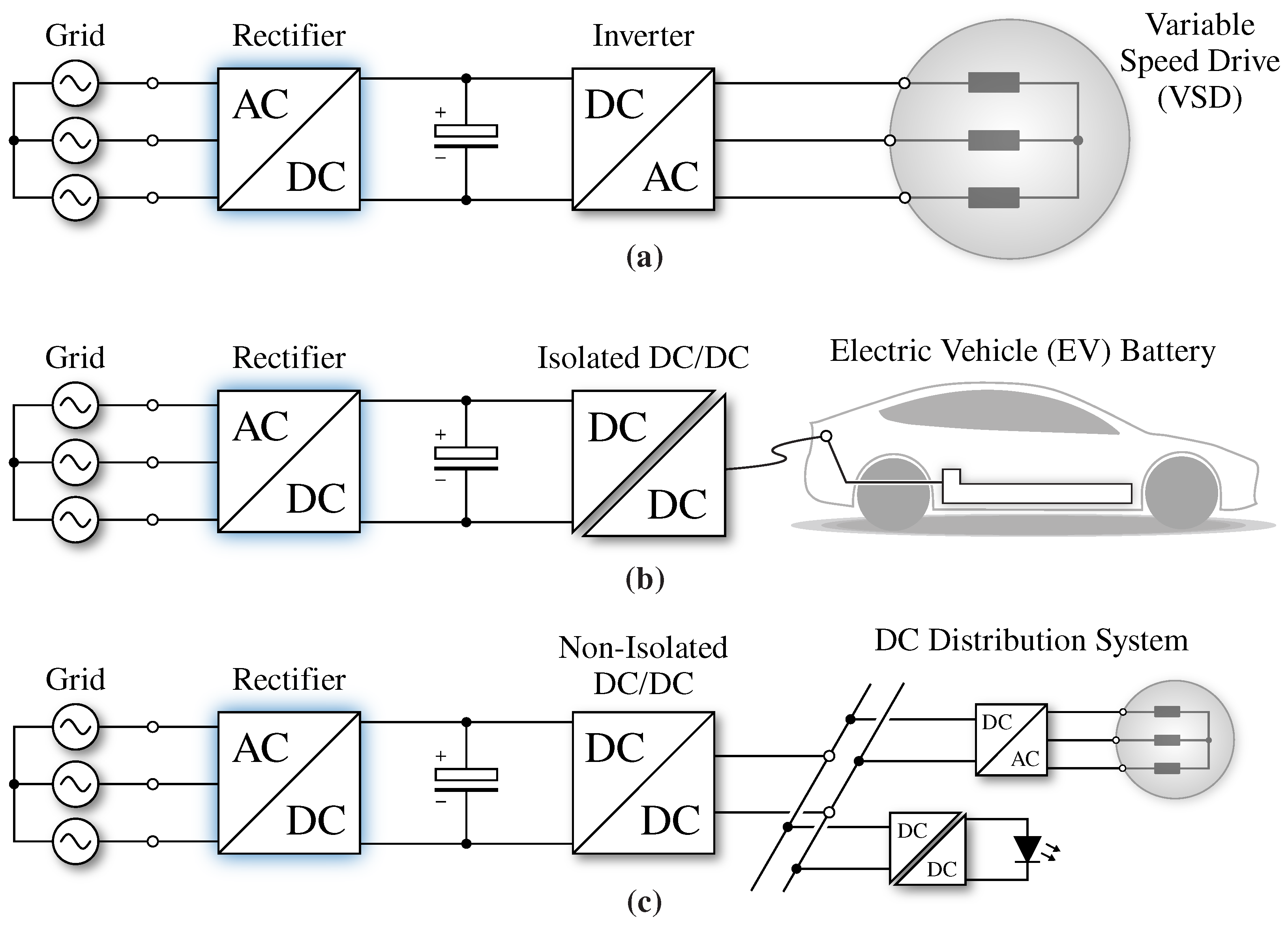
2]. Typically, the supply of high-power loads from the three-phase grid is performed in two stages, as illustrated in Figure 1, the first being the rectifier or active front-end (AFE). The second conversion stage depends on the electrical system being supplied, such as three-phase DC/AC inverters for variable-speed drives (VSDs) or uninterruptible power supplies (UPSs) (Figure 1a), isolated DC/DC converters for electric vehicle DC fast charging, telecommunication and data center power supplies, lighting systems or induction heating (Figure 1b), and non-isolated DC/DC converters for DC distribution systems, high-power DC loads or DC microgrids (Figure 1c).
General active rectification is typically performed by means of a conventional two-level inverter, due to its simplicity, robustness and intrinsic bidirectional capabilities. However, this topology has two major drawbacks, as it features a two-level output voltage waveform and requires semiconductor devices with relatively high voltage rating, both negatively affecting the converter losses and the grid-side filter size. Even though modern semiconductor technologies (e.g., high-voltage SiC MOSFETs) can substantially improve the two-level inverter performance by reducing losses and allowing for higher operating frequencies, multi-level converter solutions have demonstrated higher achievable performance, both in terms of efficiency and power density [3,4,5]. In fact, these topologies simultaneously reduce the stress on the AC-side filter components and allow the employment of semiconductor devices with lower voltage rating and thus better figures of merit [6].
When the power is only required to flow from the grid to the load, three-level unidirectional rectifiers represent perfect candidates for general active rectification [7,8,9]. In particular, these converter topologies trade higher efficiency and power density for a slight complexity increase, thus achieving improved performance with respect to conventional two-level inverters [3,4,5].
Besides high efficiency and high power density, the key requirements of a three-level rectifier can be summarized in (1) sinusoidal input current shaping, featuring low distortion and harmonics; (2) DC-link voltage regulation according to the desired reference value; and (3) control of the DC-link mid-point voltage deviation under normal operating conditions (i.e., balanced split DC-link loading). Other desired features include, but are not limited to, (4) minimization of the DC-link mid-point third-harmonic voltage oscillation [8,10], which directly affects the size of the DC-link capacitors and may be hard to reject by the subsequent conversion stage [11]; (5) full control of the DC-link mid-point voltage deviation under unbalanced split DC-link loading [7], which may occur when separate DC/DC units are connected to the two DC-link halves (e.g., in DC fast chargers [12]); and (6) operation under non-unity power factor, to support the reactive energy flows in distribution grids [13]. All the aforementioned required and desired features can be addressed either with a proper converter control strategy (1)–(6) [14,15,16], with an accurate AC-side filter design (1) [17,18], or with an appropriate selection of the converter modulation strategy (4) [8,19]. In particular, (6) has not been explored in the literature and is increasingly becoming a desired feature of modern rectifiers, as distribution system operators (DSOs) are starting to charge end consumers for the injection/withdrawal of reactive energy into/from the grid [20]. If properly controlled, existing unidirectional rectifiers could in fact actively compensate this reactive power excess and/or substitute traditional power factor correction capacitor banks, benefiting the DSO and improving the system power quality.
The main challenges in achieving (1)–(6) are strictly related to the unidirectional nature of three-level rectifiers. One major issue is the discontinuous conduction mode (DCM) operation of the converter around the current zero-crossings, which, if not correctly addressed, can lead to unacceptable phase current distortion in light load conditions [21]. Moreover, unidirectional rectifiers are characterized by narrower operating limits with respect to their two-level and three-level bidirectional counterparts, mainly affecting the operation under non-unity power factor, the maximum DC-link mid-point current capability and the converter ability to compensate the low-frequency DC-link mid-point voltage oscillation. In particular, the rectifier operation under non-unity power factor and/or under constant zero-sequence voltage injection (i.e., when unbalanced split DC-link loading occurs) typically yields large and uncontrolled input current distortion, as reported in several previous works [22,23,24,25,26,27], practically limiting the acceptable operating region of the converter. Although high current control loop bandwidth and enhanced phase current sampling strategies may improve the rectifier input current distortion [16], especially in light load conditions, these approaches lose effectiveness when significant voltage-to-current phase-shift and/or zero-sequence voltage injection are required.
Mainly because of the aforementioned reason, several papers dealing with the analysis and the control of three-level unidirectional rectifiers under diverse operating conditions have been published in the literature [7,8,9,14,15,22,23,24,25,26,27,28,29].
In particular, [7,8,9] are the first papers analyzing the operational limits and the DC-link mid-point current capability of unidirectional three-level rectifiers, identifying a direct relation between the allocation of the converter redundant switching states (i.e., strictly related to the zero-sequence voltage injection) and the mid-point current generation process. Moreover, a preliminary attempt to control the DC-link mid-point voltage deviation is proposed in [9], acting on the zero-sequence current reference of a hysteresis current controller. However, no details on the operation of the rectifier with non-unity power factor are provided.
A detailed small-signal analysis of unidirectional three-level rectifiers is described in [14] and a complete multi-loop control strategy is proposed, enabling the accurate regulation of the DC-link mid-point voltage deviation. The same authors develop in [28] a carrier-based modulation strategy for three-level rectifiers based on the translation of conventional space vector dwell times into an equivalent zero-sequence duty-cycle injection. With this approach, the zero-sequence voltage limits of the converter are correctly taken into account, resulting in undistorted input currents under non-unity power factor operation and when a constant zero-sequence voltage is injected (i.e., to regulate the mid-point current). Nevertheless, the proposed implementation is quite complex, and no current distortion assessment is performed.
A direct carrier-based approach for undistorted operation under non-unity power factor is first proposed in [22]. This method is based on the addition of a zero-sequence voltage component to all bridge-leg voltage references, to make sure that the sign of the reference voltages is always equal to their respective phase currents. In fact, the unidirectional nature of the rectifier does not allow for the generation of a bridge-leg voltage with different sign as the current flowing in it. This approach, however, only solves the distortion issue for non-unity power factor operation (i.e., it has no general validity) and does not ensure sinusoidal operation when a constant zero-sequence voltage is injected.
In a similar way, [23,24,25,26,27,29] try to address the input phase current distortion deriving from non-unity power factor operation either by injecting a suitable zero-sequence voltage component for carrier-based approaches, or by correctly allocating the redundant switching states in space vector-based implementations. Nevertheless, none of these papers proposes a general and/or unified approach to ensure undistorted operation also under constant zero-sequence voltage injection.
Finally, a general methodology ensuring that the sign of the rectifier bridge-leg voltages remains equal to their respective phase currents in every operating condition is identified in [15]. This approach is based on the saturation of the reference zero-sequence voltage according to straightforward analytical relations and is theoretically able to ensure undistorted input current for both non-unity power factor operation and constant zero-sequence voltage injection. However, the converter distortion performances are not assessed and the effects of the zero-sequence voltage saturation on the DC-link mid-point current are not investigated.
As a further note, several considerations and analysis methods that have been specifically developed for three-level bidirectional inverters (e.g., to estimate and/or minimize the DC-link mid-point current and voltage oscillation [10,30,31,32,33,34], to control the DC-link mid-point voltage deviation with/without load unbalance [33,34], etc.) or the addition of an independent neutral module in four wire systems (i.e., to independently control the DC-link mid-point current in every operating condition [35,36]) have general validity and could thus be as well applied to three-level unidirectional rectifiers with minor modifications. Nevertheless, no additional and/or relevant elements with respect to the presented literature survey on unidirectional topologies has been identified.
Even though the operation and the control of three-level rectifiers have been thoroughly analyzed in the literature, according to the authors’ best knowledge, a clear and complete analysis of the effects of non-unity power factor operation and constant zero-sequence voltage injection (i.e., operation under unbalanced split DC-link loading), has yet to be provided. In particular, no simple and unified carrier-based PWM approach ensuring undistorted operation of unidirectional rectifiers across their entire operating region has been proposed and verified experimentally. Moreover, no analytical expressions for the converter maximum DC-link mid-point current capability and minimum DC-link mid-point charge ripple for variable modulation index and power factor angle have been identified, forcing converter designers to make use of numerical and/or circuit simulations.
Therefore, this paper proposes a complete analysis of three-level unidirectional rectifiers under non-unity power factor operation and zero-sequence voltage injection, with the main goal of providing a simple and comprehensive overview of the rectifier limits and performance. The major contributions of this work are: (1) the adoption of a unified carrier-based PWM approach ensuring undistorted operation of the rectifier in every feasible operating condition (i.e., for variable power factor and variable zero-sequence voltage injection), based on the saturation of the zero-sequence voltage reference; (2) the analytical derivation of the DC-link mid-point current limits over the complete operating range of the rectifier; and (3) the analytical derivation of the minimum low-frequency (i.e., third-harmonic) mid-point peak-to-peak charge ripple for all feasible modulation index and power factor angle values. In particular, (3) allows the sizing of the split DC-link capacitors of three-level rectifiers with a straightforward analytical formula.
This paper is structured as follows. In Section 2 the operational basics of three-level unidirectional rectifiers are described and the converter limits in terms of zero-sequence voltage, modulation index, power factor angle, maximum DC-link mid-point current and minimum mid-point charge ripple are derived, leveraging the analytical approaches reported in Appendices Appendix A and Appendix B. In Section 3 the proposed analysis is verified experimentally on a digitally controlled 30 k W T-type converter prototype, assessing the input phase current distortion, the maximum mid-point current capability and the minimum mid-point charge ripple across all rectifier operating points. Finally, Section 4 summarizes and concludes this work.

2. Converter Operation and Limits

The structure of a three-level rectifier is schematically represented in Figure 2. The three-phase AC inputs are passively connected to the upper and lower DC-link rails through diodes (i.e., unidirectionally), while three bipolar/bidirectional 4-quadrant (4Q) switches actively connect them to the DC-link mid-point. In practice, the 4Q switch may be realized in different ways that are highlighted in Figure 2a–c [37], where switch implementations (b) and (c) may be also integrated within the diode bridge, thus requiring diodes with lower blocking voltage capability [1].
To simplify the following analysis, the DC-side loads connected to the upper and lower DC-link halves are assumed as ideal current-sources, while no inner grid impedance and no AC-side filter are considered. It is worth noting that these simplifying assumptions do not affect the general validity of the following analysis.

2.1. Basics of Operation

The system state variables defining the converter operation are the boost inductor currents i a , i b , i c and the DC-link capacitor voltages V pm , V mn (see Figure 2). Due to the three-phase three-wire nature of the system (i.e., i a + i b + i c = 0 ), the total number of state variables is reduced to four [16]. Moreover, the DC-link capacitor voltages V pm and V mn can be rearranged to define the DC-link voltage V dc and the mid-point voltage deviation V m , respectively
V dc = V pm + V mn ,
V m = V pm V mn .
It is worth noting that in normal operating conditions V m = 0 , assuming balanced split DC-link voltages V pm = V mn = V dc / 2 .
Disregarding the voltage drop at fundamental frequency across the boost inductance L (i.e., negligible for converters with high pulse ratios [8]), the phase voltage local averages applied by the rectifier can be expressed as
v a u a = M V dc 2 cos ( ϑ ) v b u b = M V dc 2 cos ( ϑ 2 3 π ) v c u c = M V dc 2 cos ( ϑ 4 3 π ) ,
where ϑ = ω t = 2 π f t is the phase angle, f is the grid frequency, M = 2 V / V dc is the modulation index of the rectifier and V is the phase voltage peak value. For the sake of completeness, the phase voltages v a , v b , v c can be represented with a space vector approach as
V = 2 3 v a e j 0 + v b e j 2 π / 3 + v c e j 4 π / 3 ,
where j is the imaginary unit.
Neglecting the switching ripple, the controlled phase currents are sinusoidal and are therefore expressed by
i a = I cos ( ϑ φ ) i b = I cos ( ϑ 2 3 π φ ) i c = I cos ( ϑ 4 3 π φ ) ,
where I is the phase current peak value and φ is the converter-side power factor angle (i.e., φ = v x i x with x = a , b , c ). As with the phase voltages, i a , i b , i c can be expressed with an equivalent space vector representation as
I = 2 3 i a e j 0 + i b e j 2 π / 3 + i c e j 4 π / 3 .
Due to the structure of a three-level unidirectional rectifier, the AC terminal of each bridge-leg may be actively connected to the DC-link mid-point (switch in the ON state) or, depending on the phase current direction, passively connected to either the positive or negative DC-link rails (switch in the OFF state). Consequently, the voltage applied by each bridge-leg with respect to the DC-link mid-point can assume three different values (i.e., 0, + V dc / 2 , V dc / 2 ), which correspond to three separate switching states. Overall, the total number of switching state combinations of a three-phase three-level rectifier is theoretically 3 3 = 27 ; however all three bridge-legs cannot be connected to the positive or negative DC-link rails at the same time due to the bridge diodes (i.e., i a + i b + i c = 0 ), therefore the total number of states is reduced to 25. The total number of space vectors can be derived by observing that six space vectors are redundant, leading to total space vector number of 25 6 = 19 . An overview of the space vector diagram of a three-level rectifier is provided in Figure 3a.
Due to their unidirectional nature, three-level rectifiers cannot apply all 19 space vectors at any given time, as the feasible bridge-leg voltage values depend on the direction of the phase currents. The 6 different phase current direction combinations (i.e., 2 3 2 , being i a + i b + i c = 0 ) define 6 separate regions in the space vector diagram, referred to as current sectors in the following. When the current vector I transits through these regions, each bridge-leg can only apply two out of the three possible states, leading to a total of 2 3 = 8 switching combinations. Therefore, the total number of allowed space vectors becomes 7, being 1 switching combination redundant. The 7 available voltage space vectors when I is located within current sector Ⓘ (i.e., i a > 0 , i b < 0 , i c < 0 ) are illustrated in Figure 3b. The highlighted hexagon indicates that whatever voltage space vector V located inside the hexagon itself may be generated with a suitable combination of the 7 available space vectors.
It is worth noting that the required continuity of the voltage vector V when transitioning between neighboring sectors enforces a maximum angle between V and I , depending on the modulation index M value. For instance, it is clear that | φ | > π / 6 cannot be realized for any value of M, as the voltage vector V would temporarily fall out of the available space vector hexagon.
Even though the space vector representation allows identification of the three-level rectifier limits in terms of modulation index M and power factor angle φ by means of geometrical relations, a different approach based on the analysis of the time-domain waveforms is pursued in the following, achieving the same results as the space vector approach reported in [15].

2.1.1. AC-Side Voltage Formation

The local average of the bridge-leg voltages applied by the rectifier can be expressed as the sum of two contributions, namely the phase voltage component v x and the zero-sequence voltage component v o , as
v xm = v x + v o x = a , b , c .
The phase voltages v a , v b , v c are controlled to regulate the converter input currents i a , i b , i c according to their reference sinusoidal values, being
d i x d t = u x v x L x = a , b , c .
As previously explained, because of the relatively low value of L in systems with high pulse ratio, the low-frequency voltage drop across the boost inductor can typically be neglected [8], such that v x u x .
The zero-sequence component v o is defined as the average of the three bridge-leg voltages, i.e.,
v o = v am + v bm + v cm 3 .
Even though v o has no effects on the phase current generation process in a three-phase three-wire system, it defines the modulation strategy of the rectifier [19] and may be leveraged to regulate the DC-link mid-point current [16], as demonstrated in Section 2.1.2.

2.1.2. DC-Side Current Generation

The three DC-link rail currents i p , i m , i n indicated in Figure 2 are bounded by the following relation:
i p + i m + i n = 0 ,
due to the three-wire nature of the DC-link.
In particular, i p and i n are linked to the total power transfer of the rectifier, being
P = v a i a + v b i b + v c i c = V pm i p V mn i n 1 2 V dc ( i p i n ) ,
where balanced split DC-link voltages (i.e., V pm = V mn = V dc / 2 ) have been assumed.
The generation process of the DC-link mid-point current i m is slightly more complicated and has been investigated in several past works [7,10,14]. The main driver of i m is the zero-sequence voltage component v o injected by the converter. Even though this component does not affect the phase currents, it modifies the duty cycles τ a , τ b , τ c of the mid-point 4Q switches, which in turn affect the mid-point current local average value, namely
i m = τ a i a + τ b i b + τ c i c .
The values of τ a , τ b , τ c are determined by the ratio between their respective reference bridge-leg voltages v xm and the DC-link voltage V dc as
τ x = 1 2 V dc | v xm | = 1 2 V dc | v x + v o | x = a , b , c .
Leveraging the three-phase three-wire nature of the system (i.e., i a + i b + i c = 0 ) and substituting (13) into (12), the expression of the mid-point current local average becomes
i m = x = a , b , c i x 2 V dc | v x + v o | i x = x = a , b , c 2 V dc | v x + v o | i x .
A simplified version of (14) can be obtained by recalling that the bridge-leg voltages applied by a three-level unidirectional rectifier can only have the same sign as their respective phase currents (i.e., v xm 0 when i x > 0 and v xm 0 when i x < 0 ). Therefore, the following relation can be derived:
| v xm | i x = | v x + v o | i x = ( v x + v o ) | i x | x = a , b , c ,
which is then substituted into (14) obtaining
i m = x = a , b , c 2 V dc ( v x + v o ) | i x | = 2 V dc [ x = a , b , c v x | i x | + v o x = a , b , c | i x | ] .
To assess the ability of the rectifier to work with unbalanced split DC-link loading (i.e., I o , p I o , n in Figure 2), the expression of the mid-point current periodical average I m is of particular interest. This is obtained by averaging the value of i m over 2 π / 3 (i.e., the DC-side current periodicity), as
I m = 3 2 π 0 2 π / 3 i m d ϑ = 3 π V dc 0 2 π / 3 [ x = a , b , c v x | i x | + v o x = a , b , c | i x | ] d ϑ .
Since the first term to be integrated is characterized by 2 π / 3 periodicity, its integral is null, therefore (17) becomes
I m = 3 π V dc 0 2 π / 3 v o x = a , b , c | i x | d ϑ .

2.2. Zero-Sequence Voltage ( v o ) Limits

The instantaneous zero-sequence voltage which can be applied by a three-level unidirectional rectifier is dynamically limited by the feasible three-phase bridge-leg voltage values, which depend on the signs of the respective phase currents [15], as
0 v xm + V pm i x > 0 V mn v xm 0 i x < 0 x = a , b , c .
Assuming balanced split DC-link voltages, namely V pm = V mn = V dc / 2 , (19) can be rewritten as
v xm sign ( i x ) + 1 2 V dc 2 v xm sign ( i x ) 1 2 V dc 2 x = a , b , c .
Leveraging the bridge-leg voltage definition (7), the maximum and minimum zero-sequence voltage limits are obtained:
v o , max = min [ V dc 4 sign ( i x ) + 1 v x ] v o , min = max [ V dc 4 sign ( i x ) 1 v x ] x = a , b , c ,
which are characterized by a 2 π / 3 periodicity. A graphical representation of (21) is shown in Figure 4 for different values of M, and in Figure 5 for different values of φ . It is primarily observed that a reduction of M widens the feasible zero-sequence injection region, while φ 0 determines the impossibility to apply v o = 0 around the phase current zero-crossings. In particular, this last feature affects the ability of the converter to eliminate the low-frequency mid-point voltage oscillation, as demonstrated in Section 2.5.
It is worth noting that to ensure that only feasible bridge-leg voltages are applied, the zero-sequence voltage limits (21) must be enforced within the rectifier control structure by means of a saturation action (i.e., v o = v o , max if v o > v o , max and v o = v o , min if v o < v o , min ). This saturation process is in fact necessary to avoid potentially large and uncontrolled phase current distortion [16].

2.3. Modulation Index (M) Limits

The modulation index limits of a three-level rectifier can be easily derived from the zero-sequence voltage limits reported in (21). It is observed from Figure 4 that increasing values of M reduce the feasible zero-sequence injection region. Therefore, the maximum modulation index value in linearity (i.e., ensuring no low-frequency AC voltage distortion) is found from the intersection of v o , max and v o , min , as shown in Figure 4c. Focusing on ϑ [ 0 , π / 3 ] , this intersection corresponds to setting V dc / 2 v a = V dc / 2 v c with ϑ = π / 6 . By leveraging the phase voltage definitions in (3), the maximum modulation index is obtained as
M max = 2 3 1.15 ,
which corresponds to the limit of conventional three-phase bidirectional two-level and three-level converters. The same results can be obtained by geometrical considerations on the space vector diagram reported in Figure 3 [9,15].

2.4. Power Factor Angle ( φ ) Limits

Even though three-level rectifiers can operate with non-unity power factor, their reactive power capabilities are limited by their unidirectional nature, as the AC-side voltage formation depends on the phase current sign. The converter φ limits can be derived from the instantaneous zero-sequence limits reported in (21). In particular, the maximum allowed φ at a certain modulation index value M is found from the intersection between v o , max and v o , min , as illustrated in Figure 5c. Focusing on ϑ [ 0 , π / 3 ] , this intersection corresponds to setting v b = v c + V dc / 2 . By leveraging the phase voltage definitions in (3), the following expression of the converter-side power factor angle limits is obtained:
φ max = φ min = sin 1 1 3 M π 6 M 2 3 ,
which is valid for 2 / 3 M 2 / 3 . With a similar procedure, it can be demonstrated that for lower values of M (i.e., not typical in rectifier applications) the power factor angle is limited within φ [ π / 6 , + π / 6 ] . Additionally in this case, the same results can be obtained by geometrical considerations on the space vector diagram reported in Figure 3 [9,15].

2.5. Mid-Point Current ( i m ) Limits

Since the generation process of the DC-link mid-point current i m depends on the zero-sequence voltage injection (see Section 2.1.2), it is straightforward to understand that v o , max and v o , min directly limit the feasible values of the mid-point current local average. The upper and lower i m limits can therefore be derived substituting (21) into (16), obtaining
i m , max = 2 V dc [ x = a , b , c v x | i x | + v o , min x = a , b , c | i x | ] i m , min = 2 V dc [ x = a , b , c v x | i x | + v o , max x = a , b , c | i x | ] .
A graphical representation of (24) is shown in Figure 6 for different values of M, and in Figure 7 for different values of φ . It is worth noting that a reduction of M increases the mid-point current generation capability of the converter, while φ 0 forces i m , max and i m , min to cross the line defined by i m = 0 , thus preventing to achieve a zero mid-point current local average over the complete fundamental period.
By averaging i m , max and i m , min over their 2 π / 3 periodicity, the mid-point current periodical average I m limits can be calculated. The results of this averaging process are provided in Appendix A, where the analytical expressions of I m , max = I m , min are derived for the complete converter operating range. In particular, (A9) defines the limits of the mid-point current periodical average within the typical rectifier operating range (i.e., 2 / 3 M 2 / 3 and π / 6 φ π / 6 ). These limits identify the ability of the rectifier to operate under unbalanced split DC-link loading (i.e., being I m = I o , n I o , p ) and are illustrated in normalized form in Figure 8, where the analytical results are compared to the experimental measurements (see Section 3.2.3), showing excellent agreement.

2.6. Minimum Mid-Point Charge Ripple ( Δ Q m , pp , min )

The DC-link mid-point peak-to-peak charge ripple Δ Q m , pp is defined as the difference between the maximum and the minimum values achieved by the time-integral of the mid-point current local average i m over π / 3 (i.e., half of the zero-sequence voltage periodicity):
Δ Q m , pp = 1 2 π f max [ 0 ϑ i m d ϑ ] ϑ = 0 ϑ = π / 3 min [ 0 ϑ i m d ϑ ] ϑ = 0 ϑ = π / 3 ,
where f is the grid frequency. It is worth noting that the definition in (25) only considers the low-frequency charge ripple contribution (i.e., defined by the mid-point current local average), since the high-frequency contribution directly depends on the rectifier switching frequency f sw and is typically negligible in systems with high pulse ratios [8].
Expression (25) shows that the only way to achieve Δ Q m , pp = 0 is by enforcing i m = 0 over the complete period. This can be achieved by adding to the phase voltage reference signals a proper zero-sequence third-harmonic component v o , 3 , which may be derived by setting i m = 0 and v o = v o , 3 in (16), obtaining
v o , 3 = x = a , b , c v x | i x | x = a , b , c | i x | = v a | i a | + v b | i b | + v c | i c | | i a | + | i b | + | i c | .
A graphical illustration of v o , 3 is reported in Figure 9 for M = 0.9 and φ = 0 , together with the phase and bridge-leg voltage waveforms. The injection of (26) is typically referred to as zero mid-point current modulation (ZMPCPWM) and ensures the converter operation with ideally zero low-frequency charge ripple [8,15,19].
Unfortunately, the adoption of ZMPCPWM cannot ensure i m = 0 over the complete period when φ 0 , as pointed out in Section 2.5, since i m , max and i m , min cross the line defined by i m = 0 (see Figure 7). In fact, v o , 3 encounters the zero-sequence voltage limits v o , max , v o , min as soon as φ 0 (see Figure A4 in Appendix B). Nevertheless, the injection of (26) ensures the minimum possible value of Δ Q m , pp = Δ Q m , pp , min for a given power factor angle φ , since the saturated v o is as near as possible to the desired v o , 3 value. Therefore, the adoption of ZMPCPWM allows the minimization of the size of the split DC-link capacitors for a given mid-point voltage ripple requirement and is therefore particularly beneficial in three-level rectifiers.
Figure 7 shows the mid-point current local average obtained with ZMPCPWM (i.e., i m , ZMPC ) for different values of φ . It is directly observed that higher absolute values of φ increase the minimum mid-point charge ripple.
The exact analytical expression of Δ Q m , pp , min ( M , φ ) is derived in Appendix B for the complete operating region of the converter (i.e., 0 M 2 / 3 and π / 6 φ π / 6 ). These results are illustrated in normalized form in Figure 10, where the analytical expression (A13) is compared to experimental measurements (see Section 3.2.4), showing excellent agreement.
It is worth noting that (A13) provides a straightforward approach to size the three-level rectifier DC-link capacitors according to a maximum mid-point voltage ripple Δ V m , pp , max criterion, as
C dc Δ Q m , pp , min ( M , φ ) 2 Δ V m , pp , max ,
where M and φ must be selected as the worst-case values within the operating range of the considered application. However, since (27) tends to 0 for φ = 0 (i.e., the analytical approach neglects the switching-frequency charge ripple), if the rectifier is exclusively operated under unity power factor, C dc can be sized with conventional approaches derived for two-level inverters [38].

3. Experimental Results

In this section, the rectifier limits and performance in terms of displacement power factor (DPF), current total harmonic distortion (THD), maximum mid-point current capability and minimum mid-point charge ripple are experimentally assessed on a digitally controlled T-type converter prototype, supporting the theoretical analysis provided in Section 2, Appendix A and Appendix B. For reasons of conciseness, the converter performances are here evaluated only in steady-state conditions, nevertheless a complete assessment of the dynamical behavior of the considered rectifier prototype is provided in [16].
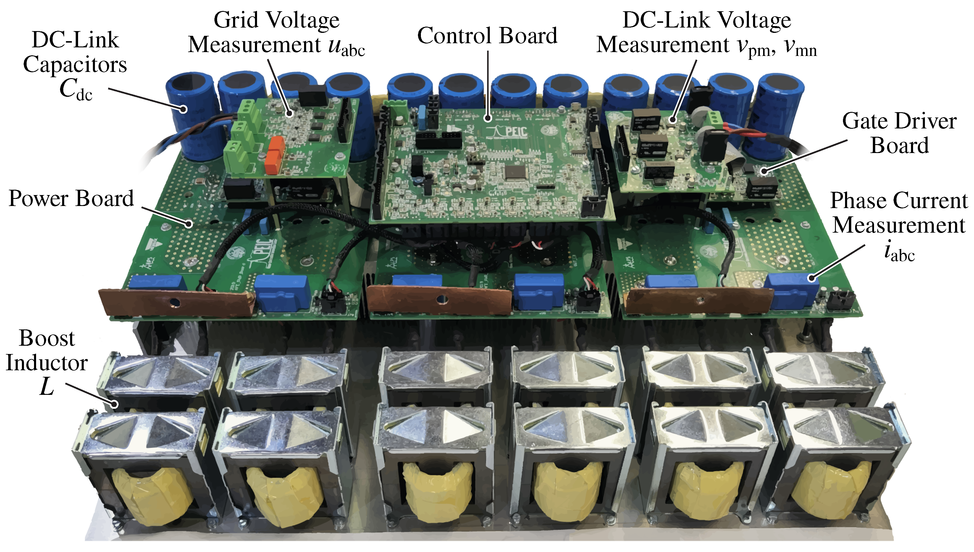
The specifications and the nominal operating conditions of the three-level T-type unidirectional rectifier exploited for the experimental validation are reported in Table 1. It is worth noting that this converter has been designed as the active front-end stage of an electric vehicle ultra-fast battery charger [16,39]. The rectifier prototype is illustrated in Figure 11 and consists of two paralleled three-phase 30 k W units, realized for modularity reasons. Nevertheless, only one converter unit is used in the experimental tests, due to the maximum power limitation of the available equipment.
Each converter bridge-leg employs two 650 V Si MOSFETs connected in anti-series (i.e., as 4Q switch) operating at 20 k Hz and two 1200 V Si fast-recovery diodes. Furthermore, the converter boost inductors employ XFlux 60 μ powder cores from Magnetics [40], which are characterized by a soft-saturating B–H characteristic. This feature leads to a current-dependent variable inductance value (see Table 1), which must be taken into account in the control tuning [16]. The detailed characteristics of the inductor design are reported in [39], obtained as a result of the optimization procedure described in [41].
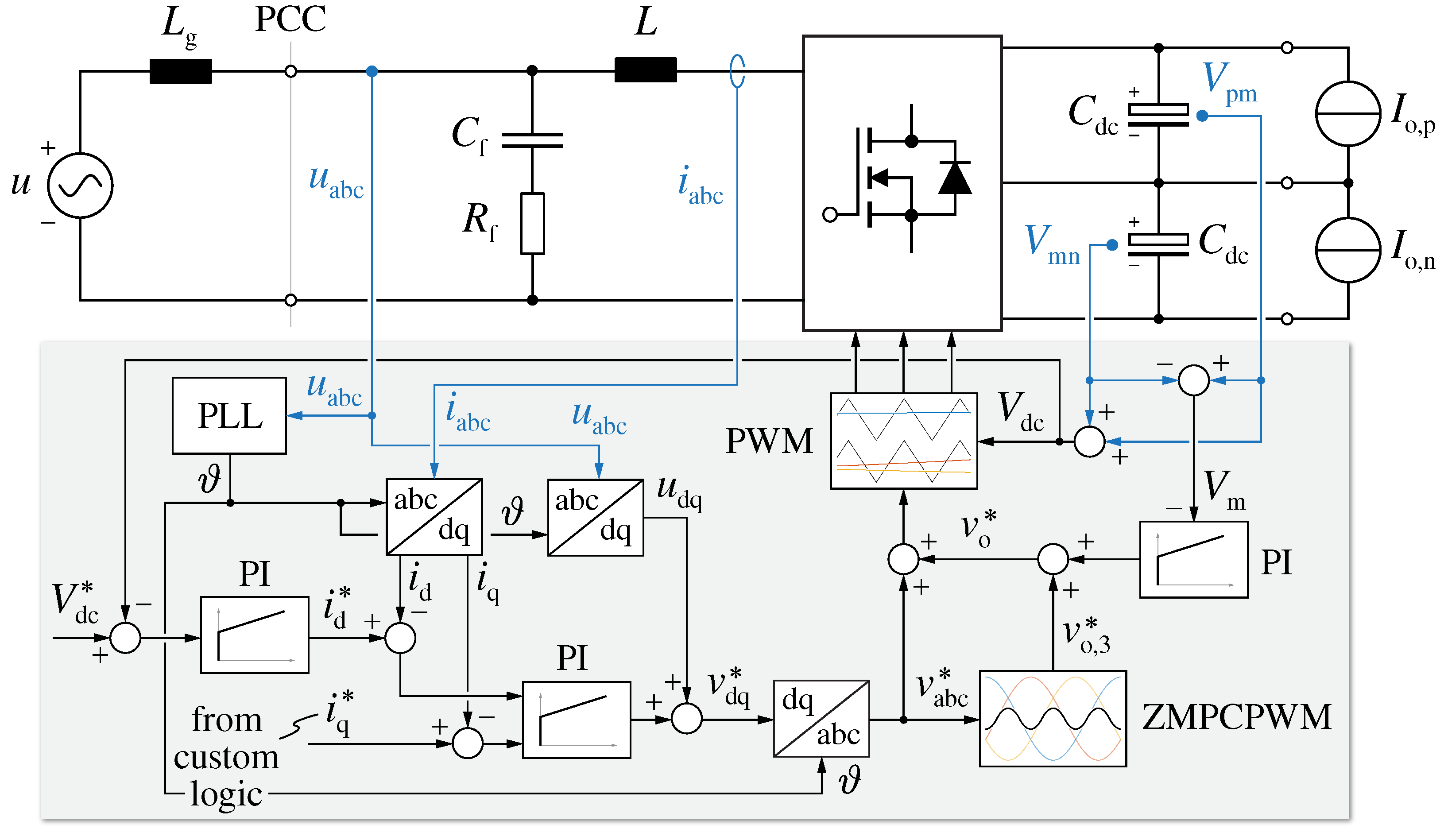
Figure 12 shows a schematic diagram of the adopted experimental setup. The T-type rectifier is connected to a grid emulator (i.e., emulating the 50 Hz , 400 V European low-voltage grid) by means of an L C L filter, consisting of the converter boost inductors (L), filter capacitors ( C f = 15   μ F ) equipped with series damping resistors ( R f = 0.8   Ω ), and grid-side inductors ( L g = 100   μ H ). The main scope of the L C L filter is to eliminate the switching-frequency harmonic content from the grid currents i g , abc [17,42], so that a lower current total harmonic distortion (THD) is achieved and the converter may comply with grid-code standards [43,44]. Furthermore, the presence of the L C L filter allows isolation of the low-frequency component of the distortion, which depends on the control strategy, from the switching-frequency one, which only depends on the selected modulation scheme, allowing for a proper assessment of the converter closed-loop control performance. In the present case, the values of C f and R f are selected according to [39], and the value of L g is representative of an equivalent inner grid impedance of ≈0.02 pu. On the DC-side, the converter is connected to two independent electronic loads, which emulate the rectifier split DC-link loads. The measurements are performed both with a Teledyne LeCroy 500 MHz, 12-bit, 10 GS/s, 8-channel oscilloscope (i.e., employing isolated high-voltage differential probes for voltage measurements and standard current probes for current measurements), and with an HBM GEN4tB 2 MS/s data acquisition system, leveraging current and voltage sensors with high rated accuracy (i.e., < 0.1 ). In particular, the latter approach has been exploited to automatically map the rectifier performance over its complete operating region.

3.1. Multi-Loop Control Scheme

The rectifier is controlled with the full-digital multi-loop control strategy reported in [16], where the detailed description and tuning of all loops is provided. A conventional voltage-oriented dq current control scheme is adopted [17,45,46,47], complemented by a DC-link voltage loop, tracking the desired DC-link voltage value V dc , and a DC-link mid-point voltage balancing loop, ensuring limited steady-state and dynamical V m voltage deviation. A simplified block diagram of the complete system and the adopted control strategy is provided in Figure 13.
The voltages at the point of common coupling (PCC) are measured to achieve the reference frame synchronization with the grid by means of a phase locked loop (PLL) [48,49]. The measured grid voltages are then fed forward in the current control loop, to unburden the integral part of the PI regulator. Even though the digital sampling and update process is performed once per switching/control period, the i abc current feedback values are obtained by means of oversampling (32 samples per control period) and averaging, to enhance the measurement quality around the current zero-crossings. In fact, traditional synchronous/asynchronous sampling approaches do not provide the correct average current value when discontinuous conduction mode (DCM) takes place [21,50], thus affecting the current control accuracy and leading to increased low-frequency distortion. The DC-link voltage loop controls the active power transfer of the rectifier and therefore provides the reference to the d-axis current control loop. The q-axis current i q , instead, is typically controlled to compensate the reactive power injected by the filter capacitors C f (i.e., to ensure unity power factor operation at the PCC), nevertheless it can be set to any value that complies with the converter-side power factor angle limitations of the rectifier (see Section 2.4), being φ = tan 1 ( i q / i d ) . Finally, the DC-link mid-point voltage balancing loop ensures V pm V mn at all times, acting on the zero-sequence voltage v o injection [9,14,15,16,51]. In particular, this control loop theoretically does not interfere with the others, as v o affects neither the active power transfer nor the phase current formation process (see Section 2.1.1). Furthermore, the measured V m is passed through a moving average filter operated at 3 f , so that the control loop does not react to the possibly occurring low-frequency mid-point voltage oscillation.
In practice, the complete converter multi-loop control strategy is implemented on a STM32G474VE MCU from ST Microelectronics [52] with an interrupt service routine running at f s = 20   k Hz .

3.2. Steady-State Performance Evaluation

The most significant rectifier waveforms in steady-state operation are illustrated in Figure 14, where the grid voltages u abc , the converter-side currents i abc and the grid-side (i.e., filtered) currents i g , abc are shown for V dc = 800   V , φ = 0 and different values of transferred power. It is observed that the grid-side current quality improves with the rectifier loading. For instance, at 10% of the rated power (see Figure 14b) the converter-side current ripple amplitude becomes comparable to the current peak value, therefore leading to marked low-frequency zero-crossing distortion that bypasses the filter capacitor and appears in the grid-side currents. Even though the distortion at light load may seem large, the pronounced DCM operation of unidirectional rectifiers typically leads to much higher distortion levels [21]. In the present case, the pseudo-sinusoidal shape of the currents is maintained thanks to the adopted current oversampling and averaging strategy, the high current control loop bandwidth and the feed-forward contributions reported in Figure 13 [16]. At 50% and 100% of the rated power (see Figure 14c,d the quality of both converter-side and grid-side currents improves substantially, as the relative amplitude of the current ripple decreases and the zero-crossing distortion related to DCM operation is mostly eliminated by the current control loop [16].
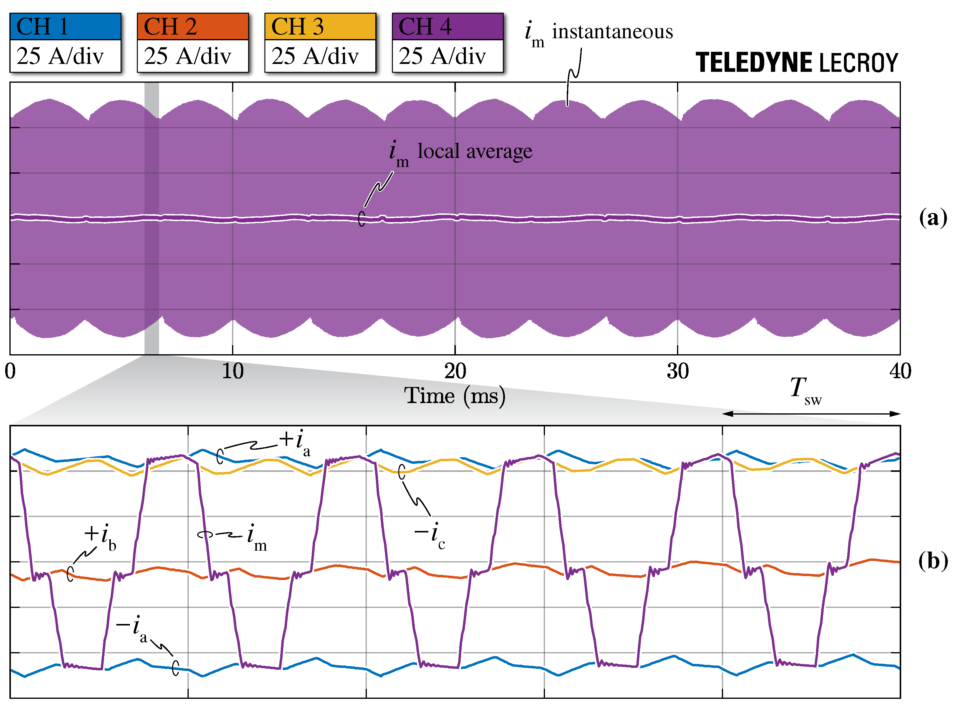
Both instantaneous and local average values of the DC-link mid-point current i m for V dc = 800   V ( M 0.81 ), φ = 0 and P = 30   k W are illustrated in Figure 15, where a focus is also provided in (b). Although the instantaneous value of i m jumps between the converter-side phase current values ± i a , ± i b , ± i c and 0 (i.e., visible from the current envelopes), the local average value of i m 
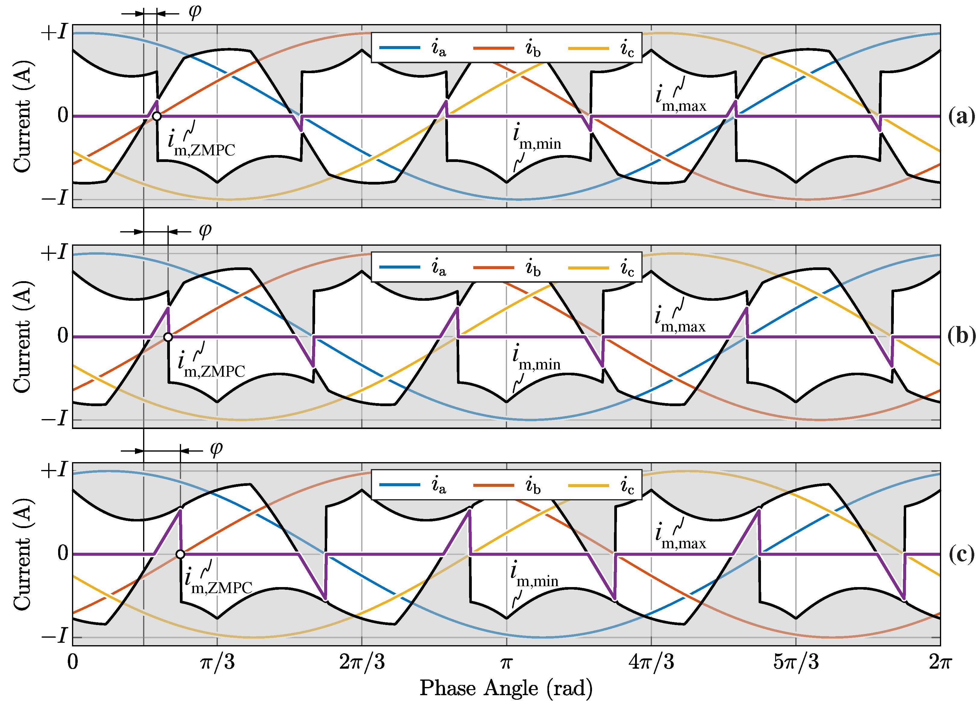
remains approximately 0 along the complete grid period, due to the adopted zero-mid-point current modulation (ZMPCPWM) strategy. A focus of the instantaneous values of i a , i b , i c and i m towards the end of current sector Ⓘ is provided in 
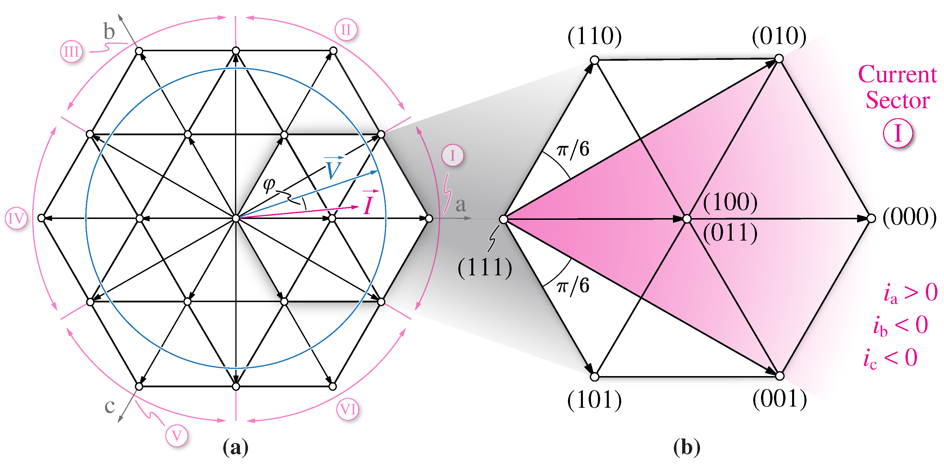
Figure 15b, where the mid-point current is shown to jump between + i a (state 100), i a (state 011), + i b (state 010) and i c (state 110), as expected from space vector theory (see Figure 3b).
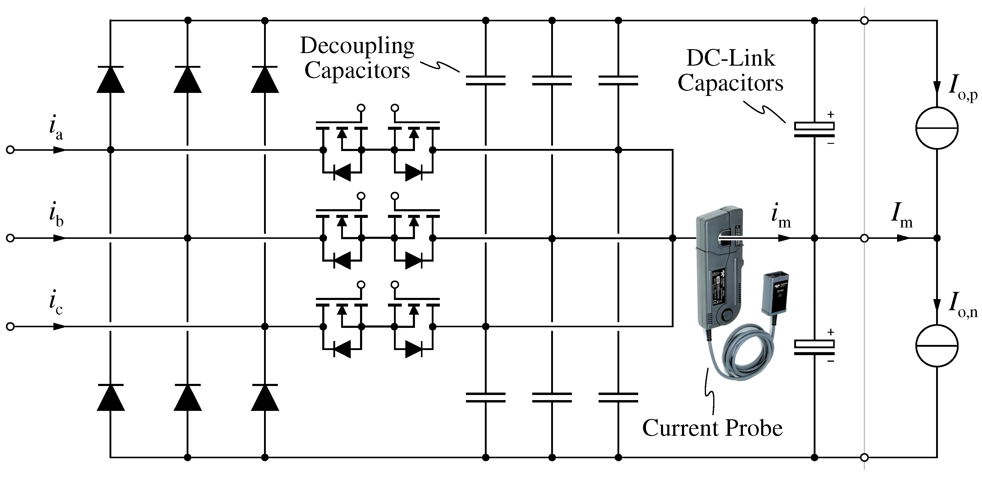
It is worth noting that the measurement of the instantaneous mid-point current value is not common in the literature (i.e., the only case known to the authors is [53]), as it represents a challenging task to achieve. In practice, the current measurement must be placed within the commutation loop of all bridge-legs, thus negatively affecting the switching performance of the rectifier. In the present case, the measurement of i m has been achieved by placing the current probe between the bridge-leg decoupling capacitors (i.e., 220 n F ceramic capacitors) and the DC-link capacitors (i.e., 4080 μ F electrolytic capacitors), as schematically illustrated in Figure 16. Even though the decoupling capacitors are placed in parallel to the DC-link capacitors, their small capacitance value does not substantially affect the mid-point current, especially considering the relatively low switching frequency of the rectifier.
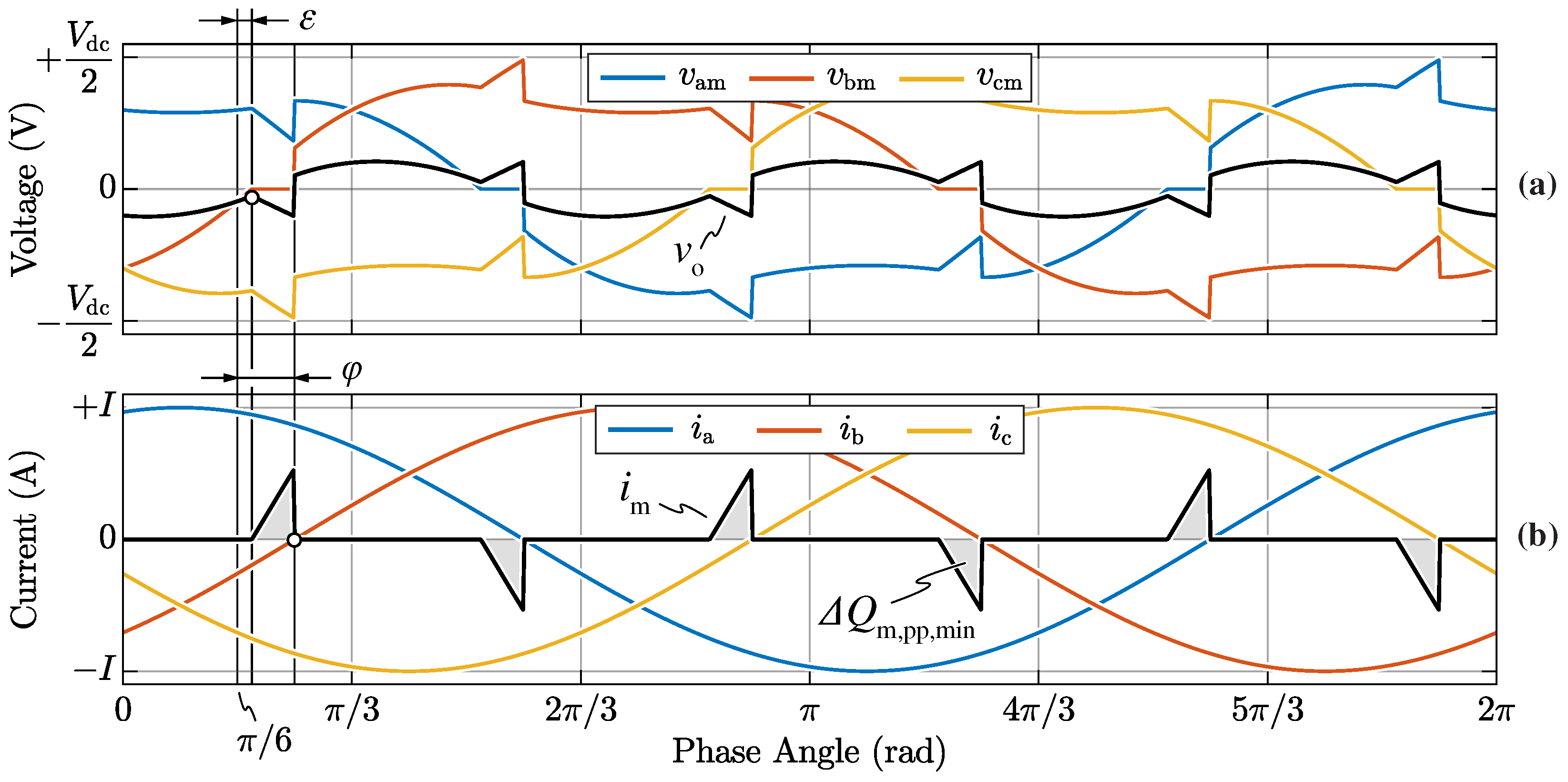
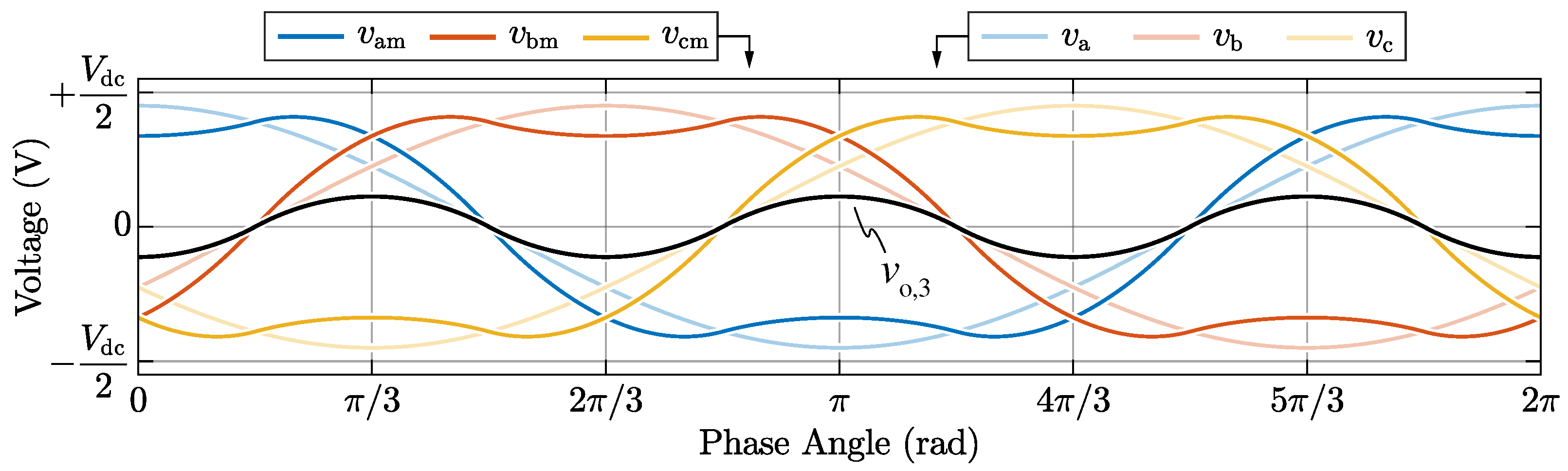
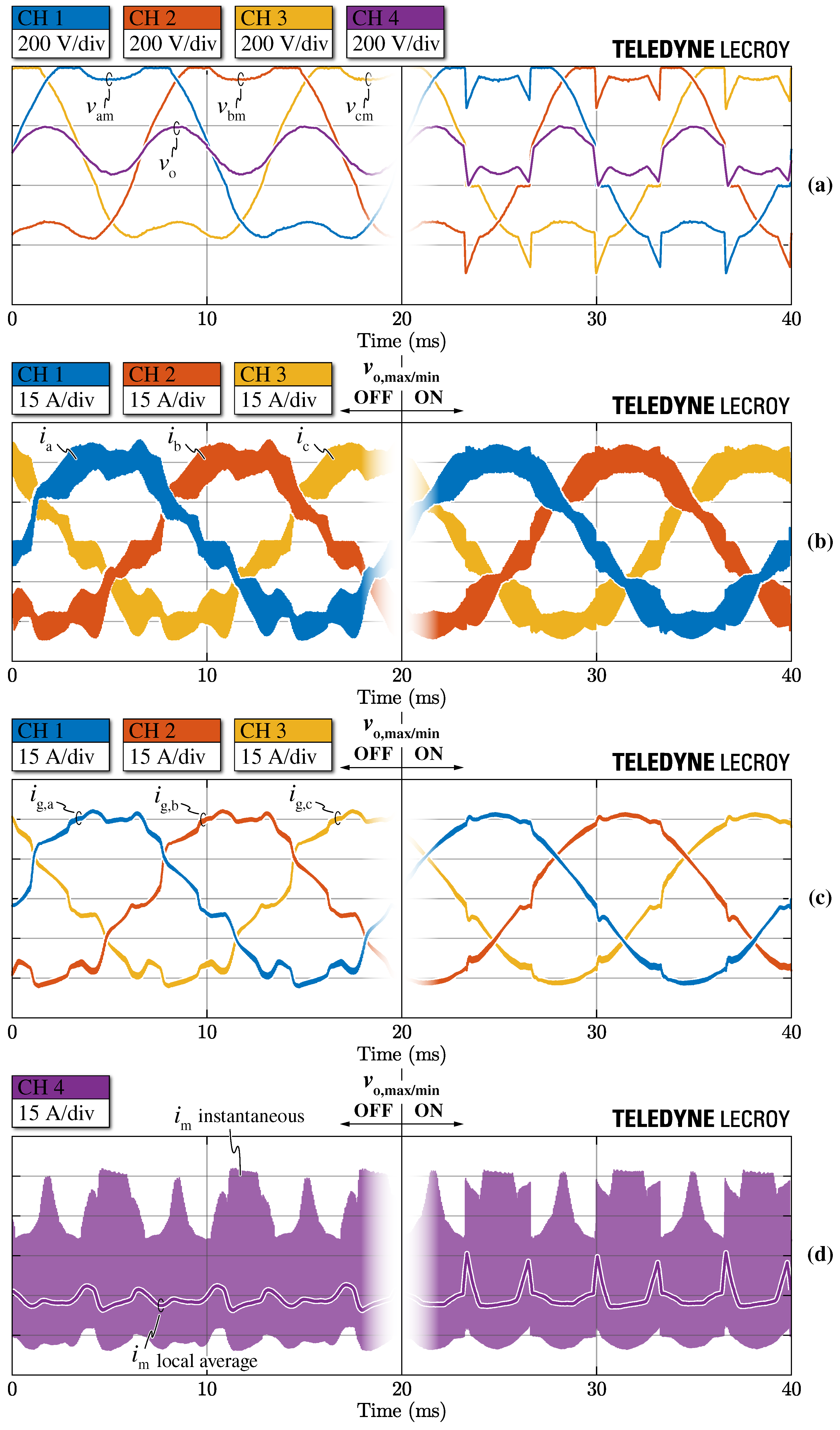
Figure 17 and Figure 18 show the most relevant rectifier waveforms under non-unity power factor operation and constant zero-sequence voltage injection, respectively. In particular, the reference bridge-leg voltages v am , v bm , v cm , the reference zero-sequence voltage v o , the converter-side currents i abc , the grid-side currents i g , abc and the DC-link mid-point current i m are shown for V dc = 800   V and S = 15   k VA . Furthermore, the effect of the zero-sequence voltage saturation v o , max / min on all measured quantities is highlighted by comparing the results with a conventional control implementation (i.e., with no saturation acting on v o ). It is worth noting that v am , v bm , v cm and v o are obtained from separate digital-to-analog converters (DACs) of the MCU (i.e., with a 0– 3.3   V scale) and are thus rescaled in Figure 17a and Figure 18a.
Figure 17 shows the operation of the rectifier with φ = 15 . In particular, Figure 17c highlights that non-unity power factor operation generates a large zero-crossing distortion if no zero-sequence voltage saturation is implemented. The enforcement of v o , max / min , in fact, allows the rectifier to correctly apply the desired bridge-leg voltage values even when the phase currents are phase-shifted with respect to the reference voltages, as described in Section 2. Consequently, undistorted operation under non-unity power factor is achieved. Furthermore, Figure 17d shows that by saturating the zero-sequence voltage, a larger mid-point current local average i m and thus a higher DC-link mid-point peak-to-peak charge ripple Δ Q m , pp are obtained. This is because, to ensure the undistorted operation of the rectifier, the applied zero-sequence voltage v o departs from the ideal v o , 3 value introduced by the ZMPCPWM (see Figure 17a). It is also worth observing that the local average of i m obtained experimentally is in good agreement with the simulated waveforms reported in Figure 7 and Figure A4b.
The rectifier waveforms with a constant zero-sequence voltage v o = 0.15 V dc / 2 added to v o , 3 (i.e., ZMPCPWM injection) are shown in Figure 18. This injection emulates the converter performance under unbalanced split DC-link loading, i.e., when a constant mid-point current periodical average I m = I o , n I o , p is required. This is highlighted in Figure 18d, where the injection of a positive zero-sequence voltage is shown to generate a negative value of mid-point periodical average I m , as expected from theoretical considerations. Additionally in this case larger i m and Δ Q m , pp ripple values are obtained when the v o , max / min saturation is enabled. Figure 18c shows that the zero-sequence voltage saturation v o , max / min allows substantial improvement of the phase current waveforms. Nevertheless, in this case the zero-crossing distortion cannot be completely avoided, since the injection of the constant zero-sequence voltage contribution increases the amplitude of the converter-side current ripple (see Figure 14c for comparison), which widens the DCM window around the current zero-crossings and leads to higher distortion. It is worth noting that this issue can be greatly reduced in practice by independently controlling the two anti-series mid-point switches, such that the free-wheeling of the current through the mid-point is always possible [26]. In fact, even though in the present case the two anti-series switches are supplied by independent gate drivers, they receive equal PWM signals, greatly simplifying the modulation and the control of the rectifier. It should be pointed out that the low-frequency distortion would mostly disappear at full load (i.e., P = 30   k W ), due to the lower ratio between the current ripple and the current peak. However, this condition could not be tested, due to the power limitations of the adopted electronic loads.

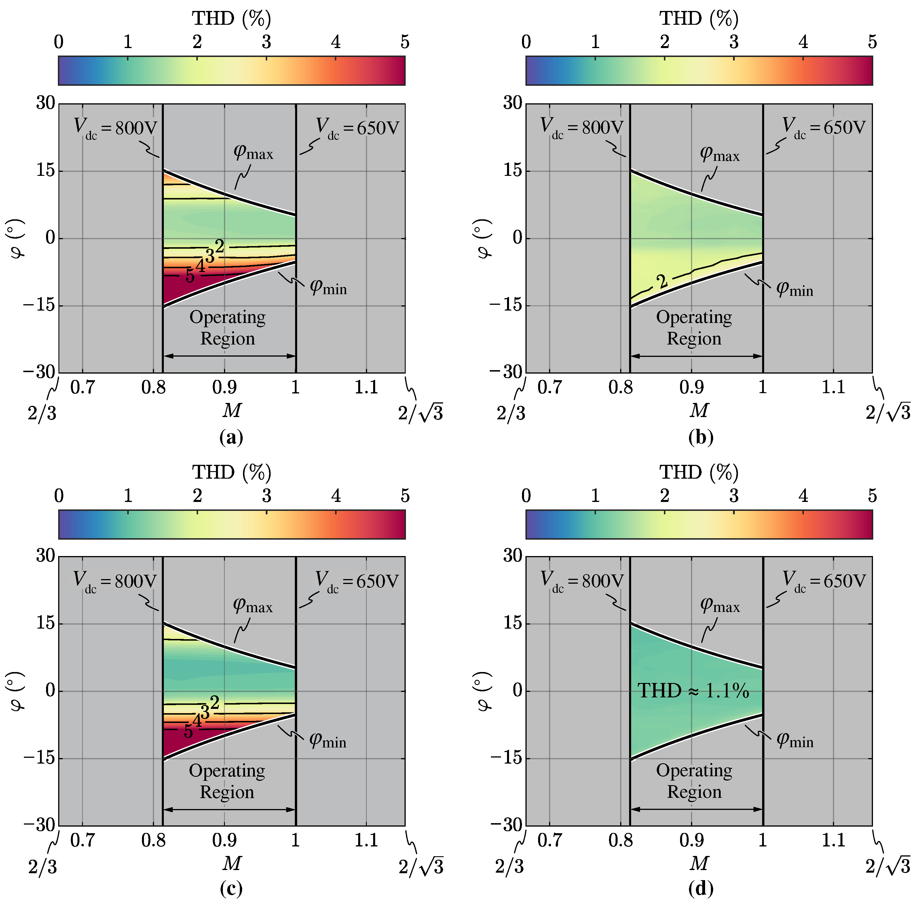
3.2.1. Total Harmonic Distortion (THD)

The grid-side current total harmonic distortion (THD) is defined as
THD = I g , RMS 2 I g , 1 , RMS 2 I g , 1 , RMS
where I g , RMS is the total RMS value of the grid-side current and I g , 1 , RMS is the RMS value of the grid current first harmonic.
The rectifier performance is mapped over the complete modulation index M and converter-side power factor angle φ operating region, both at 50% and 100% of the nominal apparent power (i.e., S = 30   k VA ). The results are shown in Figure 19, where the THD performance obtained with and without v o , max / min saturation are compared. As expected from Figure 14, the quality of the grid-side current improves at higher load levels, as the zero-crossing distortion is reduced. Moreover, by enforcing the zero-sequence voltage saturation, the THD lies below the conventional 5% limit (i.e., required by grid standards [44]) for all operating points, which is not the case when v o , max / min is disabled. Finally, it is observed that the THD values are not symmetrical with respect to φ , resulting in worse distortion for φ < 0 (i.e., capacitive operation). The main explanation resides in the fact that the zero-sequence voltage saturation modifies the current ripple shape and amplitude, leading to a wider DCM operation around the zero-crossings for negative values of φ .

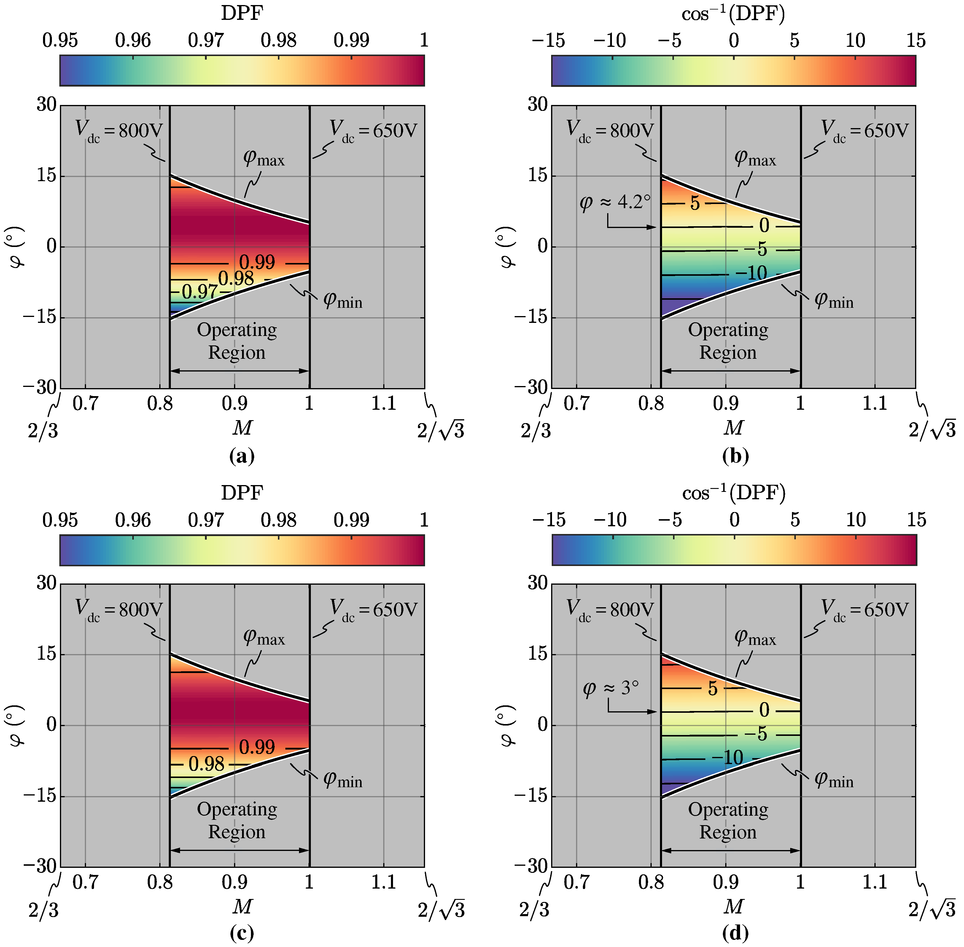
3.2.2. Displacement Power Factor (DPF)

The displacement power factor (DPF) of the rectifier is defined as
DPF = cos U I g = P S
where U and I g are the phase angles of the grid voltage vector (i.e., measured at the PCC) and the grid current vector, respectively. It is worth noting that DPF φ , as the grid-side converter current also includes the filter capacitor current contribution. The experimental DPF is illustrated in Figure 20a,c for 50% and 100% of the nominal apparent power (i.e., S = 30   k VA ). In both cases, the zero-sequence voltage saturation is enabled.
For a better understanding of the phase-shift between U and I g , the DPF angle (i.e., cos 1 ( DPF ) ) is shown in Figure 20b,d, where a positive value indicates a lagging power factor (i.e., inductive behavior) and a negative value indicates a leading power factor (i.e., capacitive behavior). It can be observed that the current flowing into the filter capacitor C f is completely compensated for φ 4.2 at 50% of the rated power and φ 3 at 100% of the rated power, as expected from basic theoretical considerations.

3.2.3. Maximum Mid-Point Current ( I m , max )

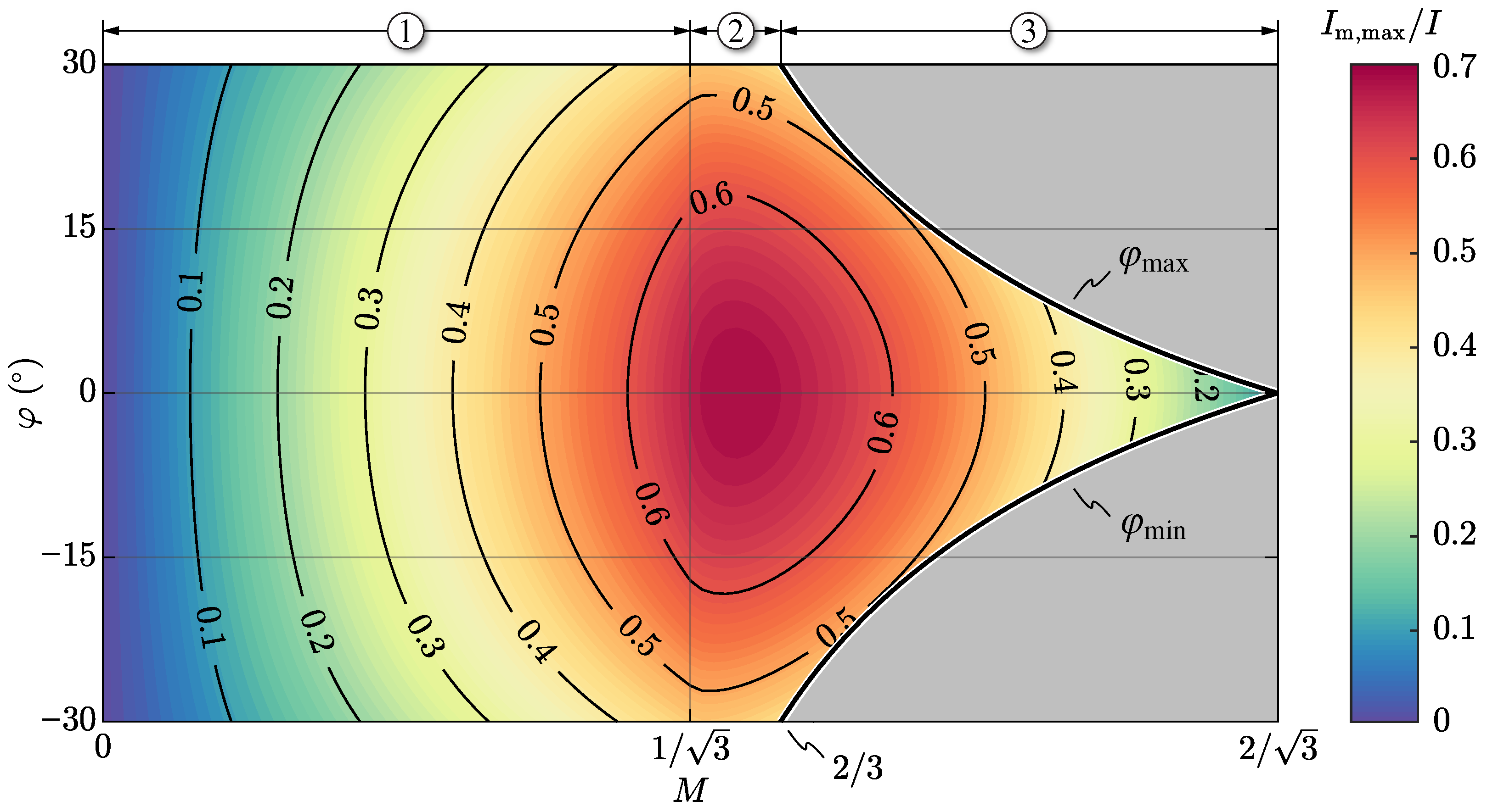
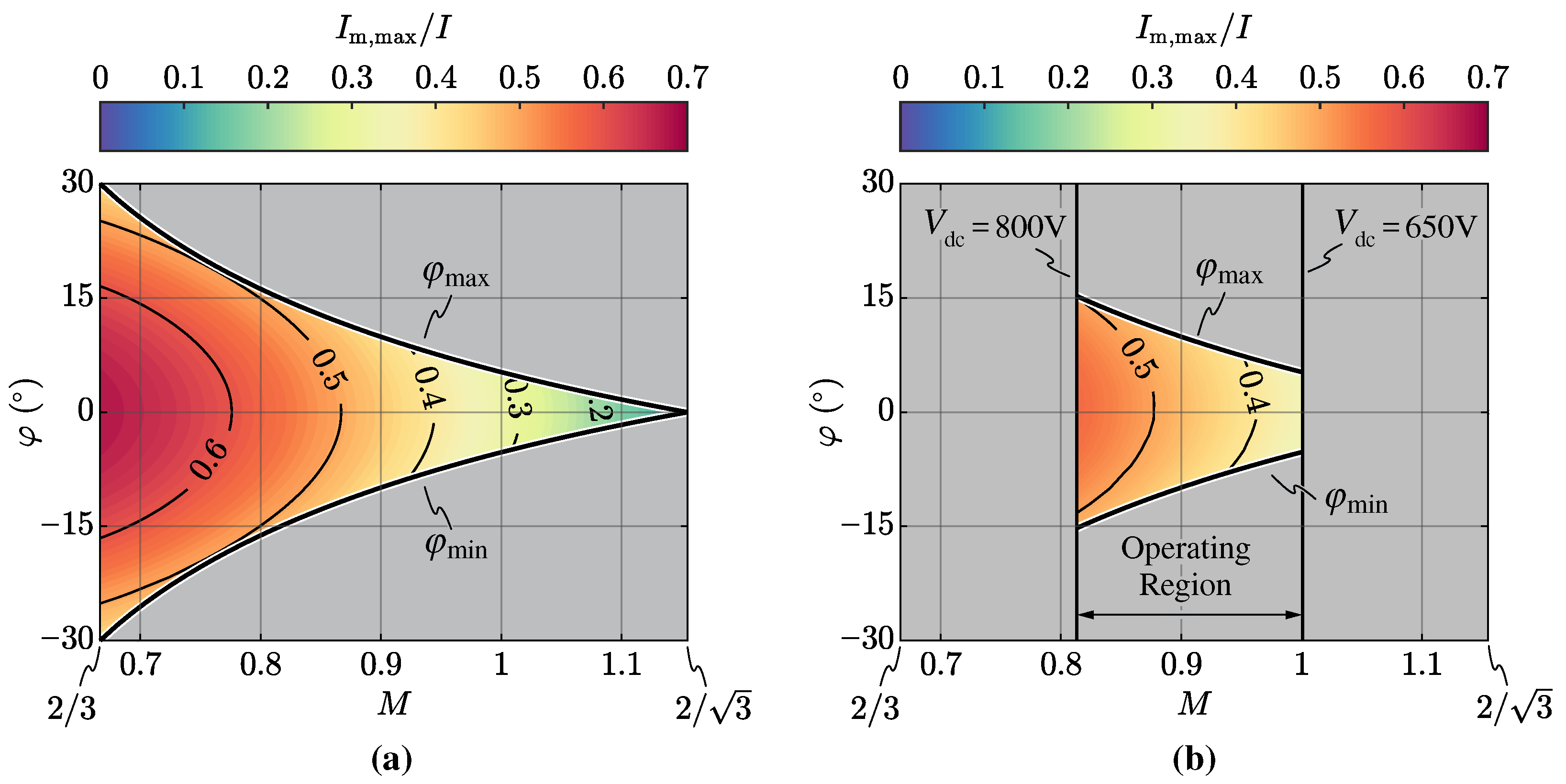
The maximum DC-link mid-point current capability of the rectifier ( I m , max ) is assessed experimentally by operating the converter at 50% of the rated apparent power (i.e., S = 15   k VA ) and injecting a zero-sequence voltage equal to v o , min . The results are illustrated in Figure 8b in Section 2.5, where they are normalized with respect to the converter-side peak current value I. It is observed that the theoretical and the experimental results are in close agreement, achieving a maximum deviation of 5% over the complete operating range of the rectifier. Therefore, the analytical I m , max formulas derived in Appendix A can be considered successfully verified.

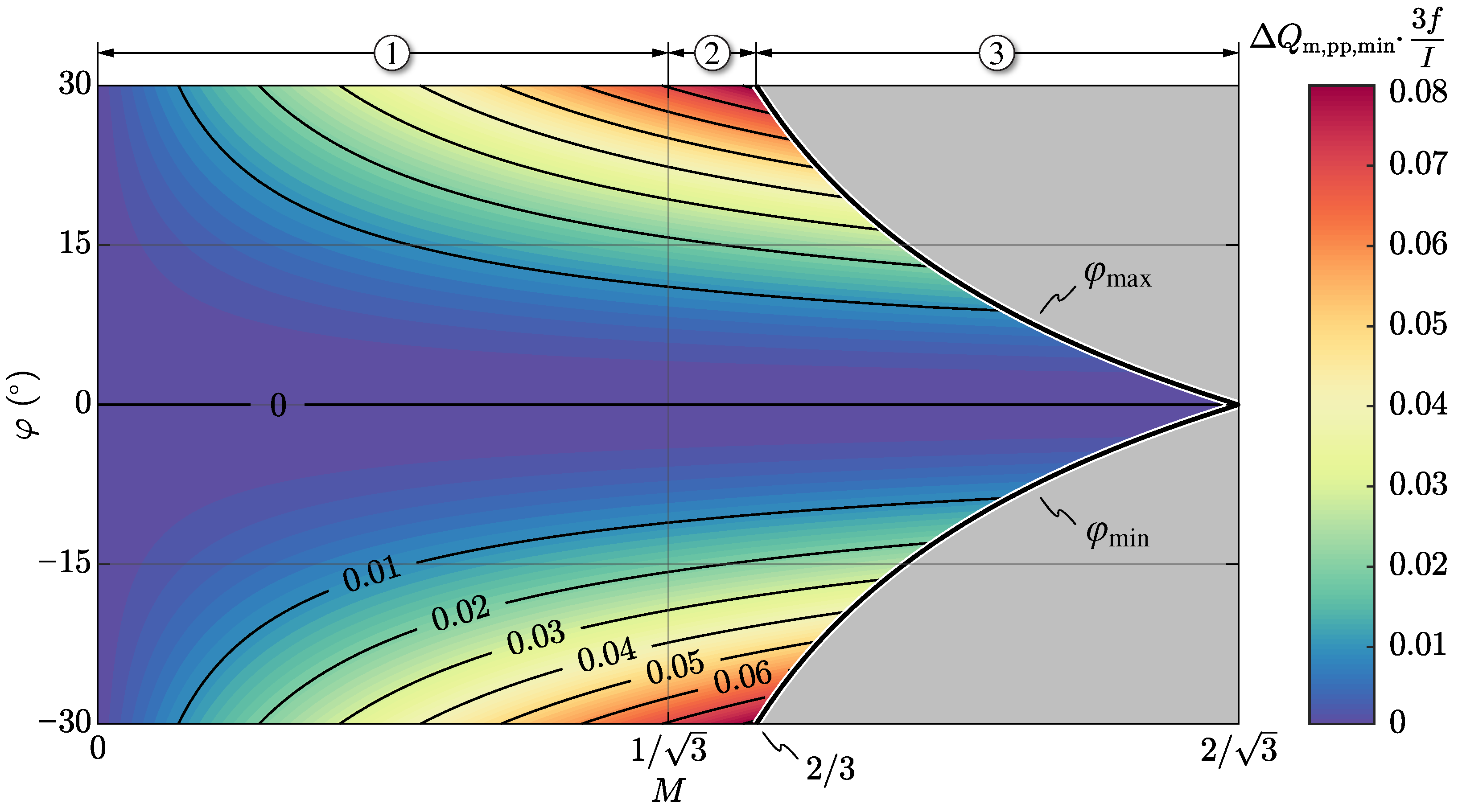
3.2.4. Minimum Mid-Point Charge Ripple ( Δ Q m , pp , min )

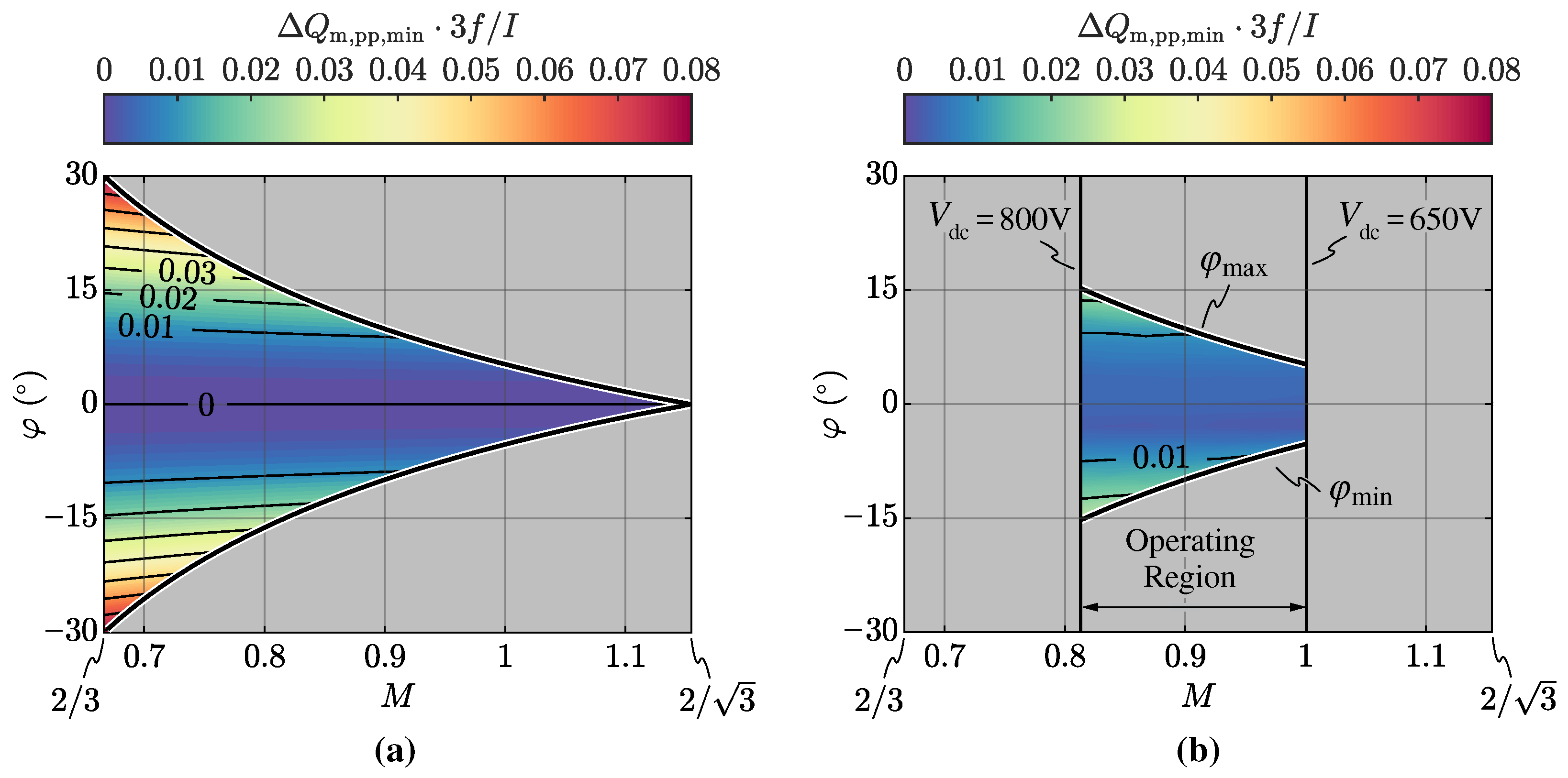
The minimum DC-link mid-point peak-to-peak charge ripple Δ Q m , pp , min is assessed experimentally by operating the converter at 100% of the rated apparent power (i.e., S = 30   k VA ), injecting the zero-sequence voltage component v o , 3 defined by ZMPCPWM and saturating it according to the v o , max / min limits. In particular, the mid-point charge is obtained in post-processing as the integral of the measured mid-point current i m . The results are illustrated in Figure 10b in Section 2.6, where they are normalized with respect to the converter-side peak phase current I and three-times the grid frequency 3 f . Additionally in this case, the theoretical and the experimental results are in close agreement; however, the value Δ Q m , pp , min obtained experimentally does not reach 0 for φ = 0 . This is mainly due to the converter-side current not being perfectly sinusoidal, as it features a slight zero-crossing distortion that yields a non-zero mid-point current local average (see Figure 15). Nevertheless, Δ Q m , pp , min = 0 can never be achieved in practice, as the switching-frequency mid-point current ripple (i.e., neglected in the theoretical model) yields a non-zero charge ripple: theoretical and experimental results at φ = 0 would only coincide for f sw = . Overall, the analytical Δ Q m , pp , min formula derived in Appendix B can be considered successfully verified, achieving best estimation accuracy for systems with f sw f (i.e., with high pulse ratios).

4. Conclusions

This paper has presented a comprehensive analysis and performance assessment of three-phase three-level unidirectional rectifiers under non-unity power factor operation and unbalanced split DC-link loading.
The complete analysis applies to all three-level unidirectional rectifiers and thus features a wide range of applications, e.g., active front ends for the supply of variable-speed drives, uninterruptible power supply systems, battery chargers, data centers and high-power DC loads. In particular, the ability to operate under non-unity power factor is becoming a desired feature of modern rectifiers, as distribution system operators worldwide are starting to charge end consumers for the excess reactive energy injected/withdrawn into/from the grid. In this scenario, properly controlled unidirectional rectifiers could support the reactive energy flows and potentially substitute traditional power factor correction capacitor banks, without requiring new or additional hardware. Furthermore, the ability to operate under unbalanced split DC-link loading is necessary when separate loads are connected to the rectifier DC-link halves, which is typically the case for modular high-power converters (e.g., the DC/DC stage of electric vehicle DC fast chargers).
Therefore, this paper has focused on analyzing, improving and extending the operation of three-phase three-level unidirectional rectifiers. First, the operational basics of three-level rectifiers have been recalled and the theoretical operating limits of the converter in terms of zero-sequence voltage, modulation index, power factor angle, DC-link mid-point current and minimum DC-link mid-point charge ripple have been derived. A unified carrier-based pulse-width modulation (PWM) approach aiming for the undistorted operation of the rectifier across all feasible operating conditions has been proposed, de facto enabling the converter operation under non-unity power factor and unbalanced split-DC-link loading. This approach, uniquely based on restraining (i.e., saturating) the zero-sequence voltage within its feasible limits, has been described in detail and its effects on the DC-link mid-point current generation have been investigated. Furthermore, novel analytical expressions have been derived in the Appendix, defining the rectifier maximum mid-point current capability (i.e., directly linked to the converter DC-link load unbalance) and the minimum peak-to-peak DC-link mid-point charge ripple (i.e., allowing for the straightforward sizing of the DC-link capacitance value) over the complete converter operating region. Finally, the theoretical analysis has been successfully verified on a digitally controlled 30 k W T-type rectifier prototype operating at 20 k Hz . The input phase current total harmonic distortion (THD), the maximum mid-point current capability and the minimum mid-point peak-to-peak charge ripple have been experimentally assessed across all rectifier operating points, demonstrating excellent performance and a high-level of agreement with the analytical predictions.

Author Contributions

Conceptualization, D.C.; methodology, D.C.; software, M.G., E.B.; validation, D.C., M.G., E.B. and F.M.; formal analysis, D.C.; investigation, D.C.; resources, F.M and R.B.; data curation, D.C., M.G., E.B. and F.M.; writing–original draft preparation, D.C.; writing–review and editing, D.C., M.G., E.B., F.M. and R.B; visualization, D.C.; supervision, F.M. and R.B; project administration, F.M. and R.B.; funding acquisition, R.B. All authors have read and agreed to the published version of the manuscript.

Funding

This research was funded by the Power Electronics Innovation Center (PEIC), Politecnico di Torino.

Conflicts of Interest

The authors declare no conflict of interest.

Appendix A. Analytical Derivation of the Mid-Point Current Limits

The boundaries of the mid-point current periodical average I m can be derived averaging the maximum and minimum feasible envelopes of i m along the grid period, i.e., integrating (24) over 2 π / 3 . In particular, being the integrals of i m , max and i m , min identical but with opposite sign, the I m limits are symmetrical:
I m , max = I m , min = 3 π V dc 0 2 π / 3 [ x = a , b , c v x | i x | + v o , min x = a , b , c | i x | ] d ϑ .
Figure A1. Zero-sequence voltage limits v o , max , v o , min and mid-point current local average limits i m , max , i m , min for (a) M = 0.5 (region ➀), (b) M = 0.6 (region ➁) and (c) M = 0.7 (region ➂) assuming φ = 10 . The focus is on 0 ϑ π / 3 to highlight the most relevant angle definitions for the analytical calculations (i.e., φ , δ , γ ).
Energies 14 05280 g0a1
Due to the 2 π / 3 periodicity of the first term, its integral is null, thus resulting in
I m , max = 3 π V dc 0 2 π / 3 v o , min | i a | + | i b | + | i c | d ϑ .
To ease the solution of (A2), it is worth observing that i m , max for 0 ϑ π / 3 is equal to i min for π / 3 ϑ 2 π / 3 (see Figure 6 and Figure 7). Therefore, the integration interval may be restricted to ϑ [ 0 , π / 3 ] by considering both maximum and minimum i m envelopes. A highlight of the waveforms within the selected integration interval is provided in Figure A1.
Therefore, leveraging the v o , min definition and the signs of i a , i b , i c inside the considered averaging window, different I m , max expressions are obtained depending on the value of the modulation index. In particular, three main regions can be defined, as illustrated in Figure A2: region ➀ with M < 1 / 3 , region ➁ with 1 / 3 M 2 / 3 (i.e., the transition region) and region ➂ with M > 2 / 3 . The current and voltage waveforms for regions ➀, ➁ and ➂ are reported in Figure A1a–c, respectively.
Figure A2. Overview of the modulation index regions ➀, ➁ and ➂ on the space vector diagram, focusing on 0 ϑ π / 3 . The transition region ➁ is highlighted in grey and the most significant angle definitions for the analytical calculations are indicated (i.e., ϑ , δ , γ ).
Energies 14 05280 g0a2
The expressions of I m , max are therefore:
I m , max , = 6 π V dc [ 0 π / 6 + φ i a v a d ϑ π / 6 + φ π / 3 i c v b d ϑ 0 π / 6 + φ i a v b d ϑ + π / 6 + φ π / 3 i c v c d ϑ ] ,
valid for M < 1 / 3 ,
I m , max , = 6 π V dc [ 0 π / 6 + φ i a v b d ϑ π / 6 + φ π / 3 δ i c V dc 2 v a d ϑ + π / 3 δ π / 3 i c v c d ϑ + + 0 δ i a v a d ϑ + δ π / 6 + φ i a V dc 2 + v c d ϑ π / 6 + φ π / 3 i c v b d ϑ ] ,
valid for 1 / 3 M 2 / 3 , and
I m , max , = 6 π V dc [ 0 π / 6 + φ i a V dc 2 + v c d ϑ π / 6 + φ π / 3 γ i c v b d ϑ π / 3 γ π / 3 i c V dc 2 + v c d ϑ + + 0 γ i a V dc 2 v a d ϑ γ π / 6 + φ i a v b d ϑ π / 6 + φ π / 3 i c V dc 2 v a d ϑ ] ,
valid for M > 2 / 3 . The angles δ , γ are graphically illustrated in Figure A1 and Figure A2, and their expression is obtained by setting v a = v c + V dc / 2 and v a V dc / 2 = v b , respectively, as
δ = π 6 cos 1 1 3 M 1 3 M 2 3 ,
γ = π 3 sin 1 1 3 M M 2 3 .
Finally, substituting (3), (5), (A6), (A7) into (A3)–(A5) and solving the integral terms, the following analytical expressions are obtained:
I m , max , = 3 π I M 4 cos φ π + 3 2 3 φ tan φ
valid for M < 1 / 3 and
I m , max , = I m , max , = 3 π I [ 1 + 1 2 M cos φ 3 M 2 1 1 3 + + M 2 cos φ 3 sin 1 1 3 M π 3 2 2 3 φ tan φ ]
valid for M > 1 / 3 . Expressions (A8) and (A9) are graphically illustrated in Figure A3, where the modulation index regions ➀, ➁ and ➂ are also indicated.
Figure A3. Maximum mid-point current periodical average I m , max (i.e., normalized with respect to the peak phase current I) as a function of the modulation index M and the converter-side power factor angle φ . The three modulation index regions ➀, ➁ and ➂ are indicated.
Energies 14 05280 g0a3
It is worth noting that this analytical derivation extends the approach reported in [16], where the mid-point current periodical average limits are derived uniquely for φ = 0 .

Appendix B. Analytical Derivation of the Minimum Mid-Point Charge Ripple

To identify the minimum value of DC-link mid-point peak-to-peak charge ripple Δ Q m , pp , the zero mid-point current modulation (ZMPCPWM) is considered, therefore the third-harmonic zero-sequence voltage reported in (26) is added to the phase voltage references. Figure A4 shows the zero-sequence voltage v o waveform and the mid-point current local average i m waveform for M = 0.8 and φ = 15 . In particular, it is observed that the zero-sequence voltage saturation occurring for φ 0 causes a deviation of the mid-point current average, which in turn leads to a non-zero Δ Q m , pp .
Figure A4. Zero-sequence voltage v o (a) and mid-point current local average i m (b) for M = 0.8 (region ➂) and φ = 15 . Zero mid-point modulation (ZMPCPWM) is adopted. The most relevant angle definitions for the analytical calculations (i.e., φ , ε ) are indicated.
Energies 14 05280 g0a4
Figure A4 also shows that when ZMPCPWM is adopted, i m 0 within 0 ϑ π / 3 , thus leading to a simplified expression of the mid-point charge ripple:
Δ Q m , pp = 1 2 π f 0 π / 3 i m d ϑ ,
Therefore, due to i m being null for most of the period, the minimum Δ Q m , pp can be calculated by restricting the integration interval to
Δ Q m , pp , min = 1 2 π f π / 6 + ε π / 6 + φ i m d ϑ = 1 π f V dc π / 6 + ε π / 6 + φ [ x = a , b , c v x | i x | + v o , min x = a , b , c | i x | ] d ϑ ,
where i m has been substituted with (16), v o = v o , min within π / 6 + ε ϑ π / 6 + φ , and ε is obtained by setting v o , 3 = v b , as
ε = 1 2 [ φ π 2 + cos 1 1 2 sin φ ] .
Finally, substituting (3), (5), (A12) into (A11) and solving the integral terms, the following analytical expression is obtained:
Δ Q m , pp , min = 3 8 π f I M [ 4 sin 2 φ 2 cos φ sin φ cos 1 sin φ 2 π 2 φ ] ,
valid for the complete modulation index range 0 M 2 / 3 . Expression (A13) is illustrated in normalized form in Figure A5, where the modulation index regions ➀, ➁ and ➂ are also indicated.
Figure A5. Minimum DC-link mid-point charge ripple Δ Q m , pp (i.e., normalized with respect to the peak phase current I and three-times the grid frequency 3 f ) as a function of the modulation index M and the converter-side power factor angle φ . The three modulation index regions ➀, ➁ and ➂ are indicated.
Energies 14 05280 g0a5

References

  1. Kolar, J.W.; Friedli, T. The Essence of Three-Phase PFC Rectifier Systems—Part I. IEEE Trans. Power Electron. 2013, 28, 176–198. [Google Scholar] [CrossRef]
  2. Friedli, T.; Hartmann, M.; Kolar, J.W. The Essence of Three-Phase PFC Rectifier Systems—Part II. IEEE Trans. Power Electron. 2014, 29, 543–560. [Google Scholar] [CrossRef]
  3. Teichmann, R.; Bernet, S. A Comparison of Three-Level Converters versus Two-Level Converters for Low-Voltage Drives, Traction, and Utility Applications. IEEE Trans. Ind. Appl. 2005, 41, 855–865. [Google Scholar] [CrossRef]
  4. Schweizer, M.; Friedli, T.; Kolar, J.W. Comparative Evaluation of Advanced Three-Phase Three-Level Inverter/Converter Topologies Against Two-Level Systems. IEEE Trans. Ind. Electron. 2013, 60, 5515–5527. [Google Scholar] [CrossRef]
  5. Cittanti, D.; Guacci, M.; Mirić, S.; Bojoi, R.; Kolar, J.W. Comparative Evaluation of 800V DC-Link Three-Phase Two/Three-Level SiC Inverter Concepts for Next-Generation Variable Speed Drives. In Proceedings of the International Conference on Electrical Machines and Systems (ICEMS), Hamamatsu, Japan, 24–27 November 2020; pp. 1699–1704. [Google Scholar] [CrossRef]
  6. Anderson, J.A.; Zulauf, G.; Kolar, J.W.; Deboy, G. New Figure-of-Merit Combining Semiconductor and Multi-Level Converter Properties. IEEE Open J. Power Electron. 2020, 1, 322–338. [Google Scholar] [CrossRef]
  7. Kolar, J.; Drofenik, U.; Zach, F. Current Handling Capability of the Neutral Point of a Three-Phase/Switch/Level Boost-Type PWM (VIENNA) Rectifier. In Proceedings of the 27th Annual IEEE Power Electronics Specialists Conference (PESC), Baveno, Italy, 23–27 June 1996; Volume 2, pp. 1329–1336. [Google Scholar] [CrossRef]
  8. Kolar, J.W.; Drofenik, U.; Zach, F.C. On the Interdependence of AC-Side and DC-Side Optimum Control of Three-Phase Neutral-Point-Clamped (Three-Level) PWM Rectifier Systems. In Proceedings of the International Power Electronics and Motion Control Conference (PEMC), Budapest, Hungary, 2–4 September 1996. [Google Scholar]
  9. Kolar, J.; Zach, F. A Novel Three-Phase Utility Interface Minimizing Line Current Harmonics of High-Power Telecommunications Rectifier Modules. IEEE Trans. Ind. Electron. 1997, 44, 456–467. [Google Scholar] [CrossRef] [Green Version]
  10. Ogasawara, S.; Akagi, H. Analysis of Variation of Neutral Point Potential in Neutral-Point-Clamped Voltage Source PWM Inverters. In Proceedings of the IEEE Industry Applications Conference, Toronto, ON, Canada, 2–8 October 1993; pp. 965–970. [Google Scholar] [CrossRef] [Green Version]
  11. Cittanti, D.; Gregorio, M.; Armando, E.; Bojoi, R. Digital Multi-Loop Control of an LLC Resonant Converter for Electric Vehicle DC Fast Charging. In Proceedings of the IEEE Energy Conversion Congress and Exposition (ECCE), Detroit, MI, USA, 11–15 October 2020; pp. 4423–4430. [Google Scholar] [CrossRef]
  12. Cittanti, D.; Vico, E.; Gregorio, M.; Mandrile, F.; Bojoi, R. Iterative Design of a 60 kW All-Si Modular LLC Converter for Electric Vehicle Ultra-Fast Charging. In Proceedings of the AEIT International Conference of Electrical and Electronic Technologies for Automotive (AEIT AUTOMOTIVE), Turin, Italy, 18–20 November 2020. [Google Scholar] [CrossRef]
  13. Mandrile, F.; Cittanti, D.; Mallemaci, V.; Bojoi, R. Electric Vehicle Ultra-Fast Battery Chargers: A Boost for Power System Stability? World Electr. Veh. J. 2021, 12, 16. [Google Scholar] [CrossRef]
  14. Lai, R.; Wang, F.; Burgos, R.; Boroyevich, D.; Jiang, D.; Zhang, D. Average Modeling and Control Design for VIENNA-Type Rectifiers Considering the DC-Link Voltage Balance. IEEE Trans. Power Electron. 2009, 24, 2509–2522. [Google Scholar] [CrossRef]
  15. Leibl, M. Three-Phase PFC Rectifier and High-Voltage Generator for X-ray Systems. Ph.D. Thesis, ETH Zurich, Zurich, Switzerland, 2017. [Google Scholar] [CrossRef]
  16. Cittanti, D.; Gregorio, M.; Bossotto, E.; Mandrile, F.; Bojoi, R. Full Digital Control and Multi-Loop Tuning of a Three-Level T-Type Rectifier for Electric Vehicle Ultra-Fast Battery Chargers. Electronics 2021, 10, 1453. [Google Scholar] [CrossRef]
  17. Liserre, M.; Blaabjerg, F.; Hansen, S. Design and Control of an LCL-Filter-Based Three-Phase Active Rectifier. IEEE Trans. Ind. Appl. 2005, 41, 1281–1291. [Google Scholar] [CrossRef]
  18. Cittanti, D.; Mandrile, F.; Bojoi, R. Optimal Design of Grid-Side LCL Filters for Electric Vehicle Ultra-Fast Battery Chargers. In Proceedings of the International Universities Power Engineering Conference (UPEC), Turin, Italy, 1–4 September 2020. [Google Scholar] [CrossRef]
  19. Cittanti, D.; Bojoi, R. Modulation Strategy Assessment for 3-Level Unidirectional Rectifiers in Electric Vehicle Ultra-Fast Charging Applications. In Proceedings of the AEIT International Conference of Electrical and Electronic Technologies for Automotive (AEIT AUTOMOTIVE), Turin, Italy, 18–20 November 2020. [Google Scholar] [CrossRef]
  20. European Union Agency for the Cooperation of Energy Regulators (ACER). Report on Distribution Tariff Methodologies in Europe. 2021. Available online: https://documents.acer.europa.eu/Official_documents/Acts_of_the_Agency/Publication/ACER%20Report%20on%20D-Tariff%20Methodologies.pdf (accessed on 14 August 2021).
  21. Leibl, M.; Kolar, J.W.; Deuringer, J. Sinusoidal Input Current Discontinuous Conduction Mode Control of the VIENNA Rectifier. IEEE Trans. Power Electron. 2017, 32, 8800–8812. [Google Scholar] [CrossRef]
  22. Lee, J.S.; Lee, K.B. A Novel Carrier-Based PWM Method for Vienna Rectifier With a Variable Power Factor. IEEE Trans. Ind. Electron. 2016, 63, 3–12. [Google Scholar] [CrossRef]
  23. Wang, F.; Teng, Y.; Yuan, Z.; Xu, J. A Maximum Power Factor of Control Algorithms of Three-Level Vienna Rectifier without Current Distortion at Current Zero-Crossing Point. In Proceedings of the 2016 IEEE 8th International Power Electronics and Motion Control Conference (IPEMC-ECCE Asia), Hefei, China, 22–26 May 2016; pp. 2325–2331. [Google Scholar] [CrossRef]
  24. Hu, W.; Yu, A.; Lyu, J.; Ding, H.; Lyu, J. Research on Reducing the Input Current Distortion based on PWM Method for Vienna Rectifier with LCL Filter. In Proceedings of the 2017 Chinese Automation Congress (CAC), Jinan, China, 20–22 October 2017; pp. 6634–6639. [Google Scholar] [CrossRef]
  25. Xu, H.; Yao, W.; Shao, S. Improved SVPWM Schemes for Vienna Rectifiers without Current Distortion. In Proceedings of the 2017 IEEE Energy Conversion Congress and Exposition (ECCE), Cincinnati, OH, USA, 1–5 October 2017; pp. 3410–3414. [Google Scholar] [CrossRef]
  26. Molligoda, D.A.; Pou, J.; Gajanayake, C.; Gupta, A. Analysis of the Vienna Rectifier under Nonunity Power Factor Operation. In Proceedings of the 2018 Asian Conference on Energy, Power and Transportation Electrification (ACEPT), Singapore, 30 October–2 November 2018; pp. 1–7. [Google Scholar] [CrossRef]
  27. Molligoda, D.A.; Pou, J.; Ceballos, S.; Satpathi, K.; Sasongko, F.; Gajanayake, C.J.; Gupta, A.K. Current Distortion Mitigation in Grid-Connected Vienna Rectifier During Nonunity Power Factor Operation. In Proceedings of the IECON 2020 The 46th Annual Conference of the IEEE Industrial Electronics Society, Singapore, 18–21 October 2020; pp. 4085–4090. [Google Scholar] [CrossRef]
  28. Burgos, R.; Lai, R.; Pei, Y.; Wang, F.; Boroyevich, D.; Pou, J. Space Vector Modulator for Vienna-Type RectifiersBased on the Equivalence BetweenTwo- and Three-Level Converters: A Carrier-Based Implementation. IEEE Trans. Power Electron. 2008, 23, 1888–1898. [Google Scholar] [CrossRef]
  29. Ding, W.; Zhang, C.; Gao, F.; Duan, B.; Qiu, H. A Zero-Sequence Component Injection Modulation Method With Compensation for Current Harmonic Mitigation of a Vienna Rectifier. IEEE Trans. Power Electron. 2019, 34, 801–814. [Google Scholar] [CrossRef]
  30. Celanovic, N.; Boroyevich, D. A comprehensive study of neutral-point voltage balancing problem in three-level neutral-point-clamped voltage source PWM inverters. IEEE Trans. Power Electron. 2000, 15, 242–249. [Google Scholar] [CrossRef]
  31. Pou, J.; Pindado, R.; Boroyevich, D.; Rodriguez, P. Evaluation of the low-frequency neutral-point voltage oscillations in the three-level inverter. IEEE Trans. Ind. Electron. 2005, 52, 1582–1588. [Google Scholar] [CrossRef]
  32. Wang, C.; Li, Y. Analysis and Calculation of Zero-Sequence Voltage Considering Neutral-Point Potential Balancing in Three-Level NPC Converters. IEEE Trans. Ind. Electron. 2010, 57, 2262–2271. [Google Scholar] [CrossRef]
  33. Wang, J.; Gui, Z.; Wang, P.; Wang, J.; Jiang, W. A Carrier-Based Modulation With Planned Zero Sequence Voltage Injection to Control Neutral Point Voltage for Three-Level Inverter. IEEE Access 2020, 8, 64799–64809. [Google Scholar] [CrossRef]
  34. Chen, F.; Qiao, W.; Wang, H.; Qu, L. A Simple Zero-Sequence Voltage Injection Method for Carrier-Based Pulsewidth Modulation of the Three-Level NPC Inverter. IEEE J. Emerg. Sel. Top. Power Electron. 2021, 9, 4687–4699. [Google Scholar] [CrossRef]
  35. Zhao, W.; Ruan, X.; Yang, D.; Chen, X.; Jia, L. Neutral Point Voltage Ripple Suppression for a Three-Phase Four-Wire Inverter With an Independently Controlled Neutral Module. IEEE Trans. Ind. Electron. 2017, 64, 2608–2619. [Google Scholar] [CrossRef]
  36. Zhang, L.; Shi, D.; Yang, T.; Wang, K.; Tang, Y.; Loh, W.K. Partial Power Processing for Power Decoupling Network in Three-Phase Three-Leg Four-Wire Three-Level T-Type Inverter with Reduced Split DC-Bus Capacitance. IEEE Trans. Ind. Electron. 2021. [Google Scholar] [CrossRef]
  37. Salmon, J. Comparative Evaluation of Circuit Topologies for 1-Phase and 3-Phase Boost Rectifiers Operated with a Low Current Distortion. In Proceedings of the 1994 Proceedings of Canadian Conference on Electrical and Computer Engineering (CCECE), Halifax, NS, Canada, 25–28 September 1994; Volume 1, pp. 30–33. [Google Scholar] [CrossRef]
  38. Dahono, P.; Sato, Y.; Kataoka, T. Analysis and Minimization of Ripple Components of Input Current and Voltage of PWM Inverters. IEEE Trans. Ind. Appl. 1996, 32, 945–950. [Google Scholar] [CrossRef]
  39. Cittanti, D.; Mandrile, F.; Gregorio, M.; Bojoi, R. Design Space Optimization of a Three-Phase LCL Filter for Electric Vehicle Ultra-Fast Battery Charging. Energies 2021, 14, 1303. [Google Scholar] [CrossRef]
  40. Magnetics. 00X6527E060 Datasheet. Available online: https://www.mag-inc.com/Products/Powder-Cores/XFlux-Cores (accessed on 11 May 2021).
  41. Borlo, S.; Cittanti, D.; Gregorio, M.; Mandrile, F.; Musumeci, S. Comparative CCM-DCM Design Evaluation of Power Inductors in Interleaved PFC Stage for Electric Vehicle Battery Chargers. In Proceedings of the International Conference on Clean Electrical Power (ICCEP), Otranto, Italy, 2–4 July 2019; pp. 180–186. [Google Scholar] [CrossRef]
  42. Liserre, M.; Dell’Aquila, A.; Blaabjerg, F. Stability Improvements of an LCL-Filter Based Three-Phase Active Rectifier. In Proceedings of the IEEE Power Electronics Specialists Conference (PESC), Cairns, QLD, Australia, 23–27 June 2002; Volume 3, pp. 1195–1201. [Google Scholar] [CrossRef]
  43. Hoevenaars, T.; LeDoux, K.; Colosino, M. Interpreting IEEE STD 519 and Meeting its Harmonic Limits in VFD Applications. In Proceedings of the IEEE Petroleum and Chemical Industry Conference (PCIC), Houston, TX, USA, 15–17 September 2003; pp. 145–150. [Google Scholar] [CrossRef]
  44. IEEE. IEEE Recommended Practice and Requirements for Harmonic Control in Electric Power Systems; IEEE Std 519-2014; IEEE: Piscataway, NJ, USA, 2014; pp. 1–29. [Google Scholar] [CrossRef]
  45. Blasko, V.; Kaura, V. A Novel Control to Actively Damp Resonance in Input LC Filter of a Three-Phase Voltage Source Converter. IEEE Trans. Ind. Appl. 1997, 33, 542–550. [Google Scholar] [CrossRef]
  46. Jalili, K.; Bernet, S. Design of LCL Filters of Active-Front-End Two-Level Voltage-Source Converters. IEEE Trans. Ind. Electron. 2009, 56, 1674–1689. [Google Scholar] [CrossRef]
  47. Cittanti, D.; Gregorio, M.; Bojoi, R. Digital Multi-Loop Control of a 3-Level Rectifier for Electric Vehicle Ultra-Fast Battery Chargers. In Proceedings of the AEIT International Annual Conference (AEIT), Catania, Italy, 23–25 September 2020. [Google Scholar] [CrossRef]
  48. Blaabjerg, F.; Teodorescu, R.; Liserre, M.; Timbus, A. Overview of Control and Grid Synchronization for Distributed Power Generation Systems. IEEE Trans. Ind. Electron. 2006, 53, 1398–1409. [Google Scholar] [CrossRef] [Green Version]
  49. Limongi, L.R.; Bojoi, R.; Pica, C.; Profumo, F.; Tenconi, A. Analysis and Comparison of Phase Locked Loop Techniques for Grid Utility Applications. In Proceedings of the Power Conversion Conference (PCC), Nagoya, Japan, 2–5 April 2007; pp. 674–681. [Google Scholar] [CrossRef]
  50. Cittanti, D.; Gregorio, M.; Mandrile, F.; Bojoi, R. Full Digital Control of an All-Si On-Board Charger Operating in Discontinuous Conduction Mode. Electronics 2021, 10, 203. [Google Scholar] [CrossRef]
  51. Bel Haj Youssef, N.; Al-Haddad, K.; Kanaan, H.Y. Implementation of a New Linear Control Technique Based on Experimentally Validated Small-Signal Model of Three-Phase Three-Level Boost-Type Vienna Rectifier. IEEE Trans. Ind. Electron. 2008, 55, 1666–1676. [Google Scholar] [CrossRef]
  52. ST Microelectronics. STM32G474VE Datasheet. Available online: https://www.st.com/en/microcontrollers-microprocessors (accessed on 11 May 2021).
  53. Dalessandro, L.; Round, S.D.; Drofenik, U.; Kolar, J.W. Discontinuous Space-Vector Modulation for Three-Level PWM Rectifiers. IEEE Trans. Power Electron. 2008, 23, 530–542. [Google Scholar] [CrossRef]
Figure 1. Schematic overview of typical grid-connected three-phase rectifier configurations supplying electrical loads such as (a) three-phase DC/AC inverters for variable-speed drives (VSDs) or uninterruptible power supplies (UPSs), (b) isolated DC/DC converters for electric vehicle DC fast charging, telecommunication and data center power supplies, lighting systems or induction heating, and (c) non-isolated DC/DC converters for DC distribution systems, high-power DC loads or DC microgrids.
Energies 14 05280 g001
Figure 2. Schematic overview of a three-level rectifier connected to the three-phase grid. The mid-point switches must be bipolar and bidirectional, i.e., 4-quadrant (4Q). A highlight of the possible 4Q switch topologies is provided, namely (a) the T-type, (b) the NPC-type, and (c) the VIENNA-type: switches (b,c) can also be integrated inside the input diode bridge (see [9,37]).
Energies 14 05280 g002
Figure 3. Complete space vector diagram of a three-phase three-level unidirectional rectifier. An overview of the 19 available space vectors, the 6 separate current sectors, the phase voltage vector V , the phase current vector I and the converter-side power factor angle φ is shown in (a). A focus on the voltage space vector hexagon available when I is transiting inside current sector Ⓘ is provided in (b): the switching states are defined by the combination of the bridge-leg states, i.e., 0 when the 4Q switch is OFF and 1 when the 4Q switch is ON.
Energies 14 05280 g003
Figure 4. Zero-sequence voltage limits v o , max , v o , min for M = 0.7 (a), M = 0.9 (b) and M = 1.1 (c) assuming unity power factor operation ( φ = 0 , i.e., sign ( i x ) = sign ( v x ) ).
Energies 14 05280 g004
Figure 5. Zero-sequence voltage limits v o , max , v o , min for φ = 5 (a), φ = 10 (b) and φ = 15 (c) assuming M = 0.8 .
Energies 14 05280 g005
Figure 6. Mid-point current local average limits i m , max , i m , min for M = 0.7 (a), M = 0.9 (b) and M = 1.1 (c) assuming unity power factor operation ( φ = 0 , i.e., sign ( i x ) = sign ( v x ) ).
Energies 14 05280 g006
Figure 7. Mid-point current local average limits i m , max , i m , min for φ = 5 (a), φ = 10 (b) and φ = 15 (c) assuming M = 0.8 . The mid-point current local average waveform obtained with zero mid-point current modulation (ZMPCPWM) is superimposed (i.e., i m , ZMPC ).
Energies 14 05280 g007
Figure 8. Mid-point current periodical average limits I m , max = I m , min (i.e., normalized with respect to the peak phase current I) for 2 / 3 M 2 / 3 . (a) analytical results and (b) experimental results, limited to the operating region of the rectifier prototype (see Section 3).
Energies 14 05280 g008
Figure 9. Zero-sequence voltage injection v o , 3 according to the zero mid-point current modulation (ZMPCPWM) with M = 0.9 and φ = 0 . The reference phase voltages v a , v b , v c and the resulting bridge-leg voltages v am , v bm , v cm are shown for completeness.
Energies 14 05280 g009
Figure 10. Minimum DC-link mid-point charge ripple Δ Q m , pp , min (i.e., normalized with respect to the peak phase current I and three-times the grid frequency 3 f ) for 2 / 3 M 2 / 3 . (a) Analytical results and (b) experimental results, limited to the operating region of the rectifier prototype (see Section 3).
Energies 14 05280 g010
Figure 11. Overview of the three-level unidirectional T-type rectifier prototype used for the experimental tests. The converter consists of two paralleled 30 k W units: only one unit is exploited for the experimental verification, due to the maximum power limitation of the available equipment.
Energies 14 05280 g011
Figure 12. Simplified schematic diagram of the experimental setup.
Energies 14 05280 g012
Figure 13. Simplified single-phase equivalent circuit of the considered system and overview of the adopted digital multi-loop control strategy [16].
Energies 14 05280 g013
Figure 14. Experimental waveforms in steady-state conditions with V dc = 800   V and φ = 0 . Measured grid voltages u abc (a) and both converter-side currents i abc and grid-side currents i g , abc at (b) 10%, (c) 50%, and (d) 100% of the nominal power (i.e., P = 30   k W ).
Energies 14 05280 g014
Figure 15. Experimental waveforms of the mid-point current i m instantaneous and local average values in steady-state conditions with V dc = 800   V , φ = 0 and P = 30   k W (a). Focus of the instantaneous mid-point current towards the end of current sector Ⓘ (see Figure 3) and converter-side phase current values ± i a , + i b , i c (b).
Energies 14 05280 g015
Figure 16. Schematic overview of the DC-link mid-point current i m measurement setup. The current probe is placed between the bridge-leg decoupling capacitors and the DC-link capacitors.
Energies 14 05280 g016
Figure 17. Experimental waveforms in steady-state conditions with V dc = 800   V , φ = 15 and S = 15   k VA . From top to bottom: (a) reference bridge-leg voltages v am , v bm , v cm and zero-sequence voltage v o (from DAC of the MCU), (b) converter-side currents i abc , (c) grid-side currents i g , abc , (d) and mid-point current i m , with and without the zero-sequence voltage saturation v o , max / min .
Energies 14 05280 g017
Figure 18. Experimental waveforms in steady-state conditions with V dc = 800   V , φ = 0 and P = 15   k W . A constant zero-sequence voltage component v o = 0.15   V dc / 2 is added to v o , 3 (ZMPCPWM). From top to bottom: (a) reference bridge-leg voltages v am , v bm , v cm and zero-sequence voltage v o (from DAC of the MCU), (b) converter-side currents i abc , (c) grid-side currents i g , abc , (d) and mid-point current i m , with and without the zero-sequence voltage saturation v o , max / min .
Energies 14 05280 g018
Figure 19. Experimental grid-side current total harmonic distortion (THD) for S = 15   k VA (a,b) and S = 30   k VA (c,d). Results without zero-sequence voltage saturation (a,c) and with zero-sequence voltage saturation (b,d).
Energies 14 05280 g019
Figure 20. Experimental displacement power factor (DPF) (a,c) and DPF angle (b,d) for S = 15   k VA (a,b) and S = 30   k VA (c,d). The current flowing into the filter capacitor C f is completely compensated for φ 4.2 in (b) and φ 3 in (d).
Energies 14 05280 g020
Table 1. Three-level unidirectional T-type rectifier specifications and nominal operating conditions.
ParameterDescriptionValue
fgrid frequency50 Hz
Pnominal active power30 k W
Snominal apparent power30 k VA
Vpeak phase voltage325 V
Ipeak phase current 61.5 A
V dc DC-link voltage650 – 800 V
Lboost inductance150 – 190 μ H
C dc DC-link capacitance4080 μ F
f sw , f s switching, control frequency20 k Hz
Publisher’s Note: MDPI stays neutral with regard to jurisdictional claims in published maps and institutional affiliations.

