Article

Optimization of Mono-Crystalline Silicon Solar Cell Devices Using PC1D Simulation

by
Gokul Sidarth Thirunavukkarasu
1,
Mehdi Seyedmahmoudian
1,
Jaideep Chandran
1,
Alex Stojcevski
1,*,
Maruthamuthu Subramanian
2,*,
Raj Marnadu
3,
S. Alfaify
4 and
Mohd. Shkir
4
1
School of Software and Electrical Engineering, Swinburne University of Technology, Melbourne, VIC 3122, Australia
2
Department of Physics, PSG Institute of Technology and Applied Research, Coimbatore 641062, Tamil Nadu, India
3
Department of Physics, Sri Ramakrishna Mission Vidyalaya College of Arts and Science, Coimbatore 641020, Tamil Nadu, India
4
Advanced Functional Materials & Optoelectronics Laboratory (AFMOL), Department of Physics, College of Science, King Khalid University, Abha 61413, Saudi Arabia
*
Authors to whom correspondence should be addressed.
Energies 2021, 14(16), 4986; https://doi.org/10.3390/en14164986
Submission received: 1 July 2021 / Revised: 7 August 2021 / Accepted: 10 August 2021 / Published: 13 August 2021
(This article belongs to the Special Issue Energy and Exergy Analysis of Renewable Energy Conversion Systems)

Abstract

:
Expeditious urbanization and rapid industrialization have significantly influenced the rise of energy demand globally in the past two decades. Solar energy is considered a vital energy source that addresses this demand in a cost-effective and environmentally friendly manner. Improving solar cell efficiency is considered a prerequisite to reinforcing silicon solar cells’ growth in the energy market. In this study, the influence of various parameters like the thickness of the absorber or wafer, doping concentration, bulk resistivity, lifetime, and doping levels of the emitter and back surface field, along with the surface recombination velocity (front and back) on solar cell efficiency was investigated using PC1D simulation software. Inferences from the results indicated that the bulk resistivity of 1 Ω ·cm; bulk lifetime of 2 ms; emitter ( n + ) doping concentration of 1 × 10 20 cm 3 and shallow back surface field doping concentration of 1 × 10 18 cm 3 ; surface recombination velocity maintained in the range of 10 2 and 10 3 cm/s obtained a solar cell efficiency of 19%. The Simulation study presented in this article allows faster, simpler, and easier impact analysis of the design considerations on the Si solar cell wafer fabrications with increased performance.

1. Introduction

Solar cells are the photovoltaic devices which effectively harness the sunlight and converts the light energy into electrical energy by photovoltaic effect. Crystalline silicon ( c S i ) solar cell holds the 95% share [1] in the solar cell market. The efficiency gain in the solar cells can contribute significantly for catering the need of photovoltaic energy across the globe. To improve the solar cell efficiency, gaining expertise in device specifically in the physics of semiconductors is imperative. Simulation helps to understand the solar cell device performance while varying the electrical and physical properties of the S i semiconducting material. The performance of the device can be influenced by certain parameters like thickness of the absorber layer, doping concentration of the bulk material, emitter layer concentration, lifetime of the bulk material etc can be varied with the simulation software which combine the mathematical and experimental data to estimate the solar cell device performance.
Figure 1 depicts the most widely used silicon solar cell structure to simulate the silicon cell device and obtain the optimized process parameters. The shunt resistance R S H and the series resistance R S between the Emitter E and base B of the solar cell is clearly illustrated in the Figure 1. The silicon solar cell simulation devices are influenced by the below-mentioned principles indicating the need for an advanced numerical modeling tool to simulate the efficiency of the solar cell device [2].
  • Highly-doped emitter reduces the cell efficiency, and the cell efficiency is increased by reducing its dopant density between the front metal connectors.
  • The 2D or 3D patterning simulation of dopant and contact region allows the rear surface to bear a larger potential for improved solar cell efficiency.
  • The solar cell efficiency of the solar panel is directly proportional to the design optimization, and this indicates the need for the development of an accurate numerical model to simulate the solar cell
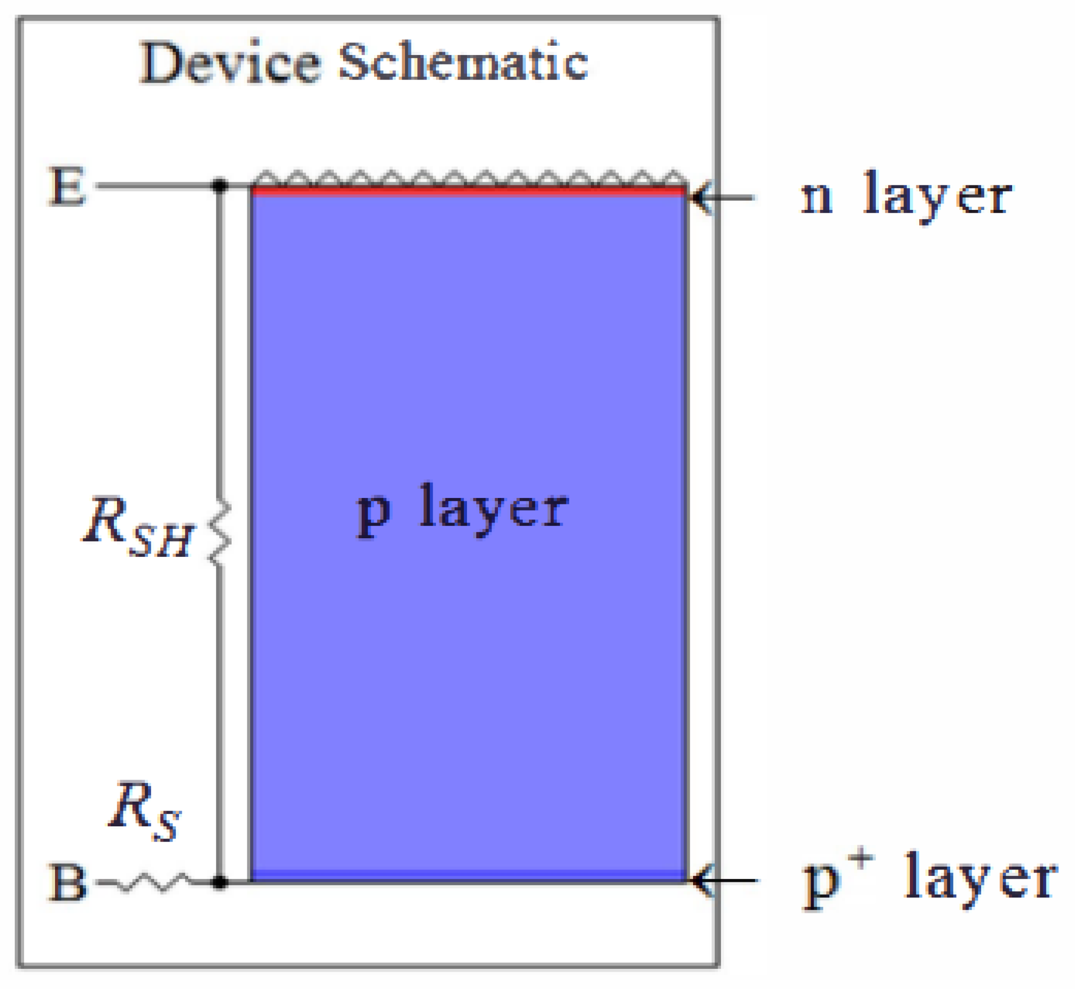
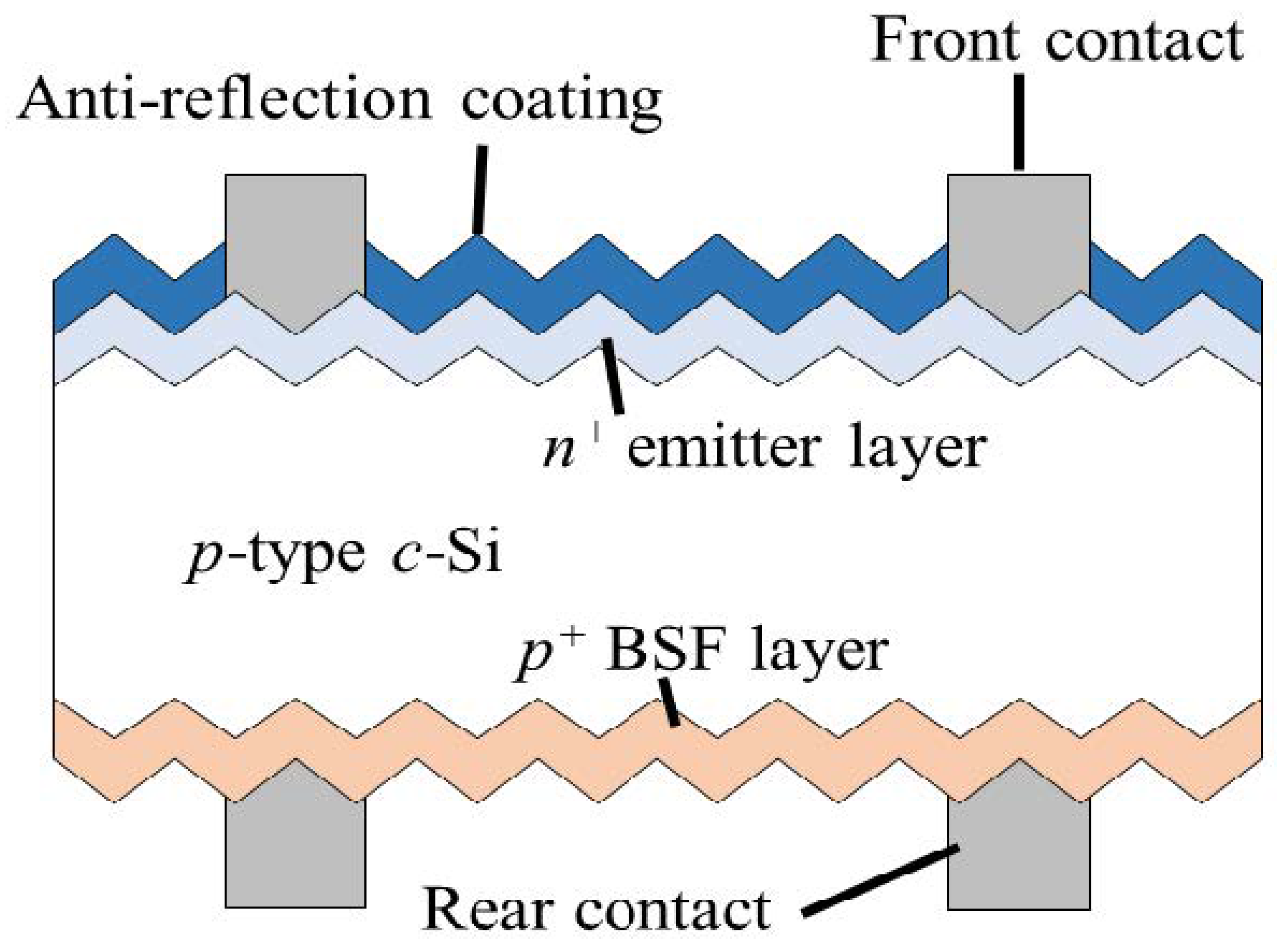
Therefore, many researchers worldwide are working on developing a numerical model for solar cell device simulation. An overview of different numerical simulation software’s present in the literature for carrying out the silicon solar cell device simulation is presented in Table 1. PC1D [3,4,5], T C A D (Silvaco and Sentaurus) [6,7], A F O R S H E T [8,9], Gridller [10], SolarEye [11,12,13] Quokka [14] are some of the solar cell simulators available for modelling the solar cell. PC1D is the most widely used tool of the commercially available solar cell modeling programs developed by the University of New South Wales, Australia [3] to understand the physics of the device. For the solar cell developers, PC1D is open-source, extremely informative, allows to model and realize all crucial factors constituting a solar cell. PC1D can simulate solar cells based on silicon, germanium, G a A s , a S i , I n P , A l G a A s , etc., PC1D allows the variation in parameters such as bulk doping levels, temperature, doping concentration variation in the emitter, back surface field (BSF), and carrier lifetime, etc., to visualize the performance of the solar cell. PC1D provides the solar cell device performance such as current-voltage (I-V) curve, open circuit voltage ( V o c ) , short circuit density ( J s c ) , external and internal quantum efficiencies, etc., in a graphical format. These results help in analyzing as well as for planning the fabrication of real solar cell devices.
Several researchers have used PC1D to simulate different types of solar cells before working on the experimental fabrication to substantiate the feasibility of their research work. n + n p + silicon solar cell was simulated by Mihailetchi et al., using PC1D software [32]. To improve the device’s performance, they varied the surface recombination velocity (SRV), the wafer’s resistivity, and the lifetime of the absorber layer to demonstrate an efficiency of 17.5%. Sepeai et.al simulated a bifacial solar cell [7,33], and Meenakhshi et.al simulated multi-junction solar cells [34] by PC1D. Huang et al., used the PC1D simulation to analyze the recombination loss mechanism [35]. Kim et al. studied the doping profile effect on the selective emitter solar cells by PC1D [36]. Choi et al., used the PC1D simulation to analyze the impact of emitter sheet resistance on the device performance [37]. Sopian et al., in their work critically review the different technologies used for simulating crystalline silicon solar cell and highlights the significance of the PC1D simulation tool [38]. A modified PC1D simulation model was also developed by Hang et al., with an improved user interface and a diversified collection of devices to be considered for simulation [39].
Hashmi et al. [40] simulated p-type Si solar cell using PC1D and studied the impact of n + and p + doping concentration, surface texturing and anti-reflection coating. They reported that the textured surface reduces the reflection and increases the solar cell efficiency by 2%. It was also reported that an optimum doping concentration for n + and p + can be 1 × 10 17 cm 3 and 1 × 10 18 cm 3 respectively. Similarly, the refractive index of 2.02 with 74 nm thick was considered ideal for the anti-reflection layer. However, Hashmi et al. did not consider the device parameters that are being used in the industry. In this paper, silicon solar cell devices with n + p p + structure have been simulated using PC1D with real physical device configurations for the optimization of silicon solar cells. In this work, the outcome of vital parameters such as solar cell absorber thickness, wafer resistivity (doping concentration), n + (emitter) thickness, p + BSF thickness, etc., were studied. The results revealed the significance of analyzing and obtaining the ideal value of each variable to obtain the maximum conversion efficiency. This present study explores the effects of wafer thickness, doping concentration, bulk resistivity, lifetime, and doping levels of the emitter and BSF, along with the front and back surface recombination velocity to analyze the impact on the performance of solar cell efficiency. Finally, the optimal values for different design considerations of Si solar cell fabrication are identified.

2. Simulation of c S i Solar Cell Using PC1D

Figure 2 shows a more detailed silicon solar cell model considered in the proposed study. Accurate solar cell modeling is required to study each layer’s physical and electrical parameters involving high conversion efficiency. PC1D simulation software is used to study the impact of the solar cell parameters on each layer to achieve high efficiency. This study utilized the actual device configuration for simulating and optimizing the n + p p + solar cell by PC1D simulation. Using numerical modeling tools such as PC1D to optimize the emitter configurations is that using these simulation tools reduces the cost, time, and efforts required to analyze the impact of the change in the design of the solar cells.
In PC1D simulation tool carries out crystalline Si ( c S 1 ) solar cell device simulation using the following numerical semiconductor equations for quasi-one-dimensional transport of electrons and holes in a solar cell. The following Equations (1)–(7) have been used as the base for creating a model of a silicon cell to optimize other process parameters.
J n = μ n · n · E F n
J p = μ p · p · E F p
J n and J p are the current densities of the electrons and holes in a semiconductor device, where n and p are the electron and hole density, μ n and μ p is the mobility of the electron and holes, and E F n and E F p are the diffusion coefficients commonly representing the difference in electron and hole quasi-Fermi energies E F n and E F p .
n t = · J n q + G L U n
p t = · J p q + G L U p
Δ 2 ϕ = q ϵ n p + N a c c N d o n +
Equations (3) and (4) are derived from the law of conservation of charge or the continuity equation. where G L and U n are generation rate and recombination rate. Equation (5) represents the Poisson’s equation for solving the electrostatic field problems. where N a c c and N d o n + are acceptor and donor doping concentrations.
n = N C F 1 / 2 q ψ + V n q ϕ n , i + ln n i , 0 / N C k B T
p = N V F 1 / 2 q ψ + V p q ϕ p , i + ln n i , 0 / N V k B T
PC1D performs silicon solar cell modeling by solving the three basic equations with the finite element approach. It is used to optimize many other process parameters to identify the most optimal configuration required for fabricating the silicon solar cell at an increased accuracy. The proposed study is based on improving the solar cell efficiency by determining the optimized parameters of different process parameters explained below.
η = P max I in = J mpp V mpp I in = J SC V OC F F I in
In order to evaluate the Si solar cells conversion efficiency, the ration of the maximum generated power which is the product of short circuit current density, open circuit voltage and fill factor, and the incident power is calculated.
The concentration of the electrons and holes in the c S i solar cell is modified and optimized by doping. The doping concentration and the type of doping (shallow or deep) influence the semiconductor material’s electrical conductivity, making the solar cell more efficient. The electrical conductivity of the c S i solar cell depends mainly on the parameters like the doping concentration and the mobility of the electrons and holes in the solar cell’s semiconductor region. Figure 3 illustrates the different dopant concentration levels of the c S i solar cells, and in this paper, we critically test the heavy doping region with varying sheet resistance. A detailed overview of the assumptions considered and the simulation’s experimental procedure is highlighted in the following section.
The process parameters such as wafer thickness, doping concentration of the emitter layer and BSF layer, wafer resistivity, minority carrier lifetime ( τ e f f ) front surface recombination velocity (FSRV), and back surface recombination velocity (BSRV) were investigated. During the actual solar cell fabrication, the optimized process parameters concerning doping concentration, sheet resistance ( R s h e e t ) , and junction depth are controlled by the temperature, time, gas flow ratio, and flow rate of the diffusion furnace. The optimized process parameters aid in the actual fabrication of the solar cell to extensively reduce the fabrication cost with increased cell efficiency. The process parameters used for the solar cell model are shown in Table 2. Base resistance ( 0.015   Ω ) , internal conductor ( 0.3   S ) , light intensity ( 0.1   W / cm 2 ) were kept constant during simulation. A M 1.5   G spectrum was used in this modeling.

3. Results and Discussion

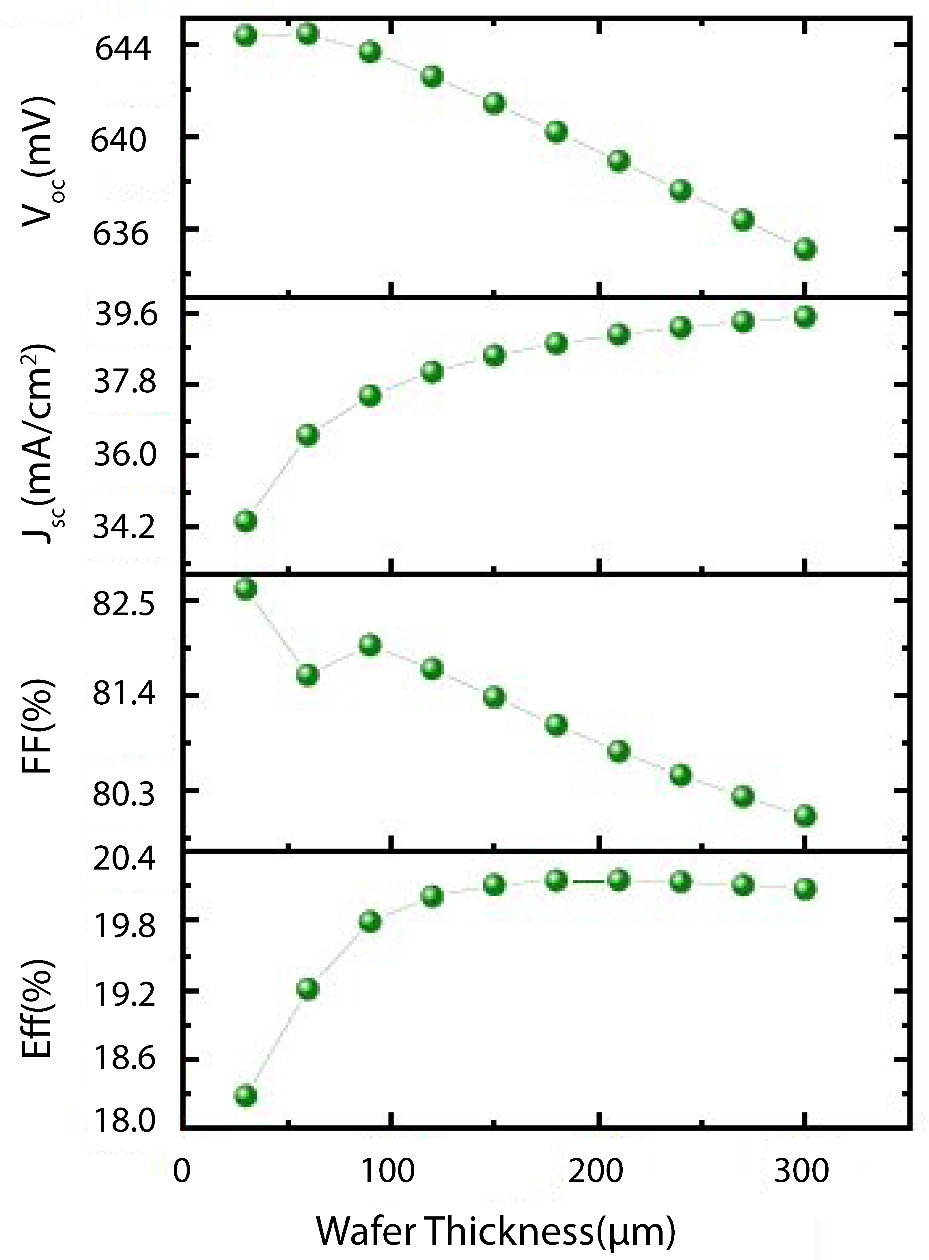
3.1. Determining the Optimal Wafer Thickness

The cost of semiconductor materials used to fabricate mono-crystalline solar cell ( c S i ) plays a significant role in estimating the photovoltaic system’s adaptability and cost. One way of reducing the material cost while maximizing the efficiency of the solar cell is by reducing the thickness of the crystalline silicon c S i wafer used in the fabrication process. Figure 4 represents the impact of the I-V parameters like open circuit voltage V o c , short circuit current density J s c , fill factor ( F F ) and efficiency with respect to the c S i wafer thickness. It is evident from the analysis that the J s c increases with an increase in wafer thickness. Also, there is no significant drop in V o c until the wafer thickness of 180 μ m is reached. Alongside, the FF reduces with an increase in wafer thickness. The maximum efficiency of the solar cell can be obtained when using a 120 μ m thick wafer, whereas the physical constraints in handling the solar cell with less than 100 μ m thick wafer have forced the PV manufacturers to consider >150 μ m thick wafers as the ideal configuration of the wafer thickness to assemble the solar cells.

3.2. Determining the Optimal Emitter Doping Concentration

The silicon solar cell’s p-n junction formation is considered one of the critical processes in solar cell device fabrication. The p-n junction is formed by diffusing a n + dopant on a p-type substrate using phosphoryl chloride. The process parameters such as temperature, time, and gas flow rate are varied to obtain an optimum doping level for the solar cell’s increased efficiency [40]. In this study, the p-type wafer with 1 Ω ·cm (doping level of 1.51 × 10 16 cm 3 ) was considered for our simulations. The effect of emitter doping concentration on the I-V parameters is shown in Figure 5. The V o c , FF and efficiency increases from 1 × 10 17 cm 3 to 1 × 10 19 cm 3 and decreases with heavy doping concentration of 1 × 10 20 cm 3 in line with observations of Cuevas et al. [41]. This decrease in solar cell performance with heavy doping concentration can be attributed to the emitter layer’s recombination process. It is evident from the observation that until the doping concentration of 1 × 10 20 cm 3 , the J s c values are constant, and after which it decreases rapidly at heavy doping.
The table inset in Figure 5 shows the variation in the sheet resistance ( R s h e e t ) and junction depth to the different doping concentrations considered for the simulation. The emitter sheet resistance ( R s h e e t ) is a crucial process control parameter in the silicon fabrication process as it has a significant impact on the cost of the system. For lightly doped emitters ( 1 × 10 17 cm 3 ), the ( R s h e e t ) lead to high series resistance and poor FF. As the doping concentration exceeds over 1 × 10 20 cm 3 , the silicon bandgap is narrowed, increasing the intrinsic carrier concentration. In case of heavily doped emitters with ( 1 × 10 21 cm 3 doping concentration, V o c ) decreases due to extreme carrier recombination at the dead layer. The prediction is that the solar cell industry will move from ( R s h e e t ) 90 to 128 ohm/sq. by 2022 [1]. Therefore the optimal value of the ( R s h e e t ) of 128 ohm/sq. is considered for our device optimization.

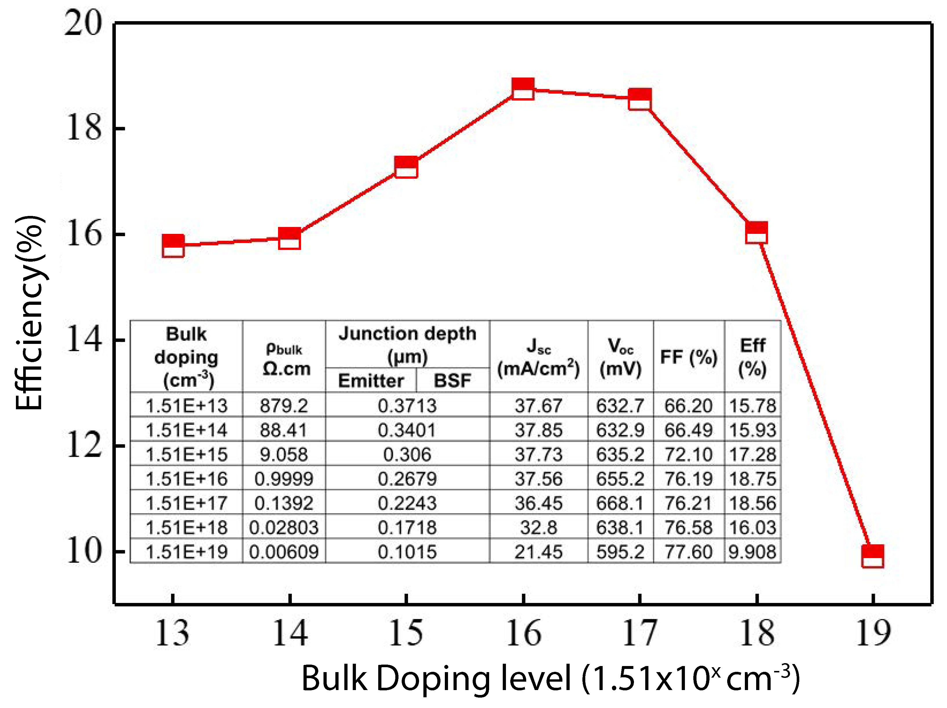
3.3. Determining the Optimal Bulk Doping Level

The wafer resistivity substantially influences the silicon solar cell’s performance because it harms the n + emitter and p + BSF doping concentration in the formation of p n junction. Based on the bulk doping concentration, the wafer resistivity can be varied. The variation in the wafer resistivity and its influence on the solar cell’s efficiency makes it an interesting aspect to consider in the fabrication of silicon solar cells. In this present work, the n + emitter and p + BSF doping concentration were kept constant at 1 × 10 20 cm 3 and 1 × 10 18 cm 3 respectively for the simulation. Bulk doping concentration was varied from 1.51 × 10 13 to 1.51 × 10 20 cm 3 and the cell efficiency was observed. Figure 6 depicts the cell efficiency as a function of bulk doping concentration. The highest solar cell efficiency of 18.75% was obtained for the doping concentration of 1.51 × 10 16 cm 3 , and then the efficiency reduces expeditiously for the bulk concentration of 1.51 × 10 19 cm 3 and more.
The higher doping concentrations reduce the minority carrier lifetime. Moreover, for the bulk doping less than 10 17 cm 3 , the radiative recombination is negligible, and hence the carrier lifetime depends on the impurity level. However, in the case of bulk doping greater than 10 18 cm 3 , the Auger recombination is dominant. The inset in Figure 6 depicts the change in emitter junction depth and BSF concerning bulk doping level. The highest junction depth of 0.37 μ m for n + emitter and p + BSF is realised at the lowest doping concentration of 1.51 × 10 13 cm 3 . Figure 6, the wafer resistivity is vital in the solar cell fabrication process and the analysis of I-V parameters. The minority carrier lifetime and the diffusion length, i.e., the average length of a generated carrier between generation and recombination, depend on the silicon wafer’s resistivity. p-type wafers with the resistivity of 0.5–2 Ω ·cm is being used in the industrial manufacturing process [42]. The good c S i wafer with a resistivity of 1 Ω ·cm value is obtained with a doping level of 1.51 × 10 16 cm 3 . From the simulated values, it is realized that the c S i wafer with a doping concentration of 10 15 to 10 16 cm 3 could lead to having 1–10 Ω ·cm of wafer resistivity of which can be used for solar cell device fabrication.

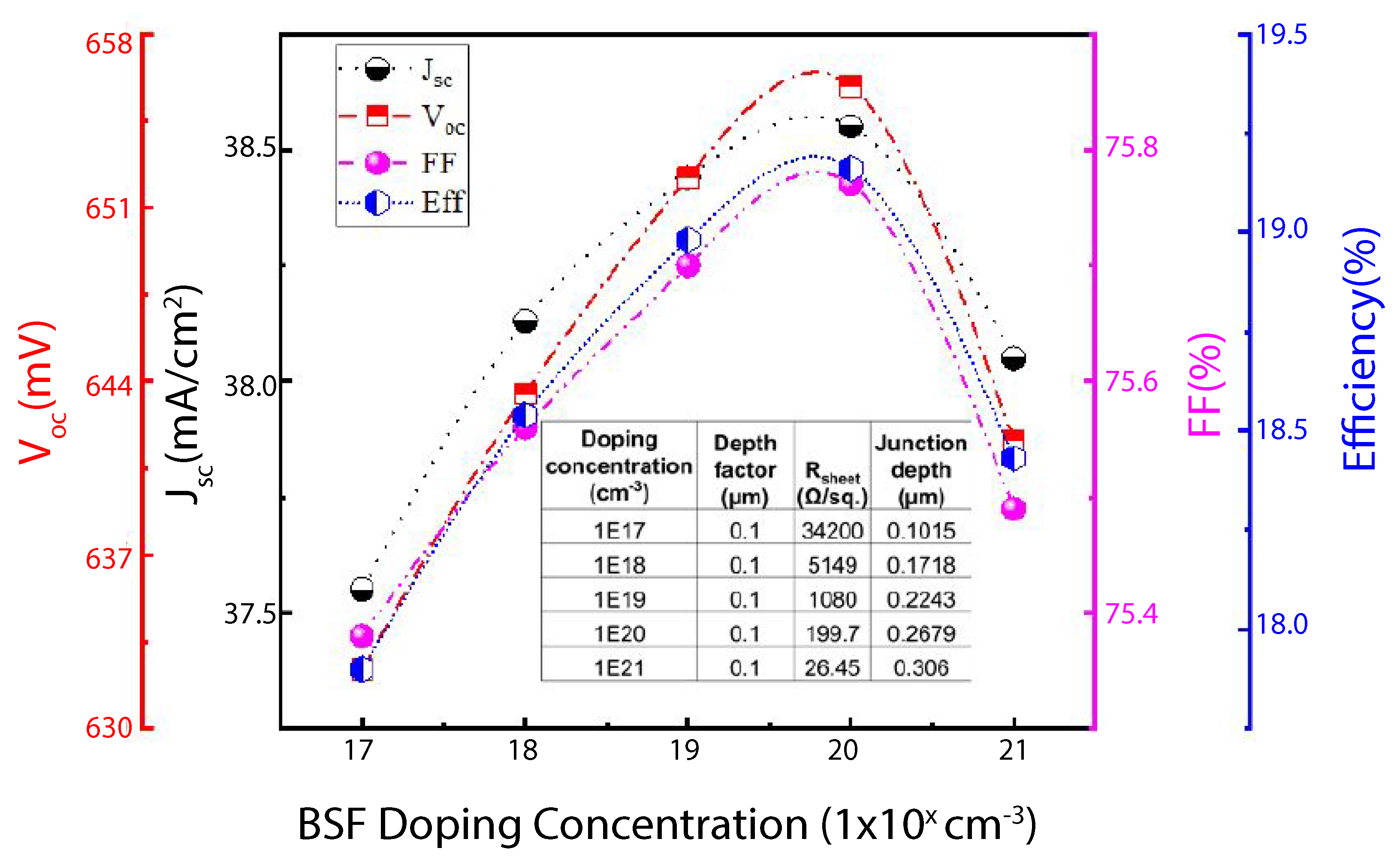
3.4. Determining the Optimal BSF Doping Level

A heavily doped layer at the rear side of the solar cell is commonly known as the back surface field [43]. The interface between the high and low doped regions (similar to a p-n junction) induces an electric field at the BSF’s junction in the solar cell. They act as a barrier for the flow of minority carriers towards the rear surface and reduces the recombination at the solar cell’s rear side. BSF doping concentration was varied on 1 Ω ·cm wafer from 10 17 to 10 20 cm 3 by fixing the n + emitter doping concentration at 1 × 10 20 cm 3 . Figure 7 indicates the I-V characteristics of the solar cell as a function of BSF doping level. It is worth mentioning that there is a rapid increase in I-V parameters with increasing doping level up to 1 × 10 20 cm 3 , and the cell performance decreases rapidly further for higher doping concentrations. The inset in Figure 7 summarizes the variation in the p + BSF junction depth and ( R s h e e t ) as a function of BSF doping concentration. Interestingly, for the p + BSF doping concentration of 10 20 and 10 21 cm 3 , practically achievable ( R s h e e t ) of 200 Ω /sq and 27 Ω /sq, respectively was realised. The increase in ( R s h e e t ) leads to an increase in contact resistance, and hence V o c of the cell decreases. The p + layer thickness is crucial in optimizing the p p + interface with low Surface recombination velocity (SRV).

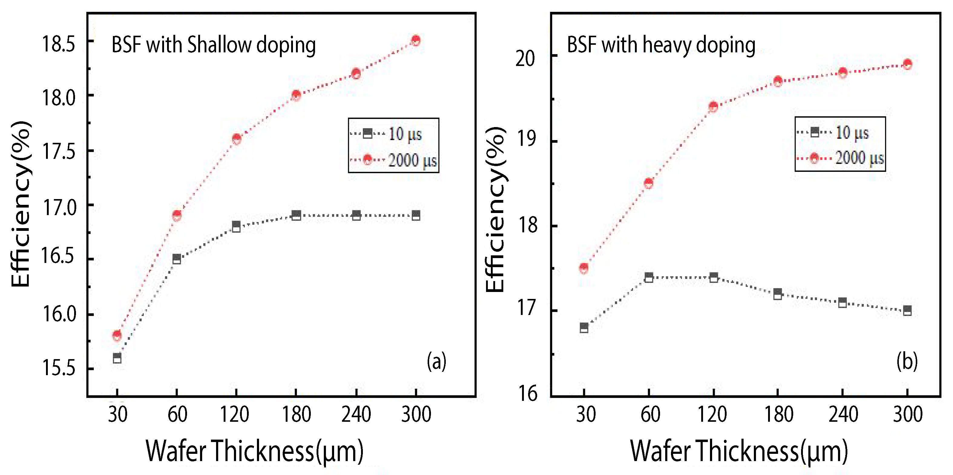
3.5. Determining the Optimal Bulk Lifetime with Shallow and Heavy Doping

Figure 8 depicts the variation in efficiency as a function of c S i wafer thickness and minority carrier lifetime of the bulk wafer (10 μ s and 2000 μ s) at shallow ( 10 17 cm 3 ) (a) and heavily doped ( 10 20 cm 3 ) p + BSF layer (b). The high lifetime wafers illustrate exceptional solar cell efficiency values for both BSF layers with shallow and heavy doping concentrations than low lifetime wafers. However, for the wafers with less than 120 μ m thick, the solar cell performance on both low and high lifetime wafers is comparable. With the increase in wafer thickness beyond 120 μ m, the solar cell efficiency variation between low and high lifetimes becomes significant.

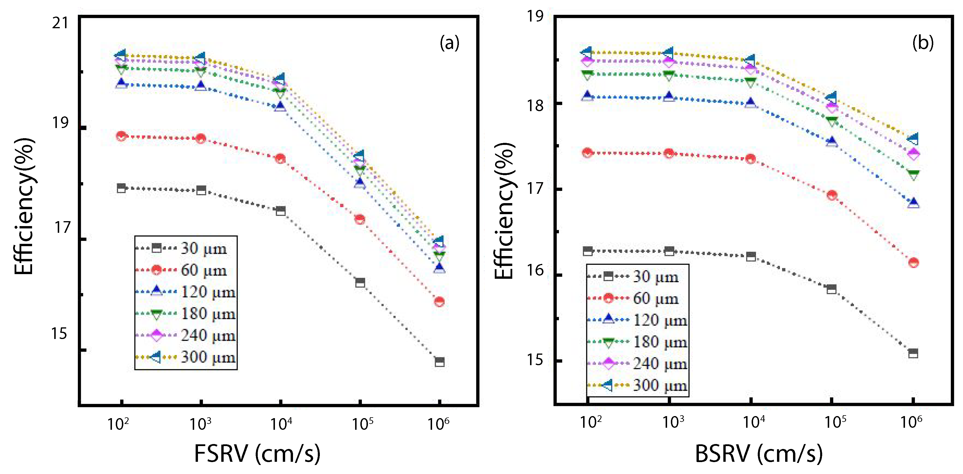
3.6. Determining the Optimal Front and Back Surface Recombination Velocity

The type of c S i wafers surface used in the silicon cell fabrication plays an important role in estimating the velocity at which the recombination of electrons and holes occurs. SRV is defined as the speed at which the charge carriers recombine at the silicon solar cell’s surface [43,44]. The solar cell efficiency variation with respect to front surface recombination velocity (FSRV) and back surface recombination velocity (BSRV) is carried out in Figure 9. By fixing the BSRV at 10 4 cm/s, the FSRV was varied from 10 2 cm/s to 10 6 cm/s. For expediency, a c S i wafer with a minority carrier lifetime of 1000 μ s was used in this simulation. For the FSRV 10 2 and 10 3 cm/s, the solar cell performance followed a similar trend for all the wafer thickness. With increase in FSRV beyond 10 2 cm/s the efficiency decreases. The simulated results show that for the high minority carrier lifetime wafers, the FSRV values between 10 3 and 10 4 cm/s can yield better efficiency. Higher the FSRV, recombination is faster and hence lower efficiency. In the case of BSRV variation, the FSRV is fixed at 10 5 cm/s. It is obvious from the simulation, with the change in BSRV, the rear surface contact impacts significantly. This effect is predominant in thin wafers. To achieve high efficiency, the BSRV should be in the range of 10 2 and 10 3 cm/s. The rear surface should be passivated with excellent passivation layers to improve the cell performance, reducing the recombination of the charge carriers at the c S i surface.

4. Conclusions

The various parameters that affect the solar cell’s device performance have been analyzed, and the optimal configuration for the silicon cell device fabrication is obtained from the study illustrated in this paper. Results indicated that the wafer resistivity with 1 Ω ·cm; 150 μ m thick silicon wafer; with n + and p + doping concentration of 1 × 10 20 cm 3 and 1 × 10 18 cm 3 respectively can yield higher efficiency of 19%. The front and back surface recombination velocity in the range of 10 2 and 10 3 cm/s is essential for obtaining the optimum efficiency. In the solar cell fabrication process, the carrier concentration of n + emitter and p + BSF concentration and wafer thickness can be adjusted with simulated values. The Photo voltaic industry focuses on the solar cell with thin wafers of <150 μ m. During the actual solar cell fabrication, the optimized process parameters concerning doping concentration, ( R s h e e t ) , and junction depth are controlled by the temperature, time, gas flow ratio, and flow rate of the diffusion furnace. Simulating these parameters in advance to determine the optimal process parameters extensively reduces the cost of fabrication. Future works will use the optimized process parameters and fabricate the actual solar cell device and compare the experimental results with the simulated results.

Author Contributions

Conceptualisation: M.S. (Maruthamuthu Subramanian), R.M.; data curation: M.S. (Maruthamuthu Subramanian), R.M., S.A., M.S. (Mohd. Shkir); formal analysis: M.S. (Mehdi Seyedmahmoudian), J.C., A.S., G.S.T.; investigation: S.A., M.S. (Mohd. Shkir), M.S. (Mehdi Seyedmahmoudian), J.C., A.S.; methodology: M.S. (Maruthamuthu Subramanian), R.M., G.S.T.; resources: S.A., M.S. (Mohd. Shkir); software: R.M., G.S.T.; writing—original draft: M.S. (Maruthamuthu Subramanian), R.M., G.S.T.; writing—review and editing: G.S.T., M.S. (Mehdi Seyedmahmoudian), J.C., A.S. All authors have read and agreed to the published version of the manuscript.

Funding

Deanship of Scientific Research at King Khalid University, Abha, Saudi Arabia for funding this work through the Research Groups Program under Grant No. RGP.1-397-42.

Institutional Review Board Statement

Not Applicable.

Informed Consent Statement

Not Applicable.

Acknowledgments

The authors would like to express their gratitude to the Deanship of Scientific Research at King Khalid University, Abha, Saudi Arabia for funding this work through the Research Groups Program under Grant No. RGP.1-397-42.

Conflicts of Interest

The authors declare no conflict of interest.

References

  1. Andreani, L.C.; Bozzola, A.; Kowalczewski, P.; Liscidini, M.; Redorici, L. Silicon solar cells: Toward the efficiency limits. Adv. Phys. X 2019, 4, 1548305. [Google Scholar] [CrossRef] [Green Version]
  2. Altermatt, P.P. Models for numerical device simulations of crystalline silicon solar cells—A review. J. Comput. Electron. 2011, 10, 314–330. [Google Scholar] [CrossRef]
  3. Clugston, D.A.; Basore, P.A. PC1D version 5: 32-bit solar cell modeling on personal computers. In Proceedings of the Conference Record of the Twenty Sixth IEEE Photovoltaic Specialists Conference, Anaheim, CA, USA, 29 September–3 October 1997; pp. 207–210. [Google Scholar]
  4. Basore, P.A. Numerical modeling of textured silicon solar cells using PC-1D. IEEE Trans. Electron Devices 1990, 37, 337–343. [Google Scholar] [CrossRef]
  5. Basore, P.A.; Clugston, D.A. PC1D version 4 for Windows: From analysis to design. In Proceedings of the Conference Record of the Twenty Fifth IEEE Photovoltaic Specialists Conference, Washington, DC, USA, 13–17 May 1996; pp. 377–381. [Google Scholar]
  6. Park, C.; Balaji, N.; Ahn, S.; Park, J.; Cho, E.C.; Yi, J. Effects of tunneling oxide defect density and inter-diffused carrier concentration on carrier selective contact solar cell performance: Illumination and temperature effects. Sol. Energy 2020, 211, 62–73. [Google Scholar] [CrossRef]
  7. Park, C.; Ahn, S.; Kim, B.; Song, K.; Choi, J.; Balaji, N.; Ju, M.; Lee, H.; Yi, J. An Analysis and Optimization of Selective Emitter with Etched-Back Structure of Crystalline Silicon Solar Cells Using TCAD Simulation. J. Comput. Theor. Nanosci. 2013, 10, 1772–1778. [Google Scholar] [CrossRef]
  8. Khokhar, M.Q.; Hussain, S.Q.; Pham, D.P.; Lee, S.; Park, H.; Kim, Y.; Cho, E.C.; Yi, J. Simulation of Silicon Heterojunction Solar Cells for High Efficiency with Lithium Fluoride Electron Carrier Selective Layer. Energies 2020, 13, 1635. [Google Scholar] [CrossRef] [Green Version]
  9. Park, H.; Khokhar, M.Q.; Cho, E.C.; Ju, M.; Kim, Y.; Kim, S.; Yi, J. Computer modeling of the front surface field layer on the performance of the rear-emitter silicon heterojunction solar cell with 25% efficiency. Optik 2020, 205, 164011. [Google Scholar] [CrossRef]
  10. Shanmugam, V.; Khanna, A.; Basu, P.K.; Aberle, A.G.; Mueller, T.; Wong, J. Impact of the phosphorus emitter doping profile on metal contact recombination of silicon wafer solar cells. Sol. Energy Mater. Sol. Cells 2016, 147, 171–176. [Google Scholar] [CrossRef]
  11. Padhamnath, P.; Wong, J.; Nagarajan, B.; Buatis, J.K.; Ortega, L.M.; Nandakumar, N.; Khanna, A.; Shanmugam, V.; Duttagupta, S. Metal contact recombination in monoPoly™ solar cells with screen-printed & fire-through contacts. Sol. Energy Mater. Sol. Cells 2019, 192, 109–116. [Google Scholar]
  12. Padhamnath, P.; Buatis, J.K.; Khanna, A.; Nampalli, N.; Nandakumar, N.; Shanmugam, V.; Aberle, A.G.; Duttagupta, S. Characterization of screen printed and fire-through contacts on LPCVD based passivating contacts in monoPoly™ solar cells. Sol. Energy 2020, 202, 73–79. [Google Scholar] [CrossRef]
  13. Shanmugam, V.; Mueller, T.; Aberle, A.G.; Wong, J. Determination of metal contact recombination parameters for silicon wafer solar cells by photoluminescence imaging. Sol. Energy 2015, 118, 20–27. [Google Scholar] [CrossRef]
  14. Fell, A.; Altermatt, P.P. A detailed full-cell model of a 2018 commercial PERC solar cell in Quokka3. IEEE J. Photovoltaics 2018, 8, 1443–1448. [Google Scholar] [CrossRef]
  15. TCAD Sentaurus. Synopsys Sentaurus Structure Editor User Guide; Spatial Corp.: Mountain View, CA, USA, 2013; pp. 1–834. [Google Scholar]
  16. Silvaco, Int. ATLAS User’s Manual; Silvaco Int.: Santa Clara, CA, USA, 2010; Volume 3. [Google Scholar]
  17. Obrecht, M.S. MicroTec-3.00 for Windows: Educational semiconductor process and device simulator. In Proceedings of the 1998 Second IEEE International Caracas Conference on Devices, Circuits and Systems, ICCDCS 98, On the 70th Anniversary of the MOSFET and 50th of the BJT. (Cat. No. 98TH8350). Isla de Margarita, Venezuela, 4 March 1998; pp. 42–45. [Google Scholar]
  18. Sara, B.; Baya, Z.; Zineb, B. Investigation of Cu (In, Ga) Se2 solar cell performance with non-cadmium buffer layer using TCAD-SILVACO. Mater. Sci. Pol. 2018, 36, 514–519. [Google Scholar] [CrossRef] [Green Version]
  19. Schwartz, R.J.; Lundstrom, M.S.; Nasby, R. The degradation of high-intensity BSF solar-cell fill factors due to a loss of base conductivity modulation. IEEE Trans. Electron Devices 1981, 28, 264–269. [Google Scholar] [CrossRef]
  20. Lundstrom, M.S. Numerical Analysis of Silicon Solar Cells. Ph.D. Thesis, Purdue University, West Lafayette, ID, USA, 1980. [Google Scholar]
  21. Girardini, K.J.; Jacobsen, S. Optimization Methods for Numerical Silicon Solar Cell Models. Ph.D. Thesis, University of California, Los Angeles, CA, USA, 1986. [Google Scholar]
  22. Kane, D.; Swanson, R. The effect of excitons on apparent band gap narrowing and transport in semiconductors. J. Appl. Phys. 1993, 73, 1193–1197. [Google Scholar] [CrossRef]
  23. Cheng, D.Y.; Hwang, C.G.; Dutton, R.W. PISCES-MC: A multiwindow, multimethod 2-D device simulator. IEEE Trans. Comput. Aided Des. Integr. Circuits Syst. 1988, 7, 1017–1026. [Google Scholar] [CrossRef]
  24. Gray, J.L. Adept: A general purpose numerical device simulator for modeling solar cells in one-, two-, and three-dimensions. In Proceedings of the The Conference Record of the Twenty-Second IEEE Photovoltaic Specialists Conference, Las Vegas, NV, USA, 7–11 October 1991; pp. 436–438. [Google Scholar]
  25. Liang, M.; Law, M.E. An object-oriented approach to device simulation-FLOODS. IEEE Trans. Comput. Aided Des. Integr. Circuits Syst. 1994, 13, 1235–1240. [Google Scholar] [CrossRef]
  26. Fossum, J.; Sarkar, D.; Mathew, L.; Rao, R.; Jawarani, D.; Law, M. Back-contact solar cells in thin crystalline silicon. In Proceedings of the 2010 35th IEEE Photovoltaic Specialists Conference, Honolulu, HI, USA, 20–25 June 2010; pp. 003131–003136. [Google Scholar]
  27. Jimeno, J.; Uriarte, S.; Zamora, J.; Icaran, C. New Concepts in 2-Dimensional Solar Cell Modeling. In Proceedings of the Tenth EC Photovoltaic Solar Energy Conference, Lisbon, Portugal, 8–12 April 1991; pp. 75–78. [Google Scholar]
  28. Bank, R.E.; Rose, D.J.; Fichtner, W. Numerical methods for semiconductor device simulation. SIAM J. Sci. Stat. Comput. 1983, 4, 416–435. [Google Scholar] [CrossRef]
  29. Muller, S.; Kells, K.; Fichtner, W. Automatic rectangle-based adaptive mesh generation without obtuse angles. IEEE Trans. Comput. Aided Des. Integr. Circuits Syst. 1992, 11, 855–863. [Google Scholar] [CrossRef]
  30. Glunz, S.; Schumacher, J.; Warta, W.; Knobloch, J.; Wettling, W. Solar cells with mesh-structured emitter. Prog. Photovolt. Res. Appl. 1996, 4, 415–424. [Google Scholar] [CrossRef]
  31. Granek, F.; Hermle, M.; Huljić, D.M.; Schultz-Wittmann, O.; Glunz, S.W. Enhanced lateral current transport via the front N+ diffused layer of n-type high-efficiency back-junction back-contact silicon solar cells. Prog. Photovolt. Res. Appl. 2009, 17, 47–56. [Google Scholar] [CrossRef]
  32. Mihailetchi, V.; Geerligs, L.; Komatsu, Y.; Buck, T.; Röver, I.; Wambach, K.; Knopf, C.; Kopecek, R. High efficiency industrial screen printed n-type mc-si solar cells with front boron emitter. In Proceedings of the 22th European Photovoltaic Solar Energy Conference, Milan, Italy, 3–7 September 2007; pp. 1581–1585. [Google Scholar]
  33. Sepeai, S.; Zaidi, S.H.; Desa, M.; Sulaiman, M.; Ludin, N.; Ibrahim, M.A.; Sopian, K. Design optimization of bifacial solar cell by PC1D simulation. Parameters 2013, 3, 5. [Google Scholar]
  34. Meenakshi, S.; Baskar, S. Design of multi-junction solar cells using PC1D. In Proceedings of the 2013 International Conference on Energy Efficient Technologies for Sustainability, Nagercoil, India, 10–12 April 2013; pp. 443–449. [Google Scholar]
  35. Huang, H.; Lv, J.; Bao, Y.; Xuan, R.; Sun, S.; Sneck, S.; Li, S.; Modanese, C.; Savin, H.; Wang, A.; et al. 20.8% industrial PERC solar cell: ALD Al2O3 rear surface passivation, efficiency loss mechanisms analysis and roadmap to 24%. Sol. Energy Mater. Sol. Cells 2017, 161, 14–30. [Google Scholar] [CrossRef]
  36. Li, X.; Lee, K.R.; Wang, A. Chemical bond structure of metal-incorporated carbon system. J. Comput. Theor. Nanosci. 2013, 10, 1688–1692. [Google Scholar] [CrossRef]
  37. Choi, J.; Song, K.; Balaji, N.; Park, C.; Ju, M.; Ahn, S.; Lee, H.; Yi, J. A Simulation Study on the Shallow Emitter Sheet Resistance for Selective Emitter Crystalline Silicon Solar Cell with Screen Printed Etched Back Process. J. Comput. Theor. Nanosci. 2013, 10, 1767–1771. [Google Scholar] [CrossRef]
  38. Sopian, K.; Cheow, S.; Zaidi, S. An overview of crystalline silicon solar cell technology: Past, present, and future. AIP Conf. Proc. 2017, 1877, 020004. [Google Scholar]
  39. Haug, H.; Greulich, J. PC1Dmod 6.2–Improved simulation of c-Si devices with updates on device physics and user interface. Energy Procedia 2016, 92, 60–68. [Google Scholar] [CrossRef]
  40. Hashmi, G.; Akand, A.R.; Hoq, M.; Rahman, H. Study of the enhancement of the efficiency of the monocrystalline silicon solar cell by optimizing effective parameters using PC1D simulation. Silicon 2018, 10, 1653–1660. [Google Scholar] [CrossRef]
  41. Cuevas, A.; Sinton, R.A. Characterisation and diagnosis of silicon wafers and devices. In Practical Handbook of Photovoltaics; Elsevier Science: Amsterdam, The Netherlands, 2005; pp. 163–188. [Google Scholar]
  42. Baliozian, P.; Tepner, S.; Fischer, M.; Trube, J.; Herritsch, S.; Gensowski, K.; Clement, F.; Nold, S.; Preu, R. The international technology roadmap for photovoltaics and the significance of its decade-long projections. In Proceedings of the 37th European PV Solar Energy Conference and Exhibition, Lisbon, Portugal, 7–11 September 2020; Volume 7, p. 11. [Google Scholar]
  43. Ahmed, M.; Ahmad, S.; Subhyaljader, M. Study the role of effective parameters in enhancement of the silicon solar cell performance using pc1d simulation. J. Ovonic Res. 2020, 16, 97–106. [Google Scholar]
  44. ALIa, K.; Tariq, Z.; Khan, H.; Javed, Y.; Sultan, M.; Anmol, M.; Usman, I.A.M.; Jameel, M.; Sajjad, M.; Alia, A. Analysis of Non-Uniform Doping in Silicon Solar Cell and Optimization Using PC1D. J. Ovonic Res. 2019, 15, 215–220. [Google Scholar]
Figure 1. Schematic of the solar cell model.
Energies 14 04986 g001
Figure 2. Silicon solar cell structure used for this study.
Energies 14 04986 g002
Figure 3. Dopant concentration levels.
Energies 14 04986 g003
Figure 4. I–V characteristics as a function of wafer thickness.
Energies 14 04986 g004
Figure 5. I–V characteristics as a function of emitter doping concentration.
Energies 14 04986 g005
Figure 6. Efficiency variation with respect to bulk doping level. Inset shows the variation in the I–V parameters as function of bulk doping level.
Energies 14 04986 g006
Figure 7. I–V characteristics with respect to BSF doping level. Inset shows the variation in the I–V parameters as function of BSF doping level.
Energies 14 04986 g007
Figure 8. Efficiency variation with respect to bulk lifetime (a) BSF with shallow doping, (b) BSF with heavy doping.
Energies 14 04986 g008
Figure 9. Efficiency variation with respect to (a) FSRV and (b) BSRV.
Energies 14 04986 g009
Table 1. Overview of numerical simulation tools used for simulating Silicon solar cell devices.
S. No.SoftwareHighlightsRef.
1SENTUARUS ATLAS MICROTECSentuarus, atlas, and microtec are general-purpose device simulation tools in which specific parameters are adjusted for solar cell simulation.[15,16,17,18]
2SCAPIDSCAPID helps investigate the limits of the open-circuit voltage used to analyze conductivity modulation in concentrated cell configuration.[19,20,21]
3SEEMASolar-Cell Efficiency Estimation Methodology and Analysis (SEEMA) is one of the first process simulation tools combined with device simulation.[22]
4PISCES IIBPISCES IIB is one of the earliest simulations of floating junctions which consisted of two-dimensional cell structures.[23]
5ADEPTTwo and three dimensions solar cell simulations were the standouts, in general, used for simulating silicon solar cells, which are made of materials other than crystalline silicon.[24]
6AFORSHETAFORSHET is mainly used for heterostructure solar cells like crystalline wafers with amorphous layers.[8,9]
7FLOODS SIMUL DESSISFLOODS are object-oriented silicon solar cell simulation tool, uses the Monte Carlo simulation technique for performing transient analysis. SIMUL is used to analyze Si solar cells with record efficiency levels. DESSIS was applied to emitters with a mesh structure, thin cells on transparent substrates, and recently rear-contacted cells.[2,25,26,27,28,29,30,31]
8TCADTechnology Computer-Aided Design is an electronic design automation tool that can be used to models semiconductor fabrication and semiconductor device operation.[6,7]
9Solar EyeSolar Eye is a web-based PV software for remote monitoring and management of solar photovoltaic systems. It helps in simulating fault isolation, yield maximization, and return of investment.[11,12,13]
10GridllerGridller is a MATLAB plugin used to design, simulate, analyze, learn, and improve silicon solar cell performance.[10]
11QuokkaQuokka numerically solves the 1D/2D/3D silicon solar cell devices, and it is an integrated part of the PV lighthouse software package.[14]
12PC1DThe modeling tool with finite element methodology is well suited for 1D and 2D silicon cell simulations. PC1D outperforms the other tools regarding its speed, user interface, and continual updates to the latest cell models. PC1D can simulate new device performance and for new users to develop an understanding of device physics.[3,4,5]
Table 2. Unique characteristics of each appliance used in the simulations.
CharacteristicsValue
Device area100 cm 2
Front/ rear surface texture depth 54 . 74 /3 μ m
Front/Rear surface coating S i N x 80 nm n = 2.03
Internal optical reflectanceEnabled
Thickness180 μ m
Intrinsic concentration ni @ 300 K 1 × 10 10 cm 3
n + diffusion 1 × 10 20 cm 3
p + diffusion 1 × 10 18 cm 3
Front and rear SRV10,000 cm/s
Bulk recombination100 μ s
Temperature25 °C
Publisher’s Note: MDPI stays neutral with regard to jurisdictional claims in published maps and institutional affiliations.

