1. Introduction
Based on convenience and safety, wireless power transfer (WPT) technology has been developed rapidly in the field of electric vehicles [
1,
2,
3], urban rail transit [
4], motor control [
5,
6], LED [
7], and so on. Along with the development and optimization of new devices [
8,
9], topology and coil structure [
10,
11], the performance of WPT system has greatly improved.
For WPT system, bidirectional power transfer can improve the energy utilization and increase the interaction between the power grid and electrical equipment, such as vehicle-to-grid (V2G), autonomous underwater vehicle, implantable medical devices [
12,
13,
14]. However, for the industrial applications, it is necessary to monitor the actual working state of the devices, and the information transfer needed [
15]. Reliable communication between the primary and secondary side plays a critical role in wireless transmission systems. If communication between the two sides is provided, it is easier to implement system requirements in specific applications, such as output voltage feedback control, load detection and status monitoring.
Varshney [
16] proposed a simultaneous wireless information and power transfer technology (SWIPT) for the first time, giving a trade-off method between signal capacity and energy efficiency suitable for discrete channels and Gaussian channels. Subsequently, Grover et al. [
17] proposed a circuit model that uses a coupled inductance circuit to achieve the simultaneous transmission of short-range wireless information and energy, and applied the water injection algorithm to the SWIPT system to achieve the optimal distribution of information energy power. In view of the fact that the actual hardware may not be able to demodulate information and receive energy at the same time, Clerckx et al. [
18] proposed a dynamic power allocation method, and on this basis, proposed a separate and integrated receiver. The authors in [
19,
20,
21] further studied the receiver models suitable for SWIPT, including models such as time allocation and power allocation. Power and information are transmitted in different time period, which reduces the power transmission time to a certain extent and affects the power transmission performance. In addition, in order to ensure the reliability of power transmission, the time allocated for signal transmission is relatively short, which mainly limits the signal transmission rate.
There are many ways to achieve information transmission in SWIPT system, including radio frequency (RF), dual channel mode, and shared channel mode. For Bluetooth, WiFi, NRF2401 and other RF system, the structures are simple and the transmission speed is stable. However, the reliability and stability of the system may decline in complex electromagnetic environment [
22]. The dual-channel technology employs additional information transmission coils. Due to the coupling between the coils, system analysis, and design become complicated. Shared channel technology has the advantages of high integration, stable and reliable information transmission [
23,
24,
25].
In shared channel technology, signal transmission modes can be divided into power modulation mode and carrier modulation mode [
26,
27,
28]. For the power modulation mode, the information transfer can be realized by the voltage regulation, frequency modulation or tuning. In the SWIPT system, adding a voltage regulation circuit in the main circuit, the information is modulated on the power carrier by changing the input voltage [
29]. The frequency modulation method changes inverter operating frequency that makes the system be in a resonant or non-resonant state. The information is obtained by detecting the voltage amplitude envelope [
30,
31]. The tuning method affects the current by changing the compensation parameters of the circuit, thereby achieving information transfer [
32]. These modulation methods have simple structures and principles, so they are easy to implement. However, the information transfer data are limited by the power transfer rate. Meanwhile, the power transfer quality and efficiency are affected by changing the circuit parameters and operating frequency.
For the carrier modulation mode, the baseband signal spectrum is broadened by sinusoidal carrier modulation techniques. It facilitates the transmission of signals on the channel. Literature [
33] proposed a SWIPT system, based on FD, and provided the circuit model and measurement results. Among them, the carrier frequency of power and information is 22.4 kHz and 1.67 MH, respectively. In order to reduce the influence of the information transfer frequency on the power transfer efficiency, the information transfer frequency is at least an order of magnitude higher than the power transfer frequency. In [
34], information and power are simultaneously transmitted in a single inductive link by using different carrier frequencies. Taking forward transmission as an example, the modulated high-frequency data carrier is injected into the primary side of the system. Then, the superimposed signal, composed of the power carrier and the information carrier is transmitted to the secondary side, and finally the data carrier in the superimposed signal is extracted by the demodulation module on the secondary side. This method is essentially a frequency division multiplexing (FDM) technology. Literature [
35] proposed a full-duplex communication by modulating dual carrier using quadrature phase shift keying. In [
36], frequency shift keying is used to achieve full-duplex communication through partially coupled coils. However, complex modulation and demodulation methods may limit their application space.
Although this transmission method has many advantages, there are also challenges. In full-duplex operation, the forward transmission signal and the reverse transmission signal circulate in the circuit simultaneously, and the signal is injected into the power loop, that is, there are three frequencies in the system at the same time, so there are inevitable interferences on the three coupling channels, such as the forward/reverse information transmission channel and the power transmission channel. A huge challenge to system design is posed when these complex coupling relationships are intertwined.
Taking into account the complexity of the coupling relationship in the full-duplex communication SWIPT system with a shared coupling channel, this paper proposes an analysis method based on the transmission channel, and studies the crosstalk between the power channel and the information channel, and between the forward and reverse transfer of information. A design method of full-duplex communication SWIPT system based on shared coupling channels is provided. Finally, the effectiveness of the proposed SWIPT method is verified by the experiment.
2. System Overview and Power Channel Analysis
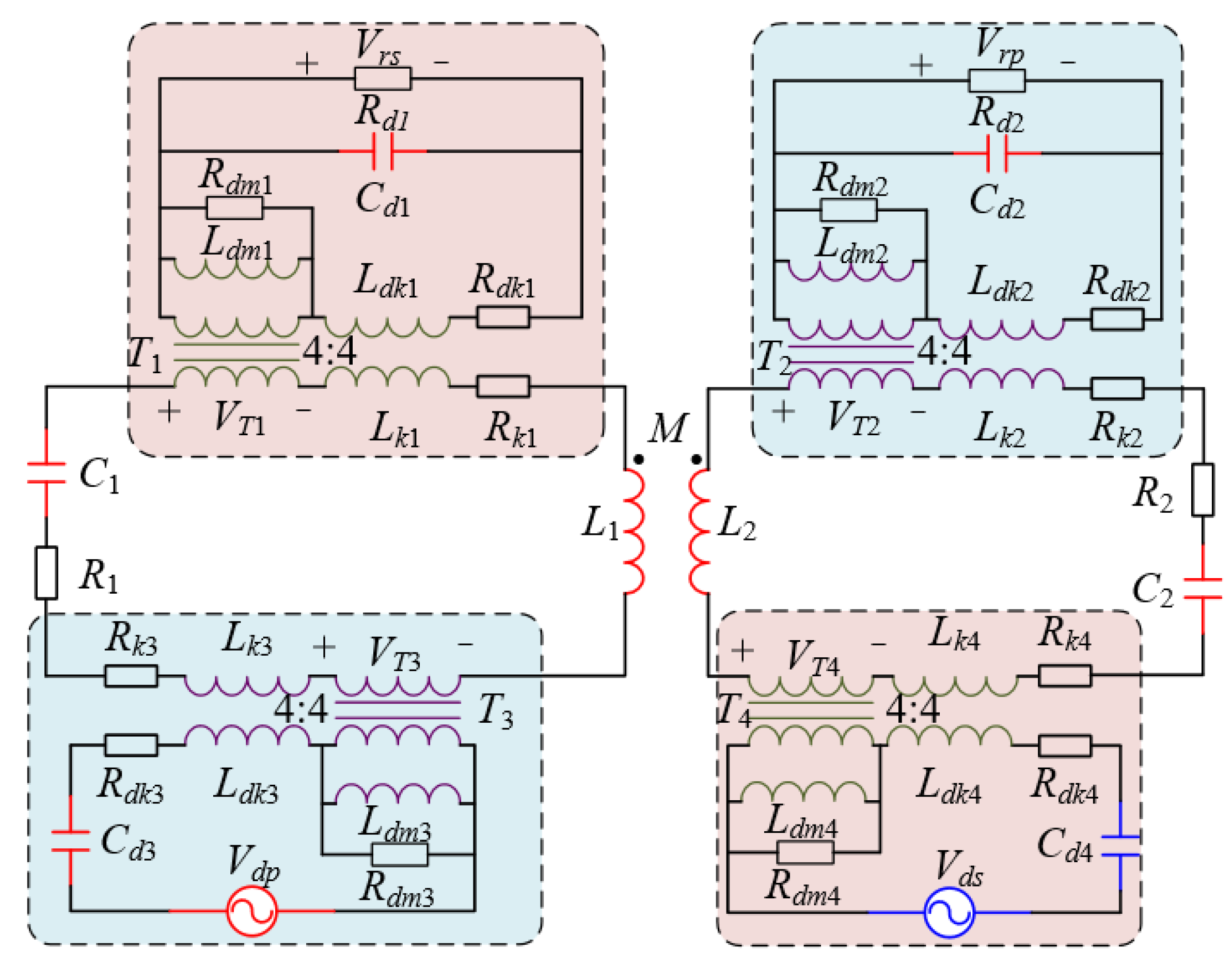
The block diagram of the proposed SWIPT system is shown in
Figure 1a. The system is divided into the primary and secondary side. Both sides are supplied by the DC power. The inductive link bridges the primary and the secondary sides. The information is injected into the bidirectional power transfer loop through the signal coupling transformer at both sides, which can achieve the full-duplex transmission of the signal.
The schematic diagram of the proposed SWIPT system is shown in
Figure 1b. The primary side and secondary side adopt the active bridges for bidirectional power transfer.
V1 and
V2 are the DC power supply in the primary and secondary side, respectively. The compensation structure of the circuit employs series compensation. Inductance and capacitance are connected in series in the circuit. As
Ip and
Is are high-frequency currents, in order to reduce the AC resistance on the coil, the inductor coil uses multiple Litz wires. Four coupled transformers (
T1~
T4) are combined to form a signal modulation section and signal receiving section to complete the transmission and reception of signals.
The combination of the transformers T1 and T4 is employed in backward information transfer. T3 and T2 are applied for forward information transfer. The forward and the backward information transfer frequency are 1.7 MHz and 1 MHz, respectively. Besides, Vdp and Vds are high frequency sources of forward information and backward information transfer, respectively. Vrp and Vrs are the voltage of forward and backward information pick-up resistances, respectively. As the injected signals frequencies are different, the transmitting circuit and the receiver circuit parameters are different and this structure can realize forward and backward information transfer dependently.
In order to achieve bidirectional power transmission, the SWIPT system adopts dual active full bridges. The power transfer size and direction is controlled by the three phase-shift, α, β, and ϕ, where α and β are half of the inter-bridge phase shift angle of the primary side and secondary sides, respectively; ϕ is the phase shift angle between the primary full-bridge arms and the secondary full-bridge arms, and it can adjust power transmission direction.
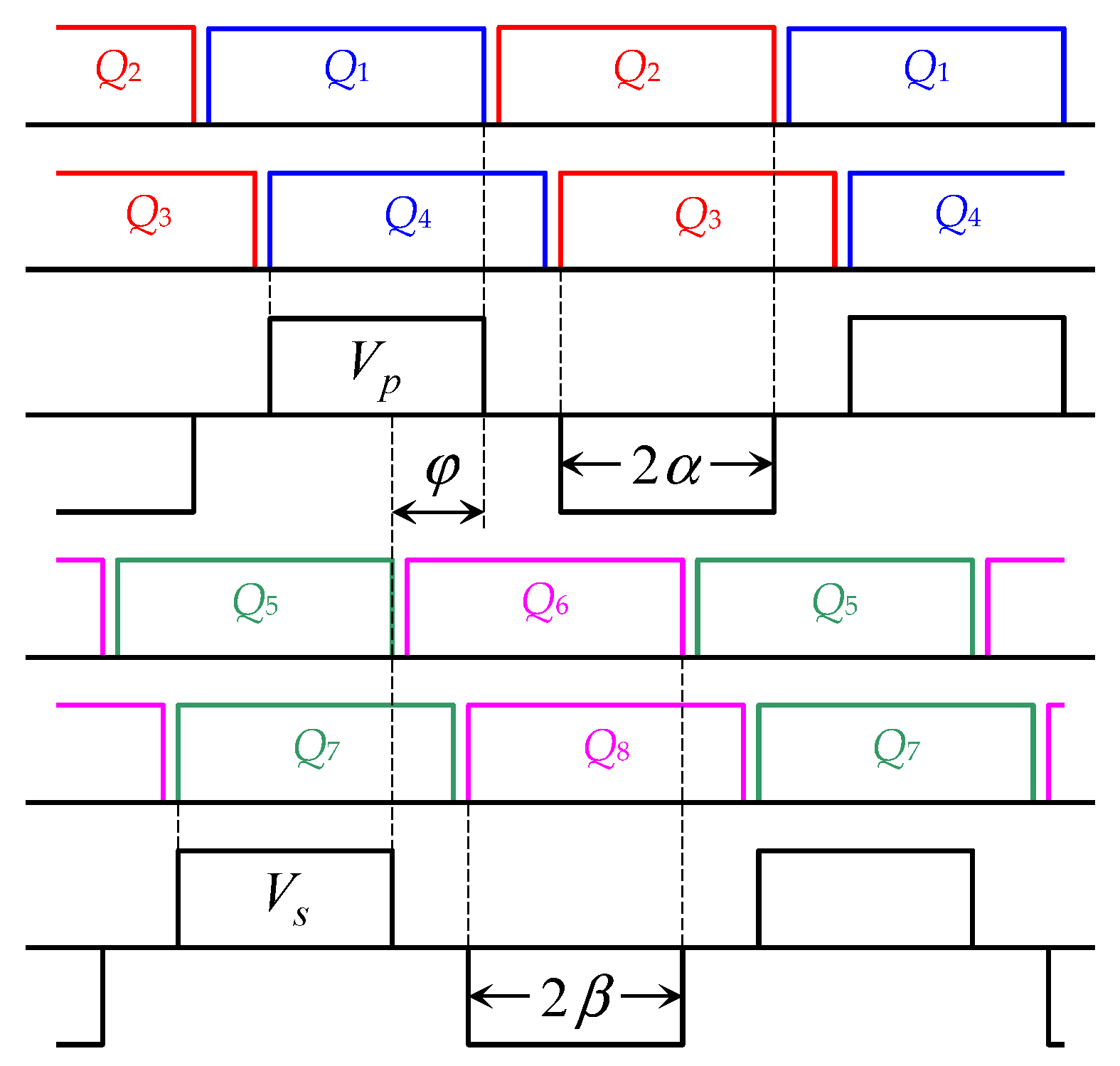
Figure 2 shows the eight switches control signals of the dual active bridges.
S1~
S4,
S5~
S8 are the primary side and secondary side control signals, respectively.
Vp and
Vs are output three-level square wave voltage signals of the primary side and secondary side.
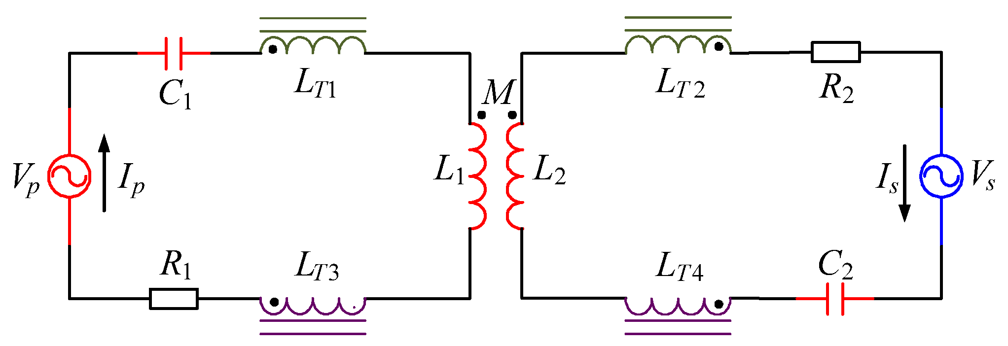
The equivalent circuit model of the proposed SWIPT system is presented in
Figure 3, where
LT1~
LT4 are the equivalent inductance of the tightly coupled transformer. During power transfer, the impedance of the tightly coupled transformer inductor
LT1~
LT4 are much smaller than the reflected impedance of information demodulation cells.
Vp and
Vs are the primary and secondary inverter output voltage. In order to simplify analysis, only the amplitude of fundamental frequency component is retained and higher harmonics are ignored. Then
Vp and
Vs are equivalent to:
Define
Vp as the reference voltage, so the expression of the
Vp and
Vs is:
where
ϕ is the phase shift angle generated between the primary side and the secondary side control signal. According to the Kirchhoff’s theorem, the circuit equation is obtained.
where
The power transfer frequency is necessary to work at the circuit resonance frequency.
C1 and
C2 compensate the inductance of the primary and secondary coils. The power resonant angular frequency
ɷp is obtained from the inductance and compensation capacitance values in the circuit.
The active power
P1 and
P2 of the primary and secondary sides are
According to the Equations (7) and (8), ignoring the resistances
Rp and
Rs, the secondary side output power
Pout is obtained.
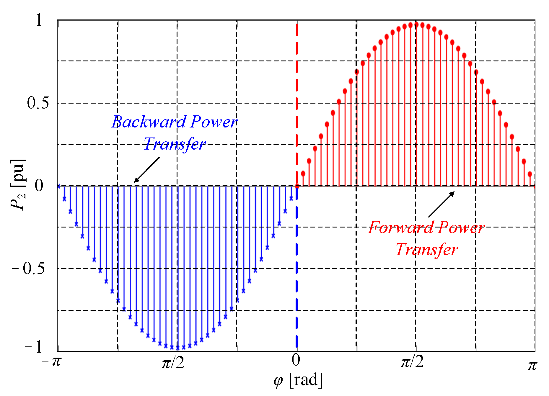
The range of α and β is [0, π]. The range of ϕ is [0, 2π]. Therefore, Equation (9) shows that the direction of the output power is determined by ϕ. The magnitude of the transmission power is affected by the phase shift angles α, β, and ϕ. The bidirectional power transfer can be realized by changing the phase shift angle ϕ.
Figure 4 shows the curve of output power with the phase shift angle
ϕ. During a period cycle, in the interval [0,
π], sin
ϕ > 0, the output power is transmitted from the primary side to the secondary side; in the interval [
π, 2
π], sin
ϕ < 0, the output power is transferred from the secondary side to the primary side. However, in order to ensure the maximum output power, the value of
ϕ is chosen between −
π/2 and
π/2. In short, the working states of the proposed SWIPT system is decided by the values of
α,
β, and
ϕ.
3. Signal Path Modeling and Analysis
In this system, information communication is implemented through magnetic induction communication technology based on the FSK control method. The carrier frequencies of forward and backward information transfer are 1.7 MHz and 1 MHz, respectively. It is obvious that the system information carrier frequencies are much larger than the power carrier frequency. According to superposition theorem, information transmission and power transmission are discussed separately. Therefore, when high frequency information is being transferred, the low frequency loop can be regarded as a short circuit to simplify the analysis of the information coupling loop. This section separately analyzes forward and backward information transmission.
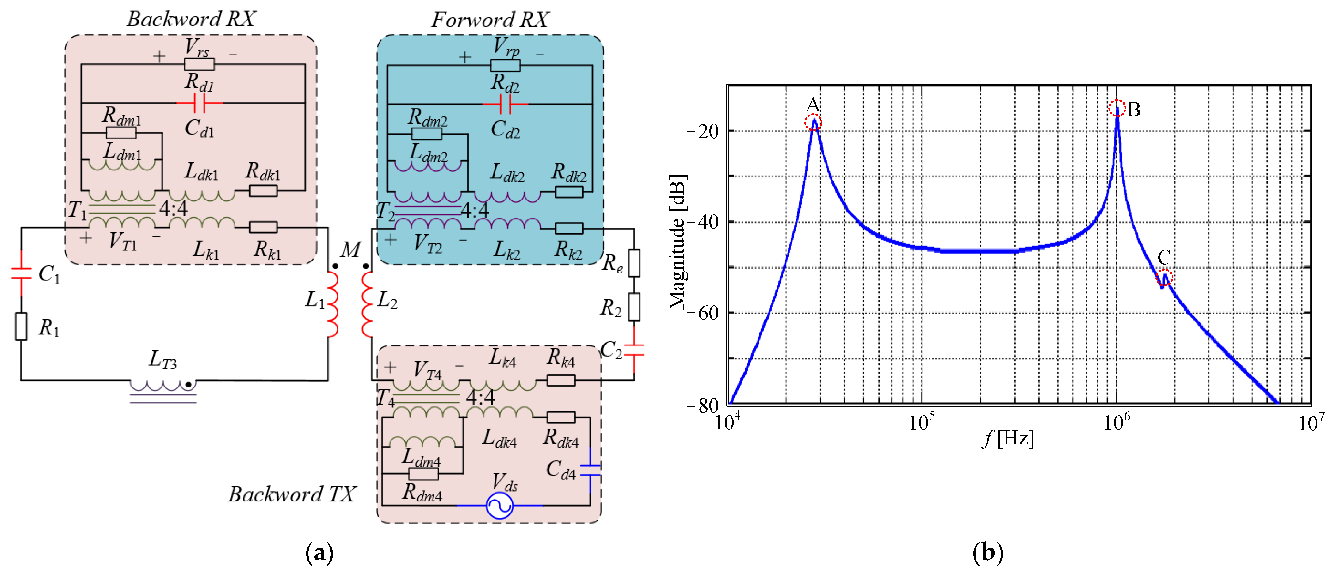
3.1. Forward Information Transfer Channel Analysis
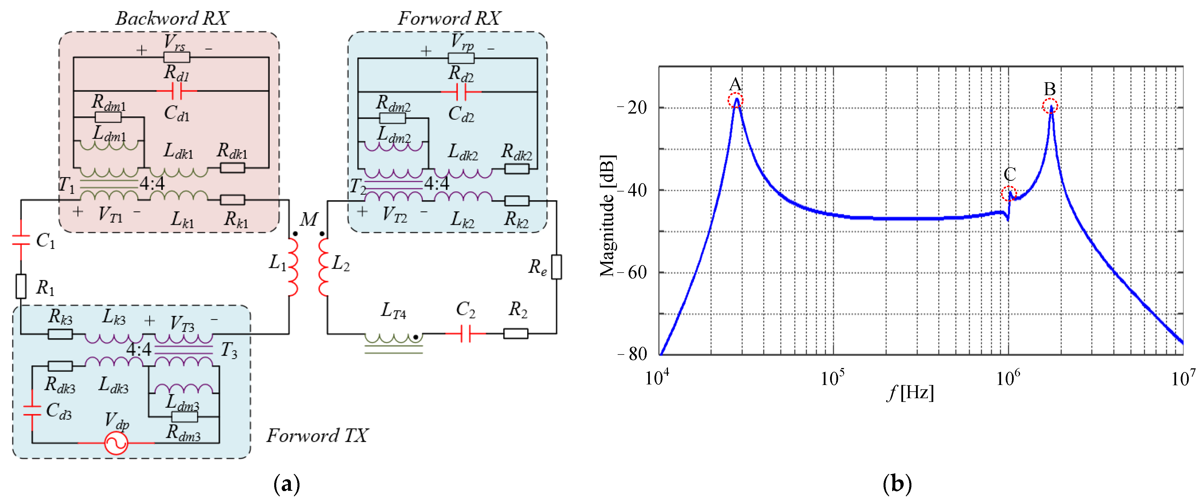
The circuit model of the forward signal transmission channel is shown in
Figure 5a. For the forward information transfer, the information is injected into the power carrier on the primary side. The information is emitted by the high-frequency source
Vdp and amplified by the
LC resonant circuit. Then, the power and the information carrier transmit through the common inductive link from the primary side to the secondary side. On the receiver side, the
LC circuit is tuned in the forward information transfer frequency to select and amplify the high-frequency carrier signal while attenuating the strength of other carriers.
In order to enhance the forward and backward information transmission and the strength of reception, the transmitting and receiving modules are resonant at the information carrier frequency. The angular frequencies of the forward or backward information transmission are ωdp and ωds, respectively.
The equivalent circuit of the signal coupling transformer is shown in
Figure 5a, where
Rmd1~
Rmd4 are the core loss resistance,
Lmd1~
Lmd4 are the mutual inductance,
Lk1~
Lk4 and
Ldk1~
Ldk4 are the leakage inductance of the four tightly coupled transformers,
Rk1~
Rk4 and
Rkd1~
Rkd4 are leakage resistance. According to
Figure 5a, the equivalent impedance of the signal receiver network is
The coupled inductance at transmitter side is ignored because its inductance is much smaller than the coil inductance. Thus, the secondary side impedance
Zs(
ɷ) is:
The impedance of the secondary side reflected in the primary side is:
The primary side impedance is equivalent to:
The gain of the information demodulation voltage at the secondary side is:
The gain of the tight coupled transform
T3 is:
So the forward information transmission gain
Gfd (
ɷ) is:
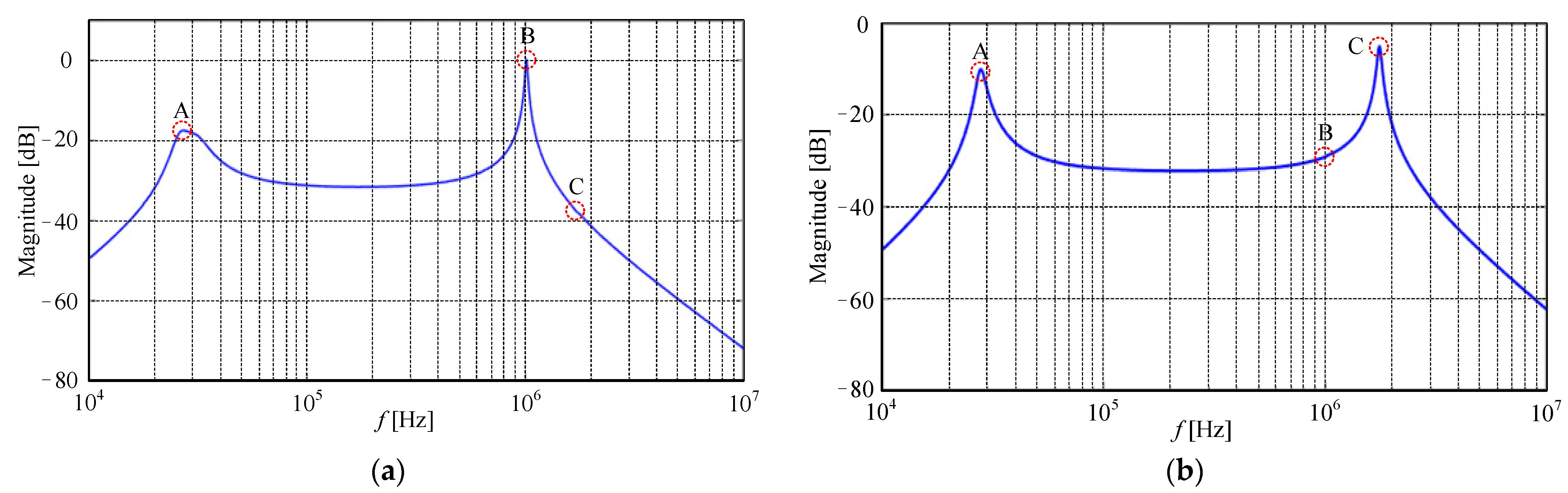
The bode plot of different carrier frequencies
Gfd (
ɷ) is shown in
Figure 5b. There exist three extreme points in this figure, where the low-frequency point A is the power carrier frequency and the higher gain frequency point B is the forward information carrier transmission frequency 1.7 MHz. Another extreme point C is the backward information transmission channel point.
3.2. Backward Information Transfer Channel Analysis
The signal backward transmission equivalent circuit is shown in
Figure 6a. Backward transmission and forward transmission are considered symmetric structures. The backward signal transmission and forward signal transmission employ similar analysis methods. When analyzing backward information transmission, the reflected impedance of demodulation circuits on both sides cannot be ignored, but the reflected impedance of the primary modulation circuit will be substituted by
LT3.
According to the equivalent circuit impedance analysis, the primary equivalent impedance
Zps is:
Zrp(
ɷ) is the reflected impedance of the primary side to the secondary side:
The secondary side equivalent impedance
Zss is:
The gain of backward information demodulation cell is:
The transfer function of the tight coupled transform
T4 is:
So the backward information transmission gain is:
The backward information transmission gain
Gbd(
ɷ) is shown in
Figure 6b. Obviously, there are also three extreme points. The lower frequency point A is the power carrier frequency. The frequencies of other two extreme points B and C are the forward and backward information transmission carrier frequencies, respectively. As shown in
Figure 6b, the backward information transmission carrier frequency is 1 MHz. The transmission gain of point B is larger than that of point C, which is advantageous to backward information transmission and demodulation.
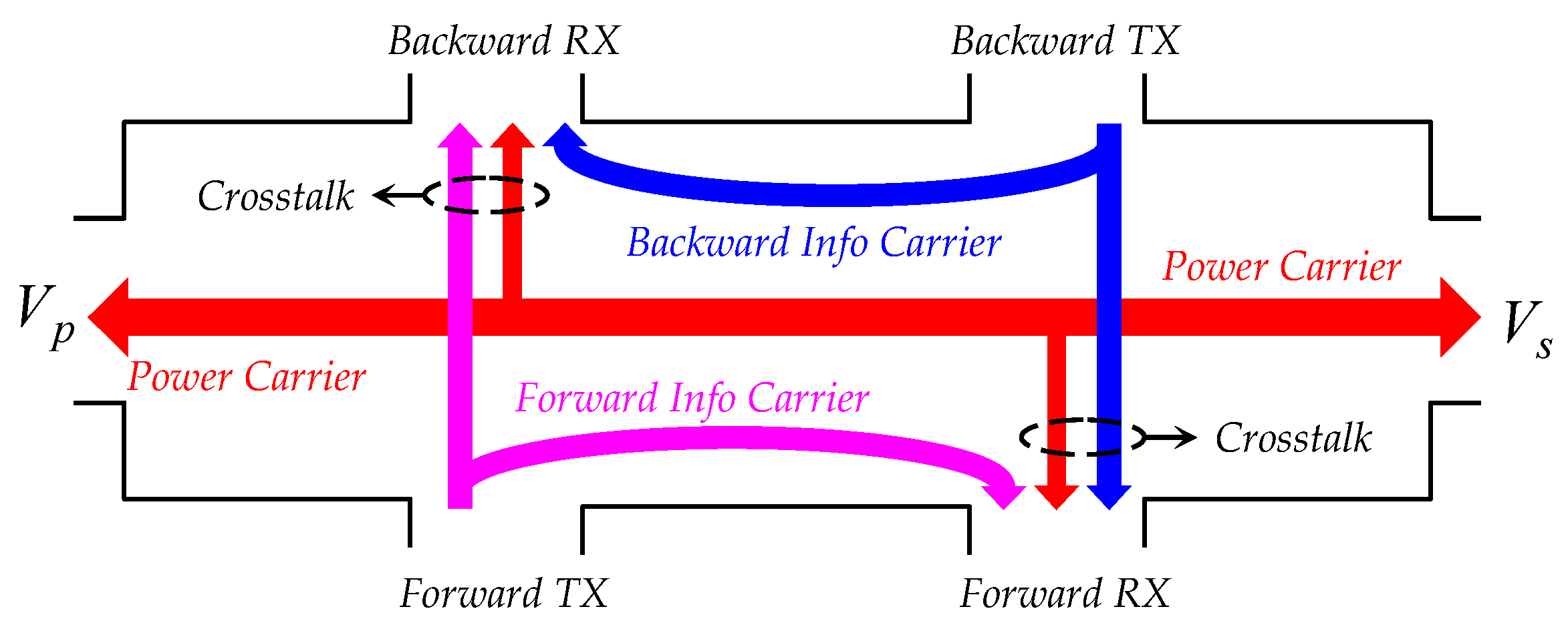
4. Crosstalk Analysis
In the proposed SWIPT system, the origin of information interference is mainly generated by the power carrier and two different frequencies information carriers. As shown in
Figure 7, the proposed SWIPT system can be equivalent to a six-port network. The power is transferred from port “
Vp” to “
Vs”. The normal forward information is delivered from “Forward TX” to “Forward RX”. The normal backward information transmission channel goes from port “Backward TX” to “Backward RX”.
Because the signal coupled coils are connected in series in the main circuit, some low-frequency voltage waveforms are also induced on the coupled coil during power transmission, so the power carrier is the main noise during signal transmission, such as “Vp” to “Backward RX” and “Vs” to “Forward RX”.
At the same time, when the information is transmitted in both directions, the signal receiving coupling coils is not only affected by the power carrier but also disturbed by another signal source, for example, “forward TX” to “Backward RX” and “Backward TX” to “Forward RX”.
To sum up, for the signal receiver cells, there are two main types of crosstalk source, one is the power carrier and the other is the high frequency signal source at the same side. Therefore, the system needs to establish two kinds of crosstalk equivalent models. Besides, it is beneficial to the design of the signal demodulation circuit by analyzing the influence of crosstalk on signal receiving port. The analysis of these two situations is as follows.
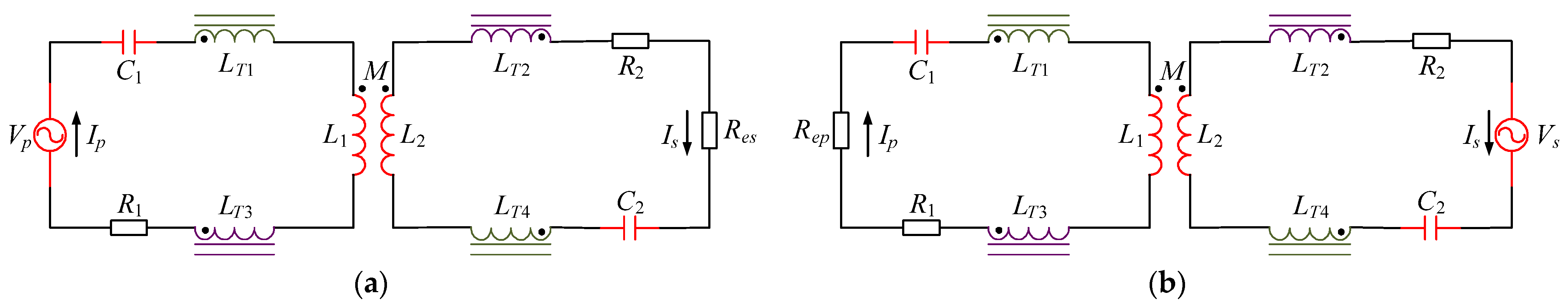
4.1. Crosstalk between Power Transfer and Information Transfer
The equivalent circuit models of crosstalk interference between power transfer and information transfer are shown in
Figure 8. When analyzing the crosstalk form power loop to information loop, the magnetic coupling interface on the signal modulation and demodulation modules are equivalent to the inductance
LT1~
LT4.
Rep and
Res are the equivalent implement of the full-bridge and DC source in the primary side and the secondary side, respectively.
As shown in the
Figure 8, the structures of circuit topologies are symmetrical. The noise interference of forward power transmission to the information loop signal transmission is analyzed. The noise transfer function
GNT1(
ω) and
GNT2(
ω) of signal receiving cells in the primary side and the secondary side are:
Define
L1 +
LT1 +
LT3 =
Lm and
L2 +
LT2 +
LT4 =
Ln, at this time, the voltages in the impedance of the primary and secondary loop coils are:
Since the coupling coefficient of the power coil is small, the reflected impedance
Zrs(
ωp) can be approximately ignored. From (24) and (26), it draws a conclusion:
Similarly, the internal resistance
R2 of the power coil on the secondary circuit is small, which has little influence on crosstalk analysis, so that it can be ignored. The voltage of power coil on the pickup side is:
According to Equations (28) and (29), the smaller the signal coupling inductance is, the lower the crosstalk interference is. Therefore, in the signal transmission process, the crosstalk interference generated from the power carrier can be weakened by reducing the coupled inductance.
4.2. Analysis of Signal-to-Noise Ratio between forward and Backward Information Transfer
In order to analyze the influence of the relationship between noise interference and information transmission, the ratio between signal power and noise is defined as the signal-to-noise ratio. Taking the forward transmission of information as an example, then we get:
The signal carrier amplitude of the secondary side information receiving end is
VR(
ɷd,
Vd), where
ɷd is the information transmission angular frequency. According to the information forward transmission channel gain
Gfd, we have:
where
Q is the quality factor of the
LC resonant circuit when the signal is accepted.
According to the transfer functions
GNT1 and
GNT2 of the power carrier to the transmitting end and the receiving end of the information forward transmission process, the power carrier amplitude of the signal receiving end is
Vr(
ωp,
Vo), where
ωp is the angular frequency of electric energy transmission. According to Formulas (24) and (25).
Incorporating the above two formulas into
SNR, the signal-to-noise ratio formula is:
Among them, Vd is the voltage of the transmission source of the information forward transmission signal, and V1 is the DC power supply of the power transmission loop. According to Formula (33), when the system coil and circuit parameters are determined, the signal-to-noise ratio of information transmission is related to the coil coupling coefficient K, the quality factor of the LC resonance circuit and the information transmission frequency. In order to improve the signal-to-noise ratio of signal transmission, the coil coupling coefficient K and quality factor Q can be improved. Therefore, when designing a signal transmission system, the system parameters should be fully and reasonably designed to reduce the system frequency transmission crosstalk and improve the signal-to-noise ratio, thereby reducing the bit error rate in the transmission, so that the signal demodulation module can successfully receive the transmitted signal and complete the information transmission.
4.3. Crosstalk between forward and Backward Information Transfer
As shown in
Figure 9, the process of bi-directional information transfer is not only influenced by crosstalk between information and power, but also interfered by the high-frequency signal source on the same side. According to the
Section 3,
Gfd(
ω) and
Gsd(
ω) are the gain of forward and backward information transfer channel, respectively. Define
Gfdc(
ω) as the gain of the channel from “Backward TX” to “Forward RX” and define
Gsdc(
ω) as the gain of the channel from “Forward TX” to “Backward RX”.
During the forward information transfer, the signal pick-up cell in the secondary side can not only receive the signal from the signal transmitter in the primary side, but also receive the signal from the signal transmitter in the secondary side.
Therefore, the crosstalk comes from the signal transmitter in the secondary side. The gain of the crosstalk
Gfdc(
ω) is:
The bode plot of crosstalk
Gfdc(
ɷ) is shown in
Figure 10a. There are only two extreme points. Point A is the power carrier, point B and point C are the information transfer gain in
ɷds and
ɷdp, respectively. However, point B is the gain of the channel from “Backward TX” to “Forward RX”, called
Gfdc(
ɷds). Comparing the gain of
Gfd(
ɷdp) and
Gfdc(
ɷds), it is clear that
Gfd(
ɷdp) is greater than
Gfdc(
ɷds). Therefore, during the process of forward information transfer, the crosstalk from “Backward TX” port would not interfere normal forward information transfer.
Similarly, during the backward information transfer, the crosstalk comes from the signal transmitter in the primary side. The gain of the crosstalk
Gsdc(
ω) is:
The bode of crosstalk
Gsdc(
ɷ) is shown in
Figure 10b. There are also only two extreme points. Point A is the power carrier, point B and point C are the information transfer gain in
ɷds and
ɷdp, respectively. Comparing the gain of
Gsd(
ɷds) and
Gsdc(
ɷdp), it is clear that
Gsd(
ɷds) is greater than
Gsdc(
ɷdp). So, during the process of forward information transfer, the crosstalk from “Forward TX” port to “Backward RX” port can be ignored.
In conclusion, normal bidirectional information transmission channels are established in primary and secondary side, but the signal receiving cells in both sides are interfered by the high-frequency source at the same side and the power carrier. According to the models of interference channels and analysis, the coupled coils inductances and self-inductance of tightly coupled transformer affect system efficiency and the gain of information transfer to a certain degree. However, the effect of these crosstalk is limited and does not affect normal information transmission, and then can be ignored.
5. Information Modulation and Demodulation
The previous section analyzes the information transfer channel of the proposed WPT system, which verifies the possibility of full-duplex communication of information. This section introduce signal modulation and demodulation model design.
The schematic in
Figure 11a is the structure of information modulation.
Vd is the DC voltage source.
QH and
QL make up high bridge inverter.
Cd is the compensation capacitor.
VT represents a modulated high-frequency voltage source, which is amplified by
LC resonance through capacitor
Cd and transformer inductor. Through transformer coupling, the high-frequency carrier signal is injected into the power loop through a high-frequency transformer. The receiver circuit in the pick-up side is coincident with the information transmission resonant point to realize the information transmission. After receiving the high-frequency carrier signal, the sampling resistor
Vr on the receiving module sends it to the demodulation circuit for signal processing. The structure of demodulation cell is shown in
Figure 11b,c.
The forward information transmission carrier frequency is set to 1.7 MHz, and the backward transmission carrier is set to 1 MHz. In order to prevent mutual interference between information carriers, the structures of forward and backward information demodulation circuits are different. Therefore, for the forward transmission carrier frequency, the secondary side information demodulation circuit uses a high pass filter (HPF) to filter out the low-frequency power wave and the 1 MHz backward information carrier. And, for backward information transmission, the primary side information processing circuit uses a band-pass filter (BPF), whose band-pass frequencies range from 900 kHz to 1.2 MHz. After passing through the envelop detection (ED) circuit, the voltage peak envelope voltage is obtained. The output waveform is obtained after the signal is sent to the amplifier and comparator circuit.
6. Experimental Verification
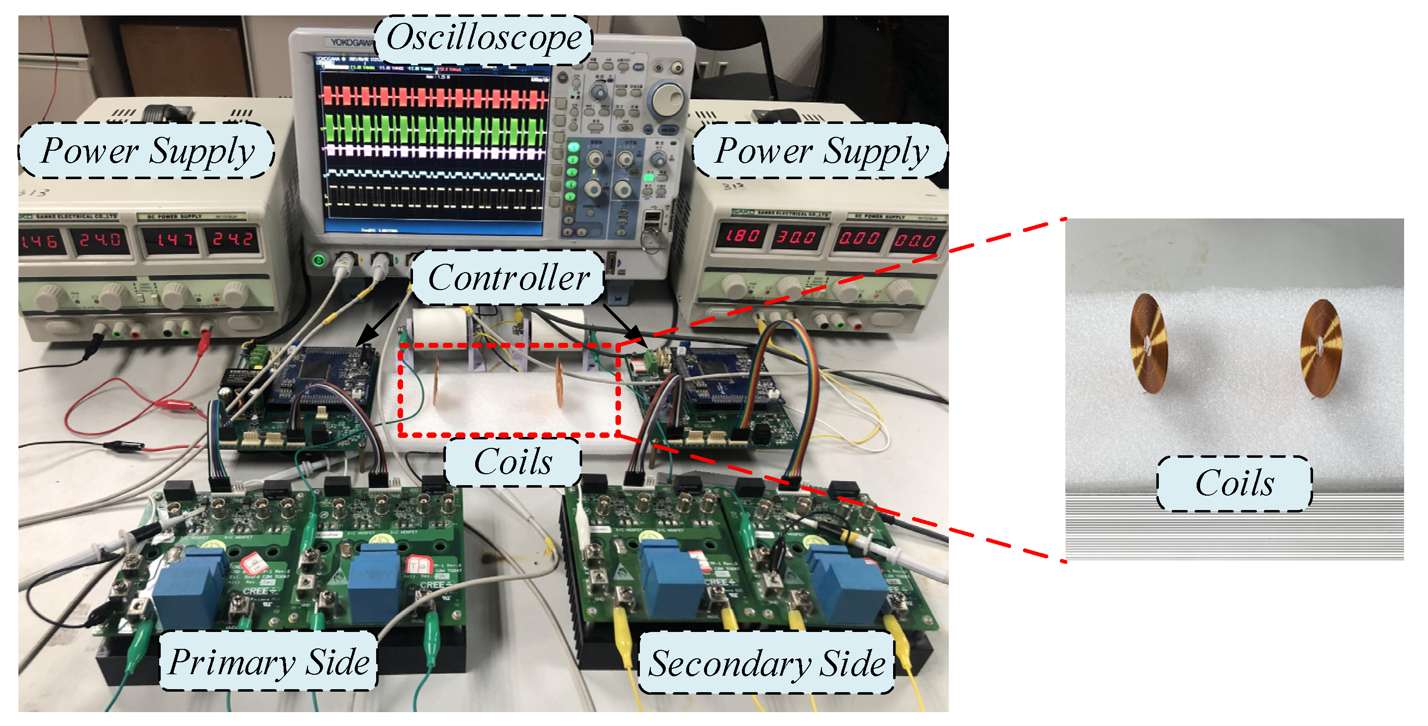
To verify the feasibility and effectiveness of the proposed topology and method, a SWIPT system with air gap of 10 cm and 60 W output power is constructed, as shown in
Figure 12, The coupling coil disc has a diameter of 8 cm. There are four signal processing boards, two of them are signal transmitting boards, and the other two are signal receiving boards. The system is designed to achieve simultaneous bidirectional transmission of power and data through a shared channel. The system parameters are shown in
Table 1.
In order to verify the feasibility of circuit principle and control mode, the current and the voltage in the primary and secondary sides are measured in the process of the experiment. At the same time, for the information transfer, the information transmission at different frequencies and the simultaneous power and information transmission are also measured in the experimental processing, respectively.
In order to verify the impact of the value of
α,
β and
ϕ in this SWIPT system, let
α = 3
π/4 and
β = 5
π/6,
ϕ is switched between −
π/2 and
π/2. When
V1 is 48 V,
V2 is 30 V, and the output power is 60 W,
Figure 13 shows the voltages and currents of the primary and secondary sides in power transfer loop.
Figure 13a displays the power transmitted from the primary side to the secondary side and
Figure 13b is the backward power transfer.
The voltages and the currents are in the same phase. Among them,
Vp and
Vs are output three-level square wave voltages of the primary side and secondary side.
Ip and
Is output the sine wave currents on the primary side and the secondary side, respectively. From
Figure 13a,b, it can be seen that the voltage and current are in phase. Therefore, both forward and reverse power transmission are normal. In addition, the operating state of the system is resonant. When
α =
π and
β =
π, there are only two-level existed in the waveform of
Vp and
Vs. If
α ≠
π and
β ≠
π, three-level waveforms appear.
As shown in
Figure 14, when the phase shift angle ϕ between the primary and secondary bridge arms changes, the direction of power transmission also changes. When the phase shift angle ϕ between the primary and secondary bridge arms changes from −π/2 to π/2, the direction of the output current I2 changes too. According to the experimental results, by changing the value of ϕ, the forward transmission of the power is changed to the reverse transmission, that is, the bidirectional transmission is completed, which verifies the previous theoretical analysis.
Both the information modulation and demodulation cells are connected in series. The full-duplex information transfer adopts frequency shift keying (FSK) control method via a shared channel with power carrier. The signal extracted by the LC frequency selection enters the high-pass filter or band-pass filter to remove the influence of the power carrier and other harmonics. After flowing through the detection circuit and the envelope circuit, the signal is sent to the comparator and amplifier circuit. Then, the demodulation module extracts the information encoding. Finally, the information-encoded square waves are obtained.
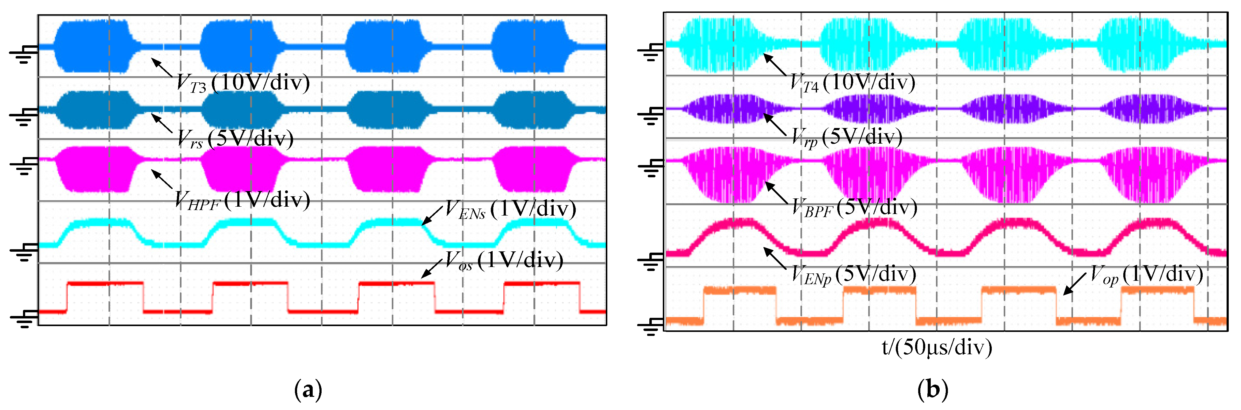
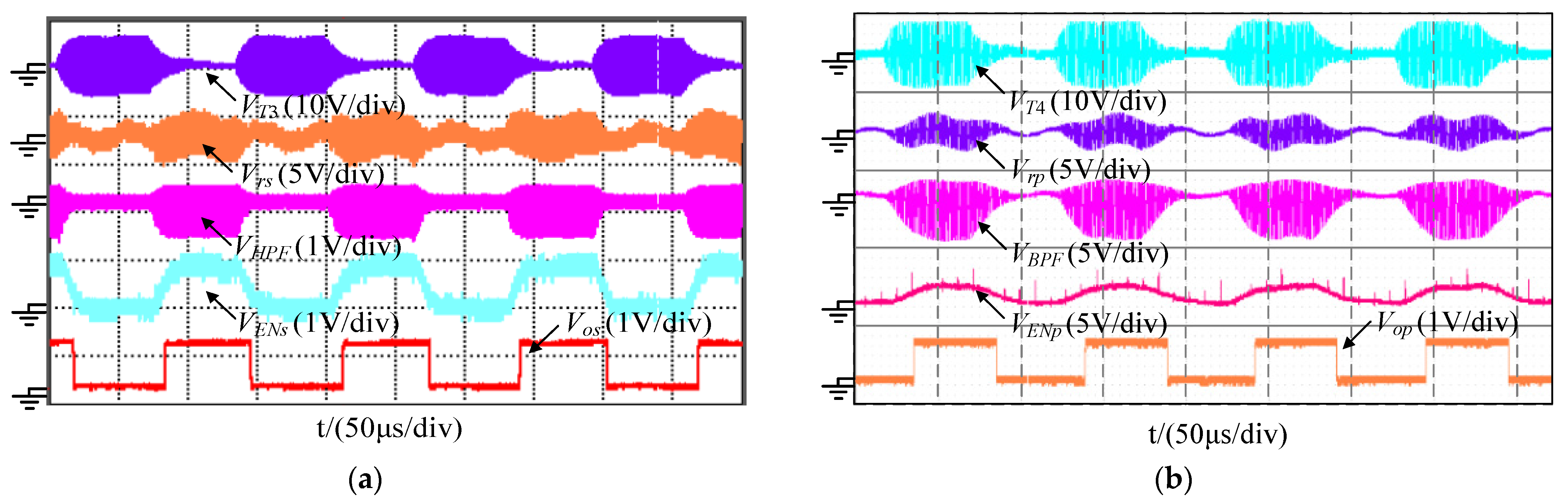
Figure 15a shows the process of only forward information transferring without power transmission and the communication rate is 20 kbps.
VT3 is the modulation signal source for the forward information transfer.
Vrs is the voltage of
Rd2.
VHPF is the output voltage of HPF. After HPF, the low-frequency power waves and other harmonic are filtered out. Then, the envelope detector will follow the peak voltage of
VHPF and its output voltage is
VENs. Finally, the forward information transfer signal will be demodulated by amplification and comparison.
Vos is the output voltage of forward information demodulation cell.
Similarly, the process of only backward information transferring without power transmission is shown in
Figure 15b.
VT4 is the modulation signal source for the backward information transfer.
Vrp is the voltage of
Rd1. Contrary to forward information transfer, the structure of demodulation cell for backward information transfer uses BPF to pick up the selected signals.
VBPF and
VENp are the output voltage of BPF and envelop detector, respectively.
Vop is the output voltage of backward information demodulation cell. According to the experimental results, the information transmission is realized correctly.
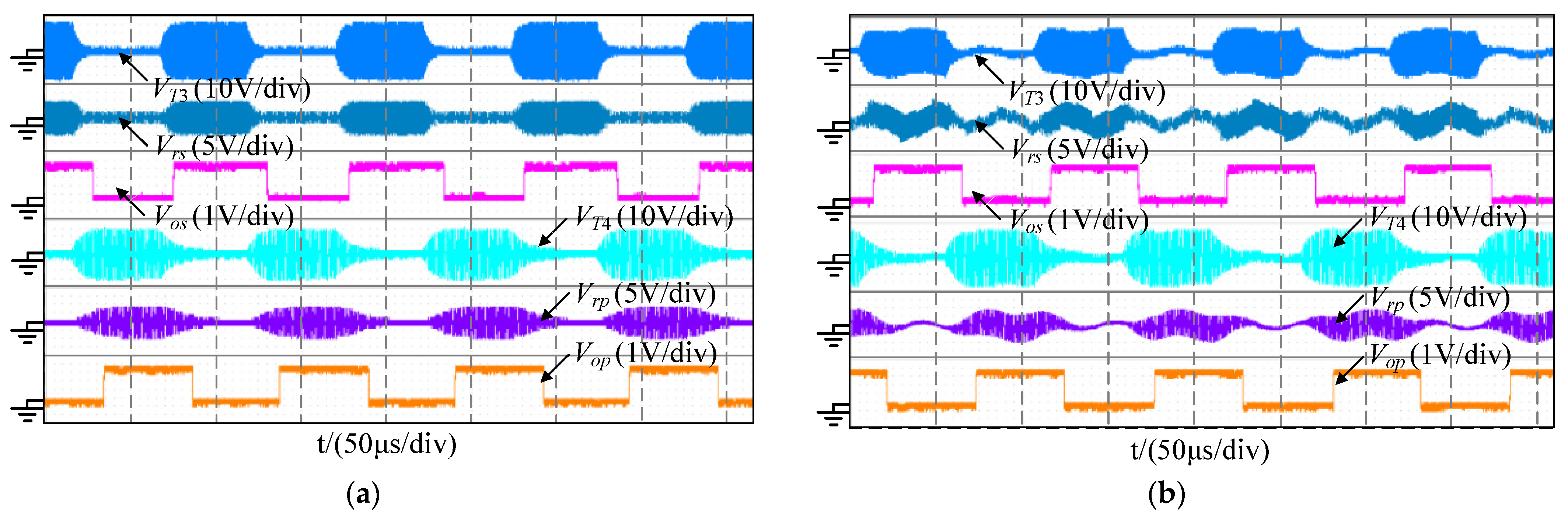
In
Figure 16a,b, the simultaneous wireless information and power transfer is implemented successfully and the communication rate is 20 kbps. The forward and backward information are injected into the power carrier through the modulation signal source in the primary and secondary sides, respectively. Then the waveforms are received at the secondary and primary sides to achieve the demodulation process. Compared with only information transfer, power transmission interferes with the information demodulation, the information can still be received correctly through information demodulation cells.
Figure 17a presents the process of simultaneous bidirectional information transmission if there is no power carrier in the circuit.
VT3 and
VT4 represent the output voltage of tight coupled transformer in primary side and secondary side, respectively.
Vrd and
Vrs represent the received high-frequency signal and the filtered information signals, which means the information transmission is completed via a shared channel.
Vop and
Vos are the information waveform obtained from the demodulation circuit in both sides.
According to these experimental results, the forward and backward information can be transmitted simultaneously and independently. Similarly,
Figure 17b verifies the simultaneous transmission of forward and backward information, the results indicate that information can still be transmitted and demodulated if there is a power carrier in the circuit.
In short, the influence of information carrier on power transmission can be ignored during power transmission; similarly, during information transmission, regardless of power transmission, information can be transferred in full duplex mode.
7. Conclusions
In this paper, a FSK-based SWIPT system with full-duplex communication via a shared channel is established. In this system, the bidirectional power and the full-duplex information transmit at the different frequencies through a shared channel.
When the system is operating, there is a mutual interference between the power transmission channel and the information transmission channel, and between the information channels in the two transmission directions, which brings great difficulties to the analysis of this type of full-duplex SWIPT system.
To solve this problem, this paper proposes an analysis method based on the transmission channel, studies the aforementioned two types of interference problems, and establishes an analysis model for power and information transmission. Experiments show that while there is a relatively complicated mutual interference relationship when the system is running, it can be simplified separately when analyzing power transfer and information transfer. In the experimental prototype, three phase shift control strategy is designed to control the level and direction of output active power. Using the most primitive information transmission method, the full duplex communication rate reaches 20 kbps, and the output active power is 60 W. The experimental results validate the proposed analysis method and model.


 ,
, 


