Article

Temperature Estimation of SiC Power Devices Using High Frequency Chirp Signals

1
School of Engineering, Newcastle University, Newcastle upon Tyne NE1 7RU, UK
2
School of Computing, Engineering and Digital Technologies, Teesside University, Middlesbrough TS1 3BX, UK
3
Department of Informatics, Technical University of Munich, Boltzmann Strasse 3, 85748 Garching by Munich, Germany
*
Author to whom correspondence should be addressed.
Energies 2021, 14(16), 4912; https://doi.org/10.3390/en14164912
Submission received: 27 June 2021 / Revised: 5 August 2021 / Accepted: 6 August 2021 / Published: 11 August 2021

Abstract

:
Silicon carbide devices have become increasingly popular in electric vehicles, predominantly due to their fast-switching speeds, which allow for the construction of smaller power converters. Temperature sensitive electrical parameters (TSEPs) can be used to determine the junction temperature, just like silicon-based power switches. This paper presents a new technique to estimate the junction temperature of a single-chip silicon carbide (SiC) metal–oxide–semiconductor field-effect transistor (MOSFET). During off-state operation, high-frequency chirp signals below the resonance frequency of the gate-source impedance are injected into the gate of a discrete SiC device. The gate-source voltage frequency response is captured and then processed using the fast Fourier transform. The data is then accumulated and displayed over the chirp frequency spectrum. Results show a linear relationship between the processed gate-source voltage and the junction temperature. The effectiveness of the proposed TSEPs is demonstrated in a laboratory scenario, where chirp signals are injected in a stand-alone biased discrete SiC module, and in an in-field scenario, where the TSEP concept is applied to a MOSFET operating in a DC/DC converter.

Graphical Abstract

1. Introduction

High-temperature, high-frequency converters are becoming increasingly important in electric vehicles (EVs) [1], also continuous developments of wide-bandgap semiconductor devices allow power converters to meet the requirements for EVs. Silicon (Si) is one of the most commonly used semiconductor materials in power electronics and associated applications, such as solar power [2]. Over the last two decades, new materials, such as gallium nitride (GaN), silicon carbide (SiC), and diamond have emerged as a future workforce for power switching devices. Currently, SiC is seen as the most attractive material for medium power levels, as it enables high voltage and current power handling capabilities. Similar to Si devices, SiC devices are vulnerable to temperature increase. Thus, knowledge of the junction temperature, T j , is required for reliable operation [3].
Monitoring T j has become sophisticated and various techniques have been proposed that can be classified into direct and indirect methods. One of the direct methods is based on the use of an infrared thermal camera (IR) and is viable for bare die type or unpackaged power devices [4]. The benefit of using IR is capturing the temperature over the full device surface area, allowing the generation of a thermal distribution map. However, IR can only be used in a laboratory setting and is also expensive; hence, it is often used for calibration or validation purposes only, rather than in-field operations [5]. Another effective and direct technique of measuring temperature is to employ embedded temperature sensors in the chip die [6]. Although this technique has not been widely applied in commercially available power devices, it is promoted by a few semiconductor manufacturers [7].
In terms of indirect methods, the use of temperature sensitive electrical parameters (TSEPs) to indirectly estimate T j has been extensively developed by establishing the knowledge of the chip temperature dependence of one or multiple electrical parameters. Numerous TSEPs have been proposed and implemented either in offline or online operation [8]. The principle to extract T j using TSEPs involves the following steps: (1) electric parameters are measured offline to determine the relationship between the electric measured parameters and the junction temperatures. This relationship is recorded and is called the baseline; (2) the baseline is stored as reference in the controller of the power converter; (3) sensors embedded around the switching device continuously capture electric parameters during operation; (4) the measured parameters from the sensors are compared with the baseline, which results in estimating T j . Mandeya and Chen et al. [9,10] list a whole range of various TSEPs for Si-based power modules, which can be divided into two groups: static and dynamic TSEPs. Static TSEPs measure the electric parameters when the switch is in its on-state or off-state. Dynamic TSEPs measure the electric parameters during the switching event.
Despite the large variety of TSEPs that have been proposed over the years for Si-based power modules, many of them are not applicable to SiC-based metal–oxide–semiconductor field-effect transistors (MOSFETs) for the following reasons: (1) voltages and currents are impacted by electromagnetic interferences caused by the fast-switching transients making measurements of dynamic TSEPs very difficult [11]; (2) oscillations in the drain-source voltage are fed back into the gate voltage loop through the Miller capacitance [12]; (3) SiC devices have considerably smaller parasitic capacitance compared to silicon-based MOSFETs due to smaller die area [13]; (4) the turn-off d V / d t of SiC MOSFETs is far less temperature dependent than Si-based MOSFETs [7].
However, attempts have been made to apply TSEPs to SiC-based MOSFETs. In [14], Stella et al., present the on-state voltage V D S as a static TSEP. To extract the value of V D S , the on-state voltage should be precisely measured, which is a challenging exercise, since V D S swings from low voltage when the device is on, to hundreds of volts when the device is off. Therefore, measuring V D S requires isolation, which increases complexity. Despite hardware complexity, V D S is less sensitive to temperature variations for SiC devices [14,15]. A variation of measuring V D S has been proposed in [16,17], where the on-state resistance R o n -state is used as static TSEP. The difference between the two is that capturing V D S requires a defined injected current through drain and source, which is difficult to implement as the load changes constantly. Two others static TSEPs have been proposed for SiC MOSFETs. In [18], the leakage current, I l e a k , was measured, and in [19] the saturation current, I s a t , was used. However, both TSEPs are only practical in offline applications.
So far, eight dynamic TSEPs have been proposed for SiC, according to the authors’ knowledge. In [15], the threshold voltage, V t h , and in [20] the quasi-threshold voltage, V t h ,   q u a s i , show low sensitivity to temperature variations, and both TSEPs are highly susceptible to noise because both values can only be measured at one specific time; therefore, they suffer from noise problems. The drain current slope, d i D S / d t , also exhibits noise issues [7] and complex behavior in SiC [21]. The same challenges are observed when measuring rising and falling times, i.e., t r , t d o n , t d o f f , and t f , all of which have been proposed as TSEPs for SiC devices [15,18,22]. In [16], the peak gate current, I p e a k , was used to determine the internal gate resistance, R G ( i n t ) , which is temperature dependent. R G ( i n t ) represents the resistance of the polysilicon gate and metal contact in a MOSFET device and consequently cannot be directly measured using terminal connections. For this reason, this TSEP is dynamic as it captures one point during the switching process.
According to the literature so far, dynamic TSEPs are unsuitable for SiC MOSFETs, mainly due to noise issues caused by significant switching transients. Static TSEPs measuring V D S or R o n -state suffer from the need of isolation circuitries, and because I l e a k and I s a t are not applicable for online operation.
Recent research works considered injecting probe signals into power devices in order to extract TSEPs from the measurements. This is due to the fact that at resonance R G ( i n t ) is the dominating impedance. In [23], R G ( i n t ) was measured by injecting a defined resonant frequency into the gate. The gate driver was manipulated to enable the injection of the resonant frequency. However, this method requires detailed knowledge of all parasitic capacitances and inductances of a power module, which is not a practical solution for mainstream TSEP applications. In [24], a SiC MOSFET was connected to a network analyzer to identify the gate-source impedance at resonance. However, the experiment was highly simplified as the MOSFET was not connected to any circuit and was not biased.
Figure 1 [24] shows that that at 29 MHz the impedance is equal to a R G ( i n t ) . As expected, the impedance is higher below and above the resonant frequency. The impedance slope below and above the resonant frequency changes because R G ( i n t ) is temperature dependent. As a result, the change in impedance slope is temperature dependent and can be used to determine the temperature. The proposed work in this paper is built on the knowledge gained from [24].
This paper presents a novel technique to measure the temperature that utilizes the impedance slope as a temperature-sensitive electric parameter. The benefit of using the impedance slope rather than the resonant point is because the slope does not require the knowledge of the parasitic values in the SiC power module to determine the temperature. Furthermore, measuring the slope does not require a network analyzer as demonstrated in [24]. Thus, the technique is more versatile compared to techniques that focus on injecting a signal at the resonant frequency.
The remainder of the paper is structured as follows: Section 2 shows the small-signal modelling and describes all parasitic components of a discrete SiC MOSFET. It is shown that R G ( i n t ) is the dominant parasitic parameter across a large frequency set. Additionally, Section 2 demonstrates that R G ( i n t ) is the most temperature dependent parameter. Section 3 and Section 4 describe the operation and effectiveness of the new TSEP in a laboratory environment and in an in-field environment, respectively. Section 5 applies the proposed method to a DC/DC power converter and presents the results of the proposed online estimation technique. Finally, Section 6 concludes the work.

2. Small-Signal Modelling of the SiC MOSFET Power Device

The off-state, small-signal equivalent circuit for a CREE/Wolfspeed 1.2 kV C2M0080120D [25] TO-247-3 discrete packaged SiC MOSFET has been developed in this work, as shown in Figure 2. It is imperative to emphasize that all passive components can be assumed either as temperature invariant or show very small changes with temperature [16,17,22]. The exception is R G ( i n t ) , which is strongly temperature dependent [26]. Previous research shows that the sensitivity of R G ( i n t ) can range from approximately 1   m Ω / ° C to 2   m Ω / ° C [27,28].

2.1. Packaging Parasitics

As shown in Figure 2, the packaging components of SiC MOSFET include the following: one gate lead, one gate bonding wire, three source bonding wires, and one source lead. Each part is represented by a single resistor and a single parasitic inductor in series. The resistance can be calculated using the DC and AC contributions, which are:
R D C = ρ l A
R A C = ρ l A e f f              
where, ρ is the resistivity of the material, l is the length, and A is the cross-sectional area, which represents the physical area of the cross-section part of the bond wire. A e f f   is the effective cross-sectional area, which is the effective area where current flows through the bond wire, and can be determined as:
A e f f = δ π d π δ 2 4
where d is the diameter of the conductor, δ = ρ π f μ is skin effect depth, f is the frequency, μ = μ o × μ r is the absolute magnetic permeability, and   μ 0 is the permeability of free space ( μ 0 = 4 π × 10 7   H / m ) .
The single parasitic inductance can be determined as [29]:
L = μ o 2 π l [ l n ( l r + 1 + l 2 r 2 ) 1 + l 2 r 2 + r l + 1 4 ]   .  
where r is the bond wire radius given in mm. This equation represents a wire that is close to a surface area with a potential, which is common in TO-247 packaged devices as the chips are soldered onto a small direct copper bonded plate that carries a specific potential.
Using Equations (1)–(4), all inductors and resistor values shown in Figure 2 can be calculated with the help of the data sheet provided by the manufacturer [19]. The usual length of bond wires of TO-247 packages is 7 mm with a diameter of 0.381   mm . Commonly, aluminum bond wires are used, which have a resistivity of 2.6548 × 10   8   Ω m . The corresponding values are shown in Table 1.

2.2. SiC MOSFET Parasitic

For the SiC MOSFET chip, the equivalent circuit model is a combination of the internal gate resistor R G ( i n t ) and parasitic capacitors, the gate-drain capacitor C G D , the gate-source capacitor C G S , and the drain-source capacitor C D S (Figure 1). The values of parasitic capacitors C G D , C G S , and C D S can be calculated based on the relationships between the input capacitor C i s s , the output capacitor C o s s , and the reverse recovery capacitor C r s s , as described in Equations (5)–(7):
C i s s = C G D + C G S
C o s s = C G D + C D S
C r s s = C G D
The values of C i s s , C o s s , and C r s s are obtained from the datasheet provided by the manufacturer [4]. It is worth noting that these parasitic capacitances are voltage dependent, and therefore, the values are extracted when the drain-source voltage is equal to the DC-link voltage [25]. At 600 V drain-source voltage, the parasitic capacitor values are: C G D = 6.5   pF , C D S = 73.5   pF , and C G S = 943.5   pF . In summary, the individual values of the equivalent circuit of a SiC MOSFET are listed in Table 1.

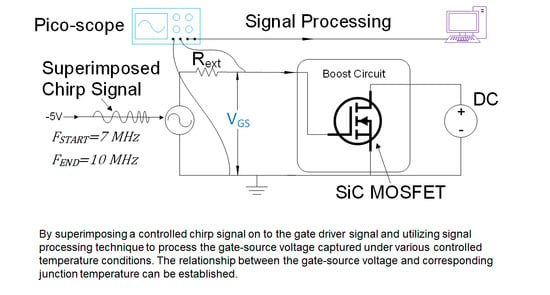
3. Principle of the Proposed TSEP

This section describes how the new TSEP can be applied in the laboratory environment. Linear AC chirp signals below the resonant frequency point are injected when the MOSFET is in its off state. At the time when signals are injected, the gate-source voltage V G S is captured and sampled data of V G S are processed using a windowing function and the fast Fourier transform (FFT), resulting in the spectrum of the gate-source voltage amplitude V G S . In this work, the Hamming window function has been selected and the number of frequency bins N is set to 1024. Since the time dependency of the measurements is relatively slow, the proposed approach is optimal. However, to improve the prediction performance when time variability is significant, time-frequency analysis such as Morlet wavelet can be applied. The authors in [30] proposed a new methodology for computing a time-frequency map for nonstationary signals using the continuous wavelet transform. The authors in [31] developed a new technique called least-squares wavelet analysis (LSWA) along with the toolbox based on MATLAB and Python [32], which can analyze any nonstationary signal accurately; this is the case in power electronic converters. Future work will be focused on investigating the LSWA algorithm to enhance the prediction performance in time-varying scenarios.
Figure 3 shows the principle of the proposed method schematically. The signal trends (used here for illustration) are in agreement with the experimental data presented in Section 4 and Section 5. Figure 3a clearly demonstrates that V G S is a linear function of the chirp frequency, f . Additionally, it is evident that V G S is a monotone increasing function of T j as it is influenced by R G ( i n t ) , which is the only temperature dependent parameter in the gate-source link. Therefore, V G S increases across all frequencies with increasing T j as shown in Figure 3a. However, the variation of V G S due to changes in T j are practically small and can be reduced by averaging V G S over the sweeping frequencies for each junction temperature. This results in an improved estimate of V G S for each T j . The total gate-source voltage amplitude V G S , t o t a l can be calculated as:
V G S , t o t a l ( T j ) = 1 N f = 0 N 1 V G S   ( f , T j )
where, N = 1024 is the FFT block size and the indices f represent the frequency bins.
With the help of Equation (8), V G S , t o t a l can be represented over T j   as shown in Figure 3b. Presenting V G S , t o t a l along the different junction temperatures provides the new TSEP.

4. Proposed TSEP Applied in the Laboratory Environment

To demonstrate the method described in Section 3, a CREE/Wolfspeed MOSFET was mounted on a voltage-controlled heat plate and connected as shown in Figure 4. The SiC MOSFET was biased using a TopCon Quadro programmable DC power supply. The power supply can produce a constant DC voltage of up to 600   V . The low-amplitude, high-frequency, linear chirp signal was generated by Tektronix AFG3102 function generator able to inject between 300   kHz   to 100   MHz   with a signal sweep period of 1   ms . The amplitude of the chirp signal is 600   mV . The signal generator was able to produce an offset of 5   V to ensure that the MOSFET is off during the injection period and the signal generator was set sweeping from 7 MHz to 10 MHz, which is below the 29 MHz resonant frequency. The DC blocking voltage was set to 300 V. The gate-source voltage was captured with the PicoScope 2204A-D2 from Pico Technology.
The temperature of the heat plate was changed after the gate-source voltage frequency spectrum was extracted for one temperature to produce a new set of a gate-source voltage frequency spectra. Thermal equilibrium was achieved by allowing sufficient time between changing the temperature of the heat plate and extracting the spectrum. The heatsink temperature was measured using a thermocouple. All data captured by the PicoScope was then processed using a Hamming-windowed FFT of 1024 frequency bins.
Figure 5a shows five V G S for five temperatures: 20.5, 46.4, 65.9, 88.5, and 112.9 °C. As shown all V G S magnitudes exhibit similar curve shapes over the sweeping frequencies but differ slightly from each other. For example, at 9 MHz, V G S is 2.5 mV at 20.5 °C but reduces to 2.4 mV at 112.9 °C. Applying Equation (9) across all V G S data produces Figure 5b, which illustrates various data points showing that V G S , t o t a l drops with increasing T j . The data points are linearized, and a trend line is estimated in Equation (9) and shown in the dotted curve in Figure 5b.
V G S , t o t a l = 0.3561 mV ° C × T j + 766.16   mV
To study the influence of the DC-link on the sensitivity of the junction temperature estimation, the DC biasing voltage has been doubled to 600 V. Figure 6 shows that both V G S and V G S , t o t a l show a similar trend compared to Figure 5; however, V G S has slightly higher values. For example, at 9 MHz, the value is 2.55 mV at 600 V compared to 2.5 mV at 300 V. Although, with 22.6 °C (600 V) the temperature is slightly higher compared to 20.5 °C (300 V). The increase of 0.05 mV does not come from the temperature but comes from the changes of C G D , C D S , and C G S due to the DC-link voltage increase.
Figure 7 shows V G S , t o t a l for seven different DC-link voltages. Figure 7 allows us to determine the sensitivity of the proposed TSEP (Table 2), which is 0.3561   mV / ° C at 300 V and 0.3200   mV / ° C at 600 V. The average value is 0.3368   mV / ° C , which is almost ± 5 %   against the highest and lowest sensitivity value. Figure 7 also shows an upward trend of V G S , t o t a l with increasing DC voltage. This is because the voltage dependency on the three capacitances is not linear but exponential in nature.

5. Proposed TSEP Applied in a DC/DC Converter

5.1. Integration of the Chirp Signal with the Gate Driver Circuit

The previous section demonstrated the proposed TSEP in operation, where the chirp signal feeds directly into the gate. This is useful in the laboratory, where SiC MOSFETs are not connected into a converter or in the manufacturing line of power devices (e.g., end of line testing of SiC MOSFET modules). However, once the SiC MOSFET is integrated into a power converter, a chirp signal cannot be directly injected into the gate. This is because commercially available MOSFET gate drivers are unable to produce any AC signals as they are limited to switch between a constant high signal e.g., 20 V and low signal e.g., 5 V. Therefore, the conventional gate driver must be modified so that chirp signals are superimposed during the negative gate voltage when the device is off. The principal circuit to achieve this is shown in Figure 8. In parallel to the external gate resistor, R G ( E x t ) , a high-frequency transformer is attached to connect the chirp generator V c h i r p with the gate driver circuit. The injected chirp voltage, therefore, applies across R G ( E x t ) and the in-series connected gate-source input impedance of the SiC MOSFET, Z G S , and the output impedance of the gate driver circuit Z G a t e . Figure 9 compares how V c h i r p is applied with and without the gate driver circuit. As shown in Figure 9a, which is the case without a gate driver (laboratory environment), V c h i r p is applied across R G ( E x t ) and Z G S , and V G S is measured across Z G S . Thus, using the voltage divider V G s is obtained as:
V G S = V C h i r p   Z G S / ( Z G S + Z G ( e x t ) )
Figure 9b shows the configuration when using a gate driver. V G S is now a function of Z G a t e , Z G S , and a 1 V voltage drop from the gate driver. The explanation for the voltage drop is detailed at the end of this section. V G S can be expressed as:
V G S = ( V C h i r p 1   V )   Z G S / ( Z G S + Z G a t e )
As R G ( E x t ) and Z G a t e driver have low temperature dependency, the dominating temperature dependent component remains R G ( i n t ) within Z G S .
In the experiment, the transformer was attached to the gate resistor that forms part of the Wolfram/Cree SiC MOSFET second generation (C2MTM) gate driver board. This gate driver board is a pull–push voltage gate driver. The high level is set to 20 V and the low level is set to 5 V. Both voltages are isolated due to two onboard isolated DC/DC converters RP1212D and RP1205S. The pulse width modulated signal (PWM) passes through the LED driver ACPL4800300E, which connects with the output gate driver IXDN609SI. During the off-state of the SiC MOSFET, the output impedance Z G a t e of IXDN609SI becomes resistive as the MOSFET driver of IXDN609SI is in its on-state to pull the gate to 5 V. The datasheet shows that the low state output resistance is 400 mΩ and shows low temperature dependency [33]. As the MOSFET driver is in its on-state, an on-state voltage of approximately 1 V applies. The RF transformer chosen is the Coilcraft RF transformer (part number: PWB1010L) with a bandwidth from 0.0035   MHz to 125   MHz . The impedance ratio of the primary winding against the secondary winding is 1:1 (750 µH primary/750 µH secondary). The attenuation of the transformer between 0.02   MHz to 30   MHz is approximately 0 dB, (i.e., gain of 1) [34]. According to the data sheet provided by the manufacturer, the phase and magnitude imbalances in the same frequency range are extremely close to 0   dB [35]. The RF transformer also offers isolation between the chirp generator and the gate signal.

5.2. Online Estimation

The Cree/Wolfspeed SiC MOSFET and the C2MTM modified Cree gate driver board are embedded in the Cree/Wolfspeed 8020-CRD-8FF1217P-1 boost DC/DC converter evaluation board [33]. Figure 10 shows the schematic of the boost converter and Figure 11 shows the experimental setup.
The overall test bench is presented in Figure 11a. The output of the boost converter is connected to a variable resistive load. The PWM signal is generated and controlled by using an interface board developed based on the TMS28335 DSP board as shown in Figure 11b and is sent to the Cree/Wolfspeed gate driver that forms part of the boost converter evaluation board. The SiC MOSFET is placed under the evaluation board and on a voltage-controlled heat plate (Figure 11c). The MOSFET was isolated from the heat plate with a silicon thermal pad. The heat plate has a resolution of 1 °C. The output load of the DC/DC converter can be changed between 30 and 300 Ω.
The DC/DC converter was set to operate at 20 kHz and 80% duty cycle. The amplitude for the AC chirp voltage was increased to 2 V peak-to-peak compared to the previous 600 mV peak-to-peak voltage used in the laboratory environment. This increase is essential to compensate for the impedance change. When the IXDN609SI gate driver is in its on-state, the chirp signal does not only apply across the 400 mΩ output resistance of the output driver but must also overcome the on-state voltage of the output driver, which is approximately 1 V as shown in Figure 9b. Figure 12 shows the results for V G S at 300 V DC-link voltage and Figure 13 shows V G S , t o t a l at 300 V. In order to investigate how the sensitivity varies with the DC-link voltage, the DC/DC converter was operated at three different DC-link voltage levels: 100 V, 200 V, and 300 V. V G S , t o t a l for each voltage level is also shown in Figure 13.
Due to the higher injected chirp peak-to-peak voltage of 2 V, V G S values are higher compared to the V G S values during the laboratory experiment, which was conducted at 600 mV. For example, V G S at 9 MHz is 52.5 mV (20.6 °C) (2 V chirp signal) compared to the 2.5 mV at 20.5 °C (600 mV chirp signal). The larger V G S values have a significant impact on the sensitivity of V G S , t o t a l . At 300 V, the sensitivity is 10.9375   mV / ° C using a 2 V chirp signal compared to 0.3561   mV / ° C using 600 mV. Thus, chirp signals with higher amplitudes provide better sensitivity. However, the amplitude should not be too high; otherwise the SiC MOSFET could accidentally turn on. Figure 13 shows that similar to the laboratory scenario, V ^ g s , t o t a l exhibits a linear trend across the junction temperature while it shows a shift in the y-axis direction when the DC bias voltage changes.

6. Discussion

Dynamic TSEPs are not suitable for SiC devices due to the fast-switching transients. As such, only measurements taken during the on/off time can be considered. To reduce the cost, electric parameters should be measured at the low-voltage side of the SiC MOSFET as they do not require the isolation barrier between the drain source and the controller. As presented in the literature, monitoring the variation of R G ( i n t )   provides more accurate temperature estimation. It is not possible to measure the voltage across R G ( i n t ) ; therefore, the alternative solution is to inject an AC signal operating at the gate-source resonant point. Because each MOSFET has manufacturing tolerances, the gate driver would need to be tuned for each MOSFET individually, which is not practical. The proposed method is more versatile because it does not require the measurement at the resonant frequency. In order to determine the junction temperature, the proposed technique requires the measurement of the DC-link voltage, which can be seen as a disadvantage. On the other hand, measurement of the DC-link voltage is a standard approach in any power converter system.
On the other side, it is worth noting that a spectrogram analysis yields more helpful results than a spectrum analysis. Spectrogram analysis provides a spectrum over time, but spectrum analysis does not provide time-dependent information, for example the relationship between the amplitude of the junction temperature and time, which is not needed in this study. In this paper, we employed spectrum analysis to develop a low-complexity solution that can be easily integrated with the gate driver circuit for online, junction temperature estimation. Future research could investigate a low-cost, time-frequency analysis technique to improve the accuracy of junction temperature estimation.

7. Conclusions

Conventional TSEPs measure voltages and currents within the switch. This works well for Si MOSFETs but due to noise issues, it is less effective for SiC MOSFETs. For the SiC MOSFETs, the internal gate resistor is regarded as a good TSEP, although it is practically difficult to capture. As the internal gate resistor is a component within gate-source impedance, this paper has proposed injecting chirp signals into the gate during the off-state of the MOSFET. The chirp signals are below the resonant frequency of the gate-source impedance. The gate-source frequency response has been sampled and processed using FFT. To increase the sensitivity, results from the FFT have been averaged over the chirp frequency spectrum resulting in an improved gate-source voltage amplitude estimate. As the internal gate resistor is the dominant temperature dependent element compared to all other parasitic parameters between the gate and source, the gate-source voltage amplitude estimate changes with the junction temperature of the SiC MOSFET; therefore, it can be utilized as TSEP. The technique has been implemented in two scenarios: testing at a stand-alone SiC MOSFET in the laboratory and in a DC/DC converter. In both cases, the TSEP exhibits good linearity and sensitivity properties. Results shown that the proposed TSEP is DC-link voltage dependent; thus, it requires monitoring the DC-link voltage. However, monitoring the DC-link voltage is common practice in power electronics. The work presented has been applied to a single-chip SiC MOSFET. Future research will investigate whether the same technique can also be applied to multi-chip SiC MOSFET power modules.

Author Contributions

Conceptualization, X.L.; laboratory work, X.L., V.P., M.A.-G., and C.C.; methodology: X.L., V.P., M.A.-G., C.C., X.W., and C.T.; formal analysis, X.L., V.P., M.A.-G., and C.C.; investigation, X.L., V.P., M.A.-G., and C.C.; writing—original draft preparation, X.L., V.P., M.A.-G., C.C., and X.W.; writing—review and editing, all authors; supervision, V.P., C.T., and M.A.-G. All authors have read and agreed to the published version of the manuscript.

Funding

This research received no external funding.

Institutional Review Board Statement

Not applicable. This study does not involving humans or animals.

Informed Consent Statement

Not applicable. This study does not involving humans.

Data Availability Statement

Data in this paper is not available to public.

Conflicts of Interest

The authors declare no conflict of interest.

Abbreviations

EVElectric Vehicle
DFTDiscrete Fourier Transform
FFTFast Fourier Transform
GaNGallium Nitride
IRInfrared Thermal Camera
LSWALeast-Squares Wavelet Analysis
MOSFETMetal–Oxide–Semiconductor Field-Effect Transistor
PWMPulse Width Modulated
SiSilicon
SiCSilicon Carbide
TSEPTemperature Sensitive Electrical Parameter

References

  1. Zhong, X.; Wu, X.; Zhou, W.; Sheng, K. An all-SiC high-frequency boost DC–DC converter operating at 320 °C junction temperature. IEEE Trans. Power Electron. 2014, 29, 5091–5096. [Google Scholar] [CrossRef]
  2. Rajput, P.; Malvoni, M.; Kumar, N.M.; Sastry, O.S.; Jayakumar, A. Operational Performance and Degradation Influenced Life Cycle Environmental–Economic Metrics of mc-Si, a-Si and HIT Photovoltaic Arrays in Hot Semi-arid Climates. Sustainability 2020, 12, 1075. [Google Scholar] [CrossRef] [Green Version]
  3. Yang, S.; Xiang, D.; Bryant, A.; Mawby, P.; Ran, L.; Tavner, P. Condition Monitoring for Device Reliability in Power Electronic Converters: A Review. IEEE Trans. Power Electron. 2010, 25, 2734–2752. [Google Scholar] [CrossRef]
  4. Musallam, M.; Johnson, C.M. Real-time compact thermal models for health management of power electronics. IEEE Trans. Power Electron. 2010, 25, 1416–1425. [Google Scholar] [CrossRef]
  5. Dupont, L.; Avenas, Y.; Jeannin, P.-O. Comparison of junction temperature evaluations in a power IGBT module using an IR camera and three thermosensitive electrical parameters. IEEE Trans. Ind. Appl. 2013, 49, 1599–1608. [Google Scholar] [CrossRef] [Green Version]
  6. Liu, P.; Chen, C.; Zhang, X.; Huang, S. Online Junction Temperature Estimation Method for SiC Modules With Built-in NTC Sensor. CPSS Trans. Power Electron. Appl. 2019, 4, 94–99. [Google Scholar] [CrossRef]
  7. Gonzalez, J.O.; Alatise, O.; Hu, J.; Ran, L.; Mawby, P.A. An Investigation of Temperature-Sensitive Electrical Parameters for SiC Power MOSFETs. IEEE Trans. Power Electron. 2017, 32, 7954–7966. [Google Scholar] [CrossRef] [Green Version]
  8. Liao, X.; Li, H.; Hu, Y.; Huang, Z.; Song, E.; Xiao, H. Analysis of SiC MOSFET dI/dt and its temperature dependence. IET Power Electron. 2017, 11, 491–500. [Google Scholar] [CrossRef]
  9. Mandeya, R.; Chen, C.; Pickert, V.; Naayagi, R.T.; Ji, B. Gate–Emitter Pre-threshold Voltage as a Health-Sensitive Parameter for IGBT Chip Failure Monitoring in High-Voltage Multichip IGBT Power Modules. IEEE Trans. Power Electron. 2019, 34, 9158–9169. [Google Scholar] [CrossRef] [Green Version]
  10. Chen, C.; Pickert, V.; Al-Greer, M.; Jia, C.; Ng, C. Localization and Detection of Bond Wire Faults in Multichip IGBT Power Modules. IEEE Trans. Power Electron. 2020, 35, 7804–7815. [Google Scholar] [CrossRef] [Green Version]
  11. Chen, Z.; Boroyevich, D.; Burgos, R. Experimental parametric study of the parasitic inductance influence on MOSFET switching characteristics. In Proceedings of the 2010 International Power Electronics Conference-ECCE ASIA-, Sapporo, Japan, 21–24 June 2010; pp. 164–169. [Google Scholar]
  12. Lemmon, A.; Mazzola, M.S.; Gafford, J.; Parker, C. Stability Considerations for Silicon Carbide Field-Effect Transistors. IEEE Trans. Power Electron. 2012, 28, 4453–4459. [Google Scholar] [CrossRef]
  13. She, X.; Huang, A.Q.; Lucia, O.; Ozpineci, B. Review of Silicon Carbide Power Devices and Their Applications. IEEE Trans. Ind. Electron. 2017, 64, 8193–8205. [Google Scholar] [CrossRef]
  14. Stella, F.; Pellegrino, G.; Armando, E.; Dapra, D. Online Junction Temperature Estimation of SiC Power mosfets Through On-State Voltage Mapping. IEEE Trans. Ind. Appl. 2018, 54, 3453–3462. [Google Scholar] [CrossRef]
  15. Li, L.; Ning, P.; Zhang, N.; Wen, X. An exploration of thermo-sensitive electrical parameters to estimate the junction temperature of silicon carbide mosfet. In Proceedings of the 2017 IEEE Transportation Electrification Conference and Expo, Asia-Pacific (ITEC Asia-Pacific), Harbin, China, 7–10 August 2017; pp. 1–5. [Google Scholar] [CrossRef]
  16. Stella, F.; Pellegrino, G.; Armando, E.; Dapra, D. Advanced testing of SiC power MOSFET modules for electric motor drives. In Proceedings of the 2017 IEEE International Electric Machines and Drives Conference (IEMDC), Miami, FL, USA, 21–24 May 2017; pp. 1–8. [Google Scholar] [CrossRef] [Green Version]
  17. Zhang, Q.; Yang, Y.; Zhang, P. A Novel Method for Monitoring the Junction Temperature of SiC MOSFET On-line Based on On-state Resistance. In Proceedings of the 2019 22nd International Conference on Electrical Machines and Systems (ICEMS), Harbin, China, 11–14 August 2019; pp. 1–5. [Google Scholar] [CrossRef]
  18. Wang, Z.; Shi, X.; Tolbert, L.; Wang, F.; Liang, Z.; Costinett, D.; Blalock, B.J. A high temperature silicon carbide mosfet power module with integrated silicon-on-insulator-based gate drive. IEEE Trans. Power Electron. 2015, 30, 1432–1445. [Google Scholar] [CrossRef]
  19. Hologne, M.; Bevilacqua, P.; Allard, B.; Clerc, G.; Morel, H.; Razik, H.; Barriere, A.; Karode, V.; Devadass, N. An experimental approach to the health-monitoring of a silicon carbide MOSFET-based power module. In Proceedings of the 2017 IEEE International Electric Machines and Drives Conference (IEMDC), Miami, FL, USA, 21–24 May 2017; pp. 1–7. [Google Scholar] [CrossRef]
  20. Griffo, A.; Wang, J.; Colombage, K.; Kamel, T. Real-Time Measurement of Temperature Sensitive Electrical Parameters in SiC Power MOSFETs. IEEE Trans. Ind. Electron. 2018, 65, 2663–2671. [Google Scholar] [CrossRef] [Green Version]
  21. Du, M.; Xin, J.; Wang, H.; Ouyang, Z.; Wei, K. Estimating Junction Temperature of SiC MOSFET Using Its Drain Current During Turn-On Transient. IEEE Trans. Electron Devices 2020, 67, 1911–1918. [Google Scholar] [CrossRef]
  22. Zhang, Z.; Wang, F.; Costinett, D.J.; Tolbert, L.M.; Blalock, B.J.; Wu, X. Online junction temperature monitoring using turn-off delay time for silicon carbide power devices. In Proceedings of the 2016 IEEE Energy Conversion Congress and Exposition (ECCE), Milwaukee, WI, USA, 18–22 September 2016; pp. 1–7. [Google Scholar] [CrossRef]
  23. Denk, M.; Bakran, M. An IGBT Driver Concept with Integrated Real-Time Junction Temperature Measurement. In Proceedings of the PCIM Europe 2014, International Exhibition and Conference for Power Electronics, Intelligent Motion, Renewable Energy and Energy Management, Nuremberg, Germany, 20–22 May 2014; pp. 1–8. [Google Scholar]
  24. Lu, X. Online Junction Temperature Estimation of SiC Power MOSFETS. School of Engineering, Newcastle University, Newcastle upon Tyne, UK. Available online: https://www.ncl.ac.uk/engineering/staff/profile/volkerpickert.html (accessed on 7 August 2021).
  25. Cree. C2M0080120D Silicon Carbide Power Mosfet Datasheet; 4600 Silicon Drive, Cree, Inc.: Durham, NC, USA, 2014. [Google Scholar]
  26. Huang, J.; Corzine, K.A.; Belkhayat, M. Small-Signal Impedance Measurement of Power-Electronics-Based AC Power Systems Using Line-to-Line Current Injection. IEEE Trans. Power Electron. 2009, 24, 445–455. [Google Scholar] [CrossRef]
  27. Blackburn, D. Temperature measurements of semiconductor devices—A review. In Proceedings of the Twentieth Annual IEEE Semiconductor Thermal Measurement and Management Symposium (IEEE Cat. No. 04CH37545), San Jose, CA, USA, 11 March 2004; pp. 70–80. [Google Scholar]
  28. Avenas, Y.; Dupont, L.; Khatir, Z. Temperature Measurement of Power Semiconductor Devices by Thermo-Sensitive Electrical Parameters—A Review. IEEE Trans. Power Electron. 2011, 27, 3081–3092. [Google Scholar] [CrossRef] [Green Version]
  29. Chemandy Electronics. Round Wire Inductance Calculator. Available online: https://chemandy.com/calculators/round-wire-inductance-calculator.htm (accessed on 30 October 2019).
  30. Sinha, S.; Routh, P.S.; Anno, P.D.; Castagna, J.P. Spectral decomposition of seismic data with continuous-wavelet transform. Geophysics 2005, 70, P19–P25. [Google Scholar] [CrossRef]
  31. Ghaderpour, E.; Pagiatakis, S.D. Least-Squares Wavelet Analysis of Unequally Spaced and Non-stationary Time Series and Its Applications. Math. Geol. 2017, 49, 819–844. [Google Scholar] [CrossRef]
  32. Ghaderpour, E. JUST: MATLAB and python software for change detection and time series analysis. GPS Solut. 2021, 25, 85. [Google Scholar] [CrossRef]
  33. IXYS. IXD_609 9-Ampere Low-Side Ultrafast MOSFET Drivers. Available online: https://www.ixysic.com/home/pdfs.nsf/www/IXD_609.pdf/$file/IXD_609.pdf (accessed on 25 October 2017).
  34. Coilcraft. PWB1010-1LC Wide-Band RF Transformer 1:1 0.03-250 MHz Datasheet. Available online: https://www.mouser.co.uk/ProductDetail/Coilcraft/PWB1010-1LC?qs=ZYnrCdKdyeeLEU%252bd2fZp%252bw== (accessed on 7 August 2021).
  35. Cree/Wolfspeed. KIT8020CRD8FF1217P-1 CREE Silicon Carbide MOSFET Evaluation Kit. Available online: https://media.digikey.com/pdf/Data%20Sheets/CREE%20Power/KIT8020CRD8FF1217P-1_UM.pdf (accessed on 6 August 2015).
Figure 1. Impedances measurement on unbiased SiC MOSFET using a network analyzer [24]. Reprinted with permission from Ref. [24]. Copyright 2019 Newcastle University.
Energies 14 04912 g001
Figure 2. Off-state equivalent circuit of a SiC MOSFET.
Energies 14 04912 g002
Figure 3. Methodology of the proposed technique to establish T j from chirp signals. (a) V G S vs. f; (b) V G S , t o t a l vs. T j .
Energies 14 04912 g003
Figure 4. Schematic of the test circuit.
Energies 14 04912 g004
Figure 5. Applying a chirp frequency between 7 and 10 MHz to a 300 V biased SiC MOSFET. (a) Gate-source voltage amplitude; (b) total peak gate-source voltage.
Energies 14 04912 g005
Figure 6. Applying a chirp frequency between 7 and 10 MHz to a 600 V biased SiC MOSFET (a) Gate-source voltage amplitude; (b) total peak gate-source voltage.
Energies 14 04912 g006
Figure 7. Comparison of DC biasing conditions for small AC chirp injection.
Energies 14 04912 g007
Figure 8. Principal schematic of applying a chirp signal into a gate driver.
Energies 14 04912 g008
Figure 9. Schematic (a) without gate driver; (b) with gate driver.
Energies 14 04912 g009
Figure 10. Schematic of the Cree/Wolfspeed boost converter evaluation board.
Energies 14 04912 g010
Figure 11. Boost converter test setup: (a) overall test bench; (b) TMS28335 PWM generating board; (c) test rig inside view.
Energies 14 04912 g011aEnergies 14 04912 g011b
Figure 12. Gate-source voltage amplitude V G S   at 300 V DC-link.
Energies 14 04912 g012
Figure 13. V G S , t o t a l as a function of T j and DC-link voltage in a fully operating DC/DC converter.
Energies 14 04912 g013
Table 1. Small-signal equivalent circuit parameters.
ParameterValue
Lead resistance ( R S L R G L ) 14.6   m Ω 14.6   m Ω
Lead inductance ( L S L L G L ) 5   nH 5   nH
Internal gate resistance ( R G ( I n t )) 4.6   Ω   @ 25   ° C [24]
Gate-Source capacitance ( C G S ) 943.5   pF   @ 600   V   [24]
Single bond wire resistance ( R S B R G B ) 12.6   m Ω 12.6   m Ω  
Single bond wire inductance ( L S B L G B ) 15   nH 15   nH
Table 2. Sensitivity of V G S , t o t a l   at different DC biasing.
DC Biasing Voltage V G S , t o t a l
50   V 0.3340   mV / ° C
100   V 0.3398   mV / ° C
200   V 0.3381   mV / ° C
300   V 0.3561   mV / ° C
400   V . 0.3465   mV / ° C
500   V 0.3235   mV / ° C
600   V 0.3200   mV / ° C
Publisher’s Note: MDPI stays neutral with regard to jurisdictional claims in published maps and institutional affiliations.

