1. Introduction
Voltage measurements in medium- and high-voltage power grids require a device that lowers the voltage to a level acceptable for measurement systems and safe for their operators. This task is performed using either voltage transformers (VTs) or cascaded capacitive voltage dividers (CCVDs). These devices have some disadvantages, especially when used in a power quality (PQ) measurement scenarios or a smart grid operation. They are large and heavy, thus limiting the number of voltage measurement locations. Another disadvantage of VTs and CCVDs is their poor frequency response. This issue was observed as early as in the late 1970s [
1], and the development of correction techniques followed [
2]. Research of frequency responses and the development of correction methods continue to this day. Studies show that both VTs [
3] and CCVDs [
4] are limited in a frequency band to a few kHz at best, and even less when using resonance dampers. Various frequency response correction techniques have been proposed [
5]. The broad and known frequency response of a transceiver has become more important recently, as the number of power electronic loads and sources in the power grid increases significantly. This situation may lead to the occurrence of phase and frequency jumps, which have to be processed by a voltage converter with reasonably low uncertainty. New research in this topic includes an application of jump resonance systems, among others, in frequency monitoring devices [
6].
Alternative medium- and high-voltage measurement techniques have been developed. Some solutions are commercially available, while others still exist only in a research domain. One of the most popular devices, other than the aforementioned, is a resistive divider. It offers a wide frequency band and high precision but does not provide insulation from a measured voltage. This feature makes resistive dividers unsafe to operate and limits their application to special cases only. Another solution is an application of an electro–optic (Kerr or Pockels) effect. Measurement devices utilizing this effect have been under development since the 1960s [
7,
8]. These devices are commercially available and offer a wide frequency band, but due to their low sensitivity, they are limited to measurements of pulses and transient phenomena.
Yet another medium- and high-voltage measurement technique is through the use of electric field sensors located around live wires, usually on the ground below a transmission line. This measurement method is under active research [
9,
10,
11], but thus far, it has not reached commercial availability. The advantage of using field sensors is that there is no need for a direct connection to wires. This improves the portability of the measurement system. The main drawback of this solution is that it is hard to calibrate, as each sensor processes the electric field emanating from all wires. To overcome this limitation, methods limited to analysis of relative values only have been developed, such as phase sequence detection [
12] or distortion measurement [
13].
The goal of the research presented in this paper was to develop a medium- and high-voltage sensor that has the following features:
It is small and installed directly on a wire;
It provides wide frequency band;
It does not need a complex calibration procedure.
Development is supported by finite element method simulations and a simple laboratory experiment, which is meant to provide a proof of concept.
Installation directly on a live wire makes a sensor similar to a current sensor installed on a wire, such as the ones described in [
14,
15,
16,
17,
18]. It would be complementary to such sensors because it would allow us to create a complete power and energy measurement system to be installed on a wire without requiring a ground connection.
The remaining part of the paper is divided into four sections. In the next section, a detailed description of the sensor is provided, supported by theoretical reasoning. The following section describes the purpose and methodology of a performed finite element method (FEM) simulation. The section then presents and discusses FEM simulation results. The next section describes the laboratory model of a sensor and a setup used for experiments, followed by a description of the experiments themselves, presentation of results, and discussion. The paper closes with a summary section, discussing overall results and plans for future research.
2. Sensor Construction
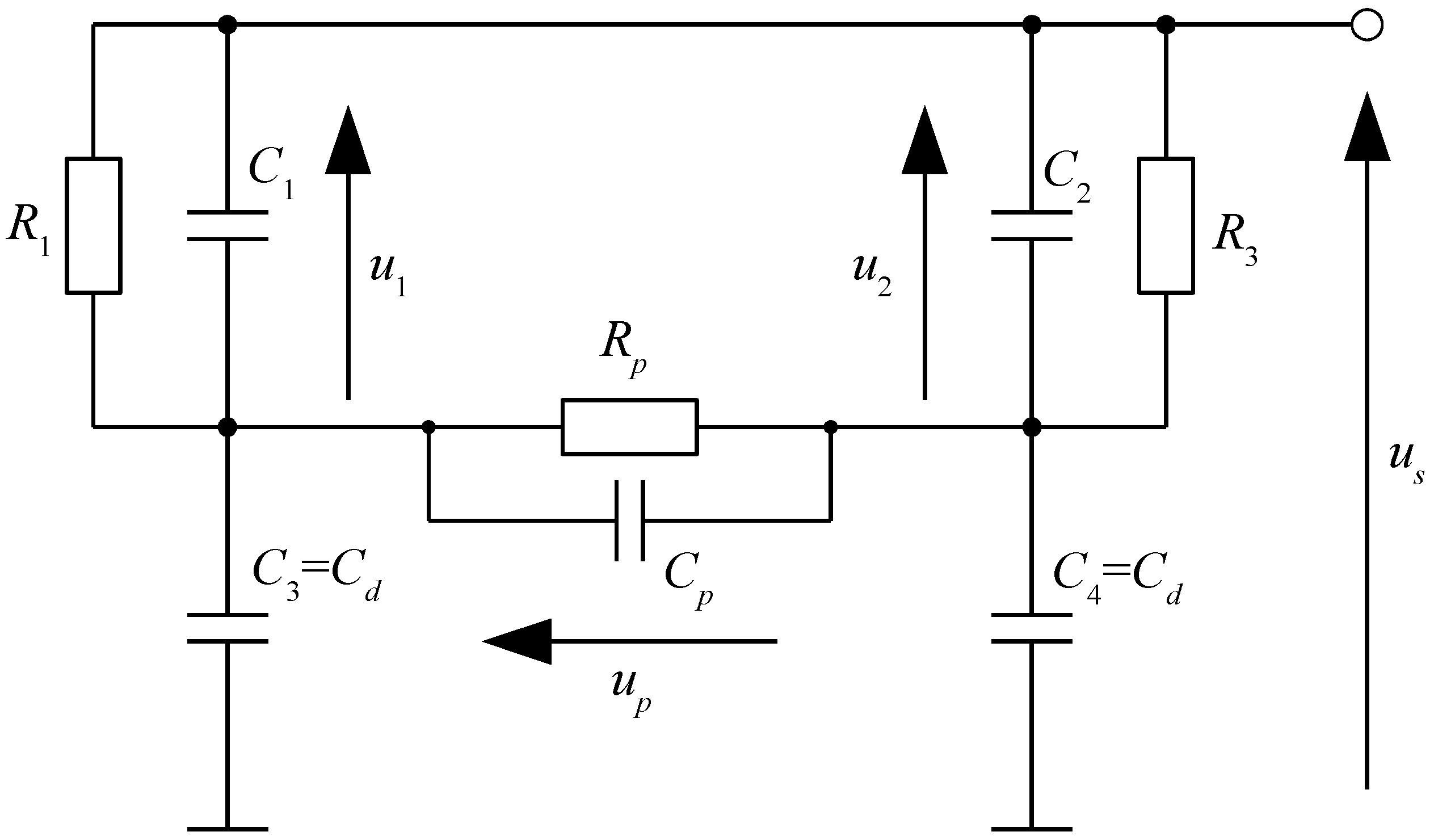
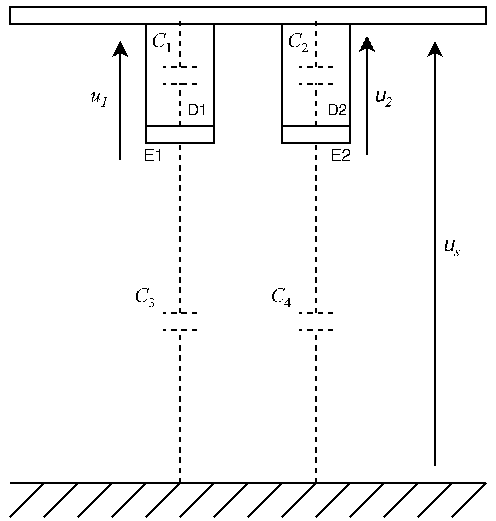
Our proposed sensor consists of two nonconductive elements that are attached to a live busbar or wire, with a separate electrode installed at the end of each element. This arrangement creates a capacitive bridge structure from an electrical point of view. A diagram that juxtaposes a mechanical construction and an electrical diagram of the sensor is presented in
Figure 1.
In this diagram, D1 and D2 are dielectric elements, while the electrodes are marked E1 and E2. The capacitances between electrodes and busbars are and . The capacitances between electrodes and the ground are marked and . Input voltage is marked , while sensors output voltages are and .
The concept of the sensor calls for making capacitances
and
equal to each other while keeping
and
different.
Output voltages
and
are then described with the following equations:
These equations can be used to calculate both input voltage
and ground capacitance
as follows:
Hence, the proposed sensor can be used to convert a voltage without the need for on-site calibration.
The main technical problem with this configuration is how to ensure the fulfillment of Equation (
1) and inequality (
2) at the same time. For Equation (
1) to be true, elements D1, D2, E1, and E2 have to be made the same size and installed close to each other. With identical dimensions of D1 and D2, the only way to ensure that (
2) is true is to make D1 and D2 from materials that have different dielectric permeability coefficients (
).
Impact of Data Readout Circuitry
To measure voltage, a data readout circuitry has to be added to the sensor. This will have an impact on the sensor’s operation because it adds load to the relatively small capacitances of a bridge. Two cases were analyzed:
Only voltages and are measured directly, while is calculated;
All three voltages are measured directly.
The circuit diagram for both cases is presented in
Figure 2. Resistive elements
,
, and
represent the internal resistances of the inputs of the measurement devices that we used, which will normally be inputs of operational amplifiers. Capacitance
represents the input capacitance of an amplifier that converts voltage
. The input capacitances of the other two amplifiers do not need to be explicitly included because they add to capacitances
and
.
In the first case, elements
and
from
Figure 2 are omitted in the calculation. The equations that describe a ground capacitance and derivative of an input voltage are the following:
where
and
. As these conductances approach 0, the equations will simplify to Equations (
3) and (
4). Note that besides the result for the input voltage equation being a derivative, both equations require derivatives of sensor output voltages to be included. In this case, the derivatives are directly measured at sensor outputs, and values of
and
have to be calculated by integration.
In the second analyzed case, elements
and
from
Figure 2 are included in the calculation. This makes the circuit a full bridge. Equations for a ground capacitance and derivative of an input voltage take the following form:
Again, when conductances
,
,
, and capacitance
approach 0, these equations convert to Equations (
3) and (4). Note how adding elements
and
significantly increases the complexity of the equations. Hence, although voltage
can be measured directly, its measurement does not improve the operation of the sensor in a valuable manner.
3. Finite Element Method Simulations
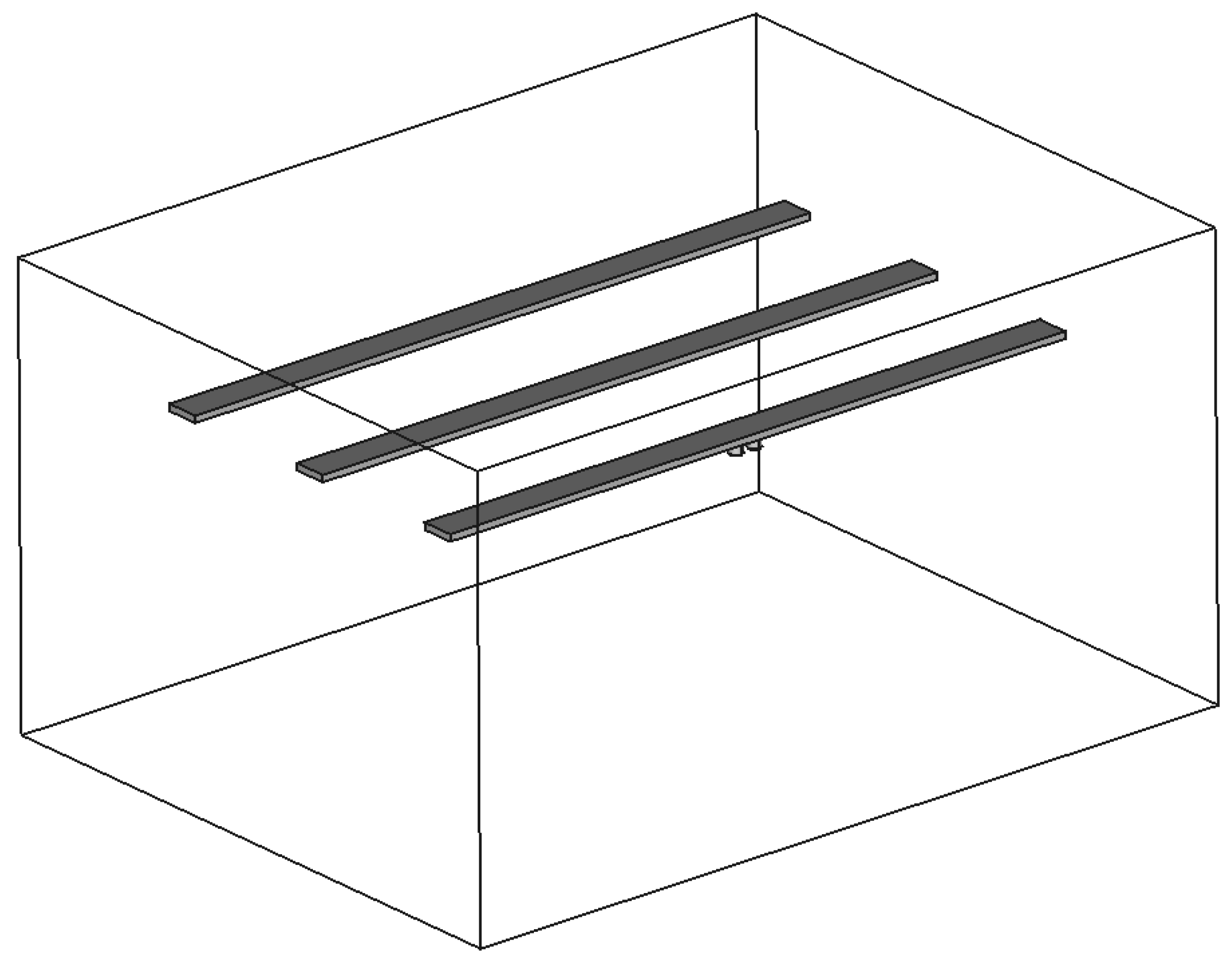
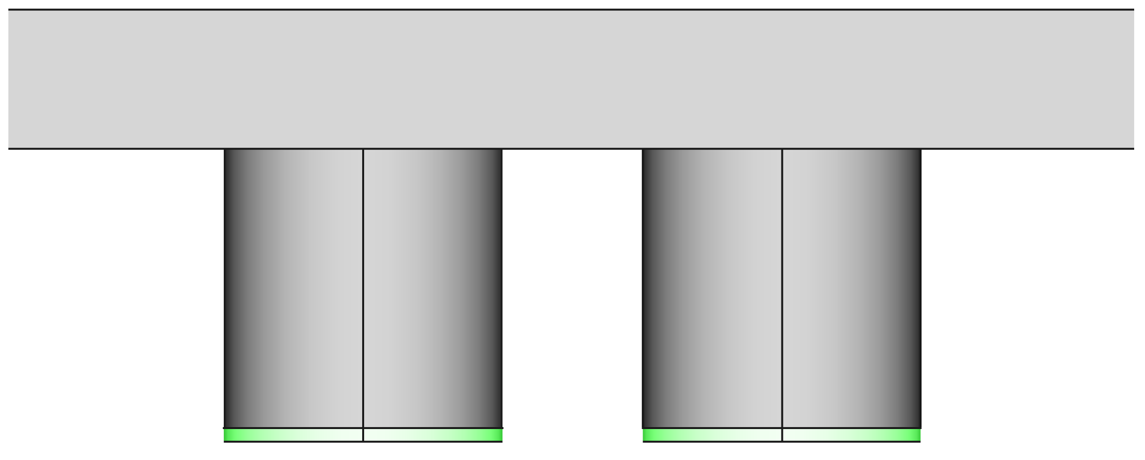
A finite element method (FEM) simulation was performed to confirm the proposed idea and to obtain quantitative information before constructing a laboratory model. Hence, the goal of a FEM simulation was to calculate capacitances
and
and their dependency on materials of D1 and D2 elements. A three-dimensional model of a three-phase indoor medium-voltage station was created for the FEM experiments. This model contains a cuboid envelope with dimensions 1200 by 900 by 640 mm (x, y, and z, respectively), and three busbars modeled as cuboid elements 1000 by 50 by 10 mm in size. The model of the sensor has been placed on the bottom of one of the busbars. A perspective view of the model with an envelope represented as a wire-frame is presented in
Figure 3.
The sensor model contains two dielectric cylindrical elements with both diameter and length of 20 mm, ended with flat (1 mm thick) conductive electrodes. Additional elements (e.g., readout electronics, communication cables, or supporting insulators) were omitted for clarity because they were not important for this simplified simulation.
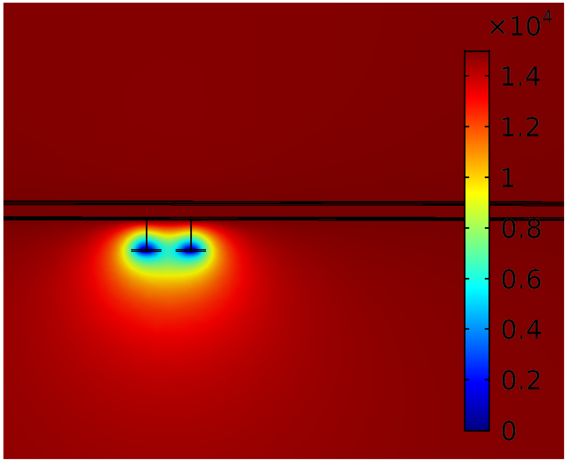
Figure 4 presents a close-up of a sensor model located on busbar 1 of a substation model.
Two cases were simulated using COMSOL Multiphysics:
Case a, “low ”, where elements D1 and D2 have = 3 and = 2, respectively. This is similar to the case that would be used for the experiments;
Case b, “high ”, where D1 and D2 have have = 20 and = 10, respectively. This represents a much better scenario that is still achievable with off-the-shelf materials such as glass.
Simulation Results
Figure 5 presents an example of calculated electric field potentials within elements D1 and D2. The calculated capacitances between busbar and electrodes are as follows:
For case a, = 2.01 pF and = 1.13 pF;
For case b, = 5.65 pF and = 3.68 pF.
It is worth noting that despite much higher permeability coefficients of materials for case b, the actual capacitances are not much higher than in case a. By the ratio of alone, one would expect case b capacitance to be 6.7 times higher than calculated for case a. A value of a calculated for case b would theoretically be five times greater than for case a. The actual results give capacitance ratios of 2.81 and 3.26 for and , respectively. These differences are caused by capacitive couplings between busbar and electrode forming in dielectric materials used and in the surrounding air. Higher capacitances can be achieved by making elements D1 and D2 relatively short and wide (“pancake shaped”) rather than long and thin (“cylinder shaped”).
4. The Experiment
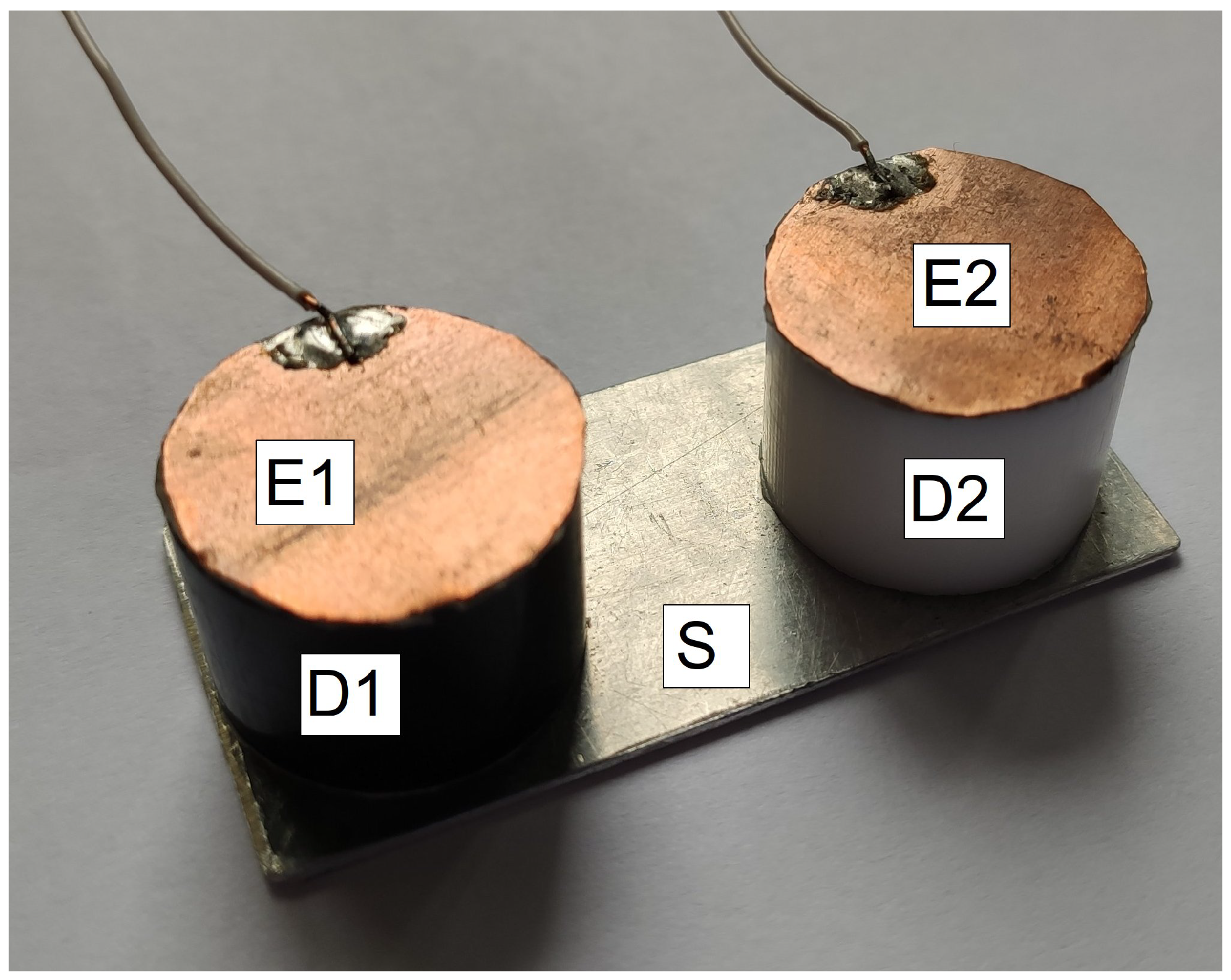
A laboratory experiment with medium voltage was performed as a proof of concept. It was also used to detect eventual sensor drawbacks and deficiencies. For the experiment, a laboratory model of a sensor was built. This sensor is presented in
Figure 6. It consists of solid dielectric cylinders forming elements D1 and D2, which were glued to an aluminum plate to form a connection electrode. Electrodes E1 and E2 were made from an adhesive copper foil, which allows for easy soldering of contacts.
Element D1 (black in the photo) was made from polyoxymethylene (POM), which has a dielectric constant
= 3.7 [
19]. Element D2 (white) was made from polytetrafluoroethylene (Teflon, PTFE), which has
= 2 [
20]. These materials were chosen because they were readily available and easy to work with mechanically. These values are similar to those from the FEM simulation case a.
Before connecting readout electronics, the capacitances of a laboratory model were measured using an Agilent E4980A RLC meter. The following results were obtained:
= 2.79 pF;
= 2.40 pF.
Note that the ratio is only 1.1625, which is even less than the value obtained in FEM simulations. In addition, input capacitances of amplifiers will add to these capacitances evenly, making the ratio even lower.
4.1. Laboratory Substation
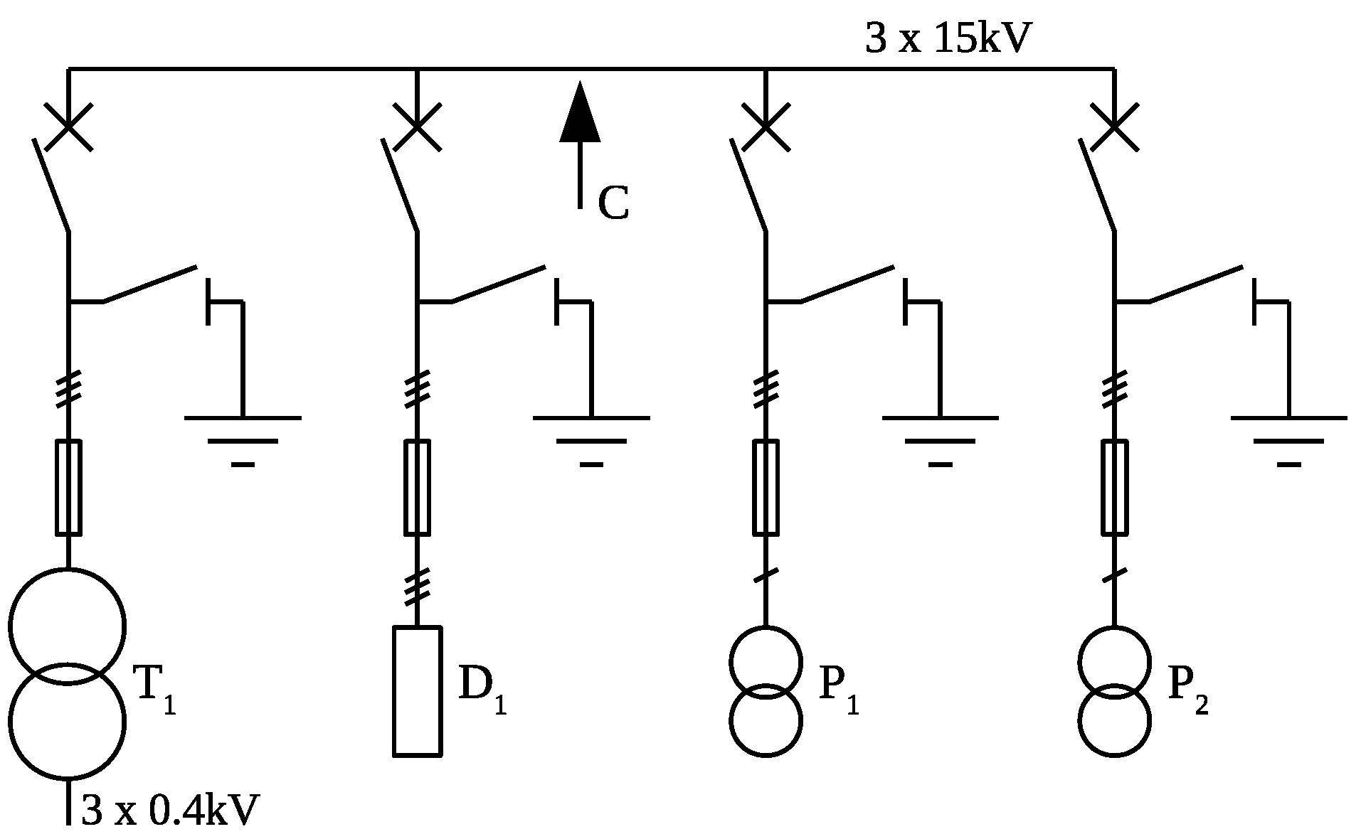
The experiment was performed in a laboratory medium-voltage substation. It has a nominal voltage of 15 kV (phase to phase), which is delivered by a step-up transformer. This allows an operator to power a substation with an easily controllable low voltage. During the experiment, the substation was powered with a manually controlled voltage using an autotransformer.
A schematic diagram of a substation is presented in
Figure 7. It has four sections. The first section contains the aforementioned step-up transformer. In the second section, there are three resistive voltage dividers, type VD30-12.5Y-A-KB-A made by Ross inc. These dividers provide uncertainty of 1% in the 1 MHz frequency band. The third section contains a class 0.2 laboratory voltage transformer that can be connected to one selected phase. This device was not used in experiments. The last section of the substation is left empty to install any device under test. However, because the tested sensor was meant to be installed directly on a busbar, it was not installed in the fourth section. Instead, it was mounted in a top compartment, containing substation busbars. The approximate location of the sensor is marked by an arrow in
Figure 7.
4.2. Voltage Acquisition and Data Transmission System
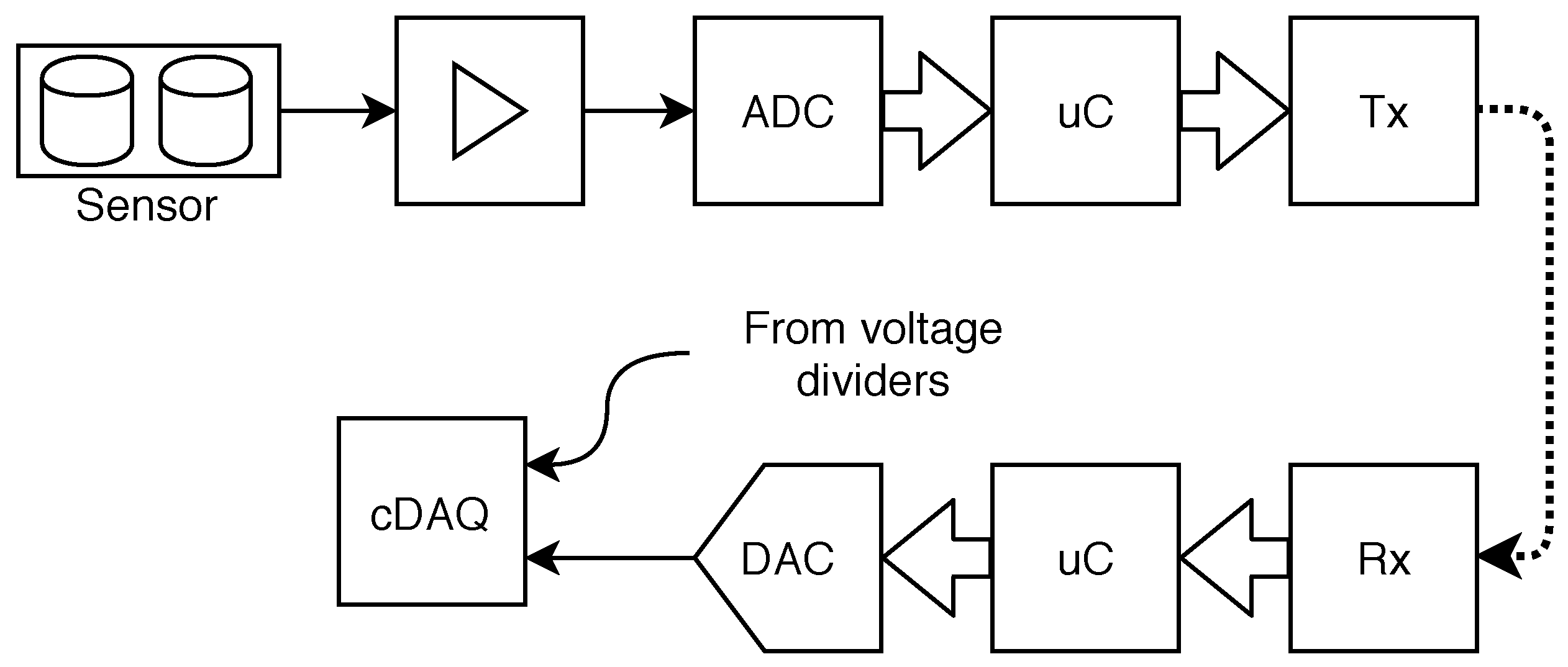
A system for voltage acquisition and data transmission was constructed specifically for the experiment. Its block diagram is presented in
Figure 8. It consists of the sender and receiver parts.
The sender part consists of two input amplifiers and a microcontroller. Input amplifiers have FET inputs and operate in a noninverting configuration, with one amplifier input connected to each electrode and a common ground of the sender connected to a live busbar. Amplifier inputs add 1 pF capacitance (added to and ) and 6 T parallel resistance ( and ) to each sensor electrode. Besides providing amplification and impedance matching, amplifiers also shift voltage by 2.5 V to match the A/D converter operating with a single supply. The Microcontroller used in experiments was Microchip PIC16F18426, selected for its availability and our knowledge in programming this series. It used an internal 12-bit A/D converter to convert voltages from amplifier outputs. Data were then sent over a simplex (transmit and clock only) SPI interface. SPI pins of the microcontroller directly drive fiber-optic transmitters. Both transmitters are model HFBR-1522Z, designed to operate with a 2 mm plastic fiber-optic cable. The cable used for transmission was a simple plastic multimode cable designed for short-range, low-cost applications. It was suitable for this application as only 3 m were needed, and a described configuration supports transmission up to 40 m. Use of relatively low-speed A/D converters, interface, and limiting fiber-optic cable limited bandwidth of the whole system. It was, however, considered enough for a proof of concept experiment. As a sender operates on a medium-voltage busbar, it can not take a mains supply. Two 6F22 9 V batteries powered the sender during experiments. Of course, in the case of actual application in long–term experiments, an energy harvesting system has to be developed for the sensor.
The receiver contains two fiber-optical receivers (HFBR-2522Z) connected to a microcontroller of the same type as in the sender (PIC16F18426). The reuse of a microcontroller simplified the programming. Microcontroller received data over SPI bus and drove two 10-bit D/A converters using I2C bus. This way, sensor electrode voltages were reconstructed in an analog form at the low-potential side. Such a solution is not optimal, as it introduces both noise and some nonlinearities, which caused issues discussed later in the text. It allowed us, however, to speed up development by using a ready data acquisition system with analog inputs, which was available on-site. This data acquisition system was a National Instruments cDAQ device, equipped with four ±10 V analog inputs (among other inputs and outputs not used in the experiment).
4.3. Results
The experiment consisted of recording both sensor input and output voltages for various values of input voltage (up to 4 kV). The acquired voltages were then processed offline using MATLAB. First, momentary values were calculated from Equation (
7). These were used to calculate RMS values over 0.25 s periods. RMS values were then used to calculate the errors over an entire measured range, as well as to calculate static nonlinearities. Frequency spectra were calculated from a steady section of momentary values, using an FFT algorithm. The spectra were then used to check the harmonic content of input and output voltages and calculate THD+N coefficients.
4.3.1. Momentary Values
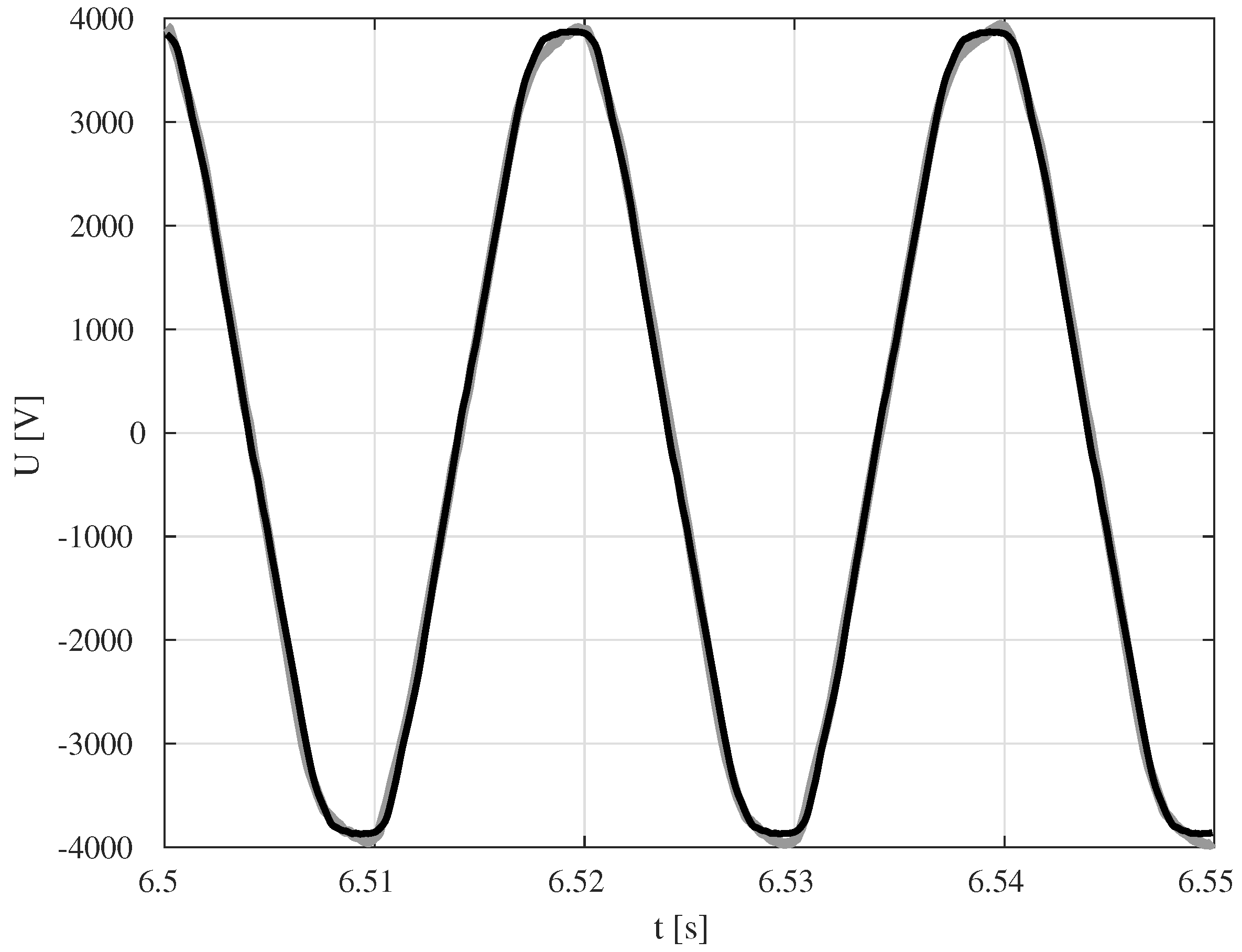
The waveforms of momentary values of input and output voltages are presented in
Figure 9. A sensor output voltage follows the momentary value of input voltage closely but not perfectly. Asymmetrical peaks suggest an introduction of even harmonic components that are absent in the input voltage.
4.3.2. RMS Errors
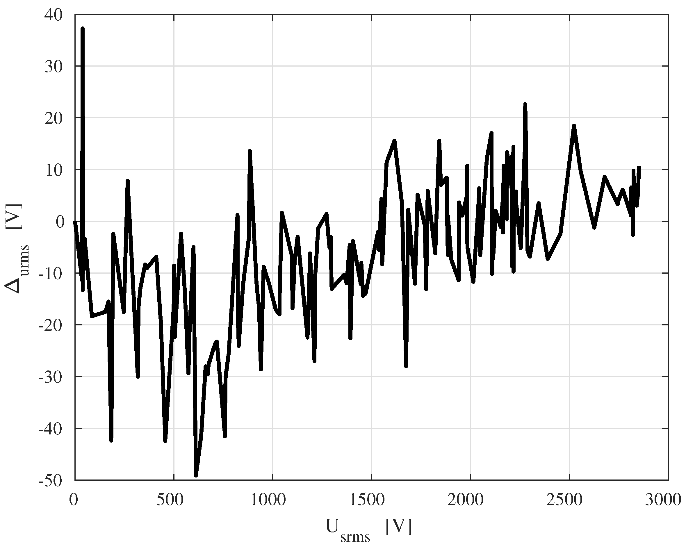
RMS errors were calculated by subtracting RMS values of input and output. Their dependency on input voltage is presented in
Figure 10. Note that relative errors are high in a range below 1 kV, where absolute errors stay around 40 V while an input voltage drops. A more in-depth analysis of the transmitted signals shows that a major component of RMS errors comes from sampling errors of a voltage acquisition and data transmission system.
4.3.3. Static Linearity
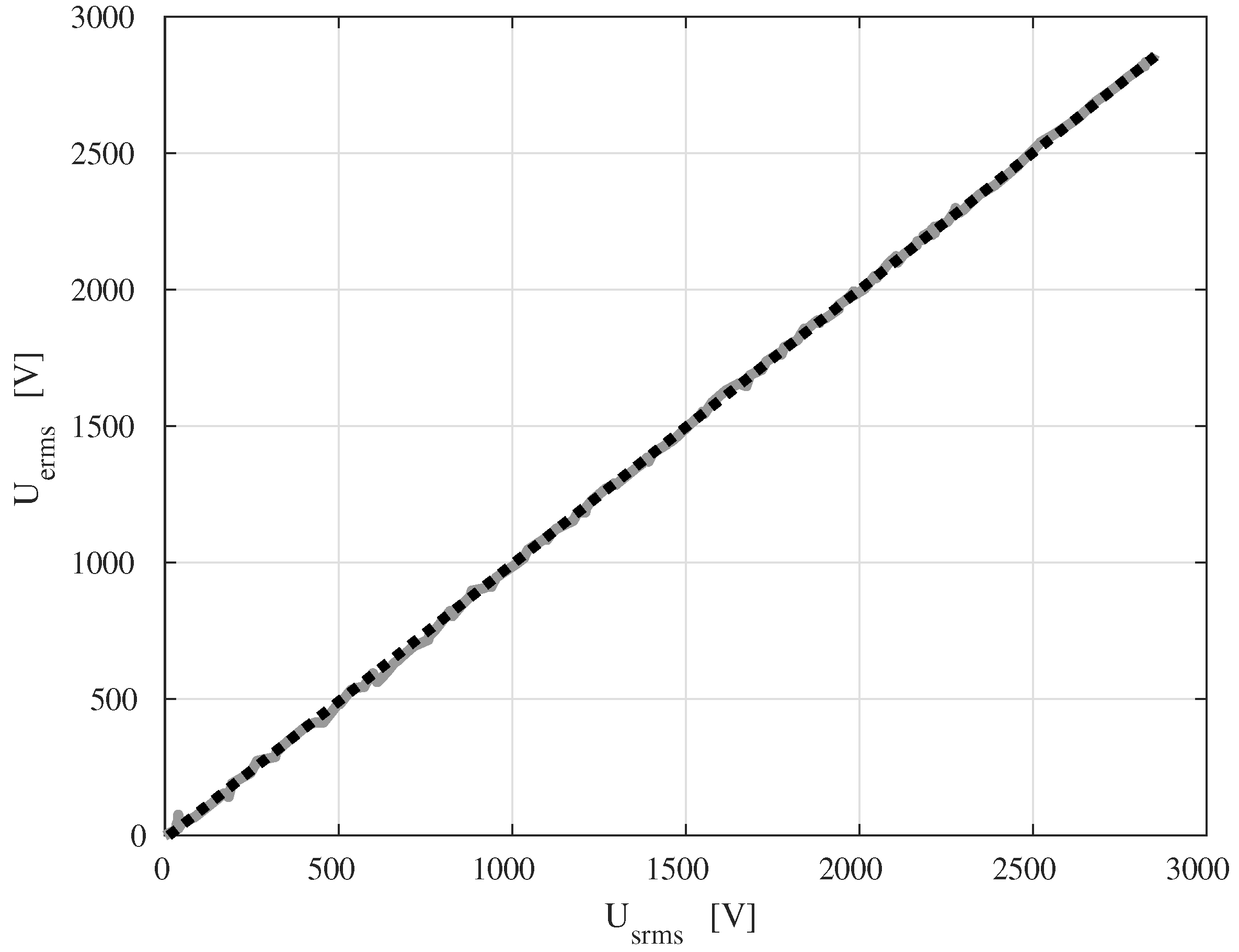
Input vs. output RMS characteristic is presented in
Figure 11. This figure shows that the sensor is generally linear within a tested voltage range. However, the sensor exhibited some nonlinearity in a low voltage range. This has again been attributed to the low quality of the voltage acquisition and data transmission system, rather than with the sensor itself.
4.4. Frequency Spectra
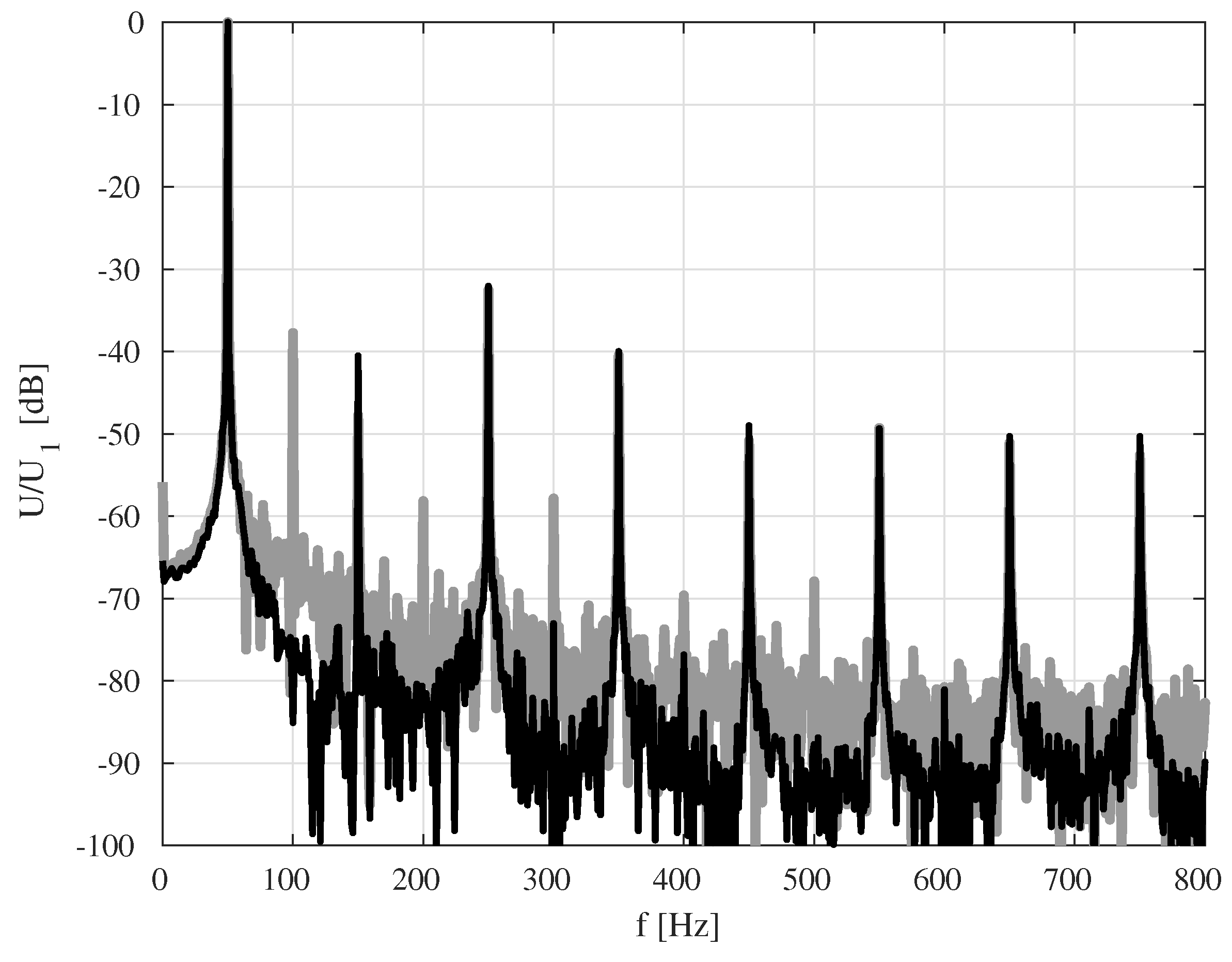
The frequency spectra of input and output voltages are juxtaposed in
Figure 12. A range of 0 to 800 Hz is presented because there were barely any components above this frequency. A decibel scale relative to the first harmonic was used to emphasize higher harmonic components. The first harmonic component of input voltage was around 4 kV.
The spectrum of the output voltage (gray in the figure) showed a prominent presence of even harmonic components, which are not present in an input voltage. This was expected after analysis of momentary values that show characteristically asymmetrical peaks (
Figure 9). In addition, background noise is slightly higher (around 10 dB). To obtain quantitative values of introduced disturbance, the following values of THD+N were calculated:
THD+N() = 3.019%;
THD+N() = 3.097%.
These values indicate an additional 0.07% of THD+N introduced by the sensor and its accompanying circuitry. The sensor itself does not contain any components that would be nonlinear in this voltage range. Hence, the (over)simplified voltage acquisition and data transmission system is the main suspect when it comes to introducing nonlinearities and noise.
4.5. Ground Capacitance Estimation
Besides voltage analysis, ground capacitance
was estimated using Equation (8). The obtained value is 3.966 pF and is relatively constant over the whole experiment, varying by ±0.532 fF which corresponds to 0.01344% of calculated
. This variation is probably caused by a slight difference between
and
. Note that the actual uncertainty of the estimation is higher than the aforementioned variation; this occurs because
and
function as reference values in this measurement. These capacitances were measured outside the substation; therefore, the presence of a busbar was not taken into account. Moreover, amplifier input capacitances that add to
and
, as described in
Section 2, were only taken into account as catalog values. However, the low variability of a calculated
shows that a reliable estimation of
can be performed using the sensor. When used with overhead lines, this feature may be used for line diagnostics by analyzing the changes of ground capacitance that increase when a line hangs lower due to, for example, overheating.
5. Conclusions
In this paper, a novel voltage sensor construction has been presented. The proposed sensor consisted of two dielectric elements that were made from different materials, which were used to obtain different dielectric constants. This allowed us to even out the ground capacitances by using the same shape for both elements while obtaining usable signals from the sensor electrodes.
The main purpose of this paper was to present the sensor and its proof of concept; consequently, FEM simulations were performed to check the viability and to obtain the capacitance values that were needed for later experiments. The obtained results prove the sensor to be technically viable, but it needs high-impedance amplifiers to measure the electrode voltages.
The experiments that we conducted proved that the sensor can be a reliable device for measuring medium voltages and ground capacitance of sensor electrodes. This proves the proposed concept. The voltage values and calculated metrics that we obtained are satisfactory for a preliminary construction that is meant only as a proof-of-concept experiment. The system developed for voltage acquisition and data transmission proved to be the most problematic element of the system. It was oversimplified, and as a result, it introduced nonlinearities and noise to transmitted voltages.
Overall, the presented sensor construction is unique in the way that it can be used together with an online current sensor, forming a complete power analysis system. However, there are still some issues that are not yet resolved, including powering the sensor and its accompanying electronics, reliable measurement, or calculation of internal capacitances after installation, and data transmission. These issues will be considered in future research.
Author Contributions
Conceptualization, A.W. and A.B.; methodology, A.W. and M.P.; software, A.W.; validation, M.P. and A.W.; formal analysis, A.W.; investigation, A.W., A.B. and M.P.; resources, A.B.; data curation, A.W. and M.P.; writing—original draft preparation, A.W.; writing—review and editing, A.B.; visualization, M.P.; supervision, A.W.; project administration, A.W.; funding acquisition, A.B. All authors have read and agreed to the published version of the manuscript.
Funding
This research received no external funding.
Institutional Review Board Statement
Not applicable.
Informed Consent Statement
Not applicable.
Data Availability Statement
Data, schematic diagrams for laboratory models and source code available on request. Please contact a corresponding author.
Conflicts of Interest
The authors declare no conflict of interest.
References
- Olivier, G.; Bouchard, R.P.; Gervais, Y.; Mukhedkar, D. Frequency Response of HV Test Transformers and the Associated Measurement Problems. IEEE Trans. Power Appar. Syst. 1980, PAS-99, 141–146. [Google Scholar] [CrossRef]
- Douglass, D.A. Potential Transformer Accuracy at 60HZ Voltages Above and Below Rating and at Frequencies Above 60 Hz. IEEE Trans. Power Appar. Syst. 1980, PAS-100, 1370–1375. [Google Scholar] [CrossRef]
- Cox, M.D.; Berry, F.C.; Govindarajan, S.N. Harmonic response tests on distribution circuit potential transformers. IEEE Trans. Power Deliv. 1991, 6, 973–978. [Google Scholar] [CrossRef]
- Jian, L.; Hao, Z.; Chao, G.; Qian, Z. Harmonic voltage measurement error of the capacitor voltage transformer. PLoS ONE 2018, 13, 1–26. [Google Scholar]
- da Silva, C.A.; Fernandes, D.; Neves, W.L.A.; Machado, E.P. Coupling Capacitor Voltage Transformer: A Device to Correct its Secondary Voltage in Real Time. J. Control Autom. Electr. Syst. 2013, 24, 339–348. [Google Scholar] [CrossRef]
- Bucolo, M.; Buscarino, A.; Fortuna, L.; Frasca, M. Multiple Hysteresis Jump Resonance in a Class of Forced Nonlinear Circuits and Systems. Int. J. Bifurc. Chaos 2020, 30, 2050258. [Google Scholar] [CrossRef]
- Wunsch, D.C.; Erteza, A. Kerr cell measuring system for high voltage pulses. Rev. Sci. Instrum. 1964, 35, 816–820. [Google Scholar] [CrossRef]
- Santos, J.C.; Taplamacioglu, M.C.; Hidaka, K. Pockels high-voltage measurement system. IEEE Trans. Power Deliv. 2000, 15, 8–13. [Google Scholar] [CrossRef]
- Simkin, D.C.; Gerrard, A.; Gibson, J.R.; Jones, G.R.; Holt, L. Measurements of power system voltages using remote electric field monitoring. IEEE Proc. Online 1998, 10, 142–149. [Google Scholar]
- Wu, L.; Wouters, P.A.A.F.; Van Heesch, E.J.M.; Steennis, E.F. On-site voltage measurement with capacitive sensors on high voltage systems. In Proceedings of the 2011 IEEE Trondheim Power, Trondheim, Norway, 19–23 June 2011. [Google Scholar]
- Borkowski, D.; Wetula, A.; Bień, A. Contactless Measurement of Substation Busbars Voltages and Waveforms Reconstruction Using Electric Field Sensors and Artificial Neural Network. IEEE Trans. Smart Grid 2015, 6, 1560–1569. [Google Scholar] [CrossRef]
- Li, F.; Moore, P.J. Determination of phase sequence and voltage level of high-voltage double-circuit overhead conductors using non-contact technique. In Proceedings of the 2006 IEEE Power Engineering Society General Meeting, Montreal, QC, Canada, 18–22 June 2006. [Google Scholar]
- Chen, K.; Yang, X.; Xu, W. Contactless Voltage Distortion Measurement Using Electric Field Sensors. IEEE Trans. Smart Grid 2018, 9, 5643–5652. [Google Scholar] [CrossRef]
- Falvo, M.C.; Grasselli, U.; Lamedica, R.; Lampasi, D.A.; Maranzano, G.; Podest’a, L. PQ Events Measurement in an Electrified Metro-Transit System, IVT Influence Analysis. In Proceedings of the 9th International Conference on Probabilistic Methods Applied to Power Systems, KTH, Stockholm, Sweden, 11–15 June 2006. [Google Scholar]
- Campbell, B.; Dutta, P. Gemini: A Non-invasive, Energy-Harvesting True Power Meter. In Proceedings of the 2014 IEEE Real-Time Systems Symposium, Rome, Italy, 2–5 December 2014. [Google Scholar]
- Wang, W.; Huang, X.; Tan, L.; Guo, J.; Liu, H. Optimization design of an inductive energy harvesting device for wireless power supply system overhead high-voltage power lines. Energies 2016, 9, 242. [Google Scholar] [CrossRef]
- Porcarelli, D.; Brunelli, D.; Benini, L. Clamp-and-measure forever: A Mosfet-based circuit for energy harvesting and measurement targeted for power meters. In Proceedings of the 5th IEEE International Workshop on Advances in Sensors and Interfaces IWASI, Bari, Italy, 13–14 June 2013. [Google Scholar]
- Porcarelli, D.; Brunelli, D.; Benini, L. Clamp-and-Forget: A self-sustainable non-invasive wireless sensor node for smart metering applications. Microelectron. J. 2014, 45, 1671–1678. [Google Scholar] [CrossRef]
- Luftl, S.; Chandran, S. (Eds.) Polyoxmetylene Handbook: Structure, Properties, Applications, and Their Nanocomposites; Scrivener Publishing LLC: Beverly, MA, USA, 2004; ISBN 978-1-118-38511. [Google Scholar]
- Ho, P.S.; Leu, J.; Lee, W.W. (Eds.) Low Dielectric Constant Materials for IC Applications. In Springer Series in Advanced Microelectronics; Springer: Berlin, Germany, 2003; ISBN 978-3-642-55908-2. [Google Scholar]
| Publisher’s Note: MDPI stays neutral with regard to jurisdictional claims in published maps and institutional affiliations. |
© 2021 by the authors. Licensee MDPI, Basel, Switzerland. This article is an open access article distributed under the terms and conditions of the Creative Commons Attribution (CC BY) license (https://creativecommons.org/licenses/by/4.0/).


