Article

Application of Scattering Parameters to DPL Time-Lag Parameter Estimation at Nanoscale in Modern Integration Circuit Structures

Department of Microelectronics and Computer Science—DMCS, Lodz University of Technology, 90-924 Lodz, Poland
*
Author to whom correspondence should be addressed.
Energies 2021, 14(15), 4425; https://doi.org/10.3390/en14154425
Submission received: 15 June 2021 / Revised: 28 June 2021 / Accepted: 20 July 2021 / Published: 22 July 2021
(This article belongs to the Special Issue Thermal Management and Characterization in Electronics)

Abstract

:
This paper presents the methodology of material parameters’ estimation for the dual-phase-lag (DPL) model at the nanoscale in modern integration circuit (IC) structures. The analyses and measurements performed were used in the unique dedicated micro-electro-mechanical system (MEMS) test structure. The electric and thermal domain of this structure was analysed. Finally, the silicon dioxide (SiO2) temperature time-lag estimation procedure is presented based on the scattering parameters measured by a vector network analyser for the considered MEMS structure together with the 2-omega method. The proposed methodology has the ability to estimate the time-lag parameter with high accuracy and is also suitable for the temperature time-lag estimation for other manufacturing process technologies of ICs and other insulation materials used for integrated circuits such as silicon nitride (Si3N4), titanium nitride (TiN), and hafnium dioxide (HfO2).

1. Introduction

The modelling and analysis of thermal and electromagnetic phenomena in integrated circuits (ICs) have great significance for the reliable design of modern nanoscale electronic structures and micro-electro-mechanical systems (MEMSs). It is also highly recommended to use this approach during various design-related activities. The most important of them are as follows: continuous decrease of semiconductor technology nodes, design cost reduction of microelectronic systems, and application of modern transistors in ICs (e.g., a fin field-effect transistor—FinFET [1,2], a gate-all-around field-effect transistor—GAAFET [3], and a vertical-slit field-effect transistor—VeSFET [4]).
Therefore, the presented work focuses on the following issues:
  • The effective modelling and simulation methods of electromagnetic (EM) and thermal phenomena of integration circuits, micro-electro-mechanical systems (MEMSs), and 3D integrated systems (see [1,5]).
  • The design of an equivalent electric circuit extractor and electrical simulation tools, e.g., [2,6,7].
  • The verification of new simulation tools dedicated for the design of experimental application specific integrated circuits (ASICs).
  • Estimation of IC material parameters for the nanometric technologies.
The first and last issues will be presented in the paper and are performed on scattering parameters measurements of a designed MEMS test structure with a printed circuit board (PCB) test board.

2. Heat Transfer at the Nanoscale

The heat transfer problems in solids can be described using Fourier’s theory [8,9]. The mathematical description is based on Fourier’s law and the Fourier–Kirchhoff (FK) equation and can be expressed as follows:
{ c v T ( x , t ) t = · q ( x , t ) + q v ( x , t ) q ( x , t ) = k · T ( x , t )   for   x R n , n N , t R + { 0 }
where q is heat flux vector; k is material thermal conductivity; T is distributed temperature; and cv and qV are volumetric heat capacity and value of internally generated heat, respectively. The FK equation has been commonly used to describe heat flow for over two centuries. However, the application of the FK equation has some significant limitations at the nanoscale [10].
The main limitation is related to the assumption of the infinite heat flow velocity in the semiconductor structure, which is very important in the case of nanostructures with a Knudsen number of Kn < 0.1 (where the characteristic length of IC is ca. ten times longer than the heat carrier mean free path 41.8 nm at 300 K [8]). Furthermore, the simultaneous change of temperature gradient and heat flux is a non-physical behaviour [9,10,11,12,13]; these phenomena have been presented in the case of nanosized structures in [8]. The second problem is associated with the radiative heat transfer and the Casimir effect (i.e., photons tunnelling) [14,15]; these phenomena occur in MEMSs [16] at small distances between surfaces (or particles). Both phenomena cause more dynamic and intense heat transfer than the classical Fourier–Kirchhoff and radiation models.
The new and more general dual-phase-lag (DPL) model of heat flow in solids at the nanoscale was introduced by Tzou [17,18] and is described with the following equations:
{ c v T ( x , t ) t = · q ( x , t ) + q v ( x , t ) q ( x , t ) + τ q q ( x , t ) t = k T ( x , t ) τ T k T ( x , t ) t
or
τ q c v 2 T ( x , t ) t 2 + c v T ( x , t ) t = k Δ T ( x , t ) + τ T k Δ T ( x , t ) t + q v ( x , t ) + τ q q v ( x , t ) t
where τT and τq are temperature time-lag and heat flux time-lag, respectively. The simplified version of the DPL heat transfer model can be obtained for one time-lag parameter τq for τq > 0 and τT = 0. This equation was proposed by Cattaneo and Vernotte (CV) in [19,20,21,22,23,24,25,26] and is also used to eliminate the paradox of the heat-flux infinite velocity transfer.
The comprehensive presentation of the DPL model aspects is included in the following published sources:
  • Modified boundary conditions, the DPL model simplification, and numerically effective 3D harmonic temperature models’ representation were presented in [1];
  • Internal heat generation source analysis and its realistic approximation were presented in Appendix A and [19] (pp. 12–13 in Appendix A);
  • Detailed analysis of anomalies and intriguing behaviours of the CV, DPL, and FK models were discussed by Vermeersch and De Mey, as well as Kovács and Ván, in [1,27,28,29] and [25];
  • Material parameters are collected in [1,30];
  • Detailed description of the most commonly used heat transfer models at the nanoscale was presented in [16] (pp. 1–4) [22,23,24,30].
The DPL model can be used to describe heat transfer behaviour in various solid materials (e.g., metals, bulk crystals, dielectrics, and amorphous materials). For most of them, indicative dual-phase time-lag parameters values (τT, τq) can be approximated using theoretical formulas [1]. Unfortunately, these parameters are strictly dependent on material density, fractal dimensions of material structure [30], and so on. Therefore, the values of the time-lag parameters should be empirically and independently characterised for each IC and MEMS technology process types. It is possible to perform empirical measurements of their values using a unique tool based on the femtosecond pulse laser with reflection mirrors for the following:
  • Thin metals (Brorson et al. [31,32]; Elsayed-Ali [33]; and Qiu et al. [34,35,36,37]);
  • No crystalline and amorphous materials (Fournier and Boccara [38]).
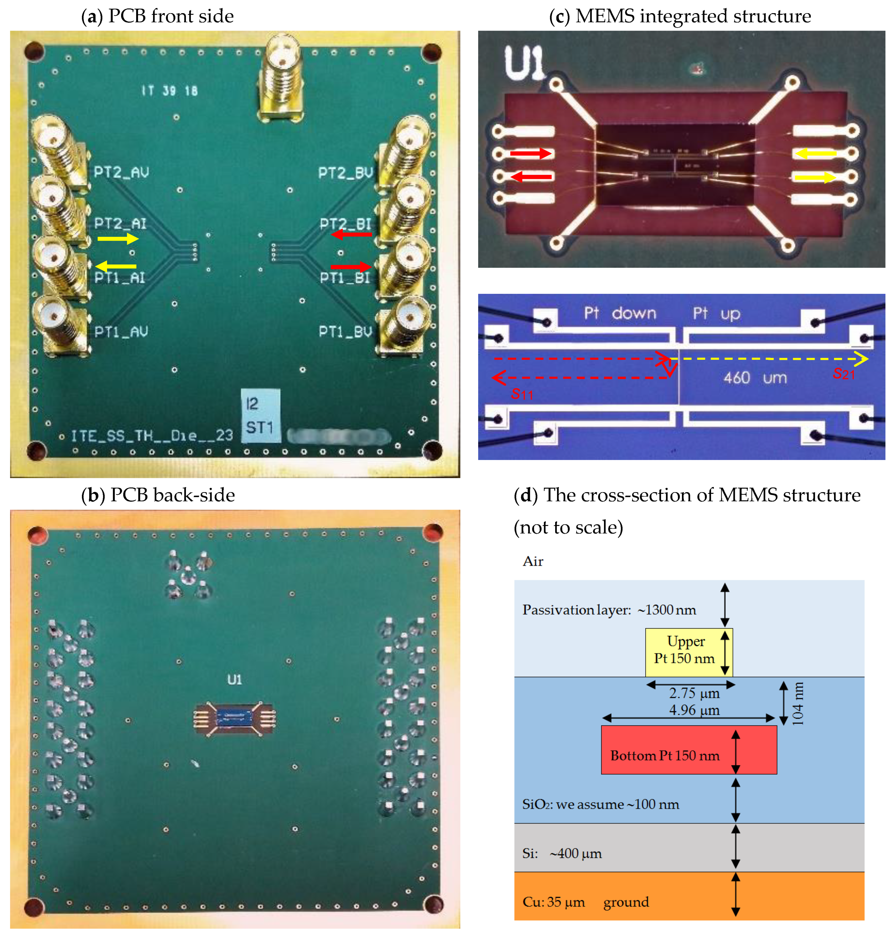
However, the test probes used for this purpose should be prepared not exactly like real structures in ICs and MEMSs. The first investigation of the dual-phase time-lag parameters estimation using dedicated MEMS structures with a measurement system implemented on a PCB was depicted in [39,40,41,42,43]. The authors of this paper propose the scattering wave parameters presented in [2] to extract the value of the dual-phase time-lag parameter τT.

3. Test Structure

The DPL model was verified using a dedicated test structure containing a 104 nm thin silicon oxide layer (SiO2: εr = 3.9 [44,45], we assume a constant value up-to 13.5 GHz based on [46]; tan δ = 0.0002 [47]) placed between two platinum resistors (the top resistor: Pt: Wtop = 2.75 μm, thickness h = 150 nm, length L = 460 μm, resistance Rtop = 155 Ω at 20 °C [39,48,49]; the bottom resistor: Pt, Wbottom = 4.96 μm, thickness h = 150 nm, length L = 460 μm, resistance Rbottom = 262.3 Ω at 20 °C [39,48,49]). Generally, each resistor could be used either as a heat source line or a temperature sensor. The bottom resistor is treated as a heater, and the upper resistor is a temperature sensor. Each resistor has a four-wire connection for independent measurements of voltage and current. These elements are placed on a 100 nm wide silicon dioxide (SiO2) layer stacked on a 400 µm thick silicon layer. The test structure presented in Figure 1c was manufactured in MEMS technology by the Institute of Electron Technology (ITE) in Warsaw, Poland [39,40,41,42,43,44,45]. The bottom and upper resistor dependence on temperature and their temperature rise dependence on heating power were measured and characterised in [39,40]. The entire structure is bonded to a metal copper foil on a PCB test board (Figure 1a,b).

4. Test Structure Models and Measurement Process

4.1. Thermal Model

The 2D DPL thermal model of the MEMS test structure is described with the application of the harmonic temperature models proposed in [1]:
{ k β   Δ T r k γ   Δ T i + g 0 2 = ω c v T i k β   Δ T i + k γ   Δ T r       = ω c v T r
β = 1 + τ T τ q ω 2 1 + τ q 2 ω 2 ; γ = ( τ T τ q ) ω 1 + τ q 2 ω 2
where T _ = T _ ( x , y , z ) = T r + j T i Z is harmonic temperature field distribution for angular frequency ω = 2πf, associated with the temperature in the following way:
T ( x , y , z , t ) = T m ( x , y , z )   sin ( ω t + φ ( x , y , z ) ) = Im [ 2   T _ ( x , y , z )   exp ( j ω t ) ]
2   T _ ( x , y , z ) = T m ( x , y , z )   exp ( j φ ( x , y , z ) )
Moreover, Tm and φ are amplitude and phase-shift for a given angular frequency, respectively. Please note that the maximal complex values of the harmonic temperature field are taken into consideration; thus, the coefficient 2 is introduced in Equations (4)–(7). The dissipated heat power generation per unit volume in the bottom resistor (g0 > 0) is described in Appendix A. The heat power generation outside the bottom resistor is equal to zero g0 = 0 W/m3. The following boundary conditions were applied:
  • The upper side of the structure—the heat-free convection is encoded using Neumann boundary condition with a heat transfer coefficient equal to 658.763 W/(m2K).
  • The left and right side of the structure—the symmetry is applied using Neumann boundary conditions.
  • The Dirichlet boundary condition for the bottom side of the structure Tr = Tambient, Ti = 0.
The material parameters are included in Table 1. In addition, calculated temperature distributions for 10 Hz, 1 kHz, 100 kHz, and 1 GHz are presented in Table 2.
As can be observed in Figure 2, the changes of temperature amplitude |T(x,y,f)| in SiO2 are located around the bottom heating resistor at f = 100 MHz and higher frequencies. Therefore, SiO2 thermal characterisation should be performed for f ≥ 100 MHz. Consequently, the simulations were carried out for the frequency in the range f = 200–900 MHz.
Values of a temperature time-lag and a heat flux time-lag for bulk SiO2 material have been proposed in the literature equal to τT ≈ 60 ns and τq ≈ 3 ns, respectively (see [1,30]). Nevertheless, we also have to determine this value for the ITE process technologies. We want to propose a methodology of the DPL time lag estimation for other insulation materials applied in the integrated circuits, such as silicon nitride (Si3N4), titanium nitride (TiN), hafnium dioxide (HfO2), and others. Thus, numerous simulations were carried out for the temperature time-lag-delay parameter in the range τT = 50–120 ns to find the estimated value.
The experiments and analyses carried out by Tomasz Raszkowski in his PhD thesis [50,51], concerning the transformation of the DPL equation into the Grünwald–Letnikov fractional space-derivative dual-phase-lag equation [16,46,47], indicate a lower influence of the heat flux time lag parameter τq for the whole thermal system response than for the temperature time lag parameter τT.
The analysis of the influence of time lag differences τT-τq [1] (pp. 140—Figure 2, pp. 143—Figures 5 and 6, pp. 142—Table 2) as well as the total thermal delay of complex IC thermal system [1] (pp. 151, see Table 6) show that the heat-flux time lag parameter is less critical than the temperature-time lag for final thermal system response. Therefore, we adopted its value equal to τq ≈ 3 ns, as proposed in the literature. Simulations were carried out and are presented in Figure 3. It can be noticed that the most significant change in the phase of temperature depending on the time-lags is recognised at the frequency range near 300 MHz and 500 MHz. However, the most significant amplitude of temperature changes on the upper resistor is observed close to the lower frequency f ≈ 300 MHz (see Figure 3a). Therefore, the highest sensitivity of time-lag estimation is at f ≈ 300 MHz. Finally, f ≈ 300 MHz frequency neighbourhood, in the range of τT = 50–120 ns and τq ≈ 3 ns, was selected as the best parameter value set for further investigation (Figure 4b).
Next, based on the collected simulation results, the linear regression was used to model the relationship between the temperature time-lag τT and the averaged phase-shift of the upper resistor temperature arg T(x,y,f). The function
τ T | f = 300 MHz = 2.391746   ( ± 0.064775 ) · arg ( T upper ) 87.07922 ( ± 4.52158 ) [ ns , ° ]
is used for the analysed MEMS test structure, which is presented in Figure 1c (τT ∈ (50 ns, 120 ns) and τq = 3 ns) with R2 = 0.999774.

4.2. Electrical Analysis and Final Measurement Procedure

The electrical behaviour or the MEMS test structure (Figure 1c) was determined using the Vector Network Analyzer PNA-X Microwave Agilent N5242A after application of the de-embedding procedure [2]. The electrical reference planes were set to the test board SMA (SubMiniature version A) connectors using Agilent N4691B Electronic Calibration Module. All non-utilised connectors were terminated. The complex scattering parameters (s11, s12, s21, s22) have to be measured at 32,000 spot frequency points in the range 10 kHz–15 GHz using 50 Ω characteristic impedance of the measurement equipment.
The analysis of the electric behaviour of the MEMS test structure (Figure 1d) and the PCB test board is based on the previous study about transmission lines presented in [2]. Therefore, the following conclusions were derived for the chosen frequency close to f ≈ 300 MHz:
  • The upper and lower resistor lengths are very short compared with the wavelength at f ≈ 300 MHz. Therefore, the distributed character of both resistors shall be taken into account for f > c/(20 L εr−1/2) ≈ 64 GHz, where c is the speed of the light in the vacuum, and the relative electric permittivity of SiO2 is equal to εr ≈ 3.9. Consequently, only a de-embedded procedure for a PCB is required for the PCB transmission lines’ elimination [2].
  • The investigation presented in [2] shows that the eddy-current losses (and skin effect) in a conductor and dielectric losses can be neglected with a 1.4% error up to 10 GHz and an error lower than 0.3% up to 2 GHz.
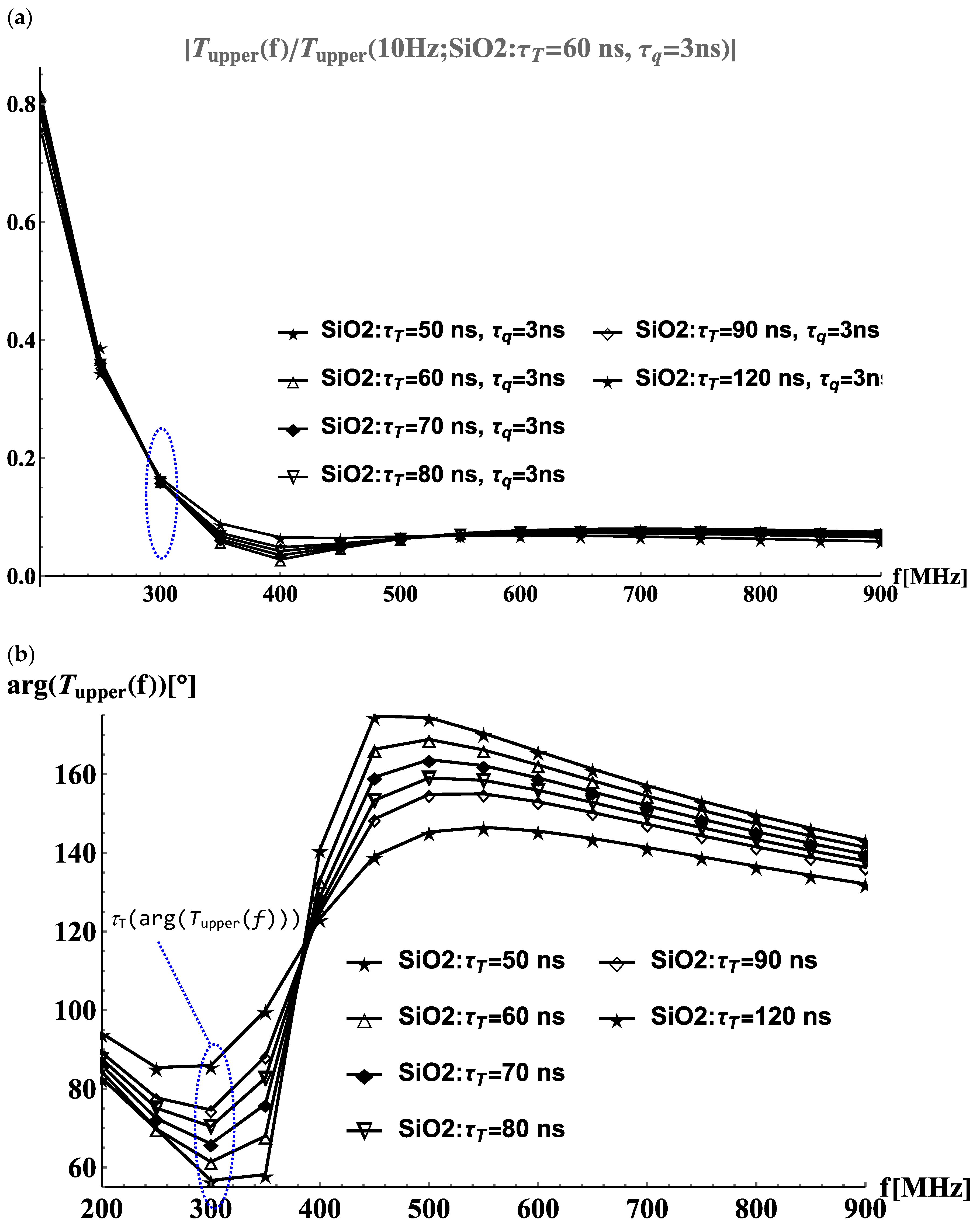
  • The extracted parasitic parameters in Table 2 show that inductance and capacitance can be neglected for f ≈ 300 MHz.
  • It should also be noted the self-heating can be neglected for a small current flowing through the platinum resistor (e.g., Ibottom ≤ 5 mA [44]).
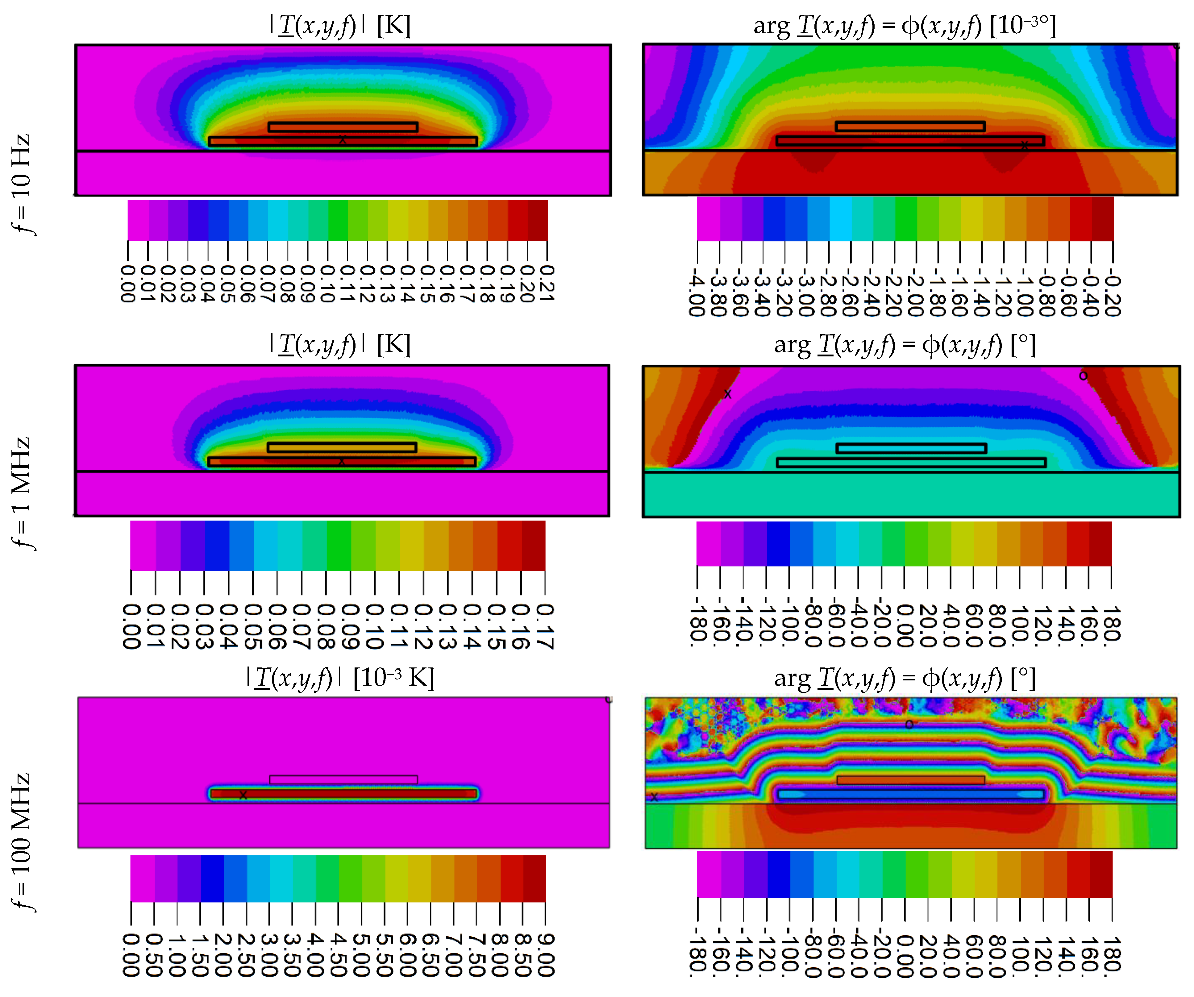
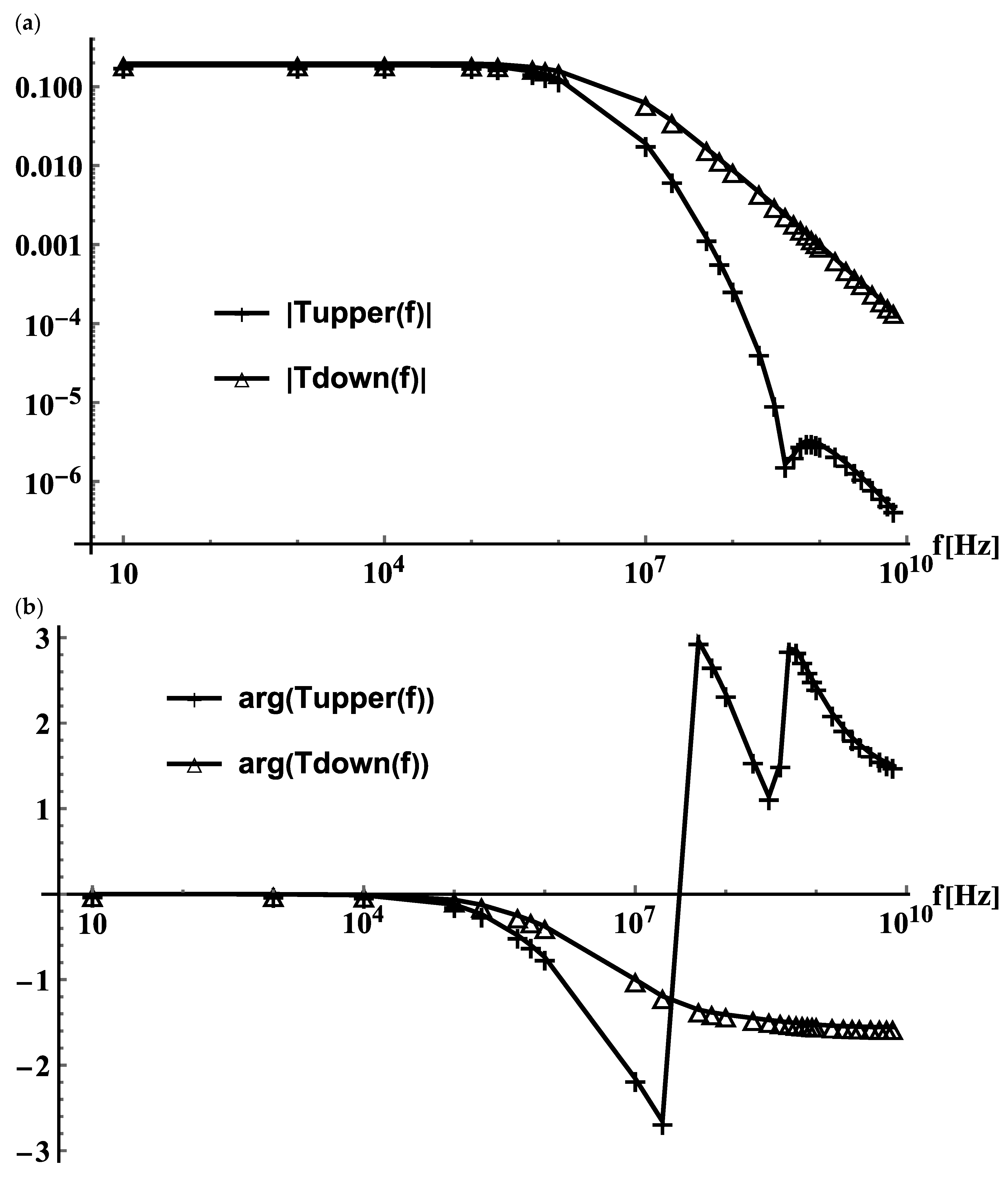
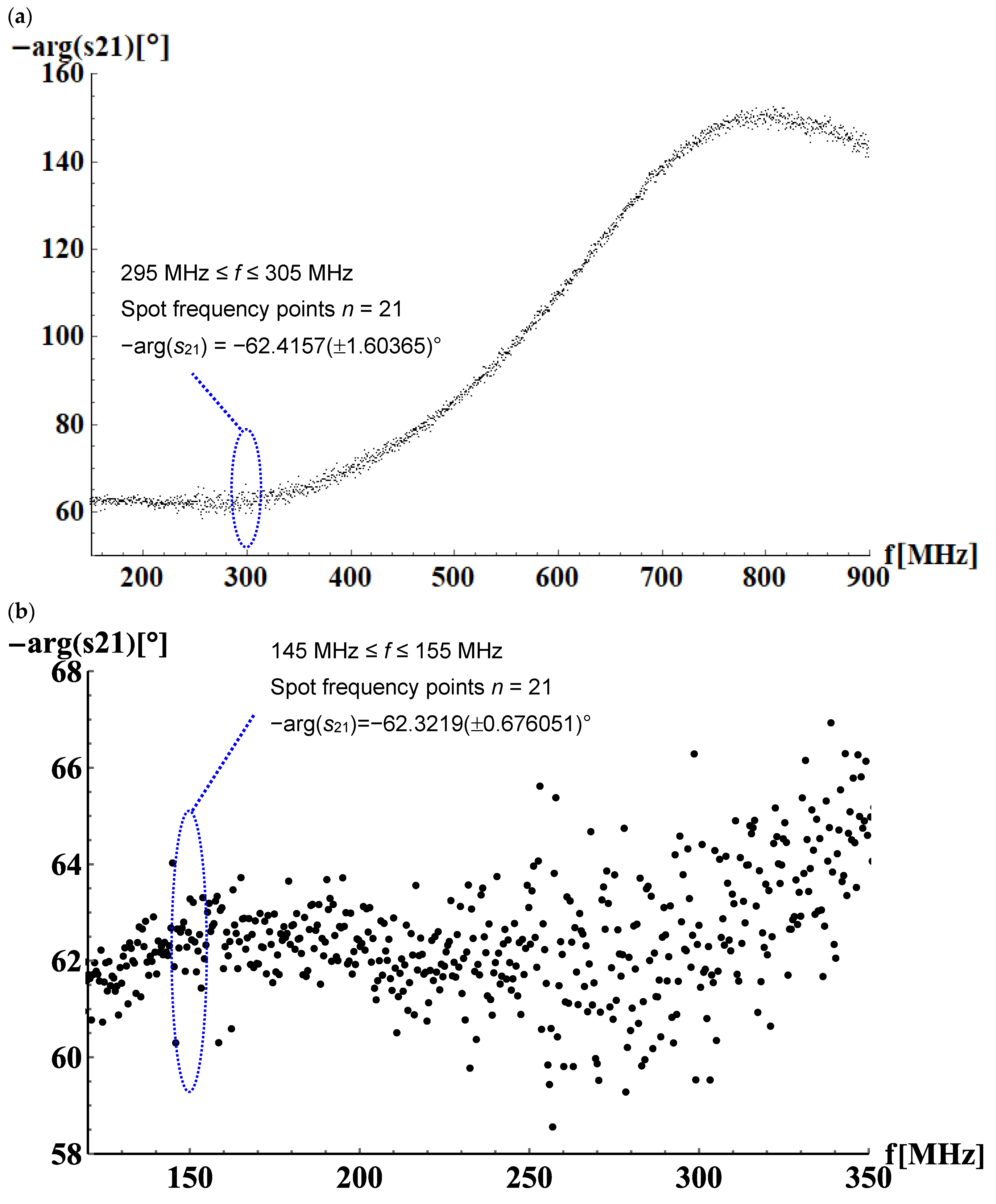
  • As can be noticed, the application of the network analyser allows for the direct measurement of the power wave transmitted through the MEMS test structure s12 = s21, which represents the insertion loss of the analysed network. To determine the temperature time-lag delay, we used the s21 measurements for a frequency close to f = 150 MHz (n = 21 spot frequency points in the range 145 MHz ≤ f ≤ 155 MHz) and determined the averaged value and standard deviation of this parameter arg(s21) = 62.3219 (±0.676051)° at f = 150 MHz, with the sum of error squares (SS) = 9.01973 and degrees of freedom (DOFs) = 21 (see Figure 5). Finally, the temperature time-lag delay can be calculated from Equation (8):
τ T = 61 . 9791 ( ± 1.61694 )   ns   at   f = 300   MHz

4.3. Results and Discussions

As can be observed in Figure 2, the changes of temperature amplitude |T(x,y,f)| in SiO2 are localised around the bottom heating resistor at f = 100 MHz and higher frequencies. Therefore, SiO2 thermal characterisation should be performed for f ≥ 100 MHz.
Based on the simulation, it can be noticed that the best scopes for which we obtain the highest sensitivity of the measurement method are the frequency range near 300 MHz to 500 MHz (see Figure 4). However, the most significant amplitude of temperature changes on the upper resistor is observed close to the lower frequency f ≈ 300 MHz (Figure 3a).
Next, based on the collected simulation results, the linear regression was used to model the relationship between the temperature time-lag τT and the averaged phase-shift of the upper resistor temperature arg T(x,y,f) in the form of a function:
τ T | f = 300 MHz = 2.391746   ( ± 0.064775 ) · arg ( T upper ) 87.07922 ( ± 4.52158 ) [ ns , ° ]
for the analysed MEMS test structure, which is presented in Figure 1c (τT ∈ (50 ns, 120 ns) and τq = 3 ns) with R2 = 0.999774.
To determine the temperature time-lag delay, we used the s21 measurements for a frequency close to f = 150 MHz and determined the averaged value and standard deviation of this parameter arg(s21) = 62.3219 (±0.676051)° at f = 150 MHz (see Figure 4). Finally, the temperature time-lag delay can be calculated from Equations (8) and (10) using scattering parameters arg(s21):
τ T = 61 . 9791 ( ± 1.61694 )   ns   at   f = 300   MHz
for Itop ≤ 5 mA and Ibottom ≤ 5 mA [44].

5. Conclusions

This paper includes electromagnetic and thermal analyses of the MEMS test structure developed to validate the DPL model based on the methodology and tools presented in [2] for electric and thermal domains [1], respectively. The detailed analysis allows determining the best measurement frequency as well as electric and thermal model simplifications. Moreover, the new approach is associated with conducting measurements of electromagnetic scattering parameters together with simplification of the EM and thermal models of the MEMS test structure.
As a final result, we used a network analyser to determine the temperature time-lag delay in SiO2 τT = 61.9791 (±1.61694) ns for assumed heat flux time-lag delay τ q = 3 ns , which is a big challenge in the case of ICs and MEMSs. The final time-lag delay values are applicable for the devices manufactured in the technology process developed by the Institute of Electron Technology in Warsaw, Poland.
The proposed method is suitable for determining the time-lag delay parameters of other materials and other technological processes of ICs, which can be very important during thermal and electro-thermal investigations of advanced electronic nano structures. The ability of high accuracy estimation of temperature distribution in the newest electronic devices is very significant for the real thermal model analysis. As a result, it is crucial for the reliability of whole nanoscale appliances in modern semiconductor structures.

Supplementary Materials

The following are available online at https://www.mdpi.com/article/10.3390/en14154425/s1.

Author Contributions

Conceptualization and methodology, M.Z.; investigation, all authors; resources, M.J. and Z.K.; writing—original draft preparation, M.Z.; writing—review and editing, M.J., Z.K. and A.N.; supervision, A.N. All authors have read and agreed to the published version of the manuscript.

Funding

The research presented in this paper was supported by both the project OPUS No 2013/11/B/ST7/01742 funded by the National Science Centre in Poland and by the internal university grant of the Lodz University of Technology.

Institutional Review Board Statement

Not applicable.

Informed Consent Statement

Not applicable.

Data Availability Statement

The data presented in this study are openly available in supplementary materials.

Acknowledgments

The authors would like to express their special thanks to M. Janicki and J. Topilko for sharing papers [39,40] and [43,44,45].

Conflicts of Interest

The authors declare no conflict of interest.

Appendix A. Analysis of Dissipated Power and Internal Heat Generation Source in MEMS Test Structure

With a limited error, we can assume that the bottom resistor of the considered MEMS test structure is a lamped resistive element for the electric domain (L << λ/20, see Section 4.2 and Table 2). The power dissipated in this resistor is equal to p(t) = ubottom(t)∙ibottom(t), where ibottom(t) = A∙sin(2πfE t) is a current flowing through this resistor; A is the amplitude of current, e.g., A = ( 5 / 2 ) mA ; ubottom(t) = |Zbottom|∙sin(2πfE t + ϕ) is a voltage drop on the resistor, ϕ = argZbottom ≈ 0.12° at 150 MHz, |Zbottom| ≈ Rbottom at 150 MHz; and fE is a frequency in the electric domain (e.g., 150 MHz).
In this appendix, we will use the Fourier transform of x(t) in the limit sense defined according to the following equation [1]:
X ( ω ) = 2 π k = + X k δ ( ω k ω 0 )
where δ(t) is the Dirac delta function; ω0 = 2πfE is pulsation, T = 1/fE; and Xk is a set of complex Fourier coefficients given by
X k = 1 T T / 2 T / 2 x ( t )   exp ( j ω 0 k t ) d t
The series of expansion coefficients of the periodic function x(t) into the complex series {Xn} will be defined as x(t) ↔ {Xk} for k = −∞,…,0,…,+∞. The current flowing through the resistor has two complex coefficients associated with two alternating currents (ACs) ±fE in the electric frequency domain for k = ±1.
k = , , 2 , 1 , 0 , 1 , 2 , , + i bottom ( t ) { I bottom , k } = 0 , 0 , j A 2 e j φ , 0 , j A 2 e j φ , 0 , , 0
The active power dissipation is equal to p ( t ) { P bottom , k } , where
k = , , 3 2 , 1 , 0 , 1 , 2 , 3 , , + { P bottom , k } = 0 | Z b o t t o m | 4 A 2 Re ( e j 2 φ ) , 0 , | Z b o t t o m | · ( A 2 ) 2 , 0 , | Z b o t t o m | 4 A 2 Re ( e j 2 φ ) , 0
Therefore, the heat generated per unit volume in the bottom resistor is equal to
k = , , 3 2 , 1 , 0 , 1 , 2 , 3 , , + { g bottom , k } 0 , R b o t t o m A 2 4 V b o t t o m cos ( 2 φ ) , 0 , R b o t t o m V b o t t o m · ( A 2 ) 2 , 0 , R b o t t o m A 2 4 V b o t t o m cos ( 2 φ ) , 0
where Vbottom = L∙Wbottom∙tbottom; |Zbottom|≈Rbottom and Re(e±j2ϕ) = cos(2ϕ) ≈ 1 for ϕ ≈ 0.12° at 150 MHz; the expression g bottom , k / 2 is used as the last left term in Equation (4). It should be underlined that the heat generated per unit in the bottom resistor is associated with the direct current (DC, for k = 0) and two alternating currents ±2fE in the thermal frequency domain for k = ±2. This is why the harmonic temperature field distribution (4) is performed at a frequency of, e.g., 300 MHz, while scattering parameters measurements (s21) are determined at half the frequency of 150 MHz. It should also be noted that detailed information on the operational principles of the vector network analyser can be found in [52]. The application of ±fE in the electric domain and ±2fE in the thermal domain was presented for the first time in [53].

References

  1. Zubert, M.; Raszkowski, T.; Samson, A.; Zając, P. Methodology of determining the applicability range of the DPL model to heat transfer in modern integrated circuits comprised of FinFETs. Microelectron. Reliab. 2021, 91, 139–153. [Google Scholar] [CrossRef]
  2. Zubert, M.; Raszkowski, T.; Samson, A.; Janicki, M.; Napieralski, A. The distributed thermal model of fin field effect transistor. Microelectron. Reliab. 2016, 67, 9–14. [Google Scholar] [CrossRef]
  3. Raszkowski, T.; Samson, A.; Zubert, M. Influence of temperature and heat flux time lags on the temperature distribution in modern GAAFET structure based on Dual-Phase-Lag thermal model. Microelectron. Reliab. 2018, 86, 10–19. [Google Scholar] [CrossRef]
  4. Raszkowski, T.; Samson, A.; Zubert, M.; Janicki, M. Comparison of temperature distributions in modern nanostructures based on different parameters of Dual-Phase-Lag equation. In Proceedings of the 2018 IEEE 20th Electronics Packaging Technology Conference (EPTC), Singapore, 4–7 December 2018; pp. 290–295. [Google Scholar]
  5. Zubert, M.; Jankowski, M.; Kulesza, Z.; Napieralski, A. Modelling of Transmission Lines Inside Modern Integrated Semiconductor and test boards. IEEE Access 2021, 9, 87182–87195. [Google Scholar] [CrossRef]
  6. Vrignon, B.; Bendhia, S.; Lamoureux, E.; Sicard, E. Characterization and Modeling of Parasitic Emission in Deep Submicron CMOS. IEEE Trans. Electromagn. Compat. 2005, 47, 382–387. [Google Scholar] [CrossRef]
  7. Ben Dhia, S. Une Nouvelle Methodologie de Caracterisation de L’integrite du Signal en cmos Submicronique Profond. Ph.D. Thesis, INSA, Toulouse, France, 1998. [Google Scholar]
  8. Hebboul, S.E.; Wolfe, J.P. Lattice dynamics of insb from phonon imaging. Z. Phys. B Condens. Matter 1989, 73, 437–466. [Google Scholar] [CrossRef]
  9. Fourier, J.-B.J.; Firmin, D. Théorie Analytique de la Chaleur; Chez Firmin Didot, père et fils: Paris, France, 1822. [Google Scholar]
  10. Zubert, M.; Janicki, M.; Raszkowski, T.; Samson, A.; Nowak, P.S.; Pomorski, K. The Heat Transport in Nanoelectronic Devices and PDEs Translation into Hardware Description Languages. Bull. Société Sci. Lett. Łódź Série Rech. Déformations 2014, LXIV, 69–80. [Google Scholar]
  11. Papež, N.; Sobola, D.; Škvarenina, Ľ.; Škarvada, P.; Hemzal, D.; Tofel, P.; Grmela, L. Degradation analysis of GaAs solar cells at thermal stress. Appl. Surf. Sci. 2018, 461, 212–220. [Google Scholar] [CrossRef]
  12. Gutfeld, R.J.; Nethercot, A.H. Heat pulses in quarto and sapphire at low temperatures. Phys. Rev. Lett. 1964, 12, 641. [Google Scholar] [CrossRef]
  13. Nabovati, A.; Sellan, D.P.; Amon, C.H. On the lattice Boltzmann method for phonon transport. J. Comput. Phys. 2011, 230, 5864–5876. [Google Scholar] [CrossRef]
  14. Fosco, C.D.; Losada, E.L. Functional Approach to the Fermionic Casimir Effect Archived 31 May 2011 at the Wayback Machine. Phys. Rev. D 2008, 78, 025017. [Google Scholar] [CrossRef] [Green Version]
  15. Bordag, M.; Klimchitskaya, G.L.; Mohideen, U.; Mostepanenko, V.M. Advances in the Casimir Effect Advances in the Casimir Effect; Oxford U. Press: New York, NY, USA, 2009; ISBN 978-0-19-923874-3. [Google Scholar]
  16. Raszkowski, T.; Zubert, M. Investigation of Heat Diffusion at Nanoscale Based on Thermal Analysis of Real Test Structure. Energies 2020, 13, 2379. [Google Scholar] [CrossRef]
  17. Tzou, D.Y. An engineering assessment to the relaxation time in thermal wave propagation. Int. J. Heat Mass Transf. 1993, 36, 1845–1851. [Google Scholar] [CrossRef]
  18. Tzou, D.Y. A Unified Field Approach for Heat Conduction from Macro- to Micro-Scales. J. Heat Transf. 1995, 117, 8–16. [Google Scholar] [CrossRef]
  19. Raszkowski, T.; Zubert, M. Analysis of Algorithm Efficiency for Heat Diffusion at Nanoscale Based on a MEMS Structure Investigation. Energies 2020, 13, 2520. [Google Scholar] [CrossRef]
  20. Cattaneo, M.C. A form of heat conduction equation which eliminates the paradox of instantaneous propagation. C. R. Acad. Sci. I Math. 1958, 247, 431–433. [Google Scholar]
  21. Cattaneo, C. Sur une forme de l’equation de la chaleur eliminant le paradoxe d’une propagation instantanee (in French). Comptes Rendus L’Académie Sci. 1958, 247, 431–433. [Google Scholar]
  22. Pop, E.; Sinha, S.; Goodson, K.E. Heat Generation and Transport in Nanometer-Scale Transistors. Proc. IEEE 2006, 94, 1587–1601. [Google Scholar] [CrossRef]
  23. Zhukovsky, K. Exact Negative Solutions for Guyer–Krumhansl Type Equation and the Maximum Principle Violation. Entropy 2017, 19, 440. [Google Scholar] [CrossRef] [Green Version]
  24. Ván, P.; Berezovski, A.; Fülöp, T.; Gróf, G.; Kovács, R.; Lovas, Á.; Verhás, J. Guyer-Krumhansl–type heat conduction at room temperature. EPL (Eur. Lett.) 2017, 118, 50005. [Google Scholar] [CrossRef] [Green Version]
  25. D’Alessandro, V.; Rinaldi, N. A critical review of thermal models for electro-thermal simulation. Solid-state Electron. 2002, 46, 487–496. [Google Scholar] [CrossRef]
  26. Vernotte, P. Les paradoxes de la theorie continue de l’equation de la chaleur (in French). C. R. Acad. Sci. 1958, 246, 3154–3155. [Google Scholar]
  27. Vermeersch, B.; De Mey, G. Non-Fourier thermal conduction in nano-scaled electronic structures. Analog. Integr. Circuits Signal Process. 2007, 55, 197–204. [Google Scholar] [CrossRef]
  28. Janicki, M.; De Mey, G.; Zubert, M.; Napieralski, A. Comparison of fourier and non-fourier heat transfer in nanoscale semiconductor structures. In Proceedings of the 2014 Semiconductor Thermal Measurement and Management Symposium (SEMI-THERM), San Jose, CA, USA, 9–13 March 2014; pp. 202–206. [Google Scholar]
  29. Kovács, R.; Ván, P. Generalized heat conduction in heat pulse experiments. Int. J. Heat Mass Transf. 2015, 83, 613–620. [Google Scholar] [CrossRef] [Green Version]
  30. Tzou, D.Y. Macro-to Microscale Heat Transfer: The Lagging Behavior, 2nd ed.; Willey: Hoboken, NJ, USA, 2015. [Google Scholar]
  31. Brorson, S.D.; Fujimoto, J.G.; Ippen, E.P. Femtosecond electronic heat-transport dynamics in thin gold films. Phys. Rev. Lett. 1987, 59, 1962–1965. [Google Scholar] [CrossRef]
  32. Brorson, S.D.; Kazeroonian, A.; Moodera, J.S.; Face, D.W.; Cheng, T.K.; Ippen, E.P.; Dresselhaus, M.S.; Dresselhaus, G. Femtosecond room-temperature measurement of the electron-phonon coupling constant γ in metallic superconductors. Phys. Rev. Lett. 1990, 64, 2172–2175. [Google Scholar] [CrossRef] [PubMed] [Green Version]
  33. Elsayed-Ali, H.E.; Juhasz, T.; Smith, G.O.; Bron, W.E. Femtosecond thermoreflectivity and thermotransmissivity of polycrystalline and single-crystalline gold films. Phys. Rev. B 1991, 43, 4488–4491. [Google Scholar] [CrossRef] [PubMed]
  34. Qiu, T.Q.; Juhasz, T.; Suarez, C.; Bron, W.E.; Tien, C.L. Femtosecond Laser Heating of Multi-Layered Metals—II. Experiments. Int. J. Heat Mass Transf. 1994, 37, 2799–2808. [Google Scholar] [CrossRef]
  35. Qiu, T.; Tien, C. Short-pulse laser heating on metals. Int. J. Heat Mass Transf. 1992, 35, 719–726. [Google Scholar] [CrossRef]
  36. Qiu, T.Q.; Tien, C.L. Heat Transfer Mechanisms During Short-Pulse Laser Heating of Metals. J. Heat Transf. 1993, 115, 835–841. [Google Scholar] [CrossRef]
  37. Qiu, T.; Tien, C. Femtosecond laser heating of multi-layer metals—I. Analysis. Int. J. Heat Mass Transf. 1994, 37, 2789–2797. [Google Scholar] [CrossRef]
  38. Fournier, D.; Boccara, A. Heterogeneous media and rough surfaces: A fractal approach for heat diffusion studies. Phys. A Stat. Mech. Its Appl. 1989, 157, 587–592. [Google Scholar] [CrossRef]
  39. Jablonski, G.; Janus, P.; Pietrzak, P.; Torzewicz, T.; Sobczak, A.; Janicki, M.; Napieralski, A.; Sierakowski, A.; Brzezinska, A.; Prokaryn, P. Manufacturing and characterisation of MEMS test nanostructures. In Proceedings of the 2017 23rd International Workshop on Thermal Investigations of ICs and Systems (THERMINIC), Amsterdam, The Netherlands, 27–29 September 2017; pp. 1–5. [Google Scholar]
  40. Janicki, M.; Pietrzak, P.; Topilko, J.; Zając, P.; Sobczak, A.; Jablonski, G.; Janus, P.; Prokaryn, P.; Napieralski, A. Measurement and simulation of MEMS dedicated to investigation of heat transfer at nanoscale. In Proceedings of the 2018 19th International Conference on Thermal, Mechanical and Multi-Physics Simulation and Experiments in Microelectronics and Microsystems (EuroSimE), Toulouse, France, 15–18 April 2018; pp. 1–4. [Google Scholar]
  41. Zubert, M.; Raszkowski, T.; Topilko, J.; Starzak, L.; Jabłoński, G.; Janus, P.; Janicki, M.; Napieralski, A. Determining Parameters of the Dual-Phase-Lag Model of Heat Flow. In Proceedings of the 2018 25th International Conference “Mixed Design of Integrated Circuits and System” (MIXDES), Gdynia, Poland, 21–23 June 2018; pp. 225–230. [Google Scholar]
  42. Zubert, M.; Janicki, M.; Zajac, P.; Raszkowski, T.; Topilko, J.; Pietrzak, P.; Jablonski, G.; Samson, A.; Napieralski, A. Assessment of Different Methodologies for The Estimation of DPL Model Parameter Values for Dynamic Thermal Simulations of Nanoscale Electronic Structures. In Proceedings of the 2018 24rd International Workshop on Thermal Investigations of ICs and Systems (THERMINIC), Stockholm, Sweden, 26–28 September 2018; pp. 1–6. [Google Scholar]
  43. Topilko, J.; Sobczak, A.; Pietrzak, P.; Zajac, P.; Janicki, M.; Janus, P.; Zubert, M.; Napieralski, A. Manufacturing and Characterization of Test Structures Dedicated for The Investigation of Heat Transfer Processes at Nanoscale. In Proceedings of the 2019 25th International Workshop on Thermal Investigations of ICs and Systems (THERMINIC), Lecco, Italy, 25–27 September 2019; pp. 1–4. [Google Scholar]
  44. Gray, P.R.; Hurst, P.J.; Lewis, S.H.; Meyer, R.G. Analysis and Design of Analog Integrated Circuit, 5th ed.; John Wiley & Sons: Hoboken, NJ, USA, 2009; p. 40. ISBN 978-0-470-24599-6. [Google Scholar]
  45. Silicon Dioxide. Available online: https://www.microwaves101.com/encyclopedias/silicon-dioxide (accessed on 27 June 2021).
  46. Hotta, M.; Hayashi, M.; Nishikata, A.; Nagata, K. Complex Permittivity and Permeability of SiO2 and Fe3O4 Powders in Microwave Frequency Range between 0.2 and 13.5 GHz. ISIJ Int. 2009, 49, 1443–1448. [Google Scholar] [CrossRef] [Green Version]
  47. Nguyen, C. Radio-Frequency Integrated-Circuit Engineering; Wiley: Hoboken, NJ, USA, 2015; p. 896. [Google Scholar]
  48. Janicki, M.; Topilko, J.; Sobczak, A.; Zajac, P.; Pietrzak, P.; Napieralski, A. Measurement and Simulation of Test Structures Dedicated to the Investigation of Heat Diffusion at Nanoscale. In Proceedings of the 2019 20th International Conference on Thermal, Mechanical and Multi-Physics Simulation and Experiments in Microelectronics and Microsystems (EuroSimE), Hannover, Germany, 24–27 March 2019; pp. 1–4. [Google Scholar]
  49. Sobczak, A.; Topilko, J.; Zajac, P.; Pietrzak, P.; Janicki, M. Compact Thermal Modelling of Nanostructures Containing Thin Film Platinum Resistors. In Proceedings of the 21st International Conference on Thermal, Mechanical and Multi-Physics Simulation and Experiments in Microelectronics and Microsystems (EuroSimE), Kraków, Poland, 26–29 April 2020; pp. 6–27. [Google Scholar]
  50. Raszkowski, T. Numerical Modelling of Thermal Phenomena in Nanometric Semiconductor Structures. Ph.D. Thesis, Lodz University of Technology, Lodz, Poland, 2019. (In Polish). [Google Scholar]
  51. Raszkowski, T.; Samson, A.; Zubert, M. Temperature Distribution Changes Analysis based on Grünwald-Letnikov Space Derivative. Bull. Société Sci. Lett. Łódź Série Rech. Déformations 2018, LXVIII, 141–152. [Google Scholar]
  52. Sorrentino, R.; Bianchi, G. Microwave and RF Engineering; Wiley: Hoboken, NJ, USA, 2010. [Google Scholar]
  53. Ramu, A.T.; Bowers, J.E. A “2-omega” technique for measuring anisotropy of thermal conductivity. Rev. Sci. Instrum. 2012, 83, 124903. [Google Scholar] [CrossRef] [PubMed]
Figure 1. The micro-electro-mechanical systems (MEMS) test structure (c) is bonded to the test boards (a,b). The simplified cross-section of the MEMS structure is presented in (d). PCB, printed circuit board.
Energies 14 04425 g001
Figure 2. The amplitude of the harmonic temperature field obtained for gbottom/21/2 = 262.3 Ω∙(5 mA)2/(21/2Wbottom tbottom L), τT = 60 ns, τq = 3 ns, and f ∈ {10 Hz, 1 MHz, 100 MHz}, mesh nodes: 12,807.
Energies 14 04425 g002
Figure 3. (a) The average value of |T(x,y,f)| in the upper and bottom resistor. (b) The average value of arg T(x,y,f) in the upper and bottom resistor.
Energies 14 04425 g003
Figure 4. (a) The variation in mean temperature across the upper resistor normalised to its temperature at f = 10 MHz. (b) The variation in phase-shift of temperature across the upper resistor relative to temperature time-lag of SiO2.
Energies 14 04425 g004
Figure 5. The direct measurement of the wave transmission through the MEMS test structure (s21) for (a) 150 MHz ≤ f ≤ 900 MHz and (b) 150 MHz ≤ f ≤ 900 MHz.
Energies 14 04425 g005
Table 1. Considered material parameter values based on [1,30].
Material Name k   [ W m · K ]   c v [ kg m 3 K ]   τq [ns]τT [ns]
Silicon (Si)1601.78 × 1063120
Silicon dioxide (SiO2)1.381.65 × 1063predicted: 50–120
Platinum (Pt)71.62.85 × 1060.09162.6 × 10−12
Table 2. The equivalent resistance and inductance of transmission line for low frequencies up to 1 MHz.
ConductorEquivalent ResistanceEquivalent Inductance
Top resistor (Pt, Wtop = 2.75 μm., h = 150 nm, L = 460 μm)155 Ω at 20 °C
0.3045 Ttop + 147.4524 Ω [44]
6.91443 × 10⁻¹⁰ H
Bottom resistor (Pt, Wbottom = 4.96 mm.,
h = 150 nm, L = 460 μm)
262.3 Ω at 20 °C
0.5064 Tbottom + 249.6276 Ω [44]
5.81732 × 10⁻¹⁰ H
PCB ground (Cu, Wground = 200 μm, h = 35 μm,
L = 460 μm, ρCu = 1.72∙10−8 Ωm−1)
1.13 mΩ2.62057 × 10⁻¹⁰ H
Equivalent capacitances and mutually coupled inductances:
Ltop-bottom = 5.25685 × 10⁻¹⁰ H, Ltop-ground = 1.90503 × 10⁻¹⁰ H, Lbottom-ground = 1.90799 × 10⁻¹⁰ H,
Ctop-bottom ≈ 0.56405 × 10⁻¹² F, Cbottom-ground ≈ 0.631304 × 10⁻¹⁵ F.
Publisher’s Note: MDPI stays neutral with regard to jurisdictional claims in published maps and institutional affiliations.

