Article

Asymmetric Multilevel Inverter Topology and Its Fault Management Strategy for High-Reliability Applications

1
Department of Electrical Engineering, Aligarh Muslim University, Aligarh, Uttar Pradesh 202002, India
2
Energy Exemplar (Singapore) Pte Ltd., 9 Battery Road, Singapore 049910, Singapore
3
Department of Electrical Engineering, College of Engineering, Taif University, Taif 21944, Saudi Arabia
*
Authors to whom correspondence should be addressed.
Energies 2021, 14(14), 4302; https://doi.org/10.3390/en14144302
Submission received: 7 June 2021 / Revised: 9 July 2021 / Accepted: 13 July 2021 / Published: 16 July 2021

Abstract

:
As the applications of power electronic converters increase across multiple domains, so do the associated challenges. With multilevel inverters (MLIs) being one of the key technologies used in renewable systems and electrification, their reliability and fault ride-through capabilities are highly desirable. While using a large number of semiconductor components that are the leading cause of failures in power electronics systems, fault tolerance against switch open-circuit faults is necessary, especially in remote applications with substantial maintenance penalties or safety-critical operation. In this paper, a fault-tolerant asymmetric reduced device count multilevel inverter topology producing an 11-level output under healthy conditions and capable of operating after open-circuit fault in any switch is presented. Nearest-level control (NLC) based Pulse width modulation is implemented and is updated post-fault to continue operation at an acceptable power quality. Reliability analysis of the structure is carried out to assess the benefits of fault tolerance. The topology is compared with various fault-tolerant topologies discussed in the recent literature. Moreover, an artificial intelligence (AI)-based fault detection method is proposed as a machine learning classification problem using decision trees. The fault detection method is successful in detecting fault location with low computational requirements and desirable accuracy.

1. Introduction

The increased adoption of power electronics in all areas in the electrical power domain has made various feasible innovations such as electric vehicles [1,2], HVDC transmission systems, large-scale transformation towards renewable energy resources [3]. With the DC–AC conversion playing a significant role, the development of multilevel inverters (MLIs) is an essential process. Succeeding the conventional two-level and three-level inverter topologies, MLIs possess the advantages of better power quality, efficient conversion, reduced thermal management, smaller filter size as well as in-built redundancy and voltage boosting features [4,5]. The classical MLI topologies are the Neutral Point Clamped (NPC), the Flying Capacitor (FC), and the Cascaded H-bridge (CHB) topologies. Since their inception, a vast diversity of newer structures has been proposed to eliminate the disadvantages of classical topologies. They include reduced device count, lower per-unit total standing voltage, and greater efficiency converters. Recent developments in MLI design are also focused on EMI, volume, weight and cooling, and packaging requirements [6].
Implementing a large number of power semiconductor switches leads to an increased susceptibility towards fault and makes monitoring and diagnosis more complex [7]. This can be unacceptable in safety-critical applications such as onboard power systems. Isolated sites with heavy economic penalties for downtime and maintenance or repair such as an offshore wind farm also demand high reliability [8,9,10]. Power converters are frequently operated in high-stress environments and less than optimal cooling management. One survey on electrical drive systems concluded that 47% of 484 failures were caused by semiconductor components [11]. Another survey concluded that 37% of unexpected maintenance routines and 59% of maintenance expenditures are single-handedly caused by inverters in a 5-year operation period of a 3.5 MW PV system. These figures present the need for the reliable and fault-tolerant design of MLIs [12].
Switch faults can manifest either as an open-circuit fault or a short-circuit fault. Open-circuit faults occur through various mechanisms such as bond-wire lift-off, gate driver failure, or internal connection rapture due to thermal or mechanical shocks [13]. This work investigates the same. Researchers in this regard have made significant efforts. Reducing electrical or thermal stress can decrease failure probability. Including redundant states in the topology can make the post-fault operation possible. An early effort is made in [14] on an FC topology, compromising with device count and having capacitor imbalance issues, thus increasing the cost and complexity of the structure. Adding extra legs to individual modules for modular multilevel converter (MMC) topologies is investigated in [15], with similar consequences of increased switch count and complexity. Switches in parallel and an extra capacitor have been added in structure [16] for fault handling capability. It adds to the circuit size, and the power loss of the converter increases. The use of a high number of DC sources for producing higher levels is also a disadvantage. A hybrid MLI with reduced device count is proposed in [17], eliminating some of the drawbacks. However, the low-level post-fault operation leads to poor power quality, unsuitable for the majority of applications. Z-source inverter topology has been discussed with fault tolerant feature in [18].
Likewise, a large number of switches in an MLI further leads to significant challenges in fault detection. Researchers have devised various techniques for fault detection. A work proposed in [19] uses voltage vectors of the converter. Similarly, detection works using switching frequency component magnitude [20], voltage pattern mass center [21], a sliding mode observer for comparison between the actual state and simulated state [22], and bridge voltage mean [23] can be noted. Fault detection using output voltage mean can also be observed in [24,25]. The advent of artificial intelligence (AI) with powerful and low-cost microcontrollers has made the application of AI techniques ubiquitous in power electronics [26]. Correspondingly, AI techniques have seen significant use in fault detection [27,28,29]. Although fault detection in CHB-MLIs has been investigated in multiple works [24,29,30,31,32], few works have focused on reduced device count topologies.
On account of the above, this paper proposes a reduced device count asymmetric multilevel inverter topology capable of producing 11 levels under healthy operation with fault tolerance across any switch undergoing an open-circuit fault, including across multiple switches simultaneously in some cases. The proposed fault-tolerant inverter is suitable for applications with high reliability demands. One application can be in renewable energy systems in remote or rural areas, where maintenance or repair can be significantly resource-intensive or delayed. The reduced peak level or power quality can still be useful as a temporary measure until repair. Another application where fault tolerance is crucial is vehicles onboard power electronics, where in the case of a fault, reduced power is still useful to function for a long enough duration to get the vehicle to a safe location. Post-fault modulation reconfiguration and use of redundant switches is used to handle switch open-circuit faults in this work. The healthy, under fault and post-fault conditions are examined and validated through simulation results. Moreover, a fault detection strategy based on artificial intelligence techniques is also presented, which can localize a fault under varying load and modulation index conditions. After fault mitigation, continued operation with an acceptable quality waveform on the output can be performed.

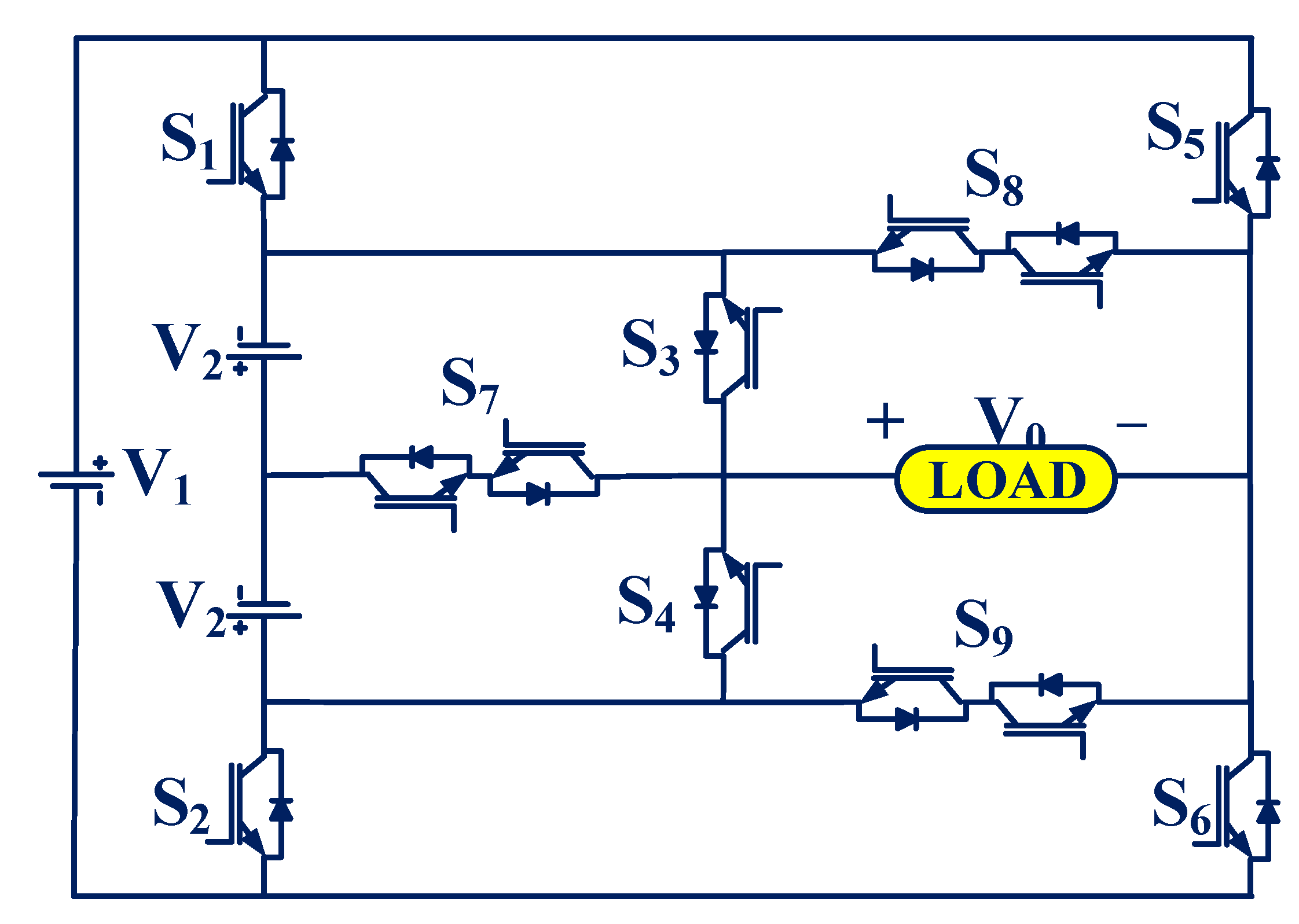
2. Proposed Structure

The proposed 11-level topology is depicted in Figure 1. Observably, the structure comprises six unidirectional switches and three bidirectional switches, requiring 12 IGBT components. A pair of bidirectional switches S8 and S9 are redundant, with these switches being used exclusively under faulty states. The structure utilizes three DC sources with per unit magnitudes of 0.5, 1, and 1, respectively. The structure can generate an 11-level output voltage waveform, with five levels each of positive and negative polarity, respectively, and a zero level. The switching strategy under healthy operation is described in Table 1, and the corresponding conduction diagram is presented in Figure 2. The ratio of the magnitude of the dc sources is as V2 = Vdc and V1 = 0.5Vdc. The total standing voltage (TSV) of the structure is 20Vdc, with the per-unit TSV having a magnitude of 20/2.5 = 8Vdc.

3. Fault-Tolerant Strategy

The modulation scheme must be reconfigured after an open-circuit fault is detected on any of the switches to sustain operation with acceptable output power quality and THD. The strategy for faults across individual switches is given in Table 2. The open-circuit fault can result in a reduced output power rating due to the loss of the peak level ±5Vdc in particular cases.
The blocking voltages of the switches are given as
S 1 = S 2 = 2.5 V d c
S 3 = S 4 = 2 V d c
S 5 = S 6 = 0.5 V d c
S 7 = 2 V d c
S 8 = S 9 = 3 V d c
The total TSV (total standing voltage) of the structure calculated as the sum of individual maximum blocking voltages is obtained as 18Vdc, with the per-unit TSV having a magnitude of 18/2.5 = 7.2Vdc. The switch voltage stresses do not increase post-fault and remain at their healthy condition or lower values.

Modulation Strategy

Implementing a low-frequency modulation technique effectively reduces voltage transients, snubber requirements, switching losses and has a positive effect on the reliability of the inverter [33]. Selective harmonic elimination (SHE-PWM) and nearest level control (NLC-PWM) are two techniques based on low frequency modulation. SHE is better at reducing the filter size by mitigating the lower order harmonics, but it requires solving complex transcendental equations which is computationally intensive. Moreover, the closed-loop implementation of NLC-PWM is simpler. This work uses NLC-PWM in light of the above issues. The switching angles θi [34,35] are calculated using:
θ i = M a s i n 1 ( 2 i 1 N 1 )
where MI stands for the modulation index with i = 1,2, …(N − 1)/2 (N = number of levels). The modulation index MI is equal to
M a   =   V r e f V 0  
Post-fault, modulation is reconfigured to generate new switching angles to maintain the output power quality with reduced or inconsecutive levels.
  • Fault in S1 or S2 or S5 or S6
The generation of levels ±V1, ± (V1 + V2), ± (2V2 + V1) cannot be sustained following a fault that occurs in this situation. The levels ±V2 and ±2V2 are produced post-fault. The respective conduction diagram under R-L load is shown in Figure 3. The load power rating is reduced as a result of the loss of the peak level. Modulation reconfiguration can give a satisfactory output voltage THD.
2.
Fault in S3 or S4
The levels ±V1, ±2V2, and ± (2V2 + V1) are lost in this case. The conduction diagram following this fault is given in Figure 4. Indeed, the fault leads to a similar reduction in load power rating.
3.
Fault IN S7
Following a fault in S7, the levels ±V1, ±2V2 cannot be further produced. However, a fault in this location does not affect the load power rating, as the peak level ±(2V2 + V1) is preserved. The conduction diagram for this scenario is illustrated in Figure 5.

4. Reliability Assessment

A reliability assessment is instrumental in evaluating the robustness of a circuit towards environmental stresses and gradual degradation. It is instrumental in predicting the expected lifespan of the inverter.

4.1. Component Failure Rate Evaluation

The failure rates of various components are influenced by numerous factors, such as voltage stress, thermal behavior, environment, as described in MIL-HDBK-217F [36]. The failure rate of a semiconductor switch is derived as:
λ s = λ b × π T × π A × π R × π S × π Q × π E
where the base failure rate λb is given as 0.00074. The thermal parameter πT is given by:
π T = exp ( 2114 ( 1 T J + 273 1 298 ) )
where TJ is the junction temperature of the device. The application factor πA corresponds to switching and is considered as 0.7. The power rating factor πR is given as
π R = P r ( 0.37 )
where Pr is the power rating of the switch. The voltage stress factor πS is given using
π R = 0 . 45   ×   exp   ( 3.1 × V S )
where VS = VCE (applied collector to emitter voltage)/VCEO (rated collector to emitter voltage with base open). The quality factor πQ is taken as unity for JANTX specifications. The environment factor (πE) is considered as benign ground environment with a value of unity.
1.
Thermal Power Loss
The non-ideal behavior of switches is manifested in the form of their conduction losses and switching losses. It, in turn, elevates the junction temperature of the device, resulting in decreased reliability and efficiency. The total conduction loss in an IGBT diode module in a fundamental period can be evaluated using Equation (12).
P c   = k = 1 N sw 1 2 π 0 2 π ( V sw i ( t ) + R s i β ( t ) ) dt + k = 1 N D 1 2 π 0 2 π ( V D i ( t ) + R D i 2 ( t ) ) dt
In the preceding expression, Vsw represents the ON-state switch voltage drop, Rs stands for the ON-state switch resistance; similar terms are denoted for the diode D. The module current is given by i(t). Further, the switching losses in the module can be computed by the following equations:
P s   = [ k = 1 Ns ( N ON k E ON k + N OFF k E OFF k )   ] × f
Here, N ON k and E ON k are taken as the number of transitions to OFF states and the associated energy loss, respectively, for the kth device, with the second term for ON transitions. The fundamental frequency is being denoted by f. The total thermal losses as an algebraic sum of the average conduction and switching losses is given by:
P loss   = P c + P s
The Foster thermal model was compiled in the PLECS environment. Figure 6 and Figure 7, respectively, denote the thermal description of the IGBT module IKW20N60H3 implemented. Heat sinks with reduced thermal resistances are not added. To simulate a worst-case scenario, the junction-to-ambient thermal resistance of the IGBT module itself is implemented for analysis. Following the thermal model, the π R and π T values are obtained.

4.2. Reliability Evaluation

The different failure rate parameters, and hence the failure rates of the various switches, are computed and are described in Table 3. The reliability function of the inverter under any switch open-circuit faults is evaluated using the following result:
R ( t ) = ( e λ 1 t ) 2 ( e λ 2 t ) 2 ( e λ 3 t ) 2 ( e λ 4 t ) 2 + 2 ( 1 e λ 1 t ) ( e λ 2 t ) 2 ( e λ 3 t ) 2 ( e λ 4 ) 2 + 2 ( 1 e λ 2 t ) ( e λ 1 t ) 2 ( e λ 3 t ) 2 ( e λ 4 t ) 2 + 2 ( 1 e λ 3 t ) ( e λ 1 t ) 2 ( e λ 2 t ) 2 ( e λ 4 t ) 2 + ( 1 e λ 4 t ) ( e λ 1 t ) 2 ( e λ 2 t ) 2 ( e λ 3 t ) 2  
The first term in the expression is for the healthy operation of the topology. The second term is for the case of post-fault in either of S1/S2. The third term of the equation represents conditions after a fault in S3/S4. Similarly, the third term of the equation represents a fault in one of S5/S6. The equation’s fourth term represents a fault in S7. In a situation where there is no fault management, the reliability of the inverter is substantially suppressed, as predictable by Equation (16).
R ( t ) = ( e λ 1 t ) 2 ( e λ 2 t ) 2 ( e λ 3 t ) 2 ( e λ 4 t ) 2
The distinction of reliability between fault management and its lack thereof can be visualized in Figure 8.

5. Comparative Analysis

In this section, the proposed topology is assessed competitively concerning fault-tolerant MLIs mentioned the in recent literature. Multiple parameters for assessment include the number of DC sources, power semiconductor switches, and levels generated. The comparison can be visualized using Table 4. The proposed topology shows advantages in terms of per-unit level device utilization and component requirements with the additional benefit of improved reliability. The literature works compared with the proposed topology include [16,17,18,37,38,39,40,41]. While the DC source requirement in [18,39] are same as the proposed topology, still they can produce only seven level output voltage. The topologies presented in [17,38,40,41] utilizes two DC sources, but they can only produce a maximum level of 5, 5, 7, and 9 respctively. Moreover, although the switch requirement in [17,37,38,39,40] is less compared to proposed topology, the ouptut voltage levels generated are also quite a bit lower. Comparison with a CHB topology with DC sources ±Vdc, ±2Vdc, ±2Vdc is also included. The CHB topology exhibits only partial fault tolerance in terms of post-fault peak level availability and reduced performance in case of faults in multiple switches while requiring 12 active IGBTs compared to 8, as in the case of the proposed topology. Consider a three-CHB with DC sources ±Vdc, ±2Vdc, ±2Vdc. The proposed topology can continue to produce a five-level output of 0, ±2Vdc, ±4Vdc in the event of both S1-S2, both S5-S6, and even all four S1, S2, S5, and S6 simultaneous failure by employing the redundant switches S8 and S9, while the loss of four switches will catastrophically affect the performance of the CHB inverter. Moreover, only eight IGBTs are active in the proposed topology during healthy conditions, and the other four are redundant, which results in higher reliability than the three-CHB inverter comprising 12 active IGBTs.
Table 4. Comparative assessment.
TopologyNo. of Dc SourcesNo. of CapacitorsNo. of Power DiodesNo. of SwitchesFault Tolerant/ReliableNo. of Levels
Binary CHB (1-2-2)30012YES (partial)11
[16]40020YES5
[17]2028YES5
[37]1228YES5
[38]2008YES5
[18]30012YES7
[39]30010YES7
[40]2209YES7
[41]21012YES9
Proposed30012YES11

6. Fault Detection

The proposed fault detection technique involves the acquisition of the mean load voltage and Root Mean Square (RMS) load voltage supplied by the MLI. The detection problem is a Multiclass Classification problem in machine learning, with fault location as the output and mean and RMS voltages as inputs. Various supervised learning classification algorithms have been developed, namely expert systems, linear regression, artificial neural networks (ANNs), a support vector machine (SVM), k-nearest neighbour (KNN), fuzzy logic, and decision trees (DTs). This work implements a decision tree model for the classification problem. DTs are one of the most versatile and popular models which can perform both classification and regression. A decision tree is in the structure of a tree, where each feature is represented as a node. A decision rule is represented as a branch (link), and each leaf classifies the output. The structure of a DT is depicted in Figure 9. The basic principle involves asking a series of true/false questions or decisions. Data are further categorized across every step. Each branch corresponds to a result of the test. Each leaf node assigns a classification of the output. DTs often mimic the human thinking flow, making them simple to understand and they help one in interpreting the implications of the data. The three steps performed are dataset preparation, training, and testing.
Assuming training vectors x i R n , i = 1 , l with a label vector y R l , the functioning of a decision tree involves recursively partitioning the features such that identically labelled or similar target outputs are aggregated together. Consider the data composed of Nm samples at node m and symbolised by Qm. A split θ = ( j , t m ) with j and tm as the feature and partition, respectively, partitions the data into the subsets Q m l e f t ( θ ) and Q m r i g h t ( θ ).
Q m l e f t ( θ ) = { ( x , y ) | x j t m }
Q m r i g h t ( θ ) = Q m / Q m l e f t ( θ )
The obtained candidate split is verified by its quality using a loss function H(),
G ( Q m , θ ) = N m l e f t N m H ( Q m l e f t ( θ ) ) + N m r i g h t N m H ( Q m r i g h t ( θ ) )
The impurity minimisation is performed by the following parameter:
θ * = a r g m i n θ G ( Q m , θ )
Recursion is performed for the subsets Q m l e f t ( θ * ) and Q m r i g h t ( θ * ) until the maximum allowable depth is achieved that is N m < m i n s a m p l e s or N m = 1 . For a classification application implementing 0…(K − 1) outputs for node m, assume that the proportions of class k outputs in node m given by
p m k = 1 / N m y Q m I ( y = k )
Then, the loss function corresponding to the Gini classification index is given by
H ( Q m ) k p k m ( 1 p m k )

6.1. Dataset Preparation

The mean and RMS values are acquired and are used as input to the model. Multiple inputs are obtained by varying the DC source voltages by 0%, ±1%, ±2%, ±5%, and ±10% to account for variations in load and dynamic behavior. Moreover, the above procedure is repeated for modulation indexes of 1, 0.9, 0.8, 0.7, 0.6, and 0.5. Distinct values across these parameters are obtained for fault in all seven switches and healthy operation. This gives a total of 432 input datasets, of which 75% are used for training the model. Selected sample datasets are displayed in Table 5 for S3 fault conditions. A plot of the total dataset obtained is shown in Figure 10. Classification 1 to 7 is used for respective faults in switches, with ‘0′ for no fault.

6.2. Training

The training was implemented on a ColabTM computational environment using the Python Scikit-learn library. Gini index classification was used as a metric. The importance of the features can be visualized in Figure 11. Observably, the mean voltage is a more important feature than the RMS values. The obtained decision tree structure is shown in Figure 12. The tree has 39 nodes and 38 branches with eight leaf nodes determining the fault location as the output.

6.3. Testing and Results

After training, testing was carried out to verify the performance of the prediction model. The Confusion matrix obtained post-training is given as:
[ 13 0 0 0 0 0 0 0 0 11 0 0 0 0 0 0 0 0 12 0 0 0 0 0 0 0 1 8 0 0 0 0 0 0 0 0 16 0 0 0 0 0 0 0 0 15 0 0 0 0 0 0 0 0 16 0 0 0 0 0 0 0 0 15 ]
The diagonal values are the correct predictions, and the non-diagonal elements are false positives and false negatives. As a result, the testing accuracy as a ratio of the number of correct predictions and total predictions was approximately 98.14%. An error of 1.86% is within satisfactory ranges for load and modulation index variation. Thus, the model can predict open-circuit fault locations with acceptable accuracy and low computational and hardware requirements.
The trained classification model was implemented in the MATLAB-Simulink environment for fault detection on the inverter model. The obtained simulation results are given in Figure 13. The simulation results indicate that the fault is detected within one fundamental period.
The method can also be expanded for multiple switch faults. The advantages of the given method include the requirement of only two measured signals, mean and RMS voltage, from the inverter, thus requiring minimal additional sensor and signal processing hardware requirements. Thus, the proposed method can work with minimal cost and complexity.

7. Results and Discussion

7.1. Simulation Results

The operation of the proposed topology was verified in the MATLAB-SimulinkTM R2016b environment on an Intel® CoreTM i5-3210M 2.50 GHz platform. The simulation parameters are listed in Table 6. Results under both normal and faulty operation are presented with the execution of the NLC-PWM modulation control. The load voltage and load current waveform and their respective harmonic profiles are given in Figure 14. The load voltage, load current, and the switch current waveforms in the scenario of S1/S2 or S5/S6 fault are shown in Figure 15. Similarly, the corresponding waveforms for faults in S3/S4 and S7 are shown in Figure 16 and Figure 17, respectively.

7.2. Experimental Verification

The operation of the proposed topology was verified through a hardware prototype depicted in Figure 18 using NLC (nearest level control) at 50 Hz fundamental frequency with Table 7 parameters. IGBTs IGB20N60H3 were used as switches. TMS320F28335 was used as the controller while TLP250H gate drivers were implemented. The output waveforms were displayed in a Yokogawa DL1640 oscilloscope. A total input DC source voltage of 50 V with V1 = 10 V and V2 = 20 V was fed to the module. An EN50160 power analyzer was used to determine the harmonic distortion in the load voltage waveforms. A load of 20 Ω + 50 mH was connected at the output. The output waveforms for S1 open-circuit fault for modulation indexes MI = 1 and MI = 0.7 are given in Figure 19. Similarly, the output waveforms for S3 fault and S7 fault are given in Figure 20 and Figure 21, respectively. The fault-tolerant operation was successful, even with the variation of MI. Moreover, the waveform distortion arising from the open-circuit fault was corrected in one fundamental period. The harmonic spectrum of load voltages for healthy conditions, S1 post- fault, S3 post-fault, and S7 post-fault, are given in Figure 22. Observably, the THD is higher post-fault but is at acceptable values and can be supplied to critical loads with low filter requirements.

8. Conclusions

In this paper, an asymmetric multilevel inverter topology is introduced. The fault tolerance of the proposed topology against switch open-circuit faults due to gating failure is verified through simulation results. Reliability analysis of the topology is presented to illustrate the advantage of fault tolerance. The topology is compared against previous works in terms of device count and other parameters to demonstrate its superiority. Additionally, a fault detection strategy using the supervised machine learning technique decision trees is put forth. The fault localization model inputs the load mean voltage and its RMS as diagnostic variables and outputs the fault location. The testing results demonstrate that the classification model successfully detects the fault location with an accuracy of 0.981481. Therefore, the fault detection strategy can be expanded to a real-time system in the future with low computational requirements and minimal additional hardware.

Author Contributions

Conceptualization, M.F. and A.S.; Formal analysis, M.F., M.M. and M.A.Z.; Funding acquisition, M.T. (Mohd Tariq), B.A. and A.A.; Investigation, M.F. and M.T. (Mohd Tariq); Methodology, M.F. and A.S.; Project administration, M.T. (Mohd Tariq); Supervision, A.S.; Validation, M.R.H. and M.T. (Mohammad Tayyab); Writing—original draft, M.F. and M.M.; Writing—review & editing, M.T. (Mohd Tariq), A.S., M.A.Z., K.S., B.A. and A.A. All authors have read and agreed to the published version of the manuscript.

Funding

This research was funded in part by Taif University Researchers Supporting Project Number (TURSP-2020/121), Taif University, Taif, Saudi Arabia and in part by the collaborative research grant scheme (CRGS) project granted by the Capability Systems Centre, UNSW-Canberra at ADFA to the Hardware-In-the-Loop (HIL) Lab, Department of Electrical Engineering, Aligarh Muslim University, India, with project number CRGS/MOHD TARIQ/01.

Institutional Review Board Statement

Not applicable.

Informed Consent Statement

Not applicable.

Acknowledgments

The authors also acknowledge the support provided by the Hardware-In-the-Loop (HIL) Lab and Non-Conventional Energy (NCE) Lab, Department of Electrical Engineering, Aligarh Muslim University, India.

Conflicts of Interest

The authors declare no conflict of interest.

References

  1. Zand, M.; Nasab, M.A.; Hatami, A.; Kargar, M.; Chamorro, H.R. Using Adaptive Fuzzy Logic for Intelligent Energy Management in Hybrid Vehicles. In Proceedings of the 2020 28th Iranian Conference on Electrical Engineering (ICEE), Tabriz, Iran, 4–6 August 2020; pp. 1–7. [Google Scholar] [CrossRef]
  2. Ahmadi-Nezamabad, H.; Zand, M.; Alizadeh, A.; Vosoogh, M.; Nojavan, S. Multi-objective optimization based robust scheduling of electric vehicles aggregator. Sustain. Cities Soc. 2019, 47, 101494. [Google Scholar] [CrossRef]
  3. Bana, P.R.; Panda, K.P.; Naayagi, R.T.; Siano, P.; Panda, G. Recently developed reduced switch multilevel inverter for renewable energy integration and drives application: Topologies, comprehensive analysis and comparative evaluation. IEEE Access 2019, 7, 54888–54909. [Google Scholar] [CrossRef]
  4. Arash, R.; Mahmood, J.; Mahyar, A.; Mohammad, Z. Three-phase amplitude adaptive notch filter control design of DSTATCOM under unbalanced/distorted utility voltage conditions. Intell. Fuzzy Syst. 2019, 37, 847–865. [Google Scholar]
  5. Dahidah, M.S.A.; Konstantinou, G.; Agelidis, V.G. A review of multilevel selective harmonic elimination PWM: Formulations, solving algorithms, implementation and applications. IEEE Trans. Power Electron. 2014, 30, 4091–4106. [Google Scholar] [CrossRef]
  6. Rodríguez, J.; Lai, J.S.; Peng, F.Z. Multilevel inverters: A survey of topologies, controls, and applications. IEEE Trans. Ind. Electron. 2002, 49, 724–738. [Google Scholar] [CrossRef] [Green Version]
  7. Dewangan, N.K.; Prakash, T.; Tandekar, J.K.; Gupta, K.K. Open-circuit fault-tolerance in multilevel inverters with reduced component count. Electr. Eng. 2019, 102, 409–419. [Google Scholar] [CrossRef]
  8. Cao, W.; Mecrow, B.C.; Atkinson, G.J.; Bennett, J.W.; Atkinson, D.J. Overview of electric motor technologies used for more electric aircraft (MEA). IEEE Trans. Ind. Electron. 2012, 59, 3523–3531. [Google Scholar]
  9. Kirtley, J.L.; Banerjee, A.; Englebretson, S. Motors for ship propulsion. Proc. IEEE 2015, 103, 2320–2332. [Google Scholar] [CrossRef]
  10. Kaboli, S.; Oraee, H. Reliability in Power Electronics and Electrical Machines: Industrial Applications and Performance Models: Industrial Applications and Performance Models; IGI Global: Hershey, PA, USA, 2016. [Google Scholar]
  11. Sathik, M.H.M.; Prasanth, S.; Sasongko, F.; Pou, J. Lifetime estimation of off-the-shelf aerospace power converters. IEEE Aerosp. Electron. Syst. Mag. 2018, 33, 26–38. [Google Scholar] [CrossRef]
  12. Formica, T.J.; Khan, H.A.; Pecht, M.G. The Effect of inverter failures on the return on investment of solar photovoltaic systems. IEEE Access 2017, 5, 21336–21343. [Google Scholar] [CrossRef]
  13. Cordeiro, A.; Palma, J.; Maia, J.; Resende, M. Fault-Tolerant Design of a Classical Voltage-Source Inverter Using Z-Source and Standby Redundancy. In Proceedings of the International Conference on Electrical Power Quality and Utilisation, EPQU, Lisbon, Portugal, 17–19 October 2011; pp. 648–653. [Google Scholar]
  14. Chen, A.; Hu, L.; Chen, L.; Deng, Y.; He, X.; Member, S. A multilevel converter topology with fault-tolerant ability. IEEE Trans. Power Electros. 2005, 20, 405–415. [Google Scholar] [CrossRef]
  15. Chen, Y.; Li, Z.; Zhao, S.; Wei, X.; Kang, Y. Design and implementation of a modular multilevel converter with hierarchical redundancy ability for electric ship MVDC system. IEEE J. Emerg. Sel. Top. Power Electron. 2017, 5, 189–202. [Google Scholar] [CrossRef]
  16. Nicolas-Apruzzese, J.; Busquets-Monge, S.; Bordonau, J.; Alepuz, S.; Calle-Prado, A. Analysis of the fault-tolerance capacity of the multilevel active-clamped converter. IEEE Trans. Ind. Electron. 2013, 60, 4773–4783. [Google Scholar] [CrossRef]
  17. Madhukar Rao, A.; Sivakumar, K. A fault-tolerant single-phase five-level inverter for grid-independent PV systems. IEEE Trans. Ind. Electron. 2015, 62, 7569–7577. [Google Scholar]
  18. Aguayo-Alquicira, J.; Vásquez-Libreros, I.; De Léon-Aldaco, S.E.; Ponce-Silva, M.; Lozoya-Ponce, R.E.; Flores-Rodríguez, E.; García-Morales, J.; Reyes-Severiano, Y.; Carrillo-Santos, L.M.; Marín-Reyes, M.; et al. Reconfiguration strategy for fault tolerance in a cascaded multilevel inverter using a Z-source converter. Electronics 2021, 10, 574. [Google Scholar] [CrossRef]
  19. Brando, G.; Dannier, A.; del Pizzo, A.; Rizzo, R. Quick Identification Technique of Fault Conditions in Cascaded H-Bridge Multilevel Converters. In Proceedings of the International Aegean Conference on Electrical Machines and Power Electronics and Electromotion ACEMP’07 and Electromotion’07 Joint Conference, Istanbul, Turkey, 2–4 September 2007; pp. 491–497. [Google Scholar]
  20. Lezana, P.; Aguilera, R.; Rodríguez, J. Fault detection on multicell converter based on output voltage frequency analysis. IEEE Trans. Ind. Electron. 2009, 56, 2275–2283. [Google Scholar] [CrossRef] [Green Version]
  21. Pires, V.F.; Foito, D.; Sousa, D.M.; Martins, J.F. Fault Detection on Multilevel Power Converter Based on Mass Center of the Voltage Pattern. In Proceedings of the International Conference on Power Engineering, Energy and Electrical Drives, Istanbul, Turkey, 13–17 May 2013; pp. 576–581. [Google Scholar]
  22. Shao, S.; Wheeler, P.W.; Clare, J.C.; Watson, A.J. Fault detection for modular multilevel converters based on sliding mode observer. IEEE Trans. Power Electron. 2013, 28, 4867–4872. [Google Scholar] [CrossRef] [Green Version]
  23. Anand, A.; Raj, N.; George, S.; Jagadanand, G. Open Switch Fault Detection in Cascaded H-Bridge Multilevel Inverter Using Normalised Mean Voltages. In Proceedings of the 2016 IEEE 6th International Conference on Power Systems (ICPS 2016), New Delhi, India, 4–6 March 2016. [Google Scholar]
  24. Anand, A.; Vinayak, B.A.; Raj, N.; Jagadanand, G.; George, S. A generalized switch fault diagnosis for cascaded h-bridge multilevel inverters using mean voltage prediction. IEEE Trans. Ind. Appl. 2020, 56, 1563–1574. [Google Scholar] [CrossRef]
  25. Raj, N.; Kale, T.; Anand, A.; Jagadanand, G.; George, S. Switch fault detection and diagnosis in space vector modulated cascaded H-bridge multilevel inverter. Int. J. Electron. 2018, 105, 1977–1992. [Google Scholar] [CrossRef]
  26. Zhao, S.; Blaabjerg, F.; Wang, H. An overview of artificial intelligence applications for power electronics. IEEE Trans. Power Electron. 2021, 36, 4633–4658. [Google Scholar] [CrossRef]
  27. Tolbert, S.K.L.M. Fault diagnosis and reconfiguration for multilevel inverter drive using AI-based techniques. IEEE Trans. Ind. Electron. 2007, 54, 2954–2968. [Google Scholar]
  28. Wang, T.; Qi, J.; Xu, H.; Wang, Y.; Liu, L.; Gao, D. Fault diagnosis method based on FFT-RPCA-SVM for Cascaded-Multilevel Inverter. ISA Trans. 2016, 60, 156–163. [Google Scholar] [CrossRef] [PubMed]
  29. Zand, M.; Nasab, M.A.; Neghabi, O.; Khalili, M.; Goli, A. Fault Locating Transmission Lines with Thyristor-Controlled Series Capacitors By Fuzzy Logic Method. In Proceedings of the 2020 14th International Conference on Protection and Automation of Power Systems (IPAPS), Tehran, Iran, 31 December–1 January 2020; pp. 62–70. [Google Scholar] [CrossRef]
  30. Raj, N.; George, S.; Jagadanand, G. Open Transistor Fault Detection in Asymmetric Multilevel Inverter. In Proceedings of the 2015 IEEE International Conference on Signal Processing, Informatics, Communication and Energy Systems, SPICES 2015, Kozhikode, India, 19–21 February 2015. [Google Scholar]
  31. Raj, N.; Jagadanand, G.; George, S. Fault detection and diagnosis in asymmetric multilevel inverter using artificial neural network. Int. J. Electron. 2018, 105, 559–571. [Google Scholar] [CrossRef]
  32. Omer, P.; Kumar, J.; Surjan, B.S. A review on reduced switch count multilevel inverter topologies. IEEE Access 2020, 8, 22281–22302. [Google Scholar] [CrossRef]
  33. Sathik, M.J.; Prabaharan, N.; Ibrahim, S.A.A.; Vijaykumar, K.; Blaabjerg, F. A new generalized switched diode multilevel inverter topology with reduced switch count and voltage on switches. Int. J. Circuit Theory Appl. 2020, 48, 619–637. [Google Scholar] [CrossRef]
  34. Nguyen, M.H.; Kwak, S. Nearest-level control method with improved output quality for modular multilevel converters. IEEE Access 2020, 8, 110237–110250. [Google Scholar] [CrossRef]
  35. Hu, P.; Jiang, D. A level-increased nearest level modulation method for modular multilevel converters. IEEE Trans. Power Electron. 2015, 30, 1836–1842. [Google Scholar] [CrossRef]
  36. MIL-HDBK-217 F Reliability Prediction Electronic. Available online: http://everyspec.com/MIL-HDBK/MIL-HDBK-0200-0299/MIL-HDBK-217F_14591/ (accessed on 1 October 2020).
  37. Jalhotra, M.; Kumar, L.; Gautam, S.P.; Gupta, S. Development of fault-tolerant MLI topology. IET Power Electron. 2018, 11, 1416–1424. [Google Scholar] [CrossRef]
  38. Dewangan, N.K.; Gupta, S.; Gupta, K.K. Approach to synthesis of fault tolerant reduced device count multilevel inverters (FT RDC MLIs). IET Power Electron. 2019, 12, 476–482. [Google Scholar] [CrossRef]
  39. Choupan, R.; Golshannavaz, S.; Nazarpour, D.; Barmala, M. A new structure for multilevel inverters with fault-tolerant capability against open circuit faults. Electr. Power Syst. Res. 2019, 168, 105–116. [Google Scholar] [CrossRef]
  40. Chappa, A.; Gupta, S.; Sahu, L.K.; Gupta, K.K. Resilient multilevel inverter topology with improved reliability. IET Power Electron. 2020, 13, 3384–3395. [Google Scholar] [CrossRef]
  41. Kumar, D.; Nema, R.K.; Gupta, S. Investigation of fault-tolerant capabilities of some recent multilevel inverter topologies. Int. J. Electron. 2021. [Google Scholar] [CrossRef]
Figure 1. Structure of proposed multilevel inverter topology.
Energies 14 04302 g001
Figure 2. Conduction states during healthy operation.
Energies 14 04302 g002
Figure 3. Bypassing of faulted S1 by body diode and following conduction states.
Energies 14 04302 g003
Figure 4. Bypassing of faulted S3 by body diode and following conduction states.
Energies 14 04302 g004
Figure 5. Faulted S7 and following conduction states.
Energies 14 04302 g005
Figure 6. IGBT thermal loss description conduction, turn-on and turn-off losses.
Energies 14 04302 g006
Figure 7. Diode thermal loss description, conduction and turn-off losses.
Energies 14 04302 g007
Figure 8. Reliability curve.
Energies 14 04302 g008
Figure 9. Structure of proposed multilevel inverter topology.
Energies 14 04302 g009
Figure 10. Dataset plot.
Energies 14 04302 g010
Figure 11. Feature importance.
Energies 14 04302 g011
Figure 12. Obtained decision tree.
Energies 14 04302 g012
Figure 13. Fault detection simulation results. (a) S1 fault (b) S3 fault (c) S5 fault (d) S7 fault.
Energies 14 04302 g013aEnergies 14 04302 g013b
Figure 14. Load voltage and current simulation waveforms under healthy operation. (a) voltage waveform (b) current waveform.
Energies 14 04302 g014
Figure 15. Simulation voltage and current waveforms under S1 fault.
Energies 14 04302 g015
Figure 16. Simulation voltage and current waveforms under S3 fault.
Energies 14 04302 g016
Figure 17. Simulation voltage and current waveforms under S7 fault.
Energies 14 04302 g017
Figure 18. Experimental setup.
Energies 14 04302 g018
Figure 19. Experimental voltage and current waveforms under S1 fault.
Energies 14 04302 g019
Figure 20. Experimental voltage and current waveforms under S3 fault.
Energies 14 04302 g020
Figure 21. Experimental voltage and current waveforms under S7 fault.
Energies 14 04302 g021
Figure 22. Harmonic spectra under (a) healthy condition (b) S1 fault (c) S3 fault (d) S7 fault.
Energies 14 04302 g022aEnergies 14 04302 g022b
Table 1. Switching states for the proposed topology.
S1S2S3S4S5S6S7V0
10101000
1010010V1
1000101V2
1000011V1 + V2
10011002V2
1001010V1 + 2V2
01010100
0101100−V1
0100011−V2
0100101−(V1 + V2)
0110010−2V2
0110100−(V1 + 2V2)
Table 2. Fault management strategy.
Faulty SwitchesLevels Preserved Post-FaultPeak Levels Remaining
S1 or S2±V2, ± 2V2, zero±2V2
S3 or S4±V2, ±(V1 + V2), zero±(V2 + V1)
S5 or S6±V2, ± 2V2, zero±2V2
S7±V1, ±2V2, ±(V1 + 2V2), zero± (V1 + 2V2)
Table 3. Device failure rate parameters.
SwitchesJunction Temp. (°C)ΠTPower Loss (W)ΠRVsΠSλs
S1/S2248.7320.825.331.850.41 0.21λ1 = 0.00421
S3/S4190.85212.633. 901.650.330.16λ2 = 0.00172
S5/S623018.014.901.800.080.11λ3 = 0.00184
S7119.2725.503.391.570.160.11λ4 = 0.000492
Table 5. Sample dataset features.
Mean Load VoltageRMS Load VoltageFault in Switch
−45.2079.291
66.56116.112
6.014122.003
−4.7287.694
16.65108.495
−13.7599.346
−0.00014137.927
−3 × 10⁻⁶−3 × 10−60 (NO Fault)
Table 6. Simulation and reliability model parameters.
IGBT-diode moduleIGB20N60H3
Dc source voltages V1, V250 V, 100 V
Load20 Ω, 40 mH
Power960 W
ModulationNLC
Fundamental Frequency50 Hz
Heat sink addedNO
Initial temperature and ambient298 K
Table 7. Experimental parameters.
IGBT-diode moduleIGB20N60H3
Dc source voltages V1, V210 V, 20 V
Load20 Ω, 50 mH
Power 125 W
ModulationNLC
Fundamental Frequency50 Hz
ControllerTMS320F28335
Gate DriversTLP250H
Publisher’s Note: MDPI stays neutral with regard to jurisdictional claims in published maps and institutional affiliations.

