1. Introduction
Rapid development of body-worn sensors systems integrated on a chip imposes a significant demand on small and efficient power supply circuits. Batteries are avoided in these types of applications because of their relatively large size and limited life span. Among alternative energy sources such as photovoltaic cells [
1], vibration transducers [
2], or the thermoelectric generators (TEGs) [
3,
4,
5], the latter ones are widely used due to their small size, portability and suitability for on-body applications. TEGs exploit temperature gradient between the human skin and the ambient environment in practical situations. Small TEG size and low temperature difference (typically 1–2 °C) limit the upper voltage bound below 100 mV. Such a low voltage can be applied to slow circuits based on MOS transistors operating in the subthreshold region. However, many systems-on-chip implementing sophisticated functions require MOS transistors operating in the strong inversion region, which involves the use of supply voltages of around 1 V. Although boost converters can be used to raise voltages as low as 20–40 mV [
6,
7,
8,
9,
10,
11] to the required supply level, they also need a voltage within 1 V for efficient energy conversion. For this reason, an additional starter is used to allow “cold start” of the converter at low voltages. Such a circuit is turned on for a short time needed to start the converter, and then turned off once the converter supplies sufficient voltage to its own control circuits. In practical implementations of ULV boost converters, very significant difficulties are associated with realization of their starters.
Starter solutions designed to initialize the operation of on-chip boost converters are described in the literature [
7,
8,
9,
10,
12,
13,
14,
15,
16,
17]. The solutions can be classified into two major groups: starters based on classic ring oscillators using only transistors [
12,
16,
17], and starters based on oscillators with inductors or transformers [
7,
9,
10,
12,
13,
14]. In ring oscillators, each stage must have a gain greater than one in order to start and sustain oscillations. Satisfying this condition at very low supply voltages is very difficult, where all transistors have relatively low transconductance and drain-source resistance [
18,
19,
20,
21]. The lowest supply voltage reported for this type of starter is 60 mV [
13]. This level was achieved by applying a mechanism for technology corner detection and automatic reconfiguration of the ring oscillator to achieve almost optimal operating conditions. The ring oscillator using only transistors generates output voltages that are limited by the supply voltage, therefore, they need an additional multistage (in some solutions up to 40 stages [
13]) charge pump to obtain a sufficiently high voltage. As a result, ring-oscillator-based starters are fairly complicated and have a relatively low efficiency. On the other hand, they can be fully integrated on a chip.
Inductor or transformer-based starters support much lower supply voltages. In these circuits, a transformer or inductor acts as a load for a MOS transistor, allowing for voltage swing greater than the supply voltage and eliminating the inevitable voltage drop across the active load as in the case of a transistor-only ring oscillator. Consequently, they are capable of self-starting at supply voltages as low as 25–40 mV [
7,
9]. Moreover, an output voltage within 1 V can be achieved without additional charge-pump-based voltage multipliers owing to boosting voltage in a transformer or a LC resonant tank. In this regard, such starters are preferable over ones based on ring oscillators owing to their reliability, even with the supply voltages of only 25–40 mV. The disadvantage of these solutions is the need for inductors, which often have to be implemented as off-chip components to meet the high quality factor requirement.
In terms of the feasibility of reducing the startup voltage, the starters based on the Colpitts oscillator are particularly promising [
12,
14,
18,
19]. The paper [
19] gives an example implementation of a low-voltage Colpitts oscillator that operates even at 3.5 mV supply voltage. This circuit has indeed a very low inrush voltage but reveals a limitation of the output voltage swing. As a result, the circuit requires an additional multi-stage voltage multiplier to achieve a voltage close to 1 V.
This paper describes a low voltage starter based on an improved Colpitts oscillator featuring a high output voltage swing, which allows using only a few stages of a charge pump.
2. Ultra-Low-Voltage Oscillators
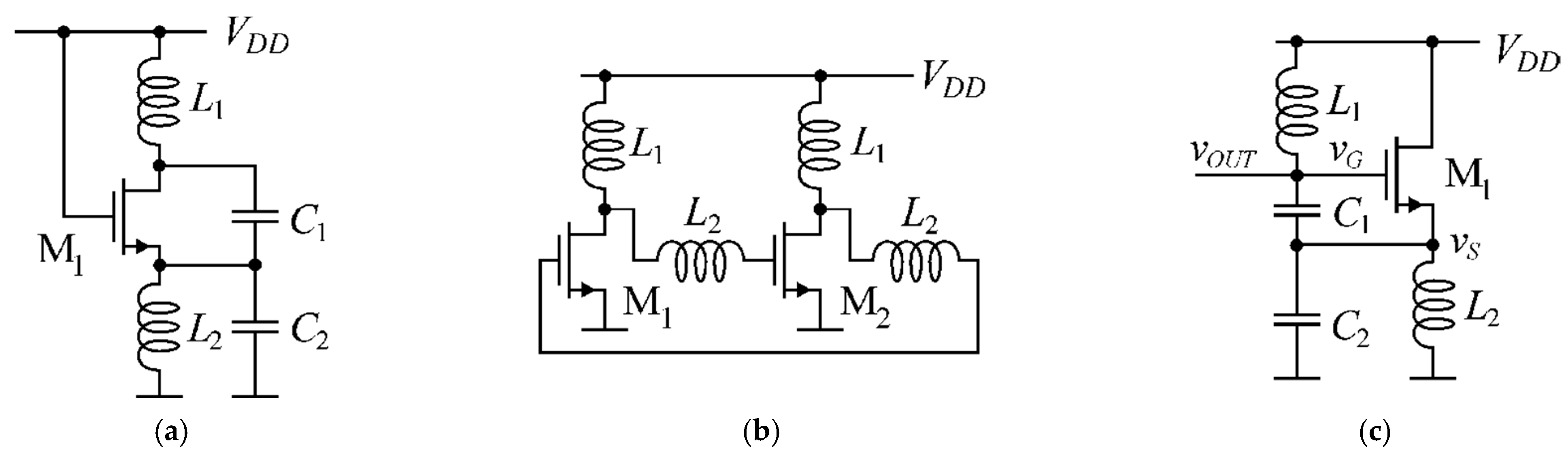
Three configurations of ULV oscillator potentially suitable as a boost converter starter are depicted in
Figure 1.
The oscillators in
Figure 1a,b are ULV solutions discussed in [
18,
19], referred to as enhanced swing Colpitts oscillator (ESCO) and inductive-load enhanced swing ring oscillator (ESILRO). The circuit in
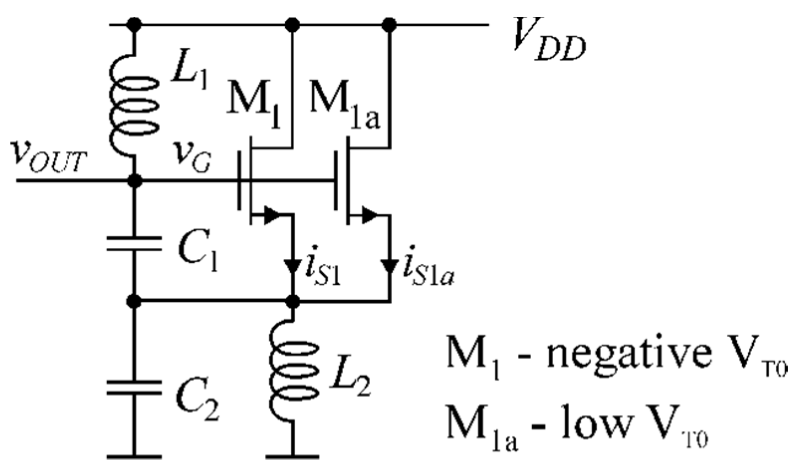
Figure 1c is a proposed high swing Colpitts oscillator (HSCO). The common feature of all the ULV circuits is the application of the full supply voltage (
VDD) to bias the transistor gate and drain. In this way, a sufficiently high intrinsic gain of the transistor can be achieved at a relatively low supply voltage. For this reason, two inductors are necessary to avoid voltage drop between the
VDD rail, drain and gate of the transistor. An unavoidable disadvantage of ESCO and ESILRO is limited voltage swing at the drains of the transistors. The reason for this effect is the pn junction between the drain and the substrate, which is forward biased during the negative halves of the generated periodic voltage waveform.
This undesirable effect is avoided in HSCO by connecting the resonant tank with the inductor
L1 to the transistor gate and design the feedback loop (
C1,
C2) so that the voltage scaling factor
vG/
vS is much larger than unity. Under such conditions, the voltage swing on the resonant tank is virtually unlimited. At the same time, voltage across the pn junction formed between the source and the substrate is highly reduced, which prevents it from forward bias. In the small-signal model of the circuit, shown in
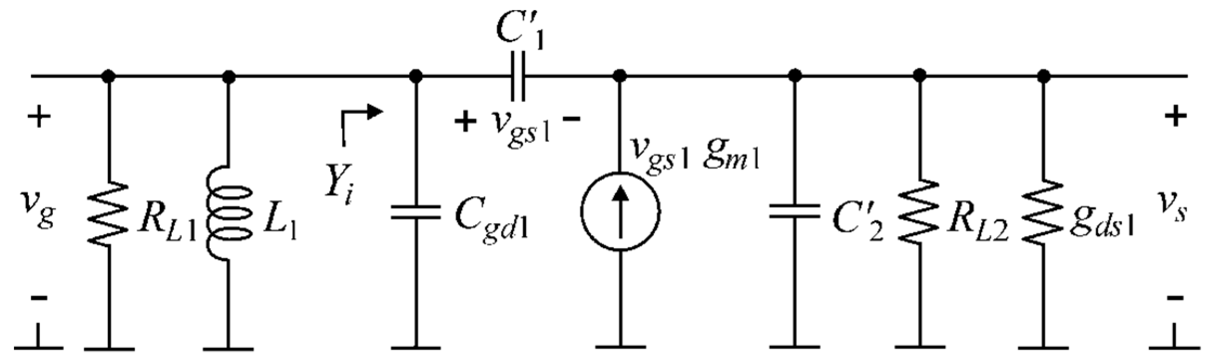
Figure 2, the biasing inductor
L2 is represented by its dynamic resistance
RL2 at oscillation frequency
ω0.
In
Figure 2, the transistor M
1, represented by
gm1 and
gds1, together with the capacitors
C′1,
C′2 and the dynamic resistance
RL2 form a circuit that implements the admittance
Yi with negative real part (conductance). The negative conductance allows compensation for the losses of inductor
L1, represented by
RL1. The real and imaginary parts of the admittance
Yi(
ω) seen from the gate of M
1 are
where:
C′1 =
C1 +
Cgs1,
C′2 =
C2 +
Csb1 − 1/(
ω2L2),
R0 = 1/(
gds1 + 1/
RL2). The negative real part of the admittance
Yi(
ω) can be obtained when the following condition is satisfied
For a transistor operating at low supply voltage, this condition also means that
C′2 >>
C′1, due to the fact that 1/
R0 >>
gm1. Therefore, further considerations are restricted to such a case. The
L1 inductor losses will be compensated and oscillations with frequency
ω0 will start if the following conditions are met
With the condition
C′2 >>
C′1, the Equation (1) can be simplified to
The simplified Equation (6) was derived under assumption that
gds1 >>
gm1 which is satisfied when M
1 operates at very low supply voltages. To satisfy the Equation (4), transconductance of M
1 must fulfill
The absolute minimum transconductance
gm1 can be achieved when both inductors are lossless (
RL1,
RL2 → ∞). In such a case, oscillations will start when the transconductance of M
1 meets the condition
It is worth noting that in theory by minimization of
C′1/
C′2 ratio an arbitrarily small value of
gm1 can be achieved, and thus an arbitrarily low supply voltage can be obtained. In practice the inductors are lossy, therefore
gm1 can be reduced by minimizing the last component of Equation (7) and by selecting the optimal value of the
C′2/
C′1 ratio. Reduction of the last component in Equation (7) requires that
Under the assumption that Equation (9) is fulfilled, the optimal value of the capacitance ratio is given as
and the minimum transconductance required to start the oscillations is
Note that according to Equation (9), it is advantageous to choose the highest possible oscillation frequency (ω0) and the largest capacitances C′1, C′2. Thus, in order to minimize the transconductance required to start oscillations in Equation (7), small inductances L1 and L2 and large capacitances C′1, C′2 are advantageous, which is also very beneficial for integration of the oscillator.
3. Minimum Supply Voltage Required to Start ULV Oscillators
Low supply voltage and high output swing are important criteria for choosing an oscillator as a starter for ULV boost converter. To identify which of the configurations shown in
Figure 1 is best suited as a starter, the minimum supply voltages of these circuits were determined and compared. In further considerations ESILRO is omitted due to the need for four inductors, which is difficult to integrate. N-channel MOS transistors with near-zero threshold voltage as well as negative threshold voltage are good candidates for implementing ULV oscillators because they provide relatively high drain current at supply voltages below a few tens of mV [
18,
19,
21]. Therefore, the minimum supply voltages of ESCO and HSCO were determined for the transistor operating in the weak and strong inversion regions.
For the sake of simplicity, in the compared oscillators it was assumed that both inductances as well as their losses are identical (
L1 =
L2,
GL1 =
GL2). According to the analysis presented in [
19], oscillations will start in ESCO if the following condition holds
where
where
gms1 and
gmd1 are the source and drain transconductances [
19,
20]. The ratio of these conductances for strong and weak inversion regions can be approximated [
19,
20] by
where
VT0 is the threshold voltage,
n is the slope factor of the current-voltage characteristic in the weak inversion region,
UT is the thermal voltage, and
VDS is the drain-source voltage.
The minimum supply voltage necessary to start oscillations in ESCO can be determined from Equations (12)–(15) for the strong and weak inversion regions, respectively [
19]
In HSCO, oscillations start when Equation (11) is satisfied. Based on this equation, the minimum ratio of the gate transconductance (
gm1) to the output conductance (
gds1) of the transistor can be determined as
where
GL1/
gds1 represents the ratio of
L1 losses, modeled by
GL1 = 1/
RL1, to the transistor output conductance. The ratio of the transistor transconductance to its output conductance for the strong and weak inversion regions can be defined [
19,
20] as
The minimum supply voltage for HSCO,
VDD,min, determined based on Equations (18)–(20), is for the strong and weak inversion regions, respectively
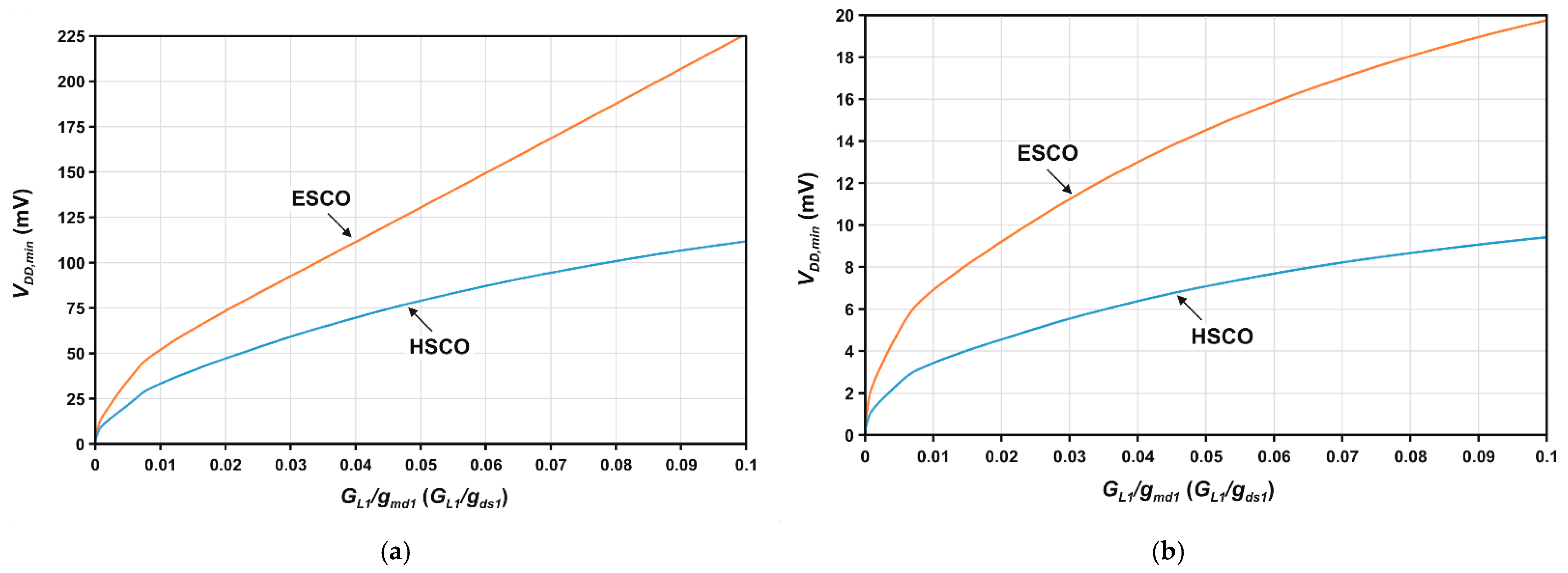
The comparison of the minimum supply voltage,
VDD,min, defined by Equations (16), (17), (21) and (22), for ESCO and HSCO is plotted in
Figure 3a,b, for the strong and weak inversion regions, respectively. The calculations for the strong inversion region are based on extracted values of
VT0 and
n for particular
VGS =
VDS =
VDD voltage values for a native n-channel MOS transistor (W/L = 2500 μm/1 μm) in X-FAB 180-nm CMOS technology. The plots for the weak inversion were made for
UT = 26 mV and similar values of the parameter
n.
The results in
Figure 3a,b show that HSCO requires significantly lower supply voltage compared to ESCO. This feature is particularly evident for high values of
GL1/
gds1, which corresponds to use of low quality factor inductors. The general Equations (16), (17), (21) and (22), defining the minimum startup voltage, were derived based on a simplified linear model. To provide more in-depth investigation of the considered oscillators properties, number of HSCO and ESCO oscillator designs using native n-channel MOS transistors with negative threshold voltage were prepared for a 180-nm X-FAB technology. For each oscillator design, the component parameters were optimized to obtain the minimum startup voltage,
VDD,min, for selected values of:
GL1/
gmd1 (
GL1/
gds1), inductances
L1 =
L2, and inductor quality factors
QL. A summary of the oscillators parameters is shown in
Table 1.
Based on the data from
Table 1, one can see that HSCO oscillator, compared to the ESCO, exhibits lower inrush voltage for similar values of
GL1/
gds1 and inductor quality factor
QL. For the variants
GL1/
gds1 = 0.001,
QL = 255, and
GL1/
gds1 = 0.005,
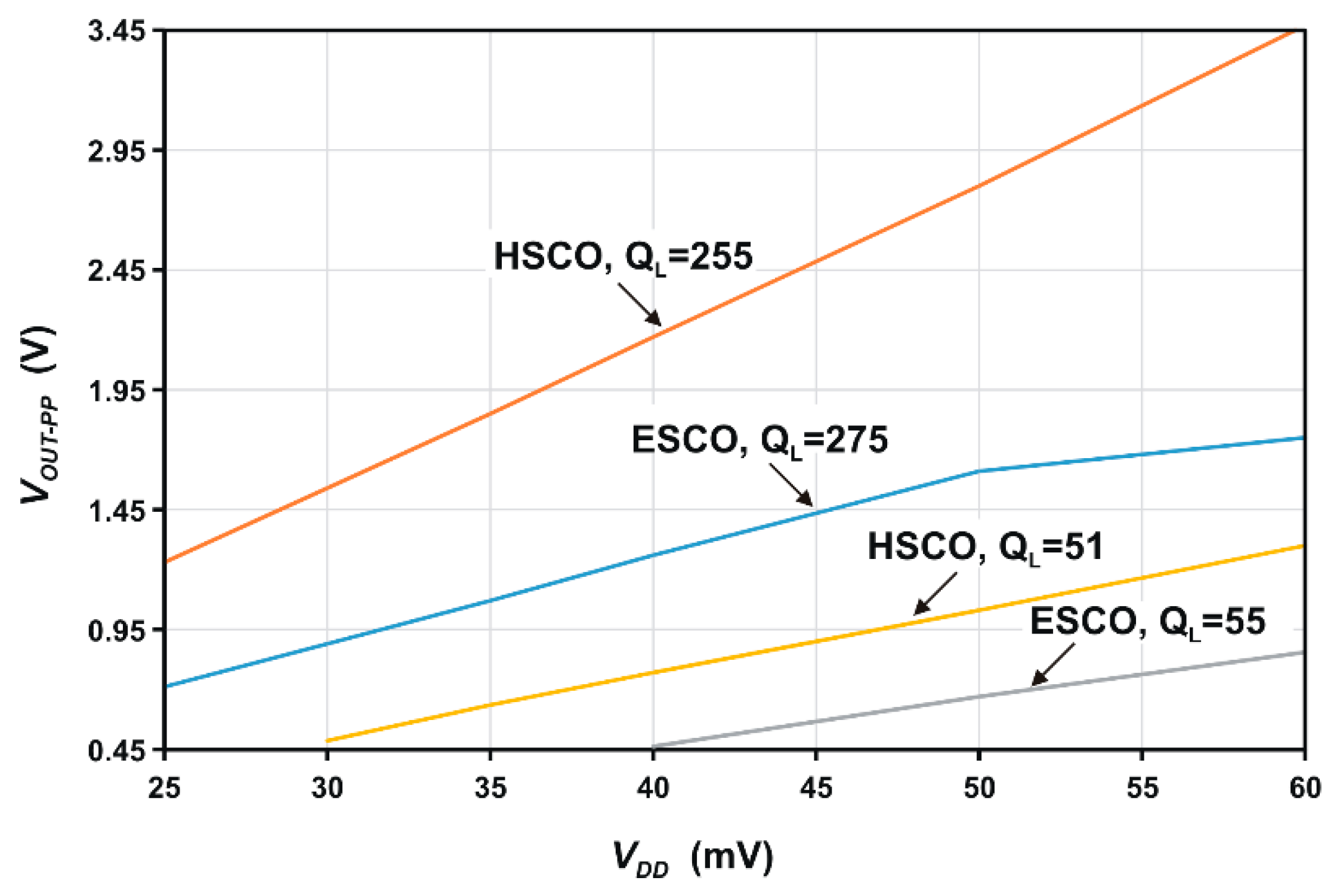
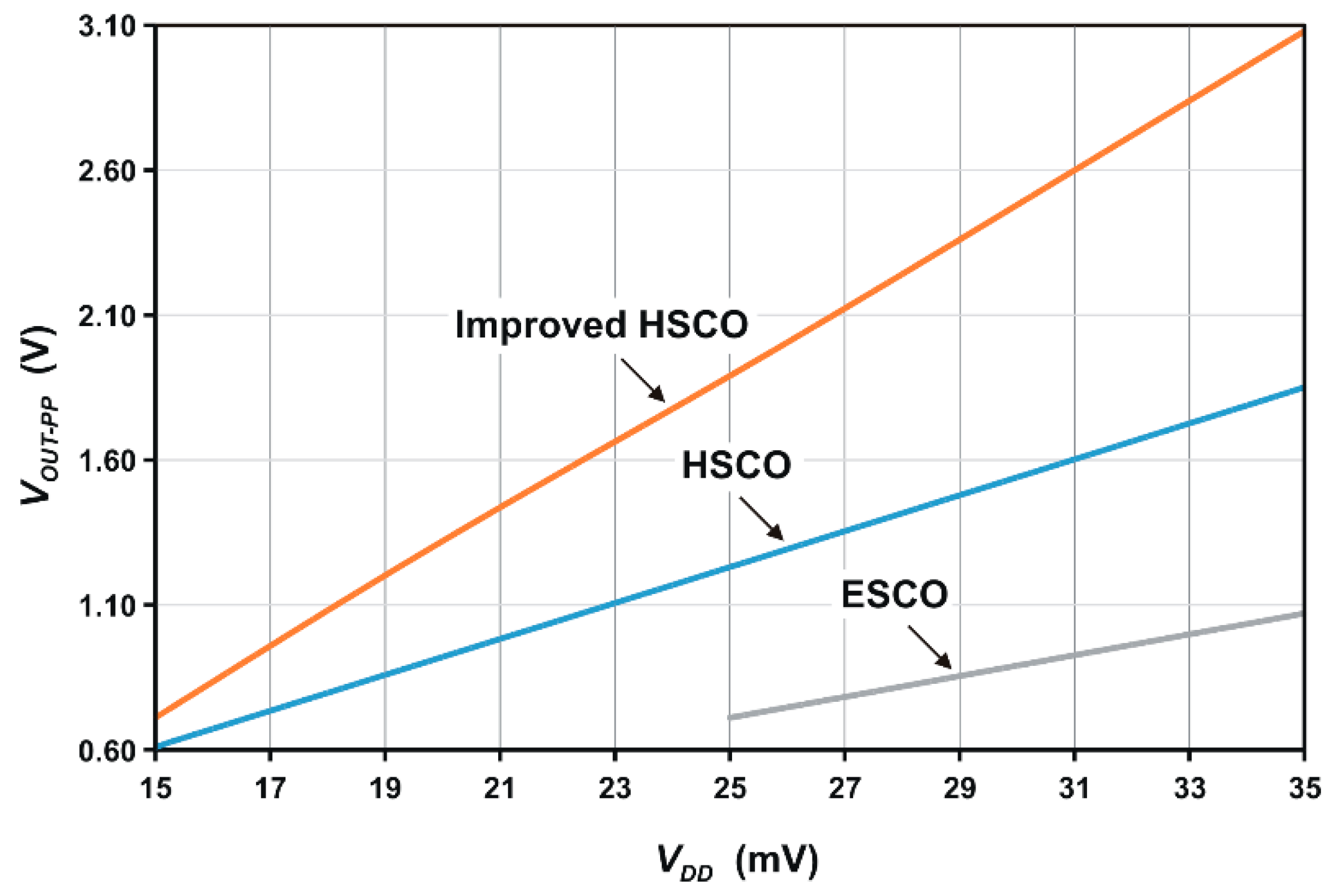
QL = 51 a series of simulations for HSCO and ESCO were performed showing the peak-to-peak value of the output voltage,
vOUT-PP, as a function of the supply voltage
VDD (
Figure 4). For the high inductor quality factor case, a noticeable limitation of the output voltage is observed as the ESCO supply voltage increases. This effect is caused by forward biasing of the pn junction between the transistor drain and substrate.
For all the considered ULV oscillators, the main factor limiting amplitude of the output voltage is a relatively large drain to source conductance of a transistor. Due to this fact, the transistor internal gain is relatively small, especially in HSCO. The gain in this configuration can be increased by increasing the supply voltage
VDD, but this is unfavorable because ULV oscillators should operate for the lowest possible supply voltage. To overcome this limitation, an improved version of HSCO was developed, as shown in
Figure 5.
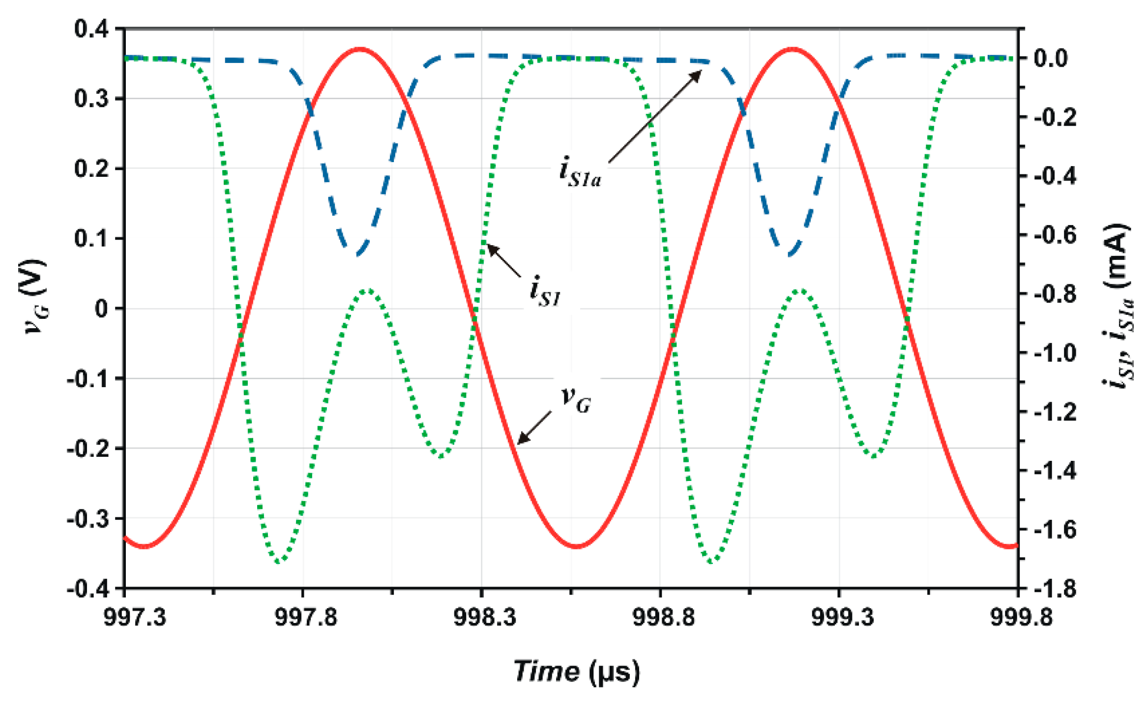
In this oscillator, two transistors connected in parallel are used. M
1 is a transistor with negative or near-zero threshold voltage, whereas M
1a is a low-threshold-voltage transistor. The transistor M
1 plays the same role as in the circuit of
Figure 1c and serves mainly to initiate the oscillation, while M
1a acts as an additional booster which is activated when the output voltage
vOUT reaches a sufficient amplitude. Notice that introduction of M
1a does not lead to noticeable increase of the output conductance of the composite transistor (M
1 + M
1a), because it is switched off for most of the time of the periodic waveform. This transistor is only turned on for short periods of time when the voltage at its gate exceeds a threshold value. Time waveforms illustrating operation of the circuit are shown in
Figure 6.
To demonstrate the advantage of the improved oscillator, the peak-to-peak values of the output voltage as a function of the supply voltage for ESCO, HSCO and improved HSCO are plotted in
Figure 7.
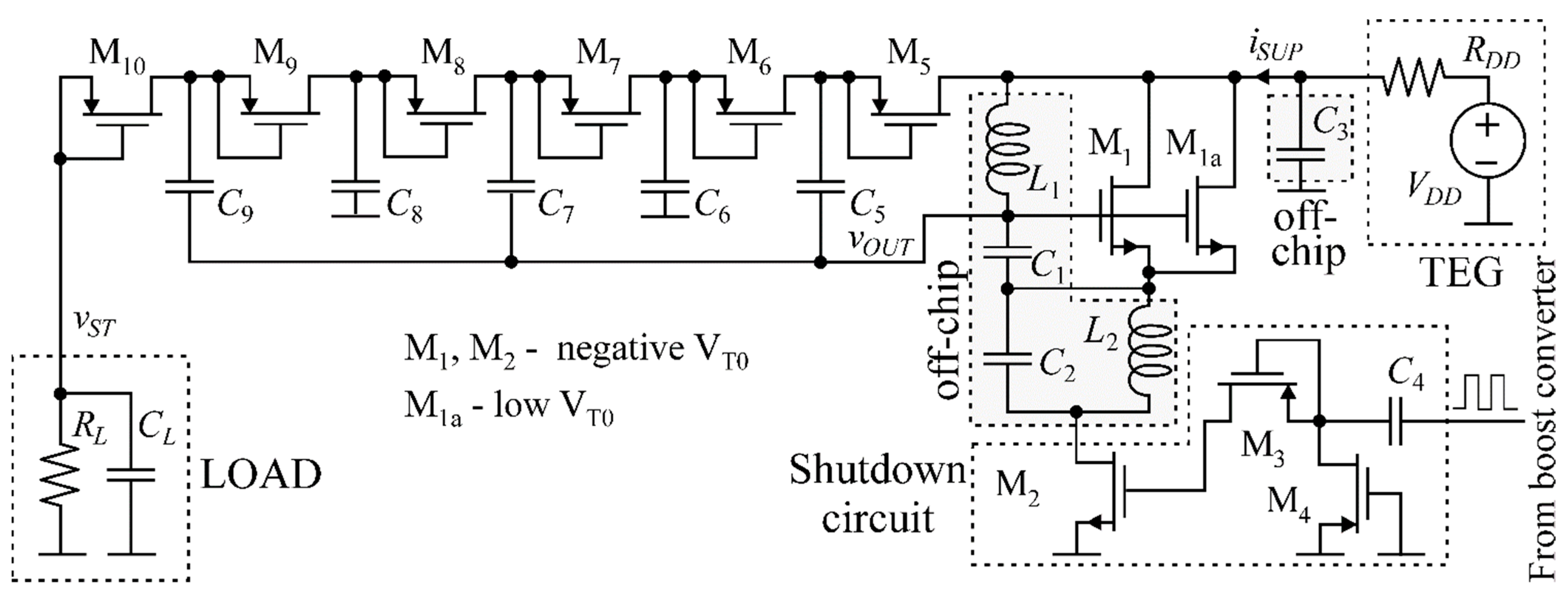
4. Starter Based on the Improved HSCO
The key component of the proposed starter is the improved HSCO oscillator (
Figure 5) which is capable of generating the highest output voltage at low supply voltages (
Figure 7). As the plots in
Figure 3 show, the most advantageous is to use a transistor with a near-zero threshold voltage that operates in the weak inversion region. In the chosen X-FAB 180 nm CMOS technology a zero-threshold-voltage transistor is not available. Thus, the most suitable transistor available was used, namely a n-channel native MOS transistor with a negative threshold voltage of approximately −180 mV. The starter consists of the improved HSCO and a 3-stage voltage multiplier, as shown in
Figure 8.
This solution is additionally equipped with a shutdown circuit which allows its disabling when the main boost converter starts running. The shutdown circuit, consisting of M
2, M
3, M
4, and
C4 is placed in the main current path and allows for complete cutoff of the supplying current. With this solution, when the main boost converter is running, the starter does not increase power consumed from the supply source. M
2 in the shutdown circuit requires a negative voltage to be turned off. This voltage is obtained through rectification (by means of M
3, M
4, and
C4) the square wave voltage applied to control the boost converter switches. The parameters of the starter components are given in
Table 2.
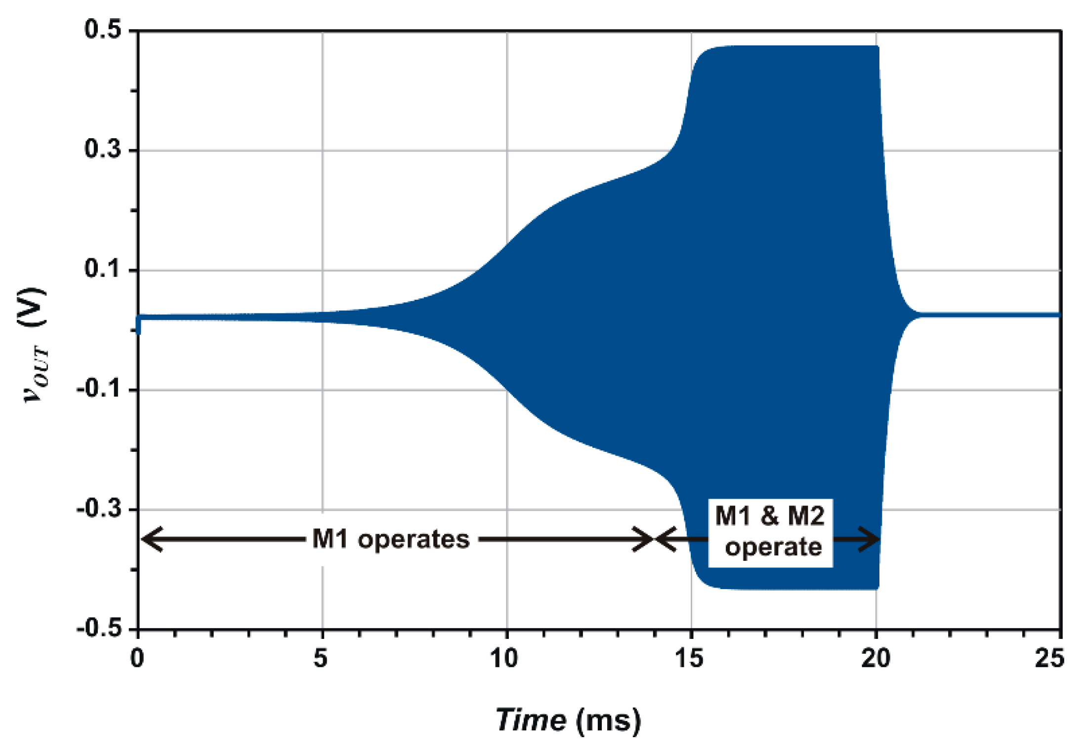
The HSCO startup process is illustrated in
Figure 9 showing the oscillator output voltage,
vOUT, waveform. Two phases of startup can be clearly observed in this plot. The first one, covering the time interval up to about 1.4 ms, is mainly related to operation of the transistor M
1. The second phase begins when the voltage amplitude exceeds the threshold voltage of M
1a. During this time interval, additional current pulses are generated to further increase the amplitude of
vOUT. The plot also illustrates the shutdown moment, which occurs at 2 ms.
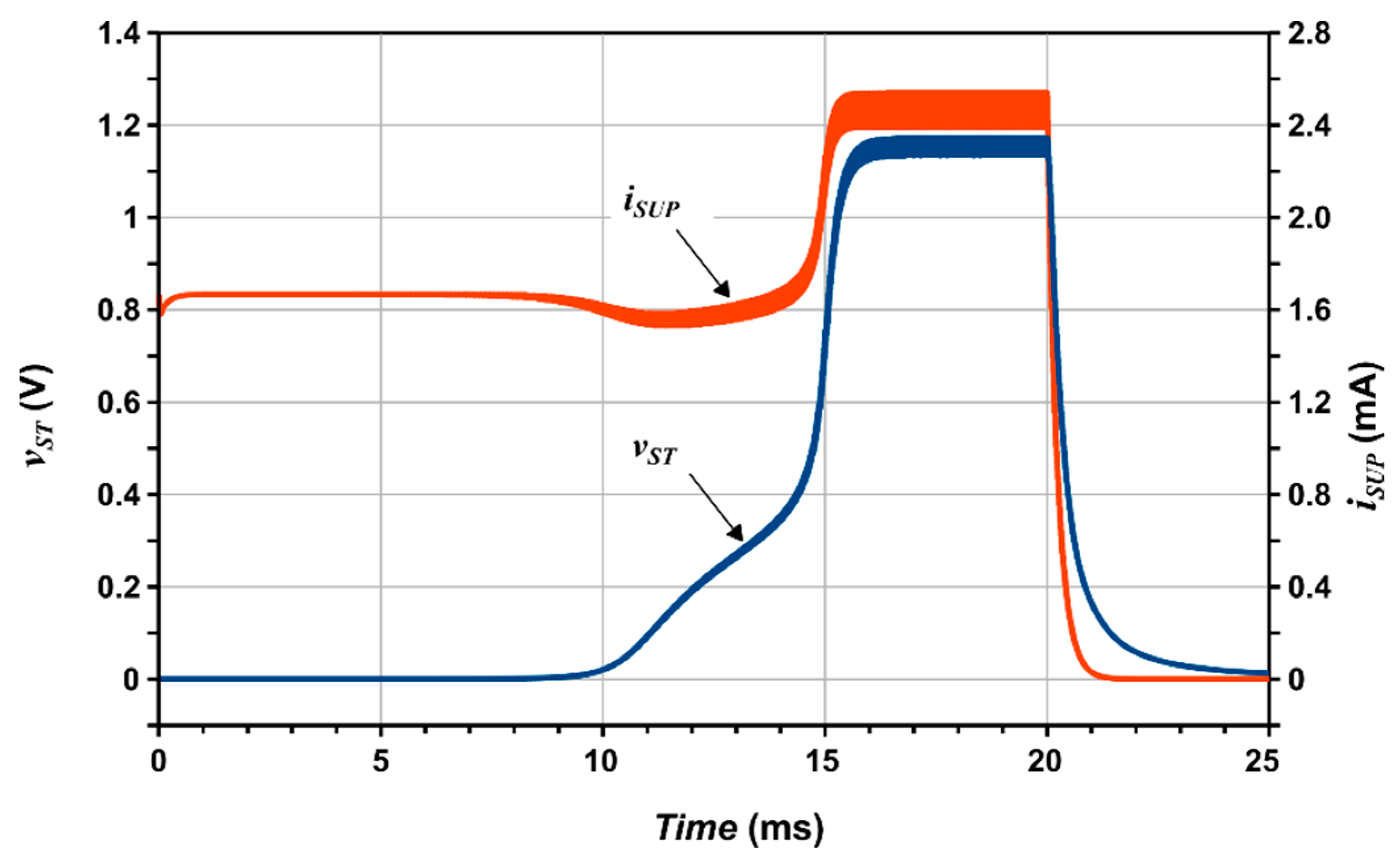
The voltage waveform at the output of the starter,
vST, is shown in
Figure 10. It can be seen that obtaining
vST above 1 V became possible only after boosting the oscillator by the transistor M
1a. The effectiveness of the shutdown circuit can be determined based on the waveform of the current
iSUP sourced from the supply
VDD. In shutdown state,
iSUP decreases to a few tens of nA.
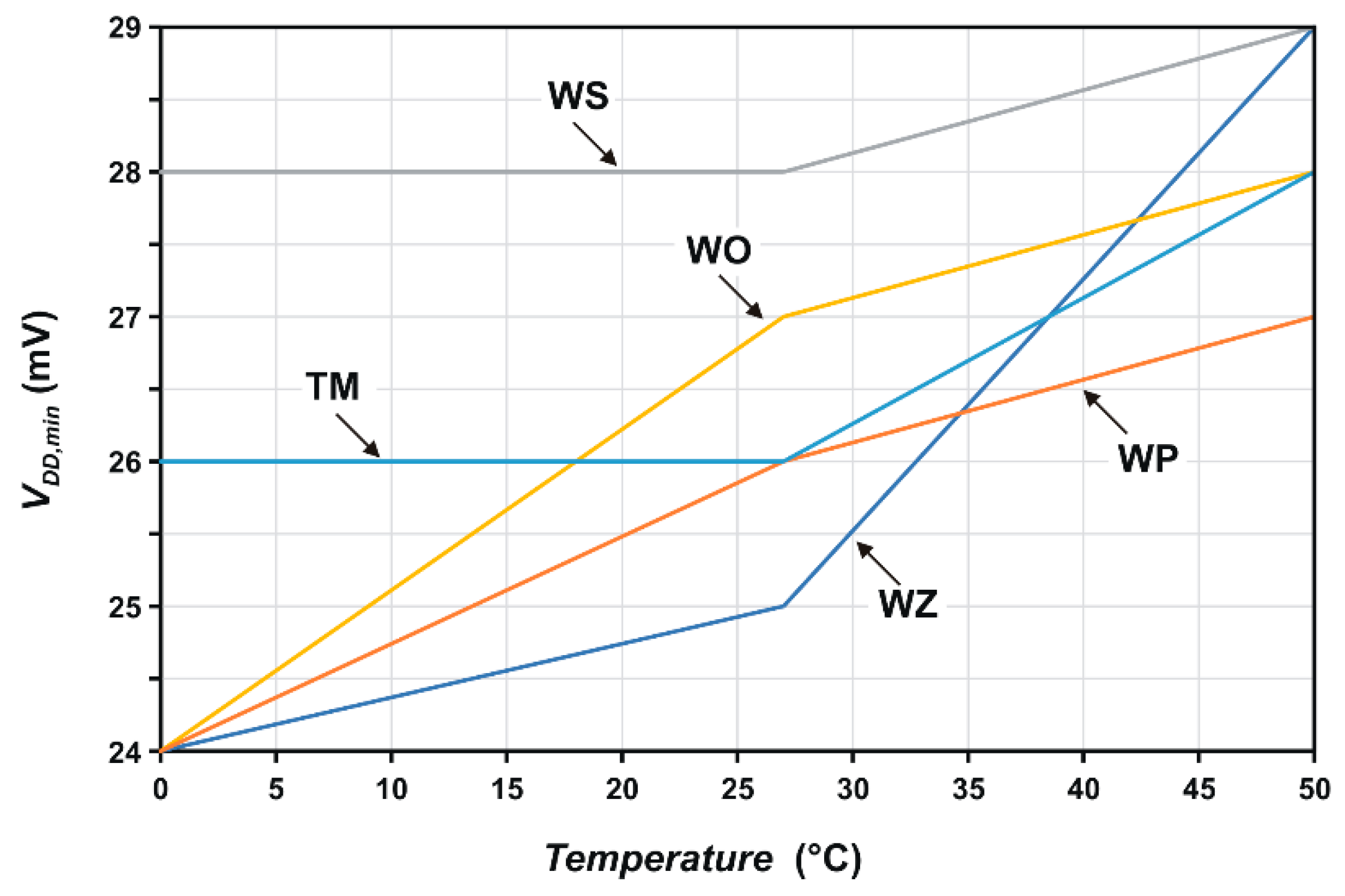
The effect of temperature changes and variations of technology parameters, represented by corners, on the startup voltage is shown in
Figure 11. The worst case startup voltage is 29 mV at 50 °C under worst-speed (WS—slow NMOS, slow PMOS) and worst-zero (WZ—slow PMOS, fast PMOS) corners. Therefore, the proposed starter enables reliable start at supply voltages greater than 29 mV.
A comparison of the main features of the developed starter with solutions reported in the literature is given in
Table 3. The developed starter has a startup voltage which is within the lower range of voltages generated by TEGs. It should be emphasized that the startup voltage can be further reduced for CMOS technologies where zero threshold voltage transistors are available. The developed starter needs two external inductors (
L1,
L2), where
L2 can be of low quality, and two external capacitors (
C1,
C2). In the presented solution, the oscillation frequency is about 1 MHz, but can be increased to more than 10 MHz, allowing further reduction of external inductors and capacitors leading to a higher degree of miniaturization. The power efficiency of the proposed starter is approximately 1.5%. However, it should be emphasized that such low efficiency is not important since the starter operates only in the initial phase of the converter start-up and then is immediately turned off.


