1. Introduction
A matrix converter is a compact ac-ac power converter, in which dc-link capacitors are not used [
1]. A matrix converter is commonly divided into a one-stage matrix converter (OSMC) and two-stage matrix converter (TSMC) with the same transfer function, and the TSMC is divided into the rectifier stage and the inverter stage, where the rectifier stage is based on a conventional three-phase full-bridge [
2,
3]. In recent years, this converter family has been globally studied in power topologies, control schemes, and trends [
4,
5,
6,
7]. Because of the absence of dc-link capacitors, the input side of the matrix converter directly connects the output side, coupling the input and output currents and voltages [
4,
5]. Compared with the traditional control schemes of the matrix converter, like the Venturini method [
4,
6], direct power control [
7], and so on, the space vector modulation (SVM) method has been proved as a suitable control strategy [
8,
9]. In SVM, the input and output voltages and currents are considered using space vectors [
10,
11]. However, model predictive control defies SVM with the emergence of developing digital processors and power devices [
12,
13,
14]. In this control scheme, the matrix converter’s future behaviors are predicted and optimized by minimizing a user-defined and model-based cost function, featuring many advantages such as simpler modifications, easier implementations in modern digital control platforms, and so on [
15,
16,
17].
However, model predictive control (MPC) defies SVM with the emergence of developing digital processors and power devices [
12,
13,
14]. In this control scheme, the matrix converter’s future behaviors are predicted and optimized by minimizing a user-defined and model-based cost function, featuring many advantages such as simpler modifications, easier implementations in modern digital control platforms, and so on [
15,
16,
17]. In [
15], a simple digital predictive current control strategy without the modulation stage was proposed for the two-level four-leg inverters, where both balanced and unbalanced loading conditions were considered. In [
16], a new speed finite control set model predictive control (FCS-MPC) algorithm was proposed and applied for a permanent-magnet synchronous motor driven by a matrix converter, in which the comparison between classical modulation methods and the FCS-MPC was carried out with the simulation and the experiment. In [
17], a simplified FCS-MPC method was proposed to reduce the calculation efforts for the application in matrix converter-fed permanent magnet synchronous motors, including a new cost function controlling currents during both speed transient and steady-state conditions and an input filter observer increasing the system reliability. However, the major weakness of the FCS-MPC is the lack of modulation, where only one optimal switching state is determined and applied in one sampling period. Owing to this weakness, variable switching frequency and a broad harmonic spectrum are produced, which lead to unexpected ripples in the system and affect the system’s power-quality performance [
18]. To overcome these problems, the modulated model predictive control (MMPC) strategy is introduced [
19,
20,
21,
22,
23], where the switching frequency is kept constant and more than one switching states are determined and applied by the two independent cost functions of the rectifier and the inverter in an appropriately fixed switching instant. In [
19], the MMPC strategy was proposed for shunt active filters, where a cost function ratio for output vectors-based modulation algorithm was included in the MPC. In [
20], a three-vector-based low-complexity model predictive direct power control scheme was proposed and applied for doubly fed induction generators, aiming to eliminate the steady-state errors and reduce the current ripples. In [
21], the MMPC was proposed and applied for the modular multilevel converters in voltage source converter-high voltage dc systems, where modulated switching signals with a fixed switching frequency were applied to minimize the ac line current ripples. In [
22], a continuous control set model predictive control (CCS-MPC) scheme was proposed for the constant voltage constant frequency inverters, in which a fuzzy logic approach corrected the input voltage commands to obtain a faster transient response and smaller steady-state error. In [
23], a comparative study of the FCS-MPC and the CCS-MPC for induction machine in terms of their design and performance was conducted, in which the behaviors were assessed by applying reference and disturbance steps to the system in different operational modes. The CCS-MPC was proved to feature smaller current ripples and could cope with a less powerful DSP than the FCS-MPC.
Besides, some research work has been done about the optimal pulse patterns [
24,
25]. In [
24], an optimal six vector switching pattern based on the SVM has been proposed for matrix converters to reduce harmonics and switching losses, in which a faster response, lower harmonics, and lower losses have been obtained than those using the five vector pattern. The weaknesses of this method are larger 1/2 and 3/2 sampling frequency harmonics and increased complexity. In [
25], an offline computed optimal pulse pattern has been proposed based on modulated model predictive control for a delta-connected modular multilevel converter, which facilitates the shaping of the grid current spectrum at low switching frequencies.
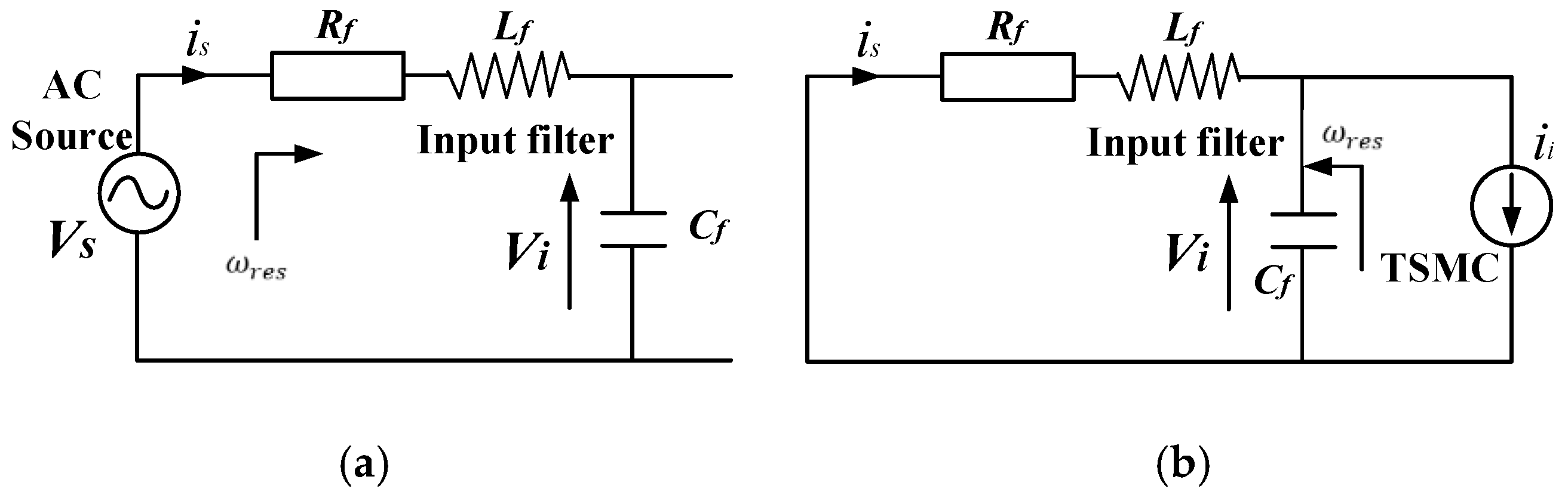
For matrix converters, an input filter is usually employed to prevent the line-current ripples. However, the converter itself and the potential harmonics in the ac source usually excite the series resonance and the parallel resonance of the input filter, leading to highly distorted line-side currents, which can also transfer to the load side because of the direct topology [
26,
27,
28,
29,
30]. To solve this problem, several damping methods have been proposed. In [
26], the researcher proposed a passive damping method by placing a damping resistor in parallel with the filter inductor, which can mitigate the resonance but draw more power losses and less attenuation around switching frequency. Besides, as discussed in [
27], this method is not suitable for some specific applications, such as a generator source where stator inductance acts as the filter inductor. To improve this, some active damping methods have been proposed, where physical resistors are not used [
28,
29,
30]. In [
28], the filtered capacitor voltages were added into the input current references in the active damping method, which can suppress the oscillations effectively but only work for the independent control of input currents. In [
29], an iterative design method in consideration of the most significant grid-current harmonics is proposed to decide the filter parameters, using a PWM strategy. In [
30], another active damping method is proposed by modifying the input current reference, using the SVM strategy. This method is not applicable to the predictive control where the input current reference is not required. Most of these schemes include complex control methods.
To solve these problems above, this paper proposes a novel predictive control method with optimal switching sequence (OSS) and input filter resonance suppression (IFRS) for the TSMC. The main contributions of this paper are as follows:
A vector modulation-based model predictive control (VMMPC) strategy is proposed, which features the controllable source reactive power and the controllable output currents with fixed switching frequency output waveforms.
In this paper, the advantage of the VMMPC strategy compared with the conventional MPC (CMPC) is firstly proved using the principle of vector synthesis and the law of sines in the vector distribution area.
An optimal switching sequence is proposed, which can ensure safe zero-current switching operations and reduce the switching losses. This pattern can simplify the commutation of the TSMC and avoid complex commutation strategies (e.g., four-step commutation) in traditional control methods;
A novel input filter resonance suppression method is proposed and implemented in the VMMPC for the TSMC, which shows good damping performance and easy implementation.
The paper is organized as follows: In
Section 1, an introduction to the research problem is carried out.
Section 2 describes the TSMC mathematical system model.
Section 3 presents the proposed VMMPC with the OSS and the IFRS and validates the advantage of the VMMPC over the CMPC in theory.
Section 4 shows the simulation results and discussion.
Section 5 demonstrates the experimental results and discussion.
Section 6 is the conclusion.
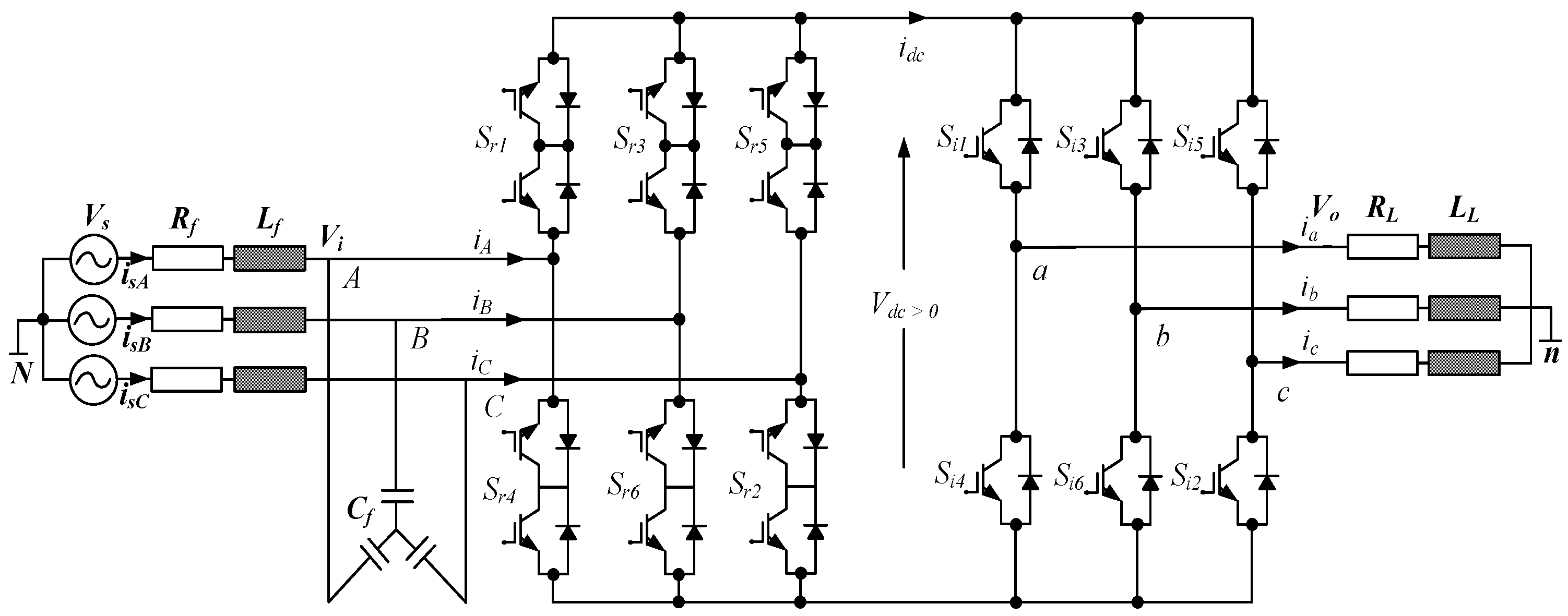
2. TSMC System Model
The TSMC system is composed of the rectifier stage and the inverter stage, whose topology is shown in
Figure 1 [
13]. This configuration can simplify the commutation strategy.
For the rectifier stage,
can be calculated with
and
as:
where
are the switching functions,
is the DC-link voltage and
is the input voltage. Besides,
are calculated with
and
as:
For the inverter stage, the DC-link current
is calculated with the inverter switching functions
and the output current
:
where
are the switching functions for the inverter stage. Moreover, the output voltage
is calculated with
and
In the TSMC system, only six switching states for the rectifier stage and eight switching states for the inverter stage are valid as shown in
Table 1 and
Table 2.
As seen in
Figure 1,
Table 1 and
Table 2,
are the three-phase input currents,
,
are the three-phase input line voltages,
,
,
are the three-phase output line voltages, and
,
,
are the three-phase output currents.
In addition, in order to avoid over-voltages and harmonics distortions, an input filter is implemented with its model described as follows [
7]:
where
and
represent the input filter inductance and capacitance, and
is the resistance of
.
Moreover, the load model can be described as follows [
7]:
where
and
are the load resistance and inductance.
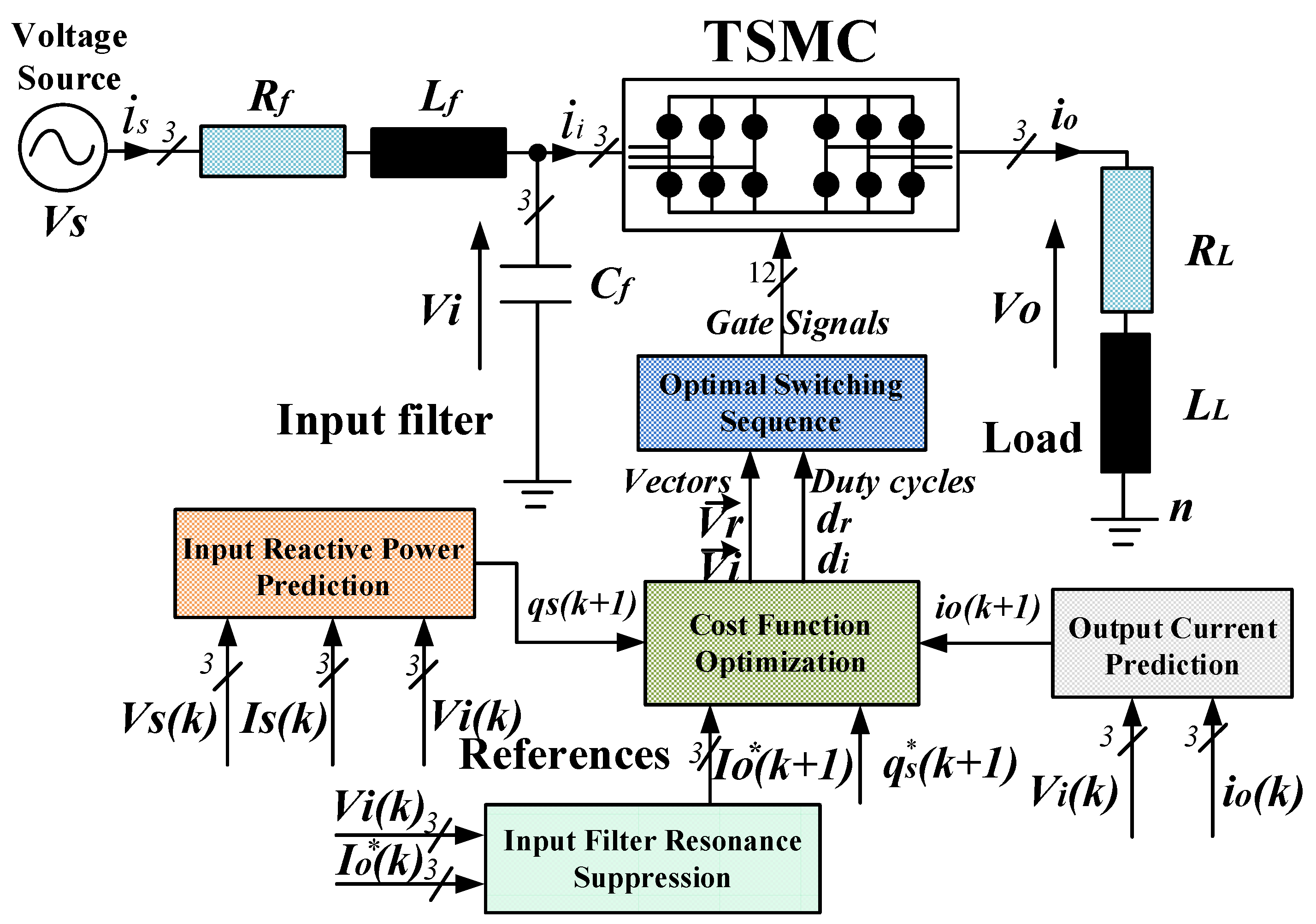
3. Vector Modulation-Based Model Predictive Control Strategy with Optimal Switching Sequence and Input Filter Resonance Suppression
The proposed control strategy for the TSMC system is shown in
Figure 2, which consists of source reactive power prediction, output current prediction, cost function optimization, the OSS, and the IFRS.
Firstly, the IFRS generates the updated output-current reference , then and are calculated with the output current prediction and the source reactive power prediction, which are the predicted values at the (k + 1)th sampling instant.
Thus, with the references and , the optimal switching states are selected by the cost functions, which approach and at the end of the (k + 1)th sampling instant.
Finally, the OSS scheme is employed to ensure zero-current switching operations, where the vectors are symmetrically arranged.
3.1. Source Reactive Power Prediction and Output Current Prediction
For the input side, the discrete state-space model can be obtained as follows:
where
represents the sampling time,
,
,
and
represent the input filter resistance, inductance, and capacitance. Thus, the predicted source reactive power
can be calculated as:
where
represent the source voltage and
are the predicted source current in
reference frame.
In the same way, the discrete state-space model of the output stage is obtained as follows:
where
,
),
and
are the load resistance and inductance.
3.2. Cost Function Optimization
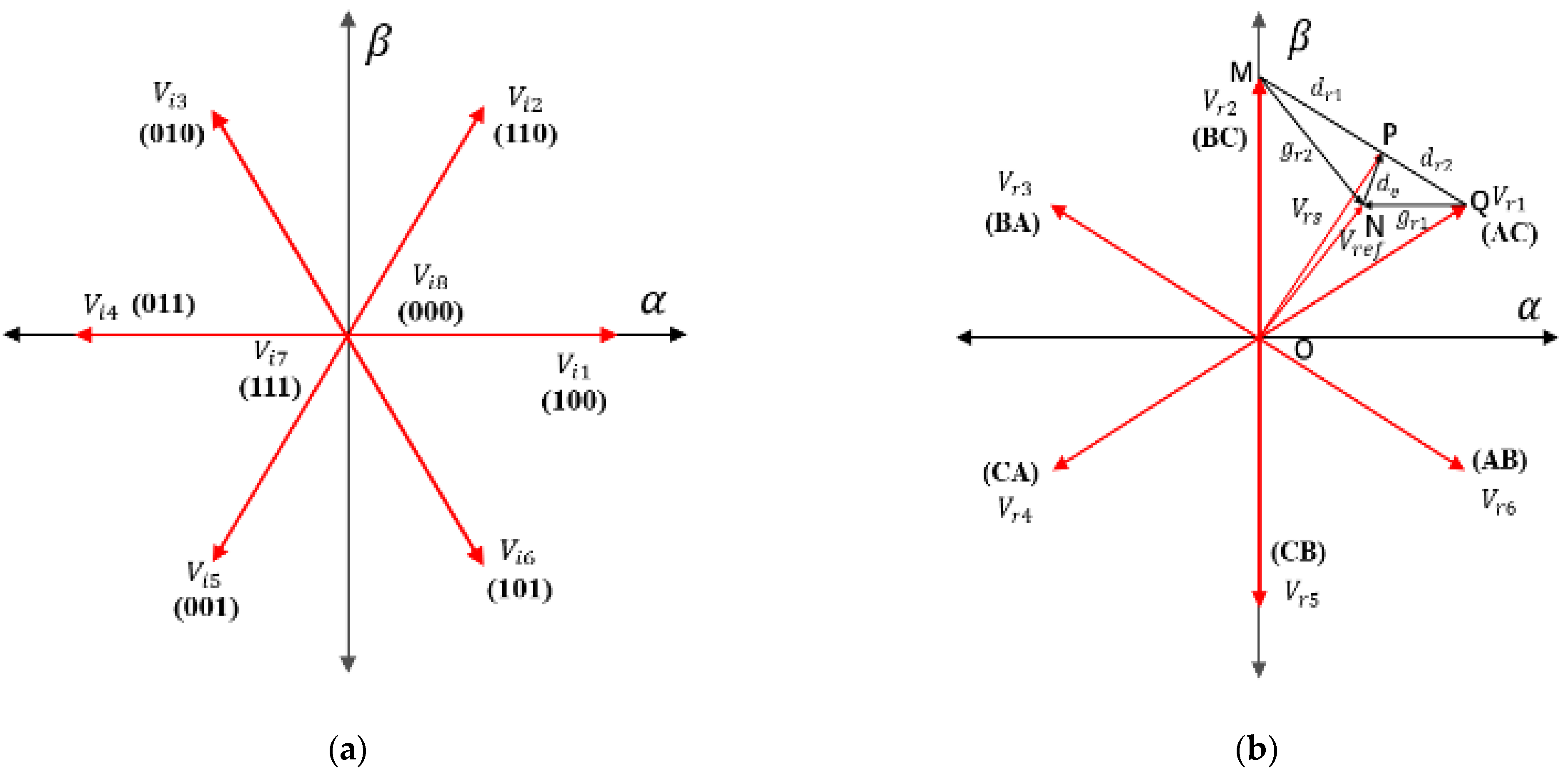
For the inverter stage, eight voltage space vectors are valid (six active vectors and two zero vectors) as shown in
Figure 3a, and associated with switching states in
Table 2. The proposed VMMPC strategy employs two valid adjacent vectors
and one zero vector
or two zero vectors (if necessary).
It should be noticed that the sampling frequency is much higher than the fundamental frequency, and thus, the control objective error
can be approximated by using a time-weighted value
[
22,
23].
where
represents the error when only one vector
is applied for the whole sampling period
and
is the duty cycle of
.
Define
as the root mean square (RMS) value of all the weighted errors, which can be calculated as
In Equation (13),
represents the mean value of the weighted errors and
is the variance of the weighted error as
Considering that
, minimizing
yields minimum values of
and
. Thus, the duty cycles used by the proposed VMMPC strategy can be obtained based on minimizing (13). That is
Here, this optimization problem could be solved by the Lagrange multipliers method. In order to find the stationary points of a function
subject to the constraint
, define the Lagrangian function as
Therefore, the optimization problem yields minimization of the following function:
where
are the cost function values for three active vectors
and
are the duty cycles respectively. In the Lagrange multipliers method, the constraint is
Substituting (18) and (20) into (17), the Lagrangian function yields
The gradient of
can be calculated as
Substituting (21) into (22) yields
Considering the minimization condition
Using (23) and (24), the duty cycles can be calculated as
Thus, the synthesized vector
and the total cost function
can be obtained as follows:
Similarly, for the rectifier stage, there are six active current space vectors, as shown in
Figure 3b, associated with switching states in
Table 1. The proposed VMMPC scheme employs two valid adjacent vectors
and assesses two respective cost functions
. The duty cycles
can be obtained as:
With
, the total cost function
and the synthesized vector
can be evaluated at every sampling period as:
3.3. Comparision between the Proposed VMMPC and the CMPC
From
Figure 3b, it is obvious that the length of the segment NQ is
, which is defined as the error when only the vector
is applied, and the length of the segment MN is
, which is defined as the error when only the vector
is applied respectively.
From Equations (29) and (32)–(34), it can be obtained that:
From Equations (33) and (34), obviously that the end-point of the synthesized vector (tagged as P) should be located on the segment MQ, and the length of the segment MQ is . Besides, the length of the segment MP is , and the length of the segment MP is , respectively.
Considering Equations (29), (33), and (34) and the law of sines, (35) can be obtained:
Moreover, since
, thus
, (36) can be obtained as:
In this scenario, two conditions are always fulfilled:
It can be inferred that . Considering the law of sine, is obtained. Similarly, is deduced. Both these two conditions can prove the advantages of the VMMPC strategy when compared with CMPC in which only one switching state is selected and applied for the whole sampling instant.
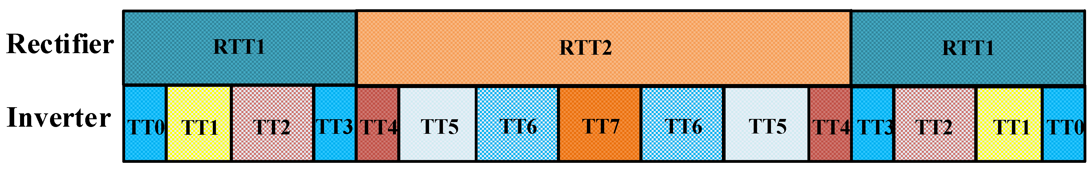
3.4. Zero-Current Switching Sequence
Since no dc-link capacitors are used in the TSMC topology, the rectifier stage connects the inverter stage directly. In this paper, a zero-current switching sequence is proposed, in which the switching sequences of the rectifier and the inverter are strictly coupled. The OSS proposed is shown in
Figure 4.
The duty cycles
for the inverter are calculated as:
Moreover, the duty cycles
for the rectifier stage are
From Equations (38) and (39), it is obvious that the rectifier state commutation always occurs, when zero voltage vector is implemented for the inverter and . In such a way, zero-current switching operations and reduction of the switching losses of the TSMC are achieved, simplifying the commutation strategy of the TSMC.
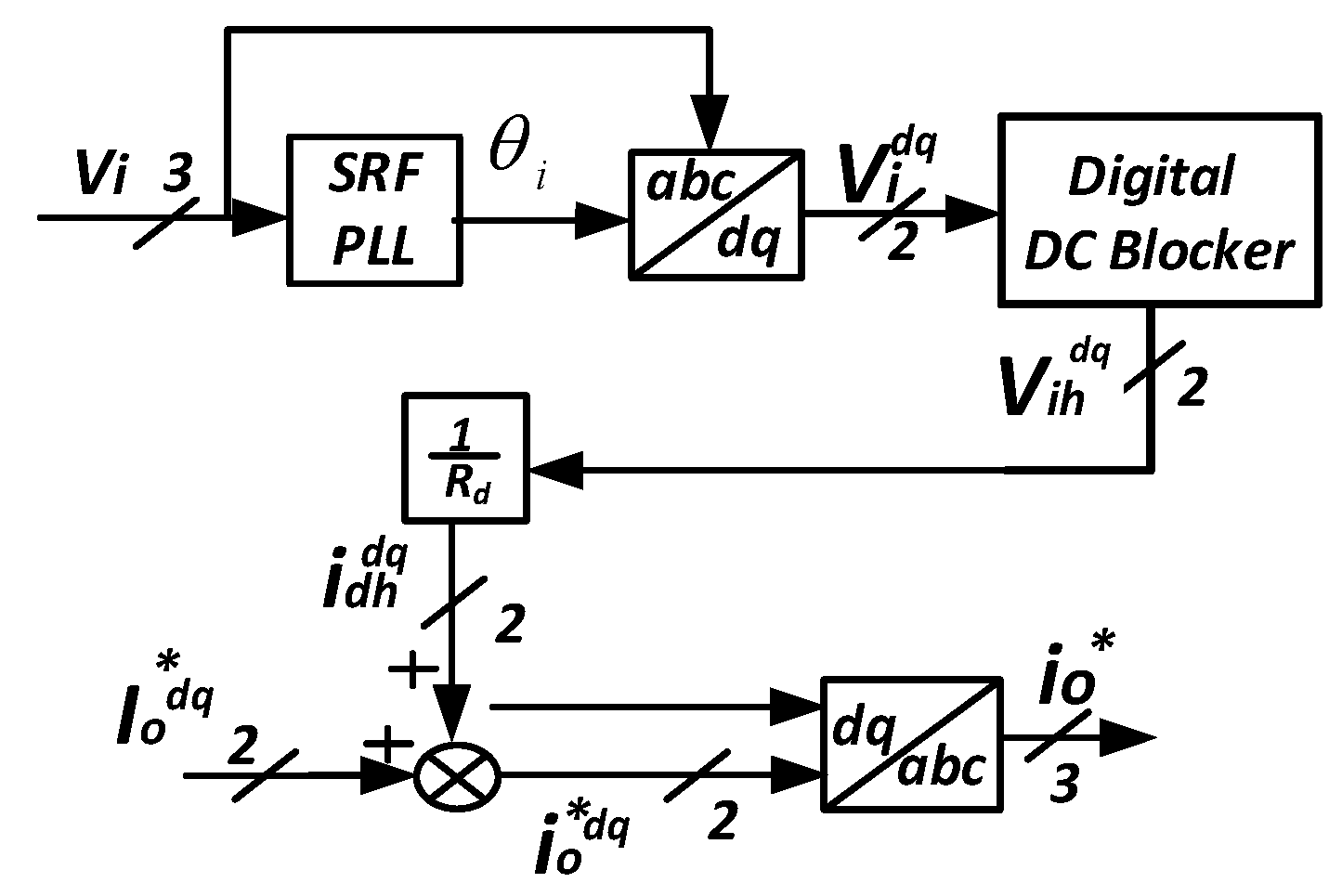
3.5. Input Filter Resonance Suppression
As mentioned before, the input filter resonance is easier to be inspired by the model predictive control. The OSS is proposed as shown in
Figure 5.
Initially, the scheme considers
in a dq reference frame based on the abc/dq transformation, which is realized by the synchronous-reference frame phase-locked loop (SRF-PLL). Then, the harmonic components
in the dq reference frame can be obtained by passing through a digital DC-blocker filter, which blocks the fundamental component of the voltage. Finally, the damping harmonic currents
can be calculated as:
where
denotes all the input voltage harmonic components in
, and
denotes the damping harmonic currents,
is a virtual resistive damper placed in parallel with the input filter capacitor
. Then, the modified output-current reference is obtained as follows:
where
is the unchanged reference of output current in dq reference frame, and
is the updated output current reference in dq reference frame.
The transfer function of the input filter is
Considering the damping current
It is clear that the damping current delay results from the dynamics of the digital dc blocker and the (
k + 1)
th variables. Then, this paper uses the following approximation:
Besides, a low-pass filter is defined as:
By using a bilinear transformation, (45) can be rewritten as:
Thus, the harmonic current can be obtained as
and
Hence, the idealized open-loop active damping system is approximated by using the damping current gain 1/Rd and the parallel filter impedance as
where
is the sampling time,
and
are the input filter inductance and capacitance,
is the resistance of
. The parameter “a” in Equations (46) and (49) is set to 0.99999, which is the parameter of the digital DC blocker,
is the active damping resistor. From (49), based on the phase and gain margins of the open-loop gain, the minimum damping resistance for the approximated system stability can be determined. The idealized system becomes unstable when an active damping resistance is under 25Ω. In practical applications, a much larger resistance than the minimum necessary for the approximated system stability is used. Considering reasonable phase and gain margins, and the suppression of the load current distortions, the recommended resistance value of the active damping resistor is between 25 and 83 Ω.
4. Simulation Results
In order to validate the performance of the proposed method, simulation results in Matlab/Simulink have been carried out and the parameters of the simulation model are shown in
Table 3.
The input filter resonance can be excited by the utility (series resonance) due to the potential fifth and seventh harmonics in the ac source (seen in
Figure 6a), and also by the converter itself (parallel resonance seen in
Figure 6b). The highly distorted line-side currents are also reflected in the load side because of the direct topology of the TSMC (seen in
Figure 1). Normally, the filter resonant frequency should satisfy both one decade above the input supply frequency
and one decade below the switching frequency
to minimize the effect of the resonance introduced by the filter [
31]. That is
In this paper, the resonant frequency is designed and situated nearly at the seventh harmonic of the source system to excite the resonant situation, in which the TSMC system performance can be compared with the IFRS and without the IFRS.
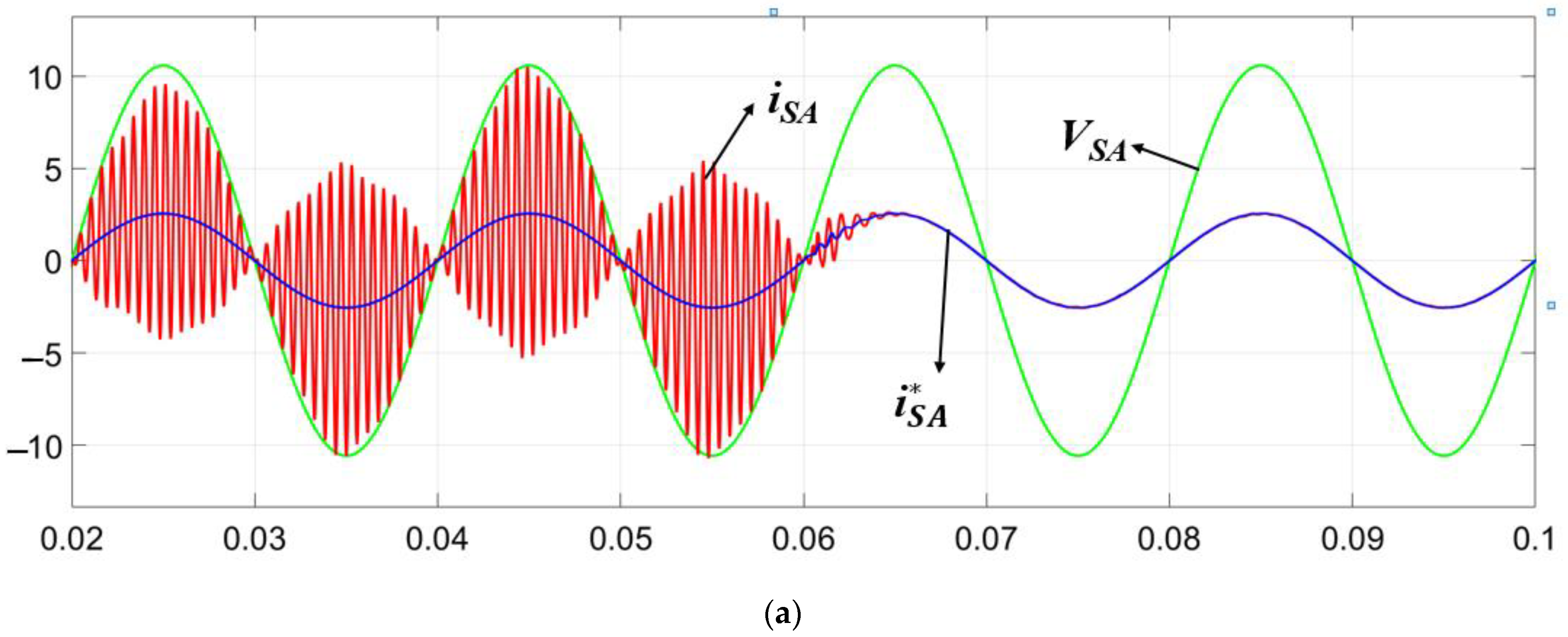
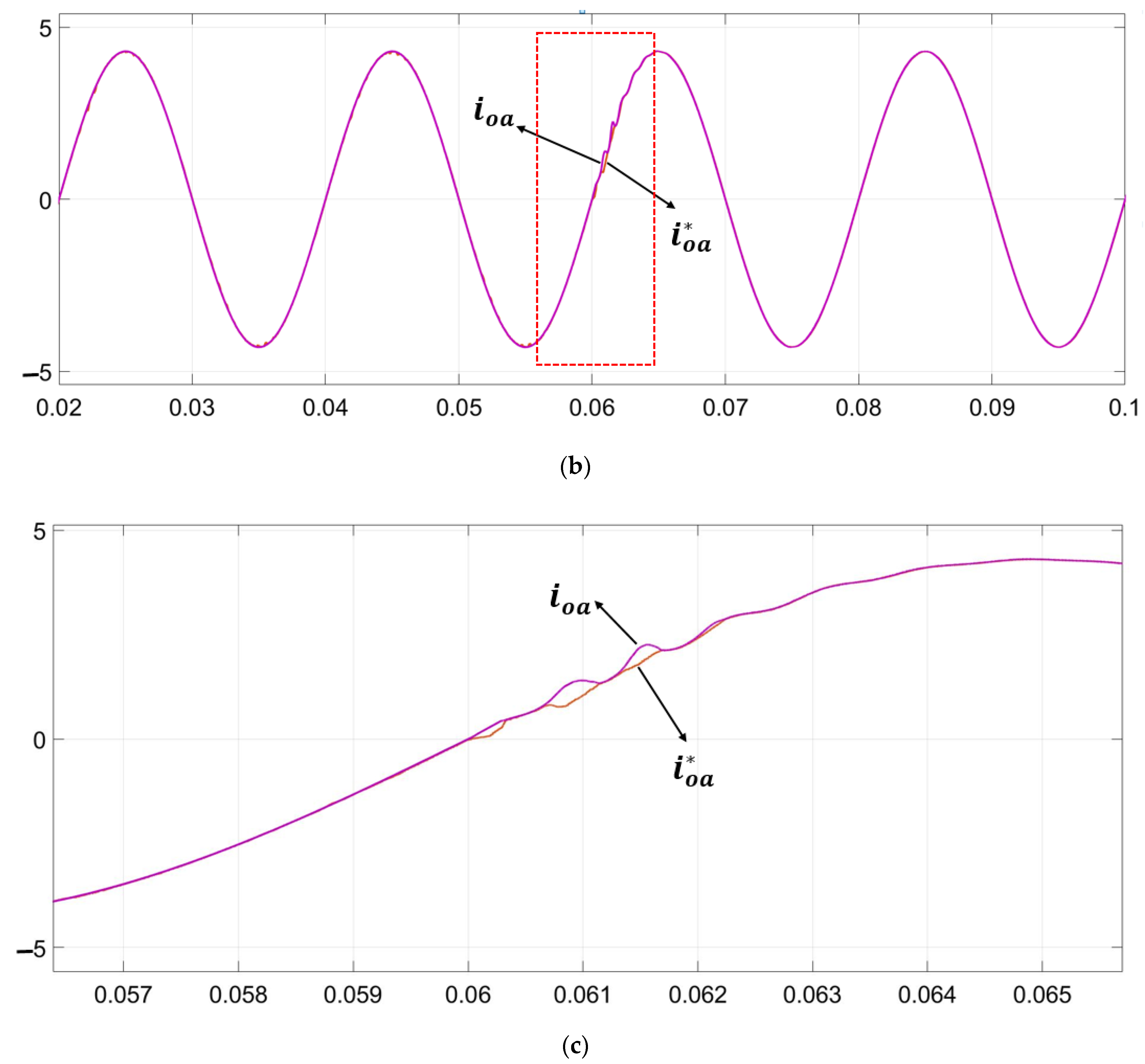
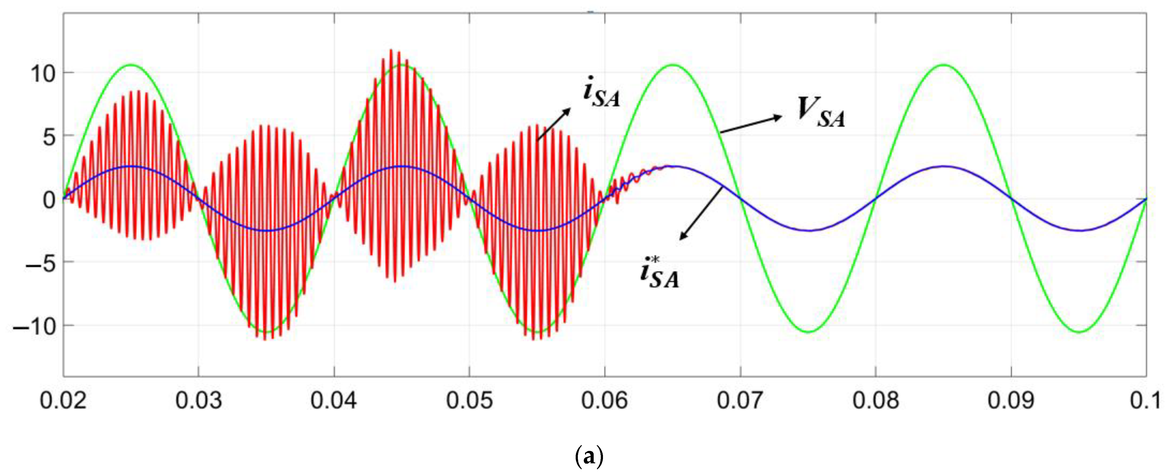
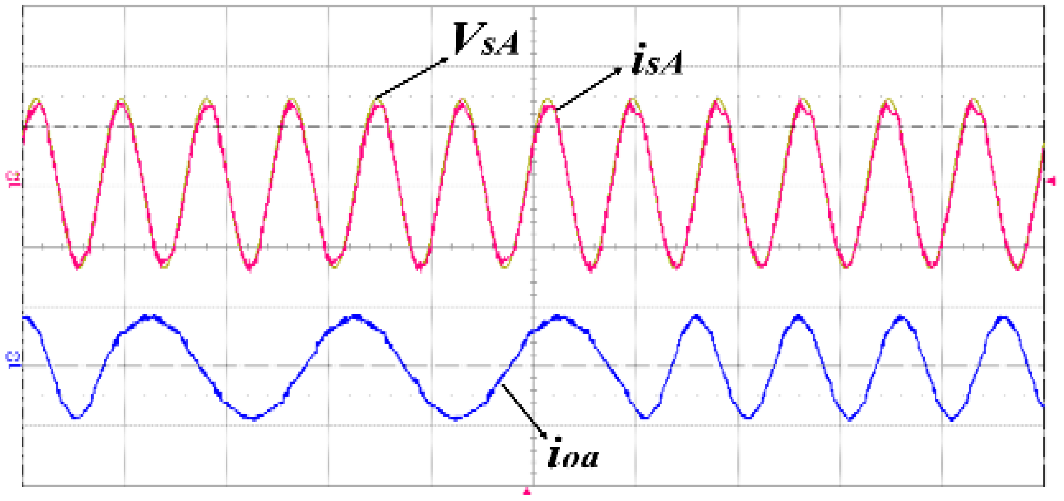
The source voltage and current, and the source-current reference of the input phase A are demonstrated in
Figure 7a, and the output current and its reference of the output phase a are shown in
Figure 7b. As can be seen from
Figure 7, the IFRS is added at t = 0.06 s. Before that, the source current is highly distorted because of the resonance of the input filter. In contrast, the source current is greatly improved with an almost sinusoidal waveform after t = 0.06 s, achieving a very good tracking to its reference. At the same time, an almost sinusoidal waveform of the output current is obtained in
Figure 7b, approaching its reference.
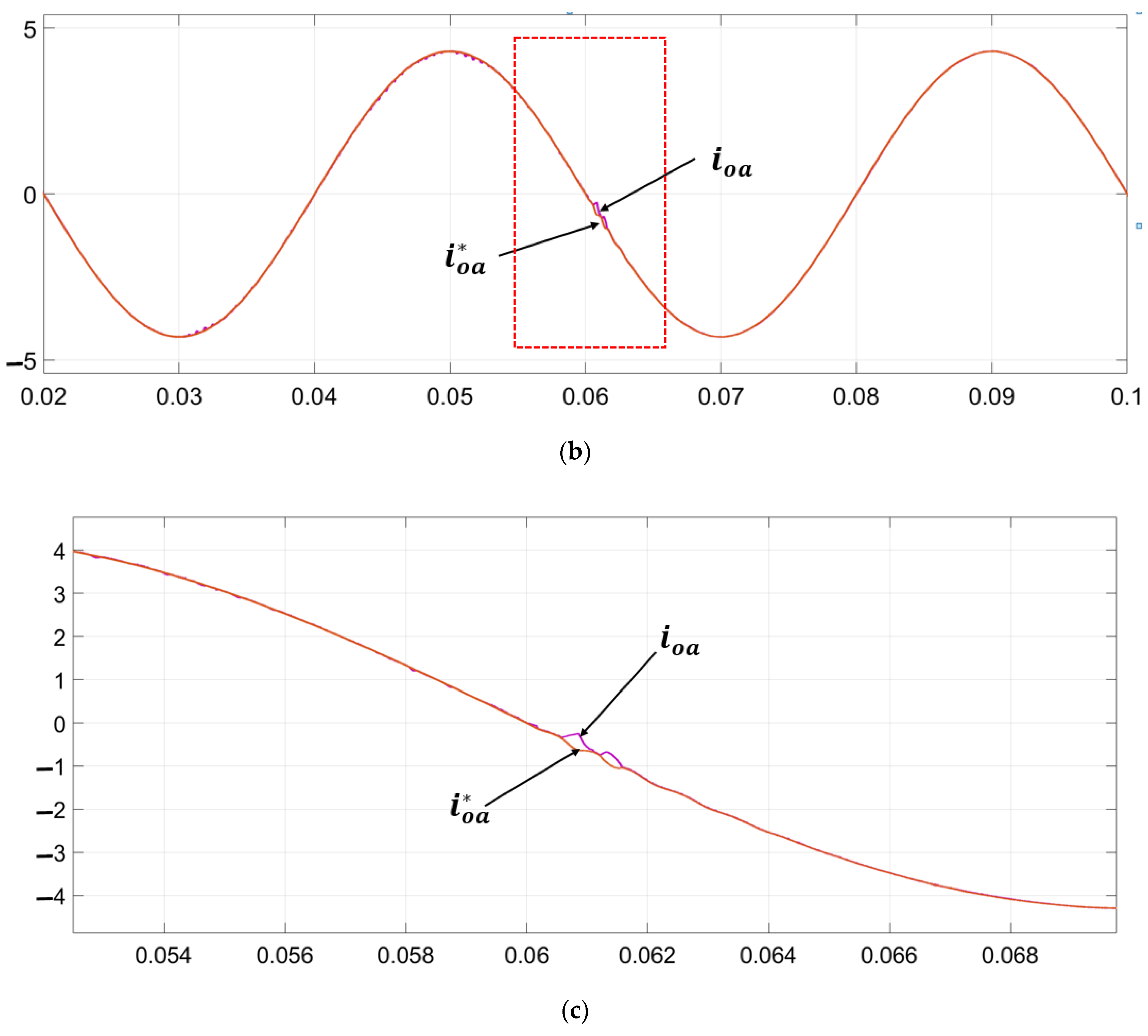
Figure 8 shows the results of another simulation group, where the output-current frequency reference is set to 25 Hz and the other control parameters remain the same. As shown in
Figure 7 and
Figure 8, the IFRS can greatly improve the quality of source current in spite of frequency variations. Besides, the source current is in phase with the source voltage, indicating that the source reactive power is minimized based on Equations (10) and (30).
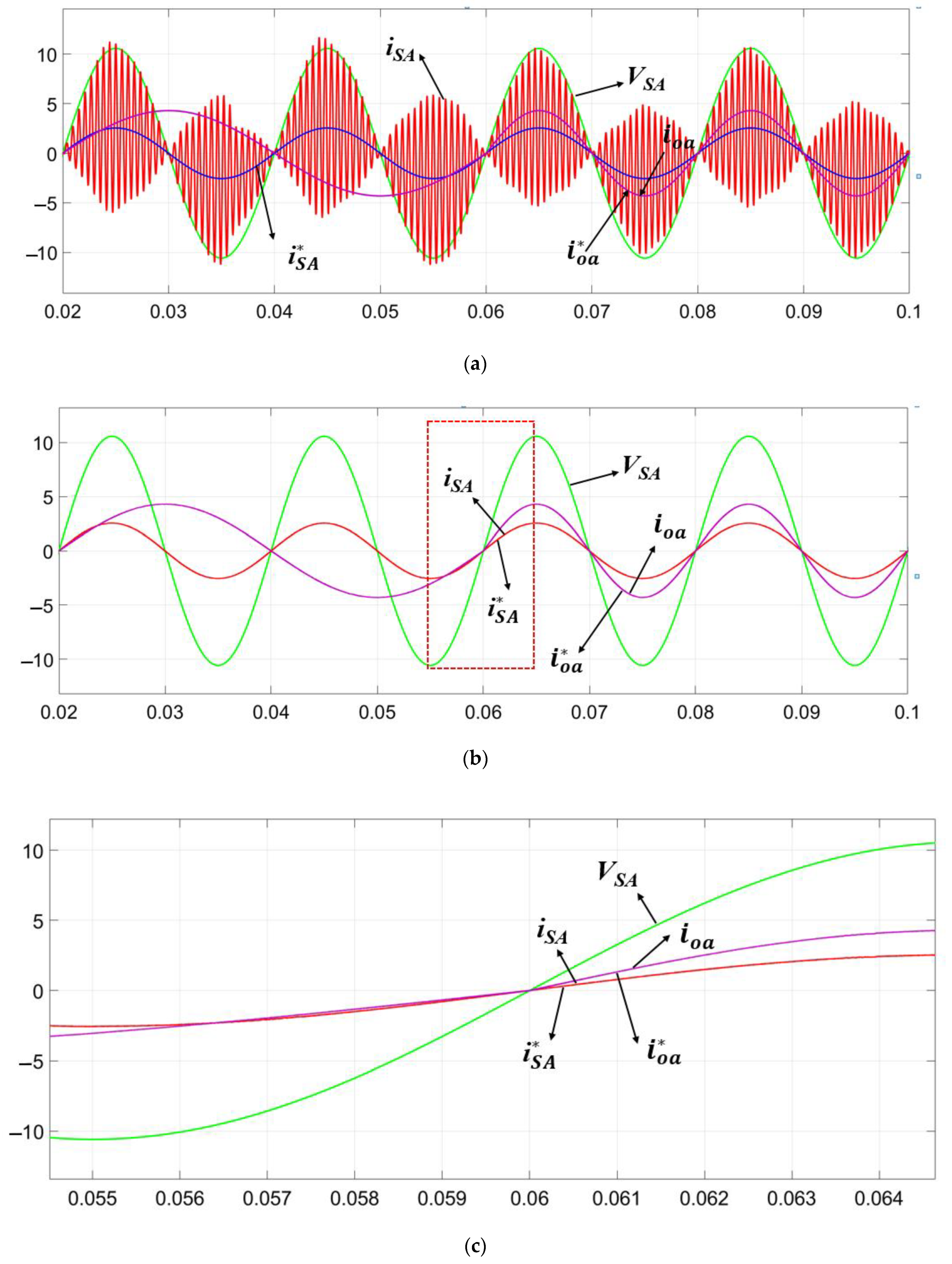
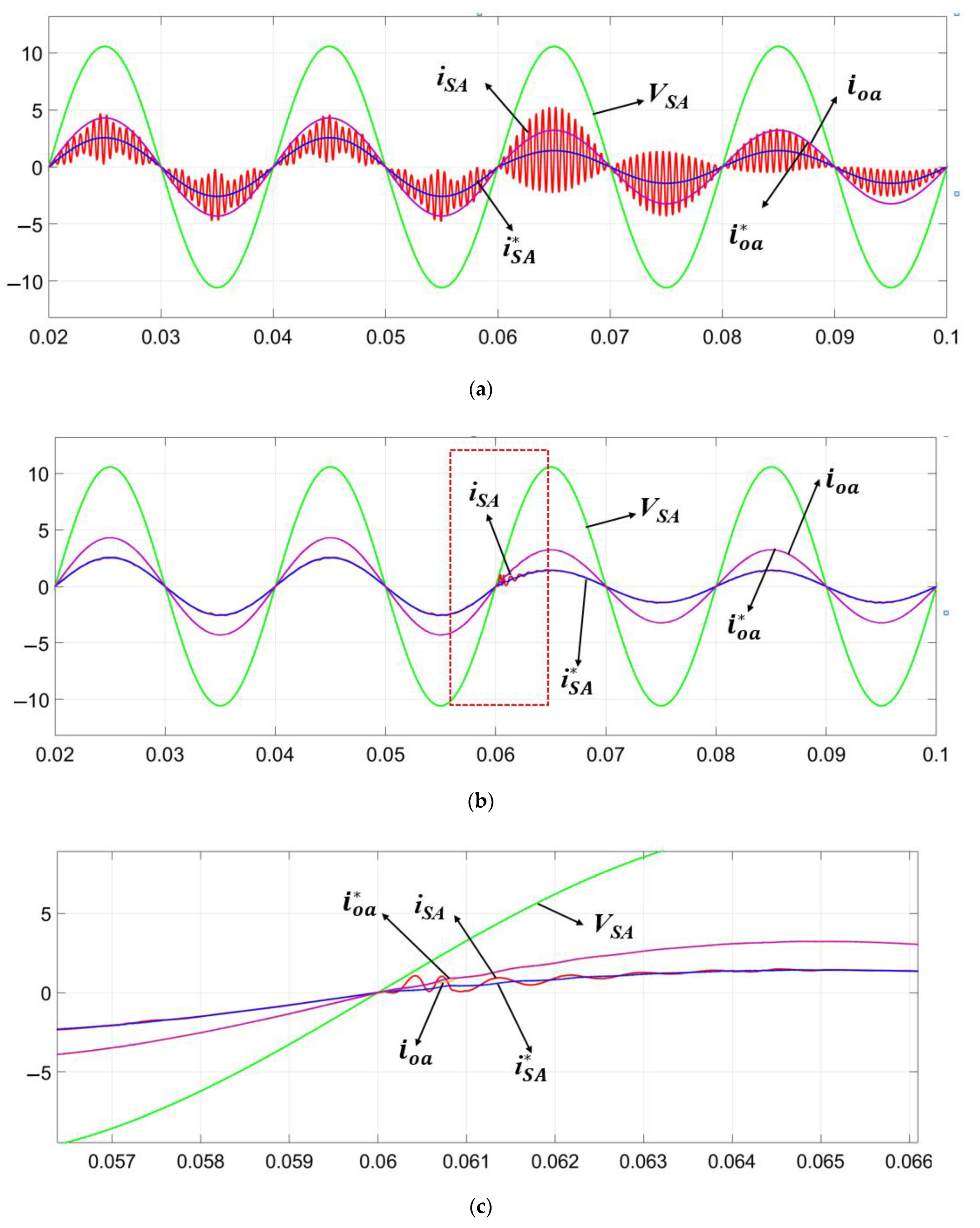
To assess the dynamic performance of the proposed strategy for the TSMC with the IFRS, two groups of simulation results are shown in
Figure 9 and
Figure 10, considering the conditions with the IFRS and without the IFRS. In
Figure 9, the output-current frequency steps from 25 Hz to 50 Hz at t = 0.06 s, and the other control parameters remain the same. In
Figure 10, the output-current reference amplitude steps from 4.3 A to 2.15 A at t = 0.06 s, and the other control parameters remain the same. As illustrated in
Figure 9 and
Figure 10, the system resumes quickly after minute oscillations in a short time, when the output-current frequency or the output-current reference amplitude steps at t = 0.06 s. At the same time, almost sinusoidal waveforms of the source current and output current can be reached with a very good tracking to their references with the IFRS, and the source current is always in phase with the source voltage with the source reactive power minimization in both cases of output-current reference and output-current frequency changes. As expected, the control scheme presents a fast dynamic response on both the input and output sides.
5. Experimental Results
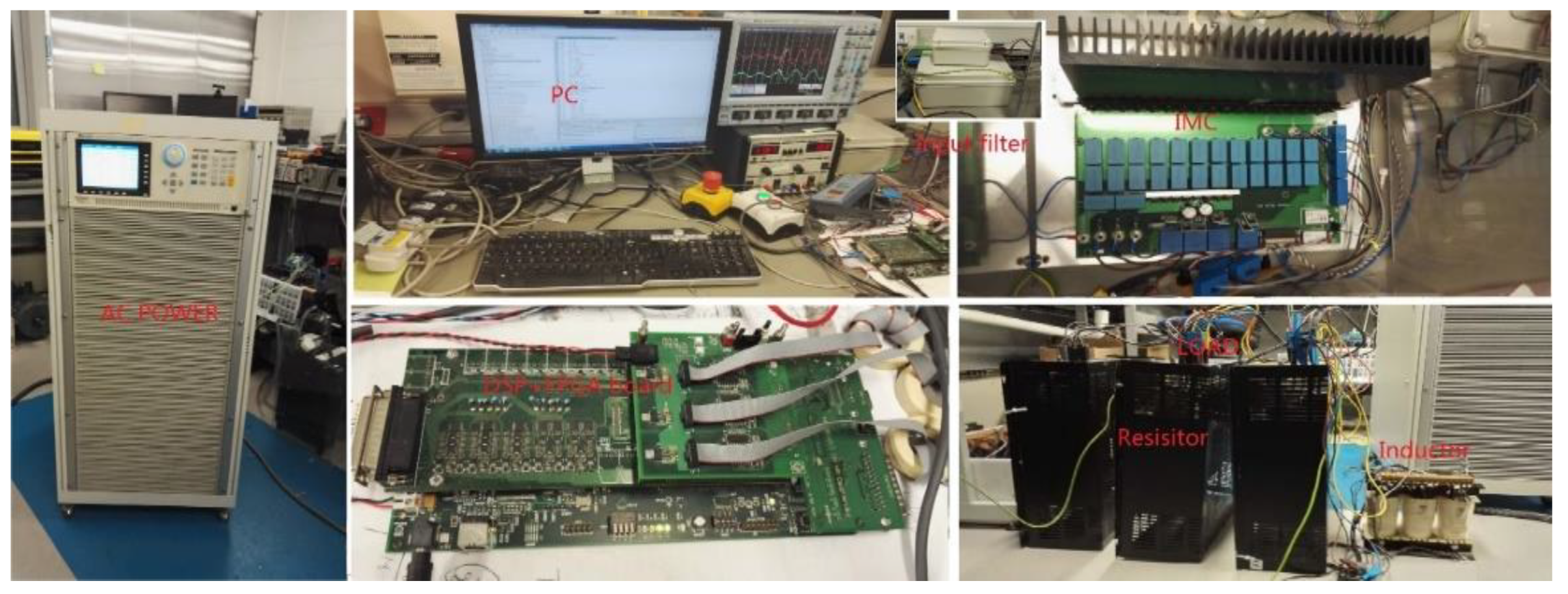
A laboratory TSMC prototype designed and built by the University of Nottingham for experimental evaluation. The prototype is shown in
Figure 11 and the relevant experimental parameters are shown in
Table 3. The scheme is implemented in a spectrum digital control board integrating a Texas Instruments C6713 DSP and a ProASIC3 FPGA. Compared to the OSMC, the TSMC presents zero current switching for the rectifier and thus, can simplify the commutation of the bidirectional switches in the rectifier. While the inverter stage has no particular commutation schemes with hard switching operations. Owing to this, unlike the OSMC, where all 18 switches have to be realized using Silicon Carbide (SiC) MOSFETs, this experiment used 12 standard insulated gate bipolar transistors (IGBT, IKW15T120) for the rectifier and 6 SiC MOSFETs (C2M0080120D) for the inverter, considering the high switching frequencies and the switching losses. Besides, a radiator is used to dissipate the heat produced by the high-frequency switches. In addition to the input filter, an EMI filter capacitor is connected to the output of the AC source. More details about the EMI filter can found in [
32].
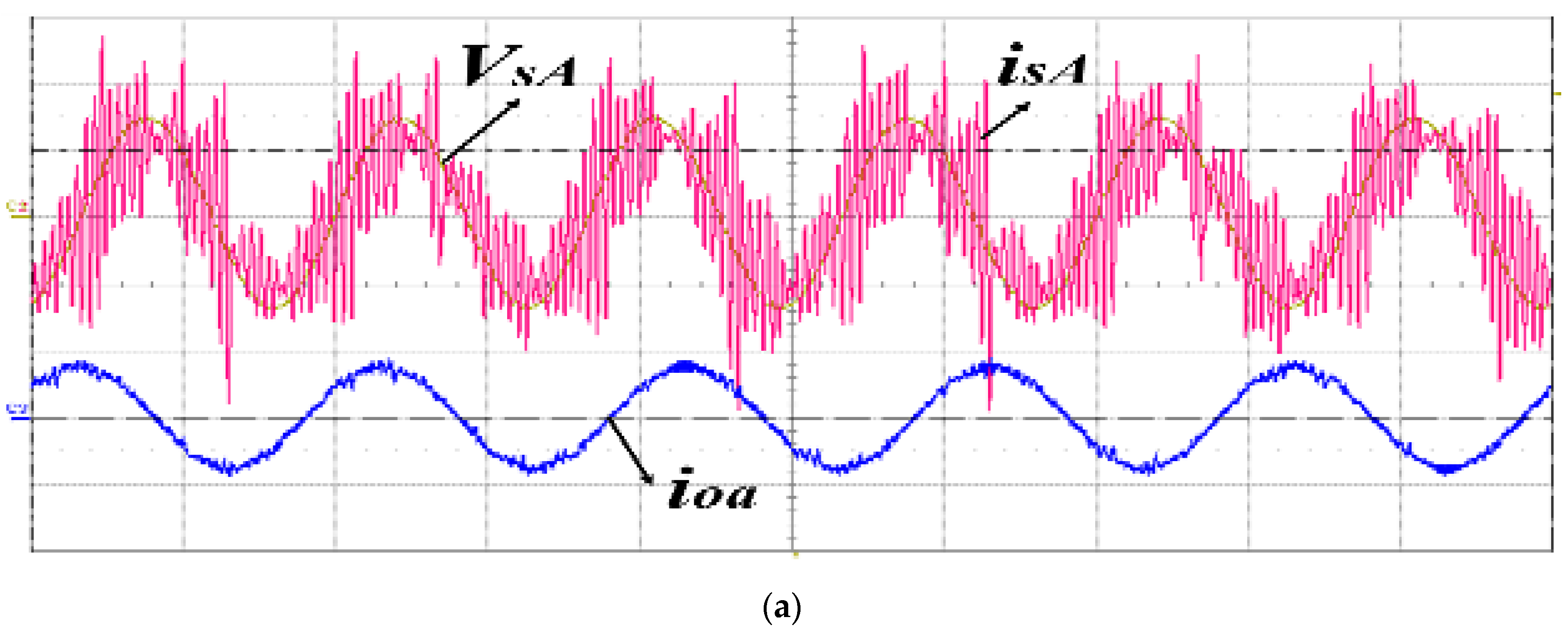
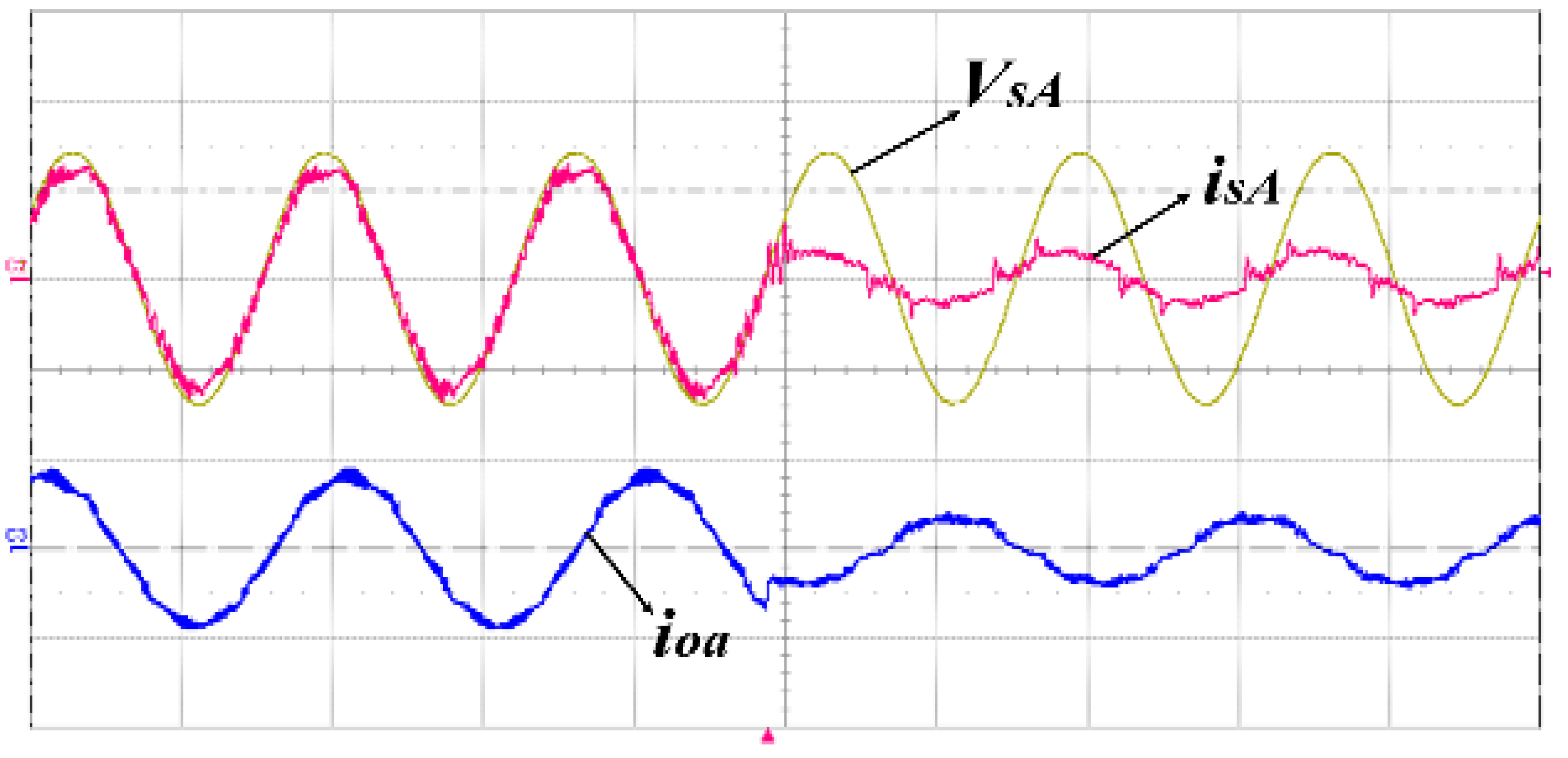
Firstly, the conventional model predictive control strategy for the TSMC without the IFRS and the OSS is implemented, and the results are shown in
Figure 12. From
Figure 12a, the source current is highly distorted with a THD of 92.42%. As seen in
Figure 12b, the main distortions are situated around the input filter resonance frequency calculated based on Equation (51). In addition, the waveforms of the source voltage and the output current are also affected by the large oscillations of
, due to the direct topology of the TSMC. From
Figure 12, it is clear that the input filter resonance is necessary to be suppressed to improve the power-quality performance of the TSMC system.
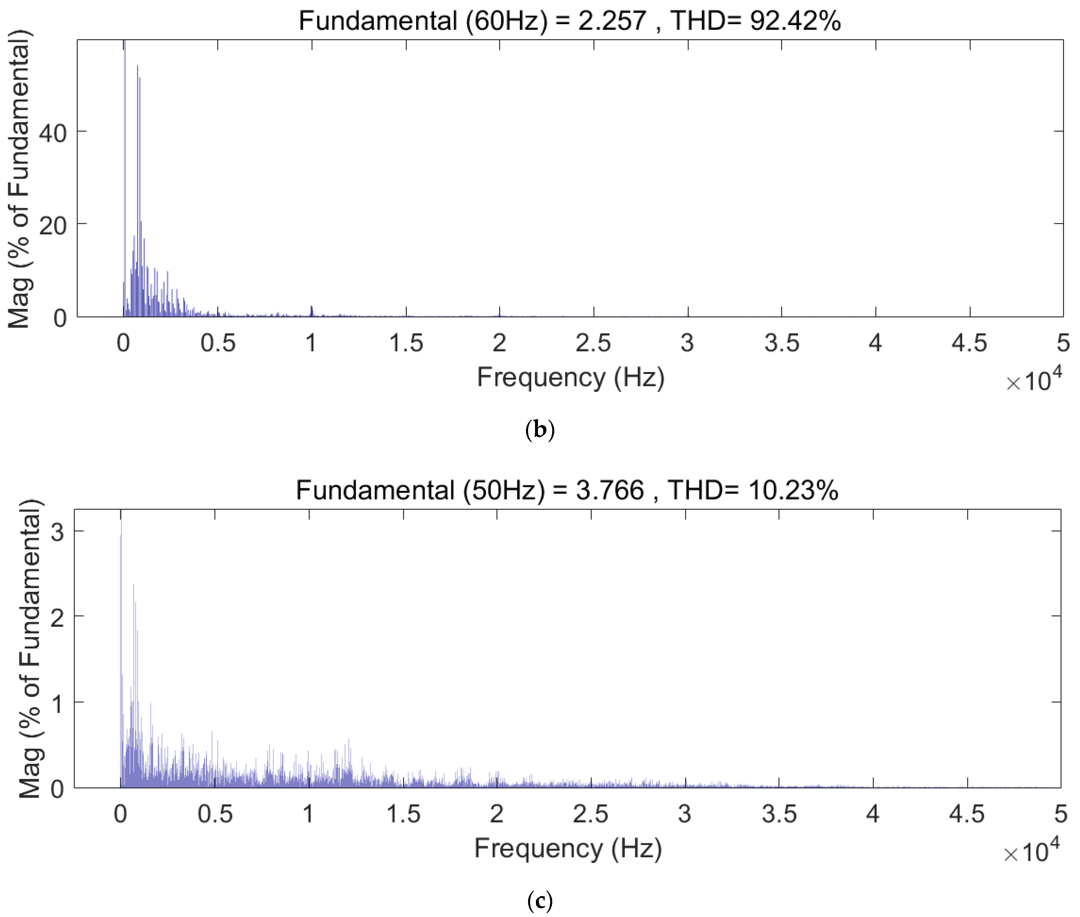
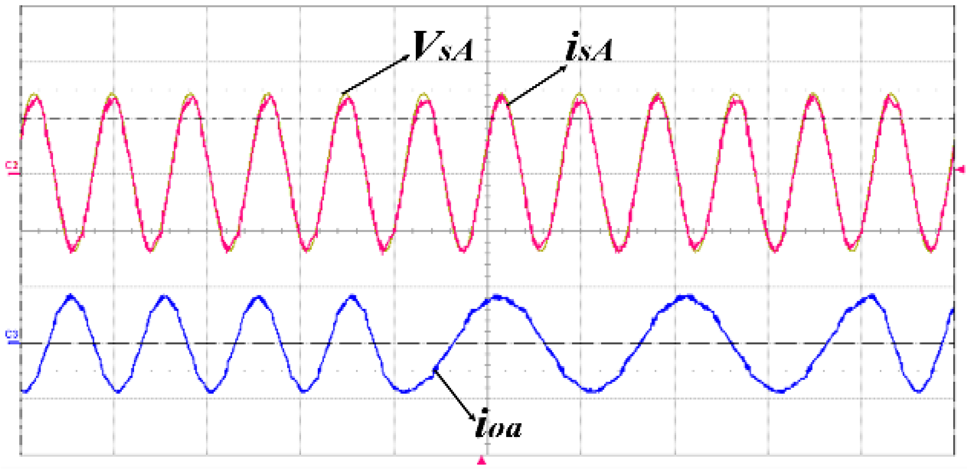
Secondly, the IFRS is added to the CMPC for the TSMC and the results are shown in
Figure 13. Compared with
Figure 12, with the help of the IFRS, the quality of the source current is largely improved with the THD of 11.49%, and the THD of the output current is also improved from 10.23% to 8.25% respectively. From
Figure 13b, the distortions around the input filter resonance frequency are significantly suppressed, the maximum amplitude is under 4%, while the maximum amplitude is over 60% without the IFRS in
Figure 12b. Besides, the variable switching frequency and a broad harmonic spectrum phenomenon can be easily observed in
Figure 13b,c. The source current is not always in phase with the source voltage in
Figure 13a, which indicates that the minimization of the instantaneous source reactive power based on Equations (10) and (30) needs to be improved.
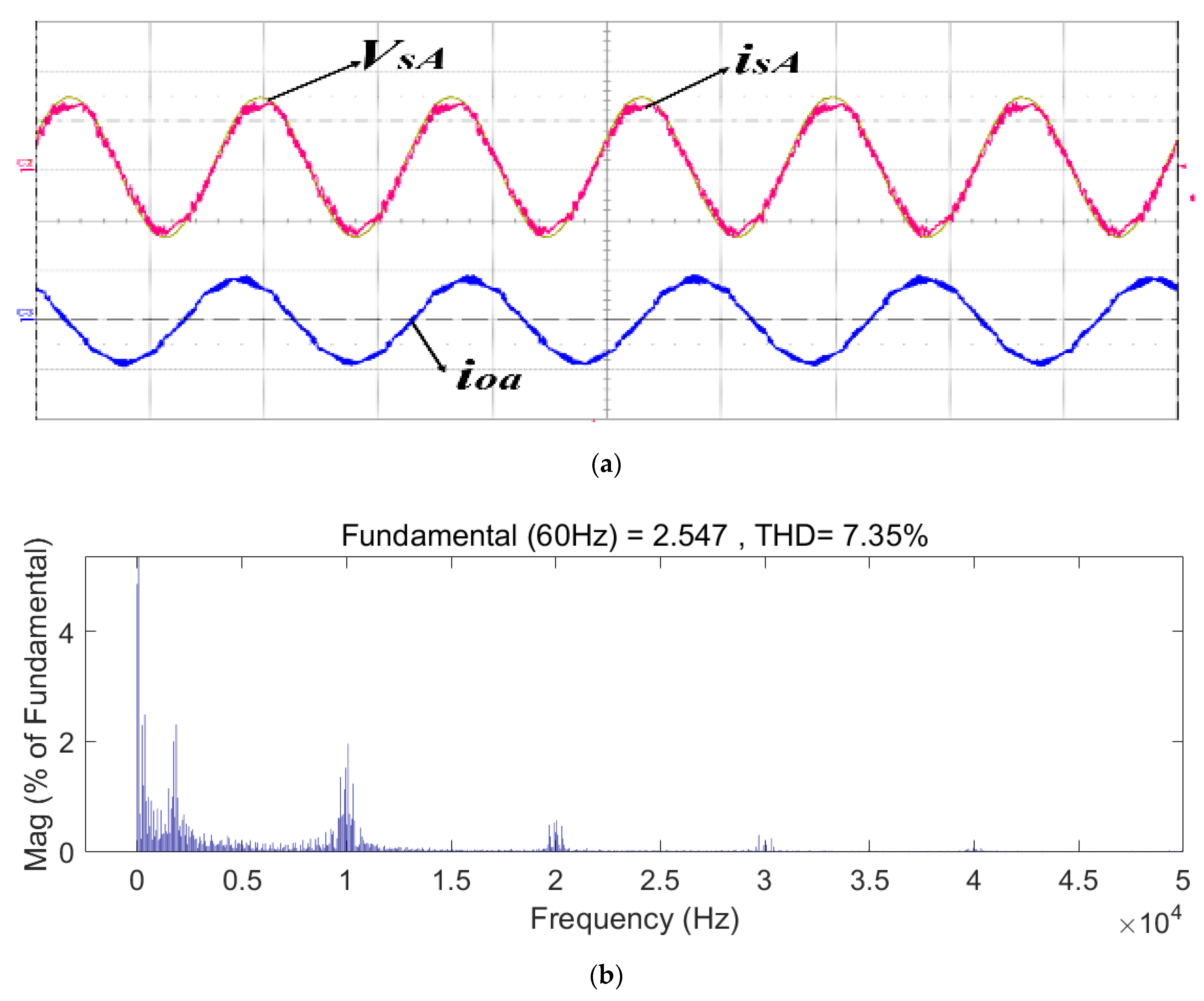
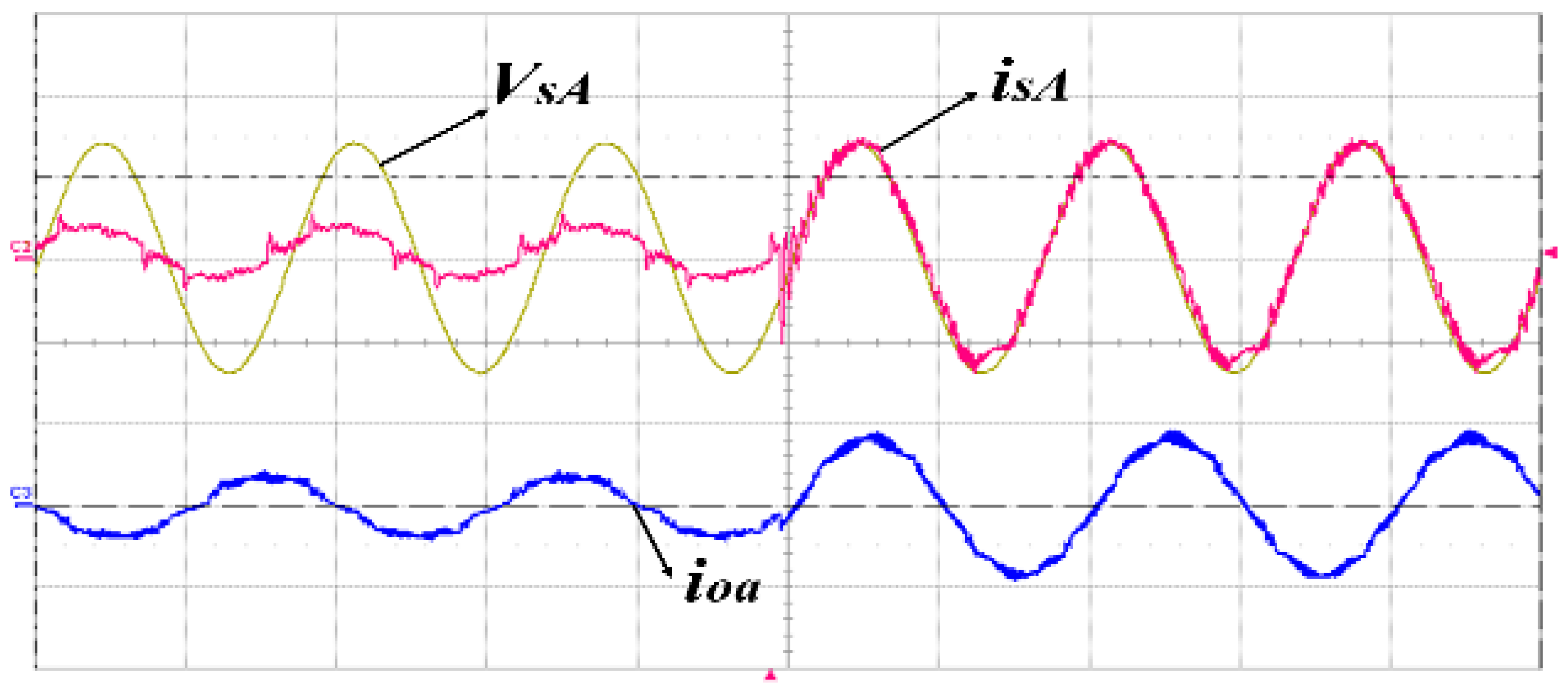
Thirdly, the proposed VMMPC strategy with the IFRS and the OSS for the TSMC is evaluated, and the results are shown in
Figure 14. Compared with
Figure 13, the source current
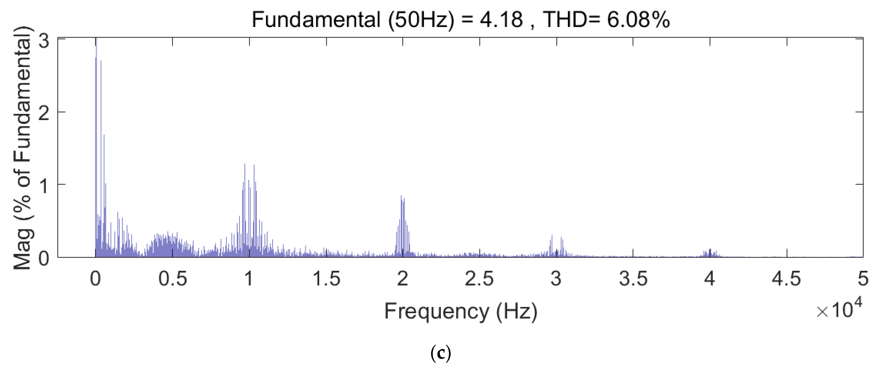
is improved with a THD from 11.49% to 7.35%. From
Figure 14b, the distortions around the input filter resonance frequency are suppressed, the maximum amplitude is near 2% with the proposed VMMPC strategy, while the maximum amplitude is 4% with the CMPC. The THD of the output current is also improved from 8.25% to 6.08% respectively. Besides, from
Figure 14b,c, it is clear that the harmonics are concentrated around the fundamental frequency and its multiples frequency, the fixed switching frequency phenomenon can be easily observed. The source current is always in phase with the source voltage in
Figure 14a, which indicates the minimization of the instantaneous source reactive power based on Equations (10) and (30) is also improved compared with
Figure 13a.
In addition, since the proposed control strategy controls the instantaneous source reactive power on the input side, the parameter named as the mean power
is defined to assess the performance:
where
is the actual value of power at the
kth sampling instant and
m is set to 10,000.
The comparisons between the CMPC and the proposed VMMPC with the OSS are shown in
Table 4.
From
Table 4, the proposed VMMPC with the OSS can obtain better performance in all aspects of the instantaneous source reactive power, the source current, and the output current, compared with the CMPC.
It should be stated that the CMPC may obtain a similar performance with the VMMPC in aspects of control objectives, by using a much higher sampling frequency than that in the VMMPC [
18,
22]. However, since predictive controllers are commonly demanding in terms of computational resources, it is not always possible to increase the sampling frequency in practical implementations. Besides, the variable switching frequency with the CMPC is a lurking peril for the control system [
18].
Besides, the amplitude of the output current is 4.18 A, thus there exists a 2.8% steady-state error, because the reference of the output current is set to 4.3 A. In fact, a steady-state error between the measured current and its reference is normal in model-based control strategies, where a steady-state error on the controlled variables usually occurs from the system model inaccuracies. This can be usually compensated by external control loops (e.g., PI controller-based). Besides, in [
33], a method aiming to improve the system parameter robustness with the CMPC has been proposed, which can also mitigate this problem.
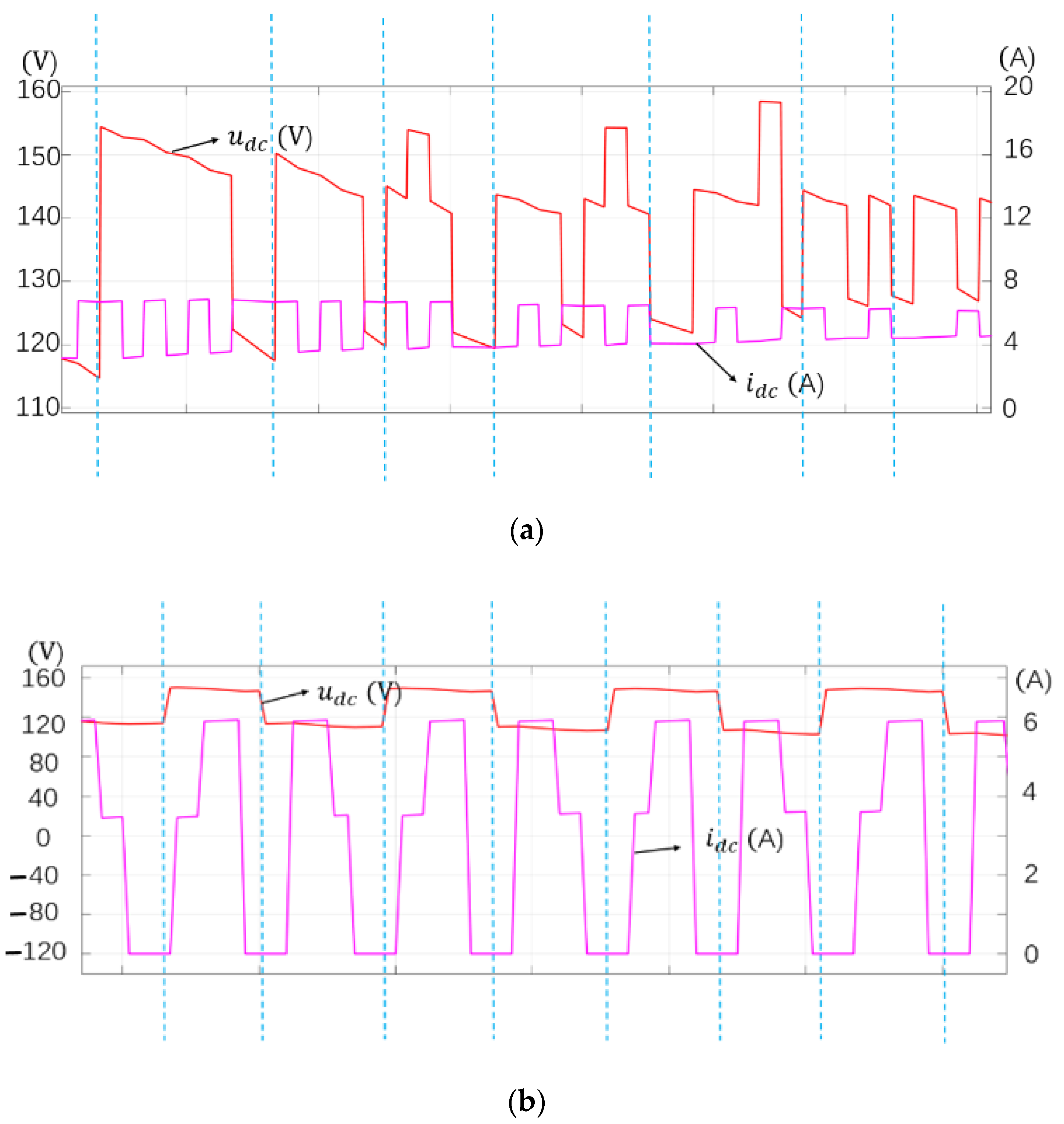
Furthermore, the waveforms of the dc-link voltage
and current
with the CMPC and the VMMPC with the OSS are shown in
Figure 15. The commutation of
represents the switching state change of the rectifier stage. From
Figure 15a, it is possible to change the switching state of the rectifier stage when
is nonzero (blue line). This may increase the converter switching losses and require a more complex commutation strategy (e.g., four-step commutation) for the rectifier stage. On the contrary, in
Figure 15b with the proposed control strategy, the commutation of
always occurs when
is zero (blue line), which guarantees the zero-current switching of the rectifier stage.
Finally, transient results are shown in
Figure 16,
Figure 17,
Figure 18 and
Figure 19. The output-current frequency reference is changed between 25 Hz and 50 Hz in
Figure 16 and
Figure 17, and its amplitude reference is changed between 2.15 A and 4.3 A in
Figure 18 and
Figure 19. As indicated in
Figure 16,
Figure 17,
Figure 18 and
Figure 19, almost sinusoidal waveforms of the source current and the output current are obtained, and the output current shows a good tracking to the reference. Besides, the source current is in phase with the source voltage, achieving the minimization of the instantaneous source reactive power, and the source and output currents show fast dynamic responses to the variations of the references. As expected, the proposed strategy demonstrates a fast dynamic response and a good performance in the transient state.
6. Conclusions
For matrix converters, an input filter is necessary for the commutation of switching devices and to mitigate against line-current harmonics. However, the filter configuration presents a resonance frequency and can be excited by the utility due to the potential fifth and seventh harmonics in the ac source (series resonance), and also by the converter itself (parallel resonance). Besides, the model predictive control strategy is more likely to excite the input filter resonance, when compared with traditional control methods, leading to additional harmonics in the AC source and distorted source current waveforms.
To solve these problems above, a vector modulation-based model predictive control strategy is proposed, which controls the source reactive power and the output currents with fixed switching frequency. The advantage of the proposed VMMPC strategy compared with the CMPC is firstly proven using the principle of vector synthesis and the law of sines in the vector distribution area. Besides, an optimal switching sequence is proposed, which can guarantee safe zero-current switching operations and reduce the switching losses. This pattern can simplify the commutation of TSMC and avoid complex commutation strategies (e.g., four-step commutation) in traditional control methods. Furthermore, a novel input filter resonance suppression method is proposed and implemented in the VMMPC for the TSMC, which shows good damping performance and easy implementation. In fact, the IFRS method proposed in this paper is not only suitable for the TSMC with the MPC scheme but also can be used for other power converters, i.e., current source rectifiers and inverters and other control techniques, i.e., the space vector pulse width modulation technique, where the reference amplitude of the load current or voltage can be modified.
Experimental results validate the performance of the proposed method, which features unity input displacement power factor, low source-current distortions, good sinusoidal waveforms of output currents, and zero-current switching operations, demonstrating that the proposed control technique poses an attractive alternative to classical control strategies for the TSMC.


