1. Introduction
The rapidly increasing share of semiconductor switches in electrical engineering is due to their high performances in terms of controllability, compactness and lifetime. This can be seen in many domains such as power electronics, motor drivers and many other areas, including pulsed power.
In pulsed power field, semiconductor switches can be used to build powerful capacitors charger for Classical Marx generators such as in [
1,
2]; or to design the pulse itself by substituting classical switches such as spark-gaps by semiconductor switches.
Currently, pulse power generators based on semiconductor switches can be classified into two main groups. The first one gathers generators using specially designed switches such as Semiconductor Opening Switch (SOS) [
3,
4,
5,
6], Drift Step Recovery Diodes (DSRDs) [
7,
8] and other similar devices [
9,
10,
11]. These generators provide very high performance because their architectures are optimized and specially designed for pulsed power generation. However, the discussed switches are pretty rare, if available on the market at all, and their cost is also too high.
The second group of generators uses commercial (off the shelf) components such as (silicon) IGBTs and MOSFETs. These switches are widely available and show generally lower cost. A significant number of works proposing various structures of pulsed power generators [
12,
13,
14,
15] using this type of switches can be found for different applications. Increasing interest in these designs is motivated by the continuous progress in their power range and, especially switching times especially after the development of the new technologies such as SiC [
16] and GaN [
17] devices. This increases considerably the power range and also the robustness of the switch. However, even though there is continuous progress in the performance of these devices [
18] and their gate driving circuits [
19], they still suffer a major problem: their limited power capabilities in particular voltage ratings.
There are three possible solutions to this problem: the first is to develop new devices with higher power capabilities [
20,
21,
22,
23]. This option is challenging due to physical limitations and the resulted dramatic cost increase. The second solution is to combine many devices in series and in parallel to create more powerful switches [
24,
25]. However, this also has some difficulties connected with the way to distribute equally the power across all the devices. The second problem is when one of the components fails, the probability of the others to fail increases exponentially what causes the failure of the whole device. The third possible solution is to use a modular structure generator [
26,
27] using “low rate” components. This approach seems to be more suitable comparing to the previous solutions because it ensures equal power distribution on all switches. Moreover, the number of stages can be adjusted to increase or decrease the maximally allowed voltage. In case of failure of one stage, the other stages can be protected.
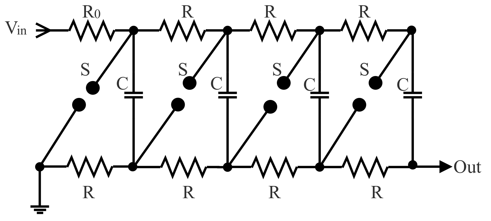
Therefore, a new high voltage pulse generator with a modular structure and off the shelf components is presented in this paper. A special interest was in testing the performance and the robustness of the SiC technology in pulse power. For that purpose, a new modular architecture of a high voltage pulse generator based on the classical Marx structure (
Figure 1) is proposed. The design and the concept of the generator are presented to discuss its strengths and weaknesses.
The designed generator is aimed to be used in biomedical applications such as nsPEF electroporation tests. Due to the high controllability of the generator, it is possible to check precisely the effects of different parameters such as applied field amplitude, pulse width and repetition rate, on the efficiency of the electroporation process.
In this process, living cells are treated with intense nanosecond Pulsed Electrical Field (nsPEF) created by applying the generated voltage pulses to a special electroporation cuvette. It consists of two separated conductive armatures (generally, the distance between them is 1, 2 or 4 mm). Cells under testes are kept in a special solution called MEM (Minimum Essential Medium) which has quite high conductivity due to its high contents of salts. A special technique for the estimation of the conductivity of the MEM in pulsed mode is presented in [
28]. Thus the cuvette impedance varies from some ohms to hundreds of ohms depending on the used liquid, the tested volume, and the cuvette dimensions. Other works on the estimation of electromagnetic properties of human tissue can be found in [
29].
In the next two sections, the structure and the operation principle of the proposed generator are described with some advanced theoretical analysis such as the extreme performance and the power efficiency of the generator. Then, the third section presents a more detailed, computer simulation of the proposed structure. Finally, in
Section 5, the results of the experimental tests with the five-stage prototype generator are presented.
2. Principle of Operation
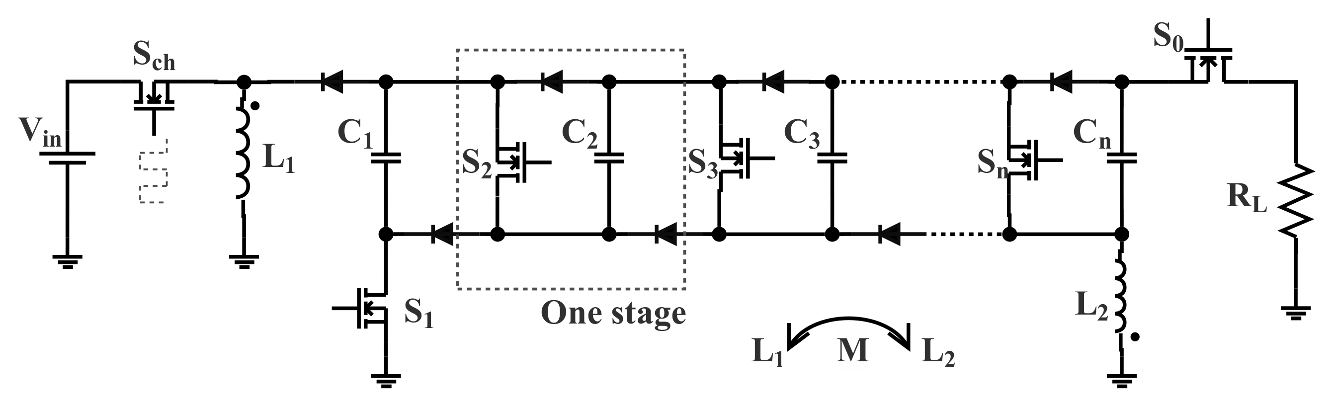
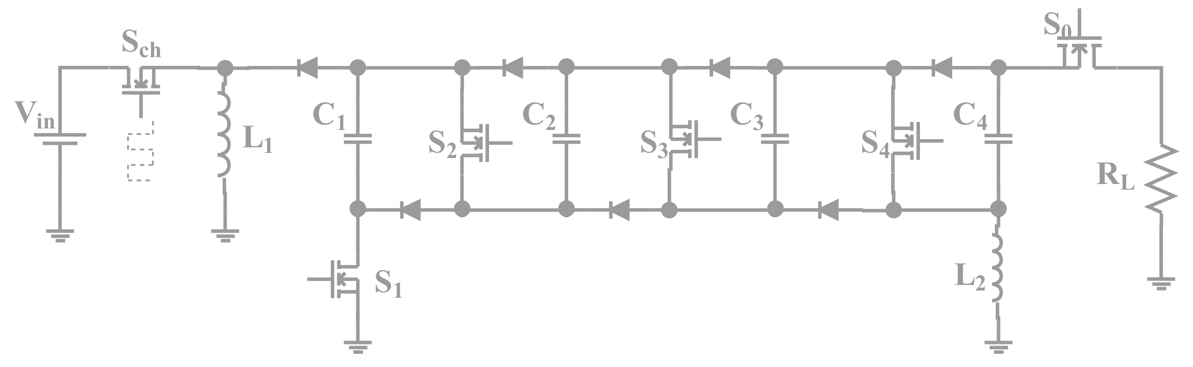
The proposed architecture, shown in
Figure 2, is based on the negative structure of Marx generator (see
Figure 1) with some changes. The spark gaps were substituted by SiC-MOSFETs and the charging resistors by diodes. However, unlike the usual structure of solid-state Marx generators, which uses resistors [
21] or an inductor [
30] to charge the capacitors, in the proposed design, charging is done via two magnetically coupled inductors
and
. The first is connected to the power supply side and the second to the load side as shown in
Figure 2. A charging switch
is also used to exploits the boost effect to get a controlled high voltage charging from a low DC voltage supply.
The proposed structure can be seen as a special combination of a solid-state Marx generator with an inverting DC-DC boost converter. The idea of using two coupled coils (i.e., split the inductance of the inverting converter in two coupled parts) allowed us to reduce the number of controlled switches to half compared to [
31], Which reduces considerably the size, cost and complexity of the system.
Similarly to the generator presented in [
30], the second coil
plays two main roles. The first is to provide a path for current charging capacitors independently of the load. The second task is to block the current in the discharge phase, because for fast and short pulses the coil can be treated as an open circuit and its impedance will be very high compared to the load impedance.
Using this configuration, the capacitors are charged negatively with respect to the input, which means that the output pulse has also a negative polarity. The charging system ensures the controllability of the output pulse amplitude, moreover, the charging voltage can be many times higher than the input one due to the boost factor of the charging circuit multiplied by the Marx’s number of stages, which ensures a high voltage gain. Additionally, the charging process is not affected by the load in any way, which solves the problem of the influence of the load on the pulse amplitude and charging time spotted in many designs [
21,
32].
As mentioned before, this structure can be seen as an inverting DC-DC supply connected to a classical solid-state Marx with semiconductor switches. This class of generators was the subject of many studies, such as [
30], However, these solutions did not exploit to the maximum the capabilities of the combination inverting DC-DC boost converter with solid-state Marx generator. A comparative study will be presented later in
Table 1 to highlight the pros and cons of the proposed structure compared to previous ones found in the literature.
The used semiconductor switches enable efficient control of the repetition rate and the output pulse width. This means that the generator provides full control over the generated pulses, an essential requirement in biological and medical applications.
From numerous types of semiconductor switches, the choice of SiC-MOSFET was done for several reasons. The first is the switching time, which is very short comparing to similar switches such as IGBTs. Moreover, comparing to classical MOSFETs, SiC ones have similar switching time but better power capabilities, in particular, the rated voltage and its high robustness against current peaks. This makes them a good compromise between IGBTs and MOSFETs with acceptable power range and fast switching.
The generator operates over three main phases. The first is charging the capacitors. This phase runs over two steps: charging the inductors, then transferring the energy to the capacitors. These two steps are repeated many times until the full charging of the capacitors. The second phase is a steady-state, in which the system waits until the firing signal arrives to trigger the third phase—a discharge. The next paragraphs discuss these three phases in details.
2.1. The First Phase—Charging of the Capacitors
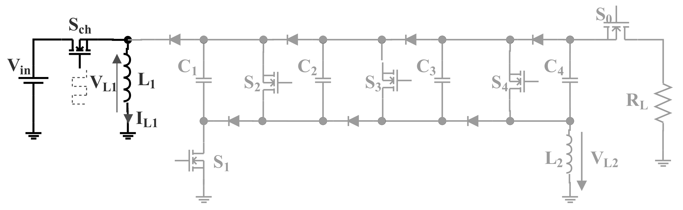
We shall start the description from the moment when the capacitors are discharged or partially charged with a voltage
, all the
switches and all diodes are opened. When the switch
closes, the current flows from the DC supply through
. The equivalent circuit of the generator is shown in
Figure 3. It consists of a DC supply in series with an inductor. The inductor starts to store energy as a magnetic flux within the magnetic core.
When
opens, all the diodes start to conduct and the current passes via
and
, charging all capacitors simultaneously in parallel (see
Figure 4). As the two inductors are magnetically coupled, in other words, they share the same flux, the current can be shared between them in a way that they conserve the total stored energy. The condition
, where
and
are the
currents exactly before and after opening
, must be full-filled. If the two inductors are identical
, then
. It should be mentioned that if the two inductors are not coupled, then charging the capacitors cannot be done, as the current through
cannot jump from 0 to
instantaneously.
If
is controlled using a fixed frequency PWM signal with a duty cycle
D, then, the whole generator is equivalent to the negative structure of the inverting DC-DC boost converter. In this case, it is proven that the charging voltage of the capacitors
is given by Equation (
1)
This equation can be used to calculate the proper duty cycle to obtain the desired charging voltage (an open-loop control technique). However, due to leakage currents and the non-perfect coupling between the two coils, a closed-loop control technique shows better performance. Measuring the voltage across one capacitor and compare it to the required value is needed. Any control technique, such as proportional-integral-derivative controller (PID), can be applied to ensure the regulation of the charging voltage to the desired value.
2.2. The Second Phase—Waiting Phase
When the voltage across all capacitors equals the required value
remains off and all the other switches and diodes are opened (
Figure 5). The system is ready to fire and waiting for the trigger signal.
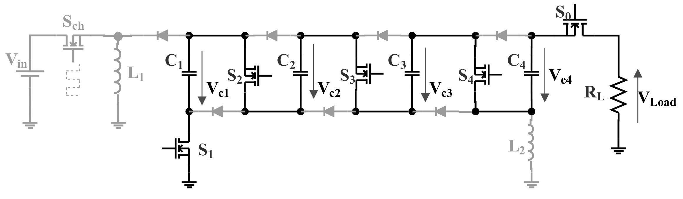
2.3. The Third Phase—Discharge of the Capacitors
When the trigger signal arrives, all
close simultaneously. This rearranges the capacitors and connects them in series as shown in
Figure 6. The output voltage across the load is given by
. This phase ends by opening
.
When are closed, the capacitors discharge through the load. This decreases the voltage across each capacitor and thus the output voltage also decreases. However, if the pulse width is small comparing to the circuit constant , then the voltage drop is small compared to the pulse amplitude. The final pulse shape can be considered rectangular.
3. Theoretical Analysis
It is imperatively important to understand that the generator operates using two different controlling signals: the first controls the charging voltage of the capacitors by acting on , in other words, it controls the amplitude of the generated pulses. The second signal controls the firing of the generator by acting on all the simultaneously. This controls the repetition rate and the pulse-width.
The frequency of the first control signal (acting on ) can be selected depending on the used switch to be in the range of 10 s of kHz. A good choice of this parameter is very important to facilitate the design of the coupled inductors. This is because the charging current fluctuation is a function of the PWM frequency and the inductance of the two coils and . This can be seen just by considering the whole generator as an inverting DC-DC boost converter during the charging phase.
We should mention that, for repetitive operating, the first charging of the capacitors (initially discharged) takes a longueur time than recharging it after firing the generator (capacitors are partially charged). This can be understood because, to get a quasi-rectangular pulse, we should cut the pulse before the full discharge of capacitors. So recharging them requires less time. Thus, the generator should wait until the full recharging of the capacitors, otherwise, the generated pulses will have a reduced amplitude.
Another point is that the firing of the generator should occur when the system is in its steady-state. in other words, is off and all currents are nullified. This protects the power supply and ensures that the generator fires in its best conditions.
In this way, each parameter of the pulse: amplitude, pulse-width and repetition rate is completely controllable and independent from other parameters and also not influenced by the load. They are just a function of the control signals. However, each parameter has some limits, on beyond them, this independence cannot be preserved.
3.1. Maximal Performance of the Generator
From the previous analysis, it is understood that the proposed structure, as any other one, has some limitation. Some of them are connected to the structure itself and others connected with the limitation of used components. For instance, in theory, the maximal value of the output pulse amplitude is infinite, however, in practice, it is limited by the voltage rating of the used components especially capacitors and switches.
In the case of the pulse-width, its maximal value
is determined by the maximally tolerated droop in the output pulse voltage denoted
. This last one is a function of the RC circuit time constant and the (total capacitance of the generator
and the load resistance
). It is known that the discharge of a capacitor in a resistive load follows an exponential law, Thus, we can use it to prove that the maximal pulse-width is given by Formula (
2). On the other hand, the minimal pulse-width
is limited by the sum of the switches rise and fall time.
The maximal repetition rate
is also limited. The main constraint is the capacitors’ recharging time, which is a function of the maximal charging current
, the total capacitance of the generator
and the voltage droop of the output pulse
. The maximal repetition rate can be evaluated using the following formula:
3.2. Power Efficiency
The classical way of charging the capacitors is by using charging resistors. In this way, the half of consumed energy is stored in the capacitors and the other half is dissipated in the resistor as joule losses. Thus the power efficiency of the generator cannot exceed 50%.
That’s why the charging process in the proposed structure is resistance free. This means that almost all the energy can be transferred to the capacitors. This means that power efficiency can reach 100% in theory. Nevertheless, in practice, there are still some losses caused mainly by:
Internal resistance of coils and and the other components;
Switching losses in the SiC MOSFETs and diodes;
Magnetic losses in the magnetic core between and ;
The main power losses in the generator occur during the charging phase, during which the system can be considered as an inverting DC-DC converter. Generally, the power efficiency of a inverting converter is inversely proportional to the absorbed power. Thus if charging power increases by increasing the amplitude, the repetition rate or the pulse-width of the generated pulses, the power efficiency decreases.
4. Simulation
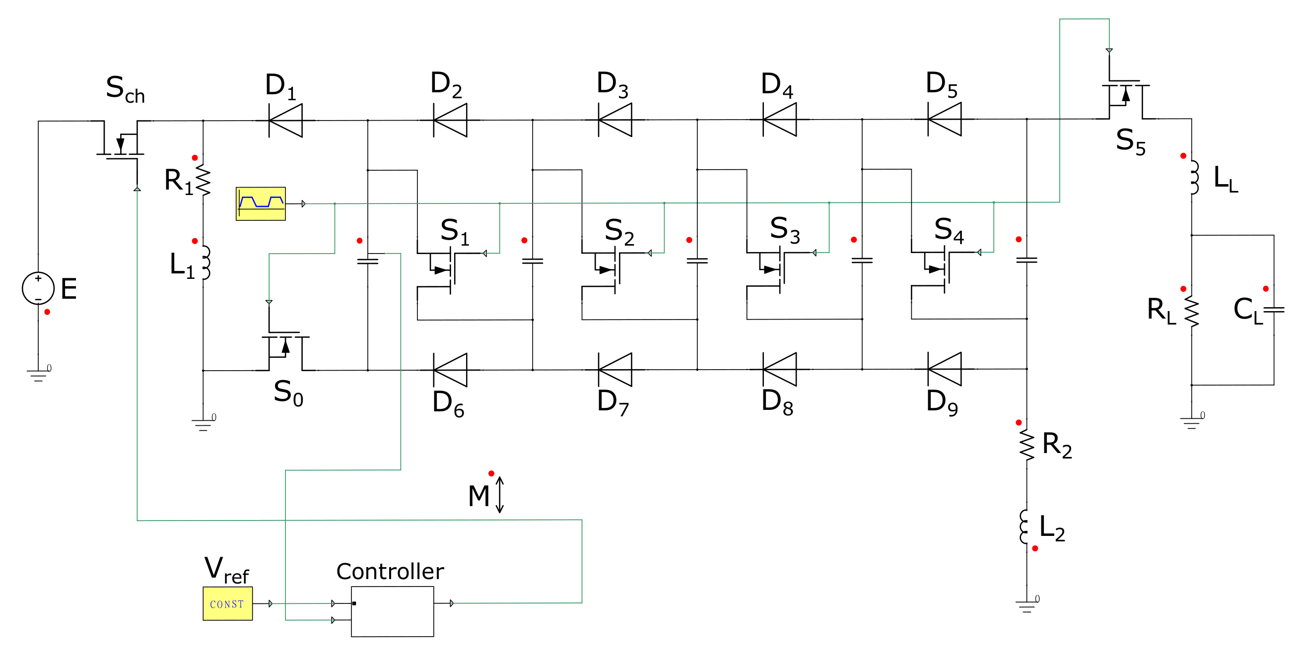
In order to validate the previous functioning principle, a numerical simulation was elaborated using ANSYS-Simplorer as shown in
Figure 7. The model uses the following parameters:
The voltage regulation was performed using a sliding mode controller (SMC). This technique consisted of applying the Maximum Duty Cycle when the capacitor’s voltage was smaller than the reference value and stopping when it was higher. This control technique is very popular in power electronics due to its simplicity and robustness. A smooth transition between the two states was inserted to eliminate the shattering.
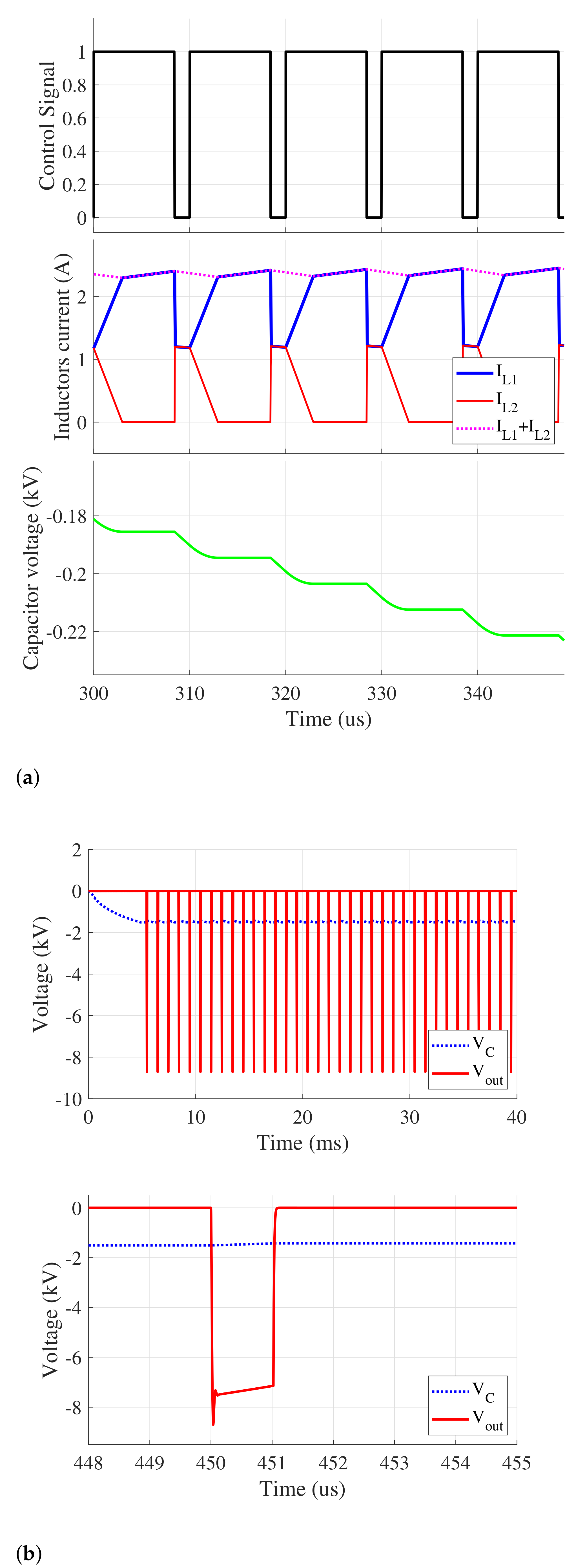
The obtained results are presented in
Figure 8a,b. The first figure presents the signals during the charging phase. From top to bottom: the control signal of
, the two inductors’ currents and then the voltage across one of the capacitors. The second figure shows the output pulses compared to the voltage across one capacitor.
From the currents’ waveforms, it can be noticed that current was always continuous, which reflected the conservation of the magnetic flux even if the currents in both inductors (blue and red respectively) were not continuous. The last waveform shows that the voltage across capacitors rose regularly every period for a constant charging current.
Figure 8b shows the voltage across one capacitor and the single output pulse. The input voltage used in this simulation was 25 V with the charging voltage reference fixed at 1700 V. It can be seen that the output pulse was almost four times the charging voltage and the pulse shape was indeed quasi-rectangular. The total voltage gain in this case was around 80.
The power efficiency of the generator was estimated for different values of the pulse-width between 100 ns and 3 us, for an amplitude of 2 kV and a repetition rate of 1 kpps. The obtained results are presented in
Figure 9. For short pulses, the power efficiency seemed to be not influenced by the pulse-width variations. However, when the pulses got longer, the power efficiency decreased rapidly. This can be explained because longer pulses meant more voltage droop and higher discharge of the capacitors. In other words, more power was needed to recharge them again and more power losses too.
5. Experimental Results
In order to check the functioning principle and the validity of the simulated model and results, a five-stage generator, shown in
Figure 10a, was designed and tested within the High Voltage Laboratory at Warsaw University of Technology. Each stage consisted of a 100 nF SMD ceramic capacitor that can withstand 2.2 kV, fast recovery diodes DH20-18A with a blocking voltage of 1.8 kV and a 1.7 kV SiC-MOSFET. Hence, the maximal possible pulse amplitude was −8.5 kV.
The chosen SiC-MOSFET, SCT2750NYTB from ROHM Semiconductor company, had an internal resistance of 750 mΩ during the on-state. It could handle a drain pulsed current of 14A. The choice of this switch was a compromise between performance which was dictated by the application and the price. As discussed before, the generator was designed to be used for biomedical application where the load impedance varied hundreds of ohms to some kilo-ohms. Hence the choice of this device for a five stages generator and a typical load of 500 Ω is reasonable.
Regarding the two coupled inductors design, the high voltage stress applied to during the discharging phase, together with the resulting potential difference between and and the parasite capacitance (inter-spires and inter-coils) made their conception challenging. Thus a well-studied design accompanied with a delicate implementation was unavoidable.
The results presented in Figure a–f were obtained using different loads from 200 Ω to 1 kΩ, and an input voltage of 24 V. The whole system was controlled using a DE10-lite FPGA board—all the signals (control and feedback) were transmitted between the generator and the control unit using optical links. This ensured high insulation and protects the FPGA from any perturbation caused by the generator discharges. The signals were recorded using Keysight DSOX3054T oscilloscope with a maximal sampling rate of 5 GS/s and a Tektronix P5100A probe of a 1 kV.
On the left inset,
Figure 10b presents the output pulse of the generator. The pulse had effectively a clear quasi-rectangular shape with a pulse-width of 0.5 μs. The amplitude of the pulse was regulated to be 1 kV, which was 40 times higher than the input voltage although the generator contains just five stages. This is owed to the boost effect discussed before in
Section 2. From the same figure, the pulse also showed a small voltage drop caused by the partial discharge of the capacitors within the load.
A zoom of the first edge of the pulse as shown in
Figure 10c allows us to assess that the rise-time was around 8 ns (dv/dt > 125 kV/μs). This value was a function of the maximal blocked voltage and current to be reached. Therefore it can be deduced that the rise-time was a function of the pulse amplitude and the load impedance. Additionally, it was significantly influenced by the MOSFET’s gate driving technique, and the generator structure (in other words the total inductance of the generator).
Additional tests were performed to check the controllability of the generator in terms of amplitude, repetition rate, and the pulse-width. The influence of the load on the final pulse shape was also investigated. The results are presented in
Figure 10d,f.
Figure 10d shows five overlapped pulses with the same 500 ns pulse width and different amplitudes. The adjustment of the amplitude was done by acting on the charging voltage which is controlled by acting on
as we previously explained. The pulses were recorded using 1 kΩ load. It can be observed that pulses had similar shapes, moreover, as mentioned before, that the rise-time was increasing with the amplitude. From these results, it can be concluded that dv/dt was almost constant.
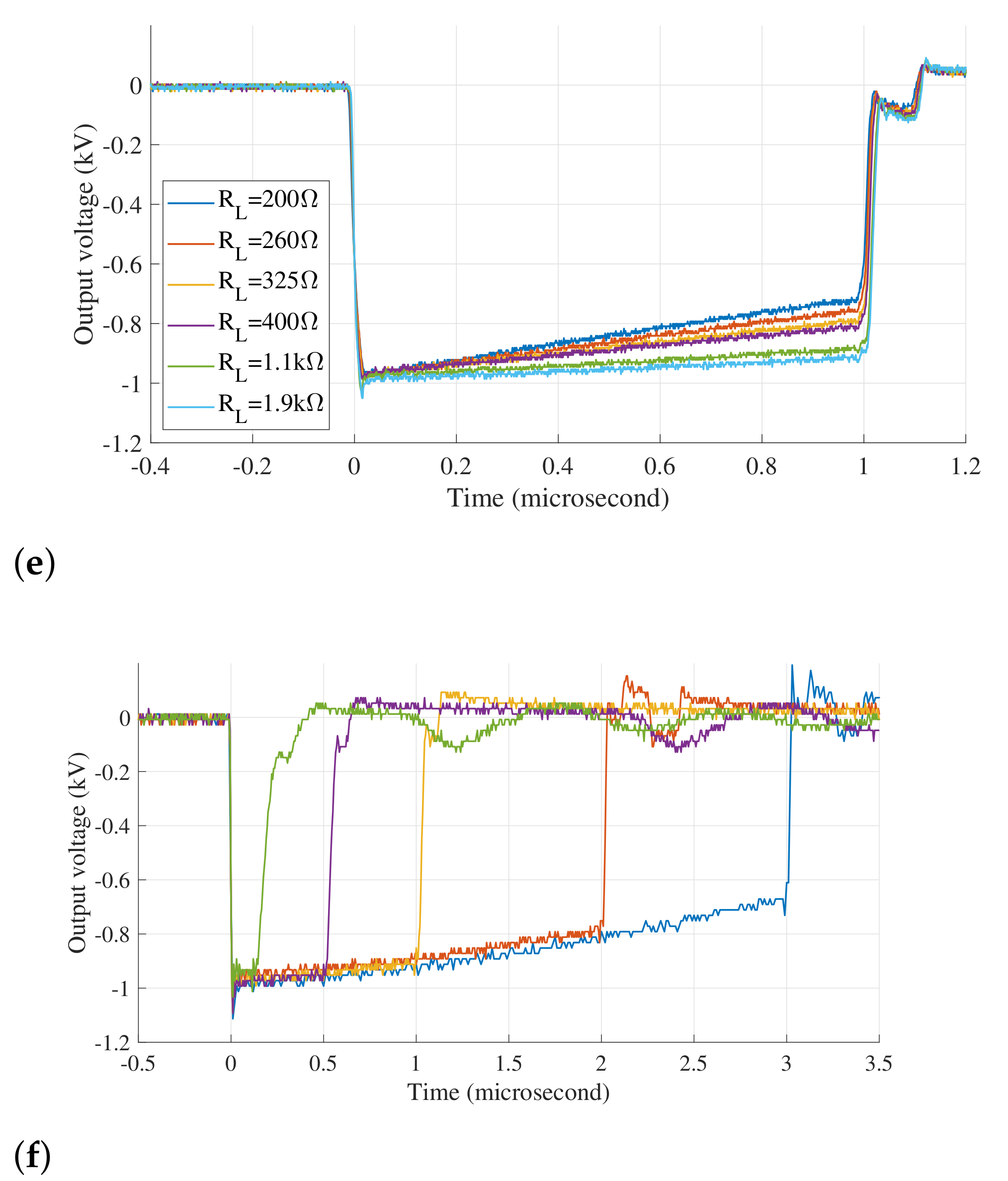
Next,
Figure 10e shows the output pulse waveform with a width of 1 μs and an amplitude of 1 kV for different loads in the range of 200 Ω to 1.9 kΩ. For this pulse width, the voltage drop was 25% for minimum load and less than 5% for maximum load. This did not significantly affect the rectangular shape of the pulse. It may be mentioned that this drop was smaller for shorter pulses.
On the
Figure 10f five overlapped pulses are presented with 0.1 μs, 0.5 μs, 1 μs, 2 μs and 3 μs pulse-width. This picture proves that the pulse-width of this generator was completely controllable and it could be as short as 50 ns. From this figure, it can also be noticed that the longer the pulse was, the higher the voltage drop was, which is obvious. The immediate consequence of this voltage drop was the fact that it imposed a new constraint on the pulse-width which could not go over some limit value. This limit could be extended for higher load impedance or by increasing the total capacitance of the generator as expressed in Equation (
2).
6. Comparison
In order to evaluate the performance of the proposed structure, a comparative study was conducted with two other generators presented in [
31,
33].
Table 1 summarizes the most relevant points.
The comparison was done in three aspects, the first was the requirements in terms of components which reflected the cost and the complexity of the system. The second was the controllability, or in other words, the system flexibility and the ability to independently change each parameter of the generator. The last point was the the performance obtained from experimental tests which reflected the real strength of the proposed structure.
Comparing to other generators, the presented one had clearly better flexibility especially in terms of pulse amplitude which is fully controllable. This means that the proposed generator did not require a input supply with variable voltage to get a variable pulse amplitude. This was not the case for the generators in [
31,
33] where the output pulse was a multiplication of the input and the number of stages. This also means that, unlike the proposed structure, the two other ones required a high voltage input as shown in the table. This increased the complexity and the cost of usage.
In terms of performances, the proposed structure had slightly better range of pulse width and slightly faster pulses. However, this is due to the way in which the prototype was designed (lower inductance) and the chosen components, not to the structure itself.
7. Conclusions
A new architecture of a solid-state pulse generator was proposed and evaluated with commercial SiC-MOSFETS. Simplified theoretical study was performed allowing us to predict the generator’s operation. The simulation and the experimental results confirmed the capabilities of the proposed architecture and prove the validity of the developed model.
The proposed new design offers several advantages such as a rectangular output pulse with a controllable amplitude, pulse-width and repetition rate, a high voltage gain which can reach ten times the number of stages, high power efficiency, and finally a simple, modular structure.
The tested generator was built to verify experimentally the performance of SiC-MOSFETS in such a topology. They provide very good dynamic comparing to classical MOSFET and also have acceptable power capabilities which can challenge IGBTs. The robustness of these devices is also remarkable.
This prototype can be improved by using SiC-MOSFETs with lower on-state resistance which increases the power of the generator and reduces the voltage drop limitations. On the other hand, higher parasitic capacitances associated with lower-one state resistances may reduce speed of the voltage slopes. Additional destructive tests can be performed to check the real limits of SiC devices for pulsed power applications.
Author Contributions
Conceptualization, Y.A.; methodology, Y.A., J.S. and J.R.; software, Y.A. and J.S.; validation, Y.A., J.S. and J.R.; formal analysis, Y.A., J.S. and J.R.; investigation, Y.A., J.S. and J.R.; resources, J.S. and J.R.; data curation, Y.A., J.S. and J.R.; writing—original draft preparation, Y.A.; writing—review and editing, Y.A., J.S. and J.R.; visualization, Y.A., J.S. and J.R.; supervision, J.S.; project administration, J.S. and J.R.; funding acquisition, J.S. All authors have read and agreed to the published version of the manuscript.
Funding
This research was partially founded by the CB POB grant of Warsaw University of Technology in frames of the project High power and frequency electromagnetic impulse generator, POB_182_42_Z01_POB7_2021.
Institutional Review Board Statement
Not applicable.
Informed Consent Statement
Not applicable.
Acknowledgments
This work was supported in part by the Military University of Technology, ul. gen. Sylwestra Kaliskiego 2, 00-908 Warszawa, Poland. The ANSYS-Simplorer software used in this work was provided by the partnership agreement of ANSYS, Inc., MESco Poland and Warsaw University of Technology.
Conflicts of Interest
The authors declare no conflict of interest.
Abbreviations
The following abbreviations are used in this manuscript:
| SiC-MOSFET | Silicon Carbide Metal Oxide Field |
| SOS | Semiconductor Opening Switch |
| DSRD | Drift Step Recovery Diodes |
| IGBT | Insulated Gate Bipolar Transistor |
| nsPEF | nanosecond Pulsed Electrical Field |
References
- Rąbkowski, J.; Łasica, A.; Zdanowski, M.; Wrona, G.; Starzyński, J. Portable DC Supply Based on SiC Power Devices for High-Voltage Marx Generator. Electronics 2021, 10, 313. [Google Scholar] [CrossRef]
- Zhang, H.; Shu, T.; Liu, S.; Zhang, Z.; Song, L.; Zhang, H. A Compact Modular 5 GW Pulse PFN-Marx Generator for Driving HPM Source. Electronics 2021, 10, 545. [Google Scholar] [CrossRef]
- Lyubutin, S.K.; Mesyats, G.A.; Rukin, S.N.; Slovikovskii, B.G. Repetitive nanosecond all-solid-state pulsers based on SOS diodes. In Proceedings of the Digest of Technical Papers, 11th IEEE International Pulsed Power Conference (Cat. No.97CH36127), Baltimore, MD, USA, 29 June–2 July 1997; Volume 2, pp. 992–998. [Google Scholar] [CrossRef]
- Engelko, A.; Bluhm, H. Simulation of semiconductor opening switch physics. In Proceedings of the PPPS-2001 Pulsed Power Plasma Science 2001, 28th IEEE International Conference on Plasma Science and 13th IEEE International Pulsed Power Conference, Digest of Papers (Cat. No.01CH37251), Las Vegas, NV, USA, 17–22 June 2001; Volume 1, pp. 318–321. [Google Scholar] [CrossRef]
- Sugai, T.; Tokuchi, A.; Jiang, W. Experimental characteristics of semiconductor opening switch diode. In Proceedings of the 2014 IEEE International Power Modulator and High Voltage Conference (IPMHVC), Santa Fe, NM, USA, 1–5 June 2014; pp. 105–107. [Google Scholar] [CrossRef]
- Teramoto, Y.; Urakami, H.; Katsuki, S.; Namihira, T.; Akiyama, H. Semiconductor opening switch based repetitive pulsed power generator. In Proceedings of the Conference Record of the Twenty-Fifth International Power Modulator Symposium, 2002 and 2002 High-Voltage Workshop, Hollywood, CA, USA, 30 June–3 July 2002; pp. 210–213. [Google Scholar] [CrossRef]
- Lyublinsky, A.G.; Korotkov, S.V.; Aristov, Y.V.; Korotkov, D.A. Pulse Power Nanosecond-Range DSRD-Based Generators for Electric Discharge Technologies. IEEE Trans. Plasma Sci. 2013, 41, 2625–2629. [Google Scholar] [CrossRef]
- Kesar, A.S. A Compact, 10-kV, 2-ns Risetime Pulsed-Power Circuit Based on Off-the-Shelf Components. IEEE Trans. Plasma Sci. 2018, 46, 594–597. [Google Scholar] [CrossRef]
- Schneider, S.; Podlesak, T.F. Reverse switching dynistor pulsers. In Proceedings of the Digest of Technical Papers, 12th IEEE International Pulsed Power Conference, (Cat. No.99CH36358), Monterey, CA, USA, 27–30 June 1999; Volume 1, pp. 214–218. [Google Scholar] [CrossRef]
- Grekhov, I.; Korotkov, S.; Stepaniants, A.; Khristyuk, D.; Voronkov, V. High power semiconductor-based nano and subnanosecond, pulse generator with a low delay time. In Proceedings of the Conference Record of the Twenty-Sixth International Power Modulator Symposium, 2004 and 2004 High-Voltage Workshop, San Francisco, CA, USA, 23–26 May 2004; pp. 178–180. [Google Scholar] [CrossRef]
- Rukin, S.N.; Alichkin, E.A.; Lyubutin, S.K.; Mesyats, G.A.; Slovikovsky, B.G. Ultra-high-power repetitive solid state DBD-based switching. In Proceedings of the PPPS-2001 Pulsed Power Plasma Science 2001, 28th IEEE International Conference on Plasma Science and 13th IEEE International Pulsed Power Conference, Digest of Papers (Cat. No.01CH37251), Las Vegas, NV, USA, 17–22 June 2001; Volume 1, pp. 329–332. [Google Scholar] [CrossRef]
- Zhao, X.; Zhang, Q.; Long, J.; Lei, Y.; Liu, J. MOSFET-based high voltage double square-wave pulse generator with an inductive adder configuration. Nucl. Instrum. Methods Phys. Res. Sect. Accel. Spectrometers Detect. Assoc. Equip. 2015, 793, 12–17. [Google Scholar] [CrossRef]
- Achour, Y.; Starzynski, J.; Lasica, A. New embedded nanosecond pulse generator based on spark gap and IGBT. In Proceedings of the 2017 IEEE 21st International Conference on Pulsed Power (PPC), Brighton, UK, 18–22 June 2017; pp. 1–4. [Google Scholar] [CrossRef]
- Jiang, W.; Matsuda, T.; Yatsui, K.; Tokuchi, A. MHz pulsed power generator using MOSFET. In Proceedings of the Conference Record of the Twenty-Fifth International Power Modulator Symposium, 2002 and 2002 High-Voltage Workshop, Hollywood, CA, USA, 30 June–3 July 2002; pp. 599–601. [Google Scholar] [CrossRef]
- Baek, J.; Ryu, M.; Yoo, D.; Kim, H. High voltage pulse generator using boost converter array. In Proceedings of the IECON 02 [IEEE 2002 28th Annual Conference of the Industrial Electronics Society], Seville, Spain, 5–8 November 2002; Volume 1, pp. 395–399. [Google Scholar] [CrossRef]
- Rabkowski, J.; Peftitsis, D.; Nee, H. Silicon Carbide Power Transistors: A New Era in Power Electronics Is Initiated. IEEE Ind. Electron. Mag. 2012, 6, 17–26. [Google Scholar] [CrossRef]
- Lanzieri, C.; Pantellini, A.; Romanini, P.; Crispoldi, F.; Nanni, A.; Graffitti, R. Selex ES GaN technology: Improvements, results and R D approach for 05 um and 0.25 um process. In Proceedings of the 2014 9th European Microwave Integrated Circuit Conference, Rome, Italy, 6–7 October 2014; pp. 229–232. [Google Scholar] [CrossRef]
- Chu, Y.K.; Lin, H.S.; Lai, P.C. Research of a Fast High Voltage Semiconductor Switch. In Proceedings of the International Symposium on Parallel and Distributed Processing with Applications (ISPA), Taipei, Taiwan, 6–9 September 2010; pp. 52–56. [Google Scholar] [CrossRef]
- Iyengar, P.; Lim, T.C.; Finney, S.J.; Williams, B.W.; Sinclair, M.A. Design and analysis of an enhanced MOSFET gate driver for pulsed power applications. IEEE Trans. Dielectr. Electr. Insul. 2013, 20, 1136–1145. [Google Scholar] [CrossRef]
- Temple, V. MOS Controlled thyristors; A new class of power devices. IEEE Trans. Electron Devices 1986, 33, 1609–1618. [Google Scholar] [CrossRef]
- Tokuchi, A.; Jiang, W.; Takayama, K.; Arai, T.; Kawakubo, T.; Adachi, T. Development of MOS-FET Based Marx Generator with Self-Proved Gate Power; Technical Report; High Energy Accelerator Research Organization (KEK): Tsukuba, Japan, 2012. [Google Scholar]
- Zhang, Q.C.; Jonas, C.; Heath, B.; Das, M.K.; Ryu, S.H.; Agarwal, A.; Palmour, J.W. 9 kV 4H-SiC IGBTs with 88 mΩ·cm2 of R diff, on. Mater. Sci. Forum 2007, 556–557, 771–774. [Google Scholar] [CrossRef]
- Wang, X.; Cooper, J.A. High-Voltage n-Channel IGBTs on Free-Standing 4H-SiC Epilayers. IEEE Trans. Electron Devices 2010, 57, 511–515. [Google Scholar] [CrossRef]
- Xiao, Q.; Yan, Y.; Wu, X.; Ren, N.; Sheng, K. A 10 kV/200 A SiC MOSFET module with series-parallel hybrid connection of 1200 V/50 A dies. In Proceedings of the 2015 IEEE 27th International Symposium on Power Semiconductor Devices IC’s (ISPSD), Hong Kong, China, 10–14 May 2015; pp. 349–352. [Google Scholar] [CrossRef]
- Ren, Y.; Yang, X.; Zhang, F.; Chen, W. Analysis of series SiC MOSFETs stack using a single standard gate driver. In Proceedings of the 2016 IEEE 8th International Power Electronics and Motion Control Conference (IPEMC-ECCE Asia), Hefei, China, 22–26 May 2016; pp. 1664–1668. [Google Scholar] [CrossRef]
- Sakamoto, T.; Akiyama, H. Solid-State Dual Marx Generator With a Short Pulsewidth. IEEE Trans. Plasma Sci. 2013, 41, 2649–2653. [Google Scholar] [CrossRef]
- Shi, H.; Lu, Y.; Gu, T.; Qiu, J.; Liu, K. High-voltage pulse waveform modulator based on solid-state Marx generator. IEEE Trans. Dielectr. Electr. Insul. 2015, 22, 1983–1990. [Google Scholar] [CrossRef]
- Achour, Y.; Starzyński, J.; Kasprzycka, W.; Trafny, E.A. Compact low-cost high-voltage pulse generator for biological applications. Int. J. Circuit Theory Appl. 2019, 47, 1948–1962. [Google Scholar] [CrossRef]
- Marinova, I.; Mateev, V. Determination of Electromagnetic Properties of Human Tissues; Technical University of Sofia: Sofia, Bulgaria, 2010. [Google Scholar] [CrossRef]
- Achour, Y.; Starzynski, J.; Lasica, A. New Marx Generator Architecture with a Controllable Output Based on IGBTs. IEEE Trans. Plasma Sci. 2017, 45, 3271–3278. [Google Scholar] [CrossRef]
- Redondo, L.M.; Kandratsyeu, A.; Barnes, M.J. Marx Generator Prototype for Kicker Magnets Based on SiC MOSFETs. IEEE Trans. Plasma Sci. 2018, 46, 3334–3339. [Google Scholar] [CrossRef]
- Zabihi, S.; Zabihi, Z.; Zare, F. A solid state Marx generator with a novel configuration. In Proceedings of the 2011 19th Iranian Conference on Electrical Engineering (ICEE), Tehran, Iran, 17–19 May 2011. [Google Scholar] [CrossRef]
- Wang, X.; Huang, Q.; Xiong, L.; Xu, L.; Chen, Q.; Xiong, Q. A Compact All-Solid-State Repetitive Pulsed Power Modulator Based on Marx Generator and Pulse Transformer. IEEE Trans. Plasma Sci. 2018, 46, 2072–2078. [Google Scholar] [CrossRef]
| Publisher’s Note: MDPI stays neutral with regard to jurisdictional claims in published maps and institutional affiliations. |
© 2021 by the authors. Licensee MDPI, Basel, Switzerland. This article is an open access article distributed under the terms and conditions of the Creative Commons Attribution (CC BY) license (https://creativecommons.org/licenses/by/4.0/).


