1. Introduction
The two major challenges in Hardware-in-the-Loop testing of MMC-based systems are the small time step required for the Real-Time (RT) simulation and the complexity of the signal interface between the real-time simulator and the MMC controllers. The combined use of converters with switching devices able to operate at high frequencies—along with the high number of modules used in many MMC configurations—produces high apparent switching frequencies that require very small time steps to be accurately simulated. At the same time, the high number of Sub-Modules (SMs) used in many MMCs requires a high number of measurements and gate signal exchange between the real-time simulator and the controller tested. The mentioned challenges are further exacerbated by the growing need to verify system level operations when multiple converters are interconnected. The need to support the simulation of very large systems (as a number of switching devices) with a very small time step makes commercially available solutions for RT simulation strongly limited as currently the smallest time step achieved by commercial solutions is about 200 ns.
This paper presents an approach for HIL testing based on the LB-LMC method [
1] which allows simulating systems composed of several MMC converters with a 50 ns simulation time step. To facilitate system level testing, a gigabit serial communication-based (Aurora) interface is used in place of traditional analog and digital signals. While the use of Aurora has a pseudo-interface to conveniently interconnect controllers and simulators has been previously used in HIL testing, in this paper we systematically analyze the involved communication delays and evaluate the impact of this serial interface on the accuracy of the HIL testing.
It is worth highlighting that our focus is on the micro-grid type of systems that use MMC converters in consideration of the reduced weight and space characteristics and not on high voltage power system applications. In these micro-grid applications—as for example in shipboard systems [
2,
3]—the number of levels is low as a function of the relatively low voltage level. At the same time, a higher switching frequency is desirable to further reduce weight and space. In such applications, it is also important to be able to perform system level simulation maintaining a high temporal resolution in the small time step. The electrical proximity of the converters is such that we cannot rely on the natural filtering effect of high frequency dynamics present in terrestrial power systems.
Before proceeding with the core of the paper, we provide here a survey of recent developments for system level real-time simulation of power electronics-based power systems and HIL testing, especially of MMCs. Let us first consider simulations with a time step equal to or larger than 5 μs, as those are intended for analysis of large power systems since they are not capable of accurately representing the fast dynamics of high switching frequency converters. Test cases involving MMCs with more than 1000 levels have been executed using commercial products such as Opal-RT [
4] or RTDS [
5]. In both cases a combination of Central Processing Unit (CPU) and Field-Programmable Gate Array (FPGA) or CPU only, as in [
6,
7], has been used. This category includes system-level studies employing data-driven approaches such as in [
8]. HIL experiments with this time step resolution have been conducted in [
9] for a 470 level MMC with a switching frequency of 225 Hz; in [
10] where a 468 level MMC is simulated on multiple FPGAs; and in [
11] and [
12] where a multi-rate approach is used. Another example of work belonging to this category is the one presented in [
13]; this work involved a system level test at 25 µs conducted on System-On-Chip (MSoC) unit in order to simulate switching elements. A multi-rate data-driven approach was employed.
Simulations with time step between 5 μs and 500 ns use more detailed models for the switching devices but the size of the system and of the converters is typically smaller than in the previous case. This is mainly due to the limited scalability of the approaches involved. In [
14] the authors simulated the France-Spain link with a 271 level MMC with the combined use of CPU and FPGA also employed in [
15] to simulate a 401 levels MMC at 823 ns. In [
16] a power system involving 5 and 9 levels MMCs with a switching frequency of 2kHz and an induction machine are simulated on a single FPGA. Similarly, in [
17] a DC-DC converter is simulated using two different 55 levels MMC models. Switching frequencies of 600 Hz, 1800 Hz and 3000 Hz are used to study the junction temperature of the MMC’s switching devices. Simulation time step of 2 µs on a single FPGA is achieved in [
18] but the methodology employed does not optimized efficiently FPGA resources indeed computational latency is greater than 300 cycles and single floating point -rather that fixed point- data type is employed negatively affecting FPGA resource usage.
Simulation at a time step equal or below 500 ns—often referred in this paper as small time step simulation—have begun to appear in the last few years with the goal of capturing the fast dynamics of fast-switching power converters. Due to the low latency requirements, all approaches proposed in literature rely on FPGA execution, and while a few papers have been published that achieve such execution time only one focuses on MMC simulation. A simulation time step of 100 ns is achieved in [
19] for a 401 level MMC tested in HIL mode and in [
20] where a 5 level MMC is simulated on NI-FlexRIO FPGA platform. To the best of our knowledge, there is not yet a commercial tool able to simulate a large MMC or a system with multiple MMCs with simulation time step below 200 ns.
In comparison with the methods named in this survey, the one presented in this paper allows simulating with a fixed time step of 50ns large power systems thanks to the employment of the LB-LMC method. Differently from [
14] and [
15], the method simplifies the platform interfacing requirements involving only a single FPGA for the simulator.
Regarding the modeling technique, differently from [
13] the MMC sub-modules are not represented by Norton equivalents, employing curve fitting and data driven techniques, or averaging to represent the switching behavior, but the model is implemented by state space equations and switching functions. Differently from [
19], the model is discretized with an explicit integration method to allow full parallelization of model execution and differently from [
18], fixed point data format is employed; data format is optimized so to achieve the desired accuracy while minimizing FPGA resource usage.
The main contributions of the paper can be summarized in two points. We demonstrate that by using the LB-LMC approach, it is possible to simulate systems with multiple MMC converters in real-time and using a 50 ns time step. This is obtained while maintaining high flexibility in the definition of the system. To the best of our knowledge, the used time step is one order of magnitude smaller than the one used by commercial tools. We define a protocol-based interface for Control Hardware In the Loop (CHIL) testing of MMC. In addition to presenting the interface, we analyze in detail its limitations and quantify the introduced error.
Regarding the paper organization, the LB-LMC method is described in
Section 2 followed by the description of the implemented state-space full switching MMC model and how it has been integrated within the LB-LMC circuit network simulation model. In
Section 4, the hardware MMC setup employed for the model validation is described. In
Section 5, the CHIL setup with implementation details of the platforms involved is described. The experimental results, consisting of model validation, with details about the diode model behavior, scalability analysis, and evaluation of the CHIL accuracy are presented in
Section 6. Finally conclusions are presented in
Section 7.
2. The LB-LMC Method
The LB-LMC method—starting from an approach very similar to the classical Electro-Magnetic Transients (EMT) method—exploits the small time step required for the integration of modern power electronics systems to explicitly integrate part of the simulated system. In [
21], it was demonstrated how by implementing the method on a FPGA platform, small simulation time step (50 ns) is achieved in a scalable and consistent way for a system composed of several power converters. Differently from the classic EMT approach, the LB-LMC method models all nonlinear components in a linear network system as functional voltage sources with series resistance or as current sources with parallel conductance.
At each simulation time step, the nonlinear behavior of nonlinear components is represented by voltage or current sources updated through an internal step by computing the state Equations (1) and (2).
The vectors v, i, and , represent the network node voltages and branch currents, the state variable internal to the i-th nonlinear component and the input internal to the i-th nonlinear component. Multiple terminals components can be described by a mix of these current and voltage sources.
Since the state equations are explicitly discretized leading to (3) and (4) and depend only on the solutions from the previous time step, and the equations are independent from one another, each nonlinear component can perform its internal step in parallel to other components. With these equations, the source contribution vector b is updated and the system solution at each time step is found with (5).
The linear components of the circuit are solved using an implicit integration approach to improve stability and accuracy of the method. A detailed analysis of the stability of the LB-LMC method has been done in [
1] and as shown in that paper the time step selection is mainly dictated by the switching frequency and not by the stability requirement.
3. LB-LMC MMC Model
In the LB-LMC framework, the MMC is represented as a state space model with five current-type ports—Equations (1) and (3)—in the solver nodal part. Several state space model of MMCs have been developed in literature and the selection of the state variables depends upon the simulation needs. In [
10], the arm currents were selected to be fed to a 5μs time step sub module (SM) transient simulation. In [
22], besides the capacitor voltages, DC currents, line currents and circulating currents are considered. In [
23], the state variables are selected to better represent the circuit dynamics to unveil unused switching states of the SMs. In [
24], an averaged dynamic model is used to study large signal terminals and capacitor dynamics.
The model formulation used in this paper selects as state variables the arm currents and capacitor voltages. The developed MMC model includes a switching representation of the half-bridge SMs. While this is based on a switching functions approach, we include switch conduction resistances, freewheeling diodes, and a bleeding resistance connected in parallel with the module capacitor; this is included to match the hardware prototype used for validation, but it can be easily excluded for other studies.
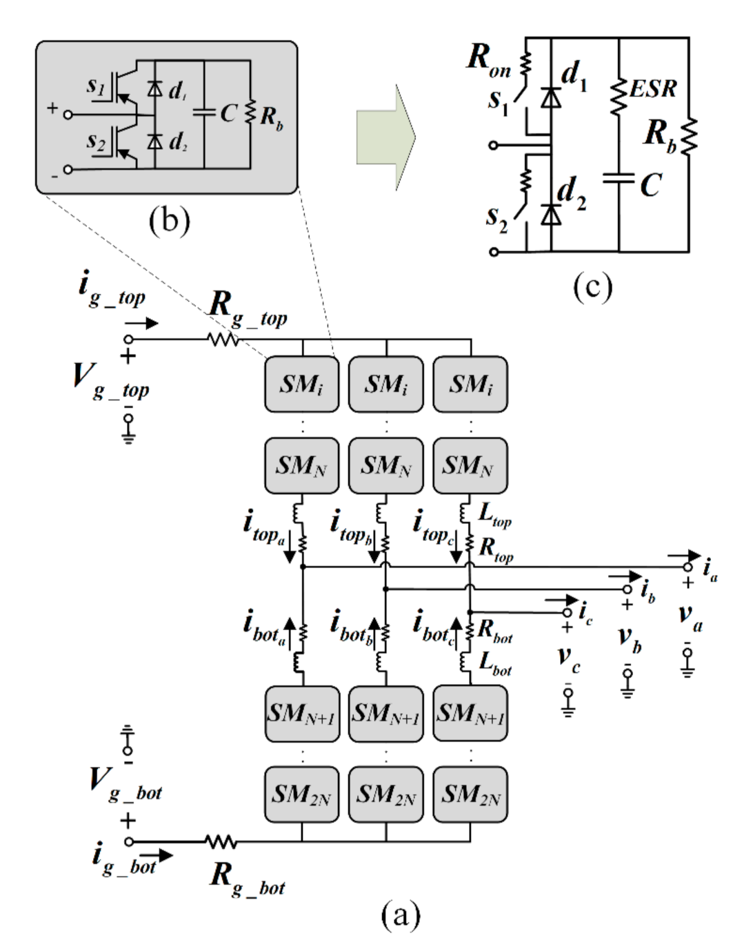
Let us consider as reference the circuit in
Figure 1a with bipolar DC Bus link voltages
and
, and three phase output voltages.
-subscript
is used to indicate phase a, b, and c. Each phase leg has a top and a bottom arm, each one having a number of SMs equal to
N. The arm equivalent resistance and inductance are
and
for the top arm and
and
for the bottom arm. As indicated in
Figure 1b, each SM is composed by two switching elements
and
with diodes (
,
) in parallel with a capacitor
and a bleed resistance
reflecting the MMC converter used to validate the simulation model.
and
are represented with a single pole single throw switch in series with its conduction resistance of value
. The capacitor is modelled with a capacitance of value
in series with its Equivalent Series Resistance (
). In the following model equations, each SM capacitor voltage is indicated as
where the subscript “
indicates the upper arm (SMs
) and the lower arm (SMs
).
The modes of operation considered are with the capacitor inserted or bypassed depending on the conduction state of the gates (, ) or the diodes (, ).
The state variables considered are the top and bottom arm inductance currents
,
and the capacitor voltages
. Equations (6) and (7) are obtained by writing a Kirchhoff Current Laws (KCL) for each SM respectively of the upper and lower arm. In these equations,
is the SM capacitance,
is the switching function. Depending on the gates values
and
-,
represents the conductance of the SM capacitor branch and
is the resistance value of the safety bleeding resistor of the real hardware MMC employed for model validation. The state-space Equations (8) and (9) are derived from the Kirchhoff Voltage Laws (KVL) written for each independent loop from the DC link to the AC load for each phase leading. The
can be equal to one or zero to respectively model the SM’s states inserted and bypassed. As indicated in the equations below,
depends on the gate states (
,
). Each gate can either be opened, in which case its state will be equal to 0, or closed, in which case it would be equal to 1. When the SM is inserted
then
and when it is bypassed
then
. During dead time state
the value of
is determined by the arm inductor current which according to its direction will flow into the proper diodes determining the SM’s state.
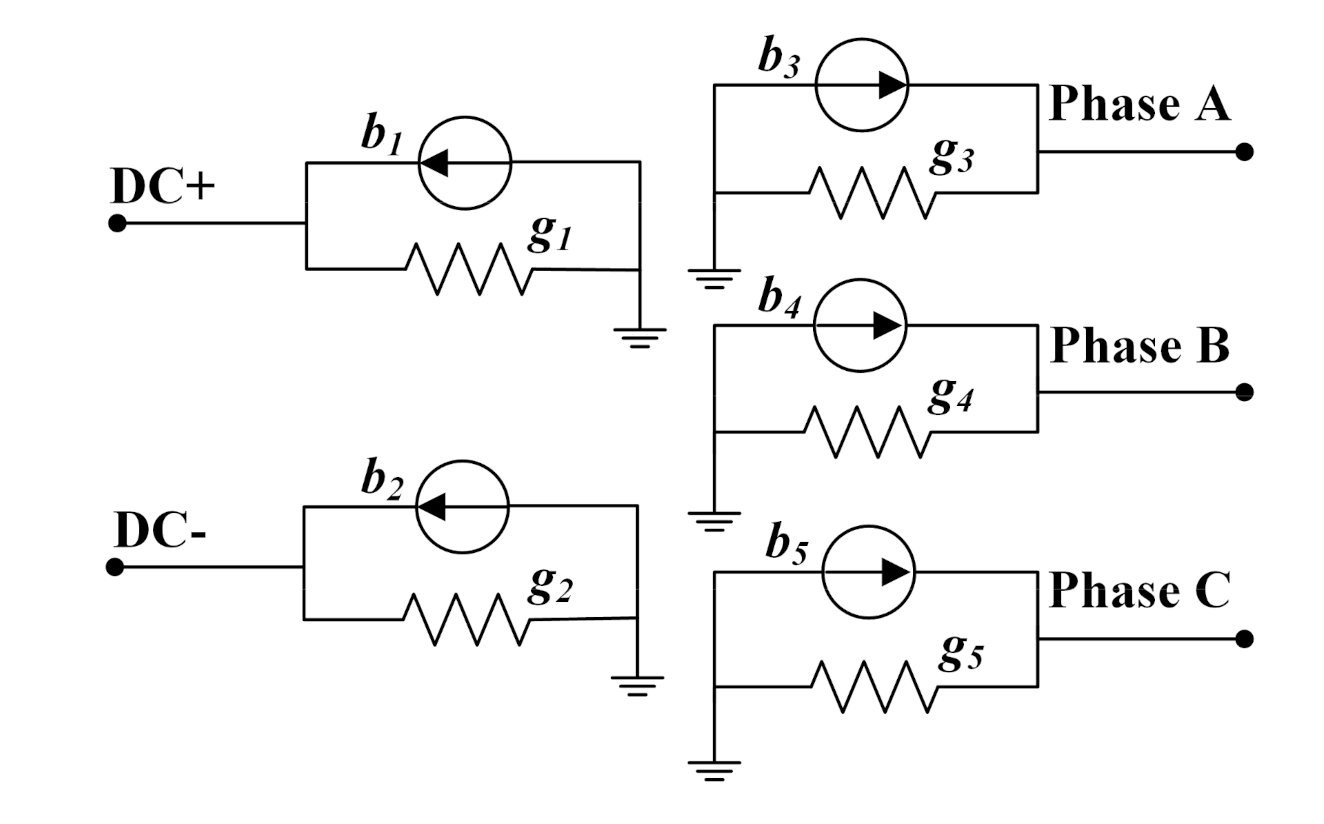
Applying the LB-LMC approach, the MMC model shown in
Figure 1 can be represented for the system level solution as an entity composed of five current-type ports, each one providing a current contribution
in parallel with a conductance
, with subscripts
corresponding to the component naming, as shown in
Figure 2. It is worth stressing that the developed MMC model is not an average model and the current sources of
Figure 2 are updated at each time step using the Equations (1)–(6) without any loss of information on the individual module switching behavior. The Equations (10)–(14) are used to compute the MMC equivalent LB-LMC model source contributions,
to
, based on the top
and bottom
arm currents computed by the state space Equations (6)–(9). The contributions,
and
are equal to the DC link currents while
to
are equal to the phase currents
.
At each simulation time step, the MMC current contributions are computed and used to compute the system solution as in (5). The nodal voltages of the DC link and of the three phase terminals
are then used at the next time step to update the state equations of the MMC converter. In Equation (5),
G is the system conductance matrix, precomputed and inverted offline (i.e., the inversion computations are not executed on the FPGA); x is the vector of the nodal voltages and
b is the vector of the currents contributions. The developed MMC model, together with other power electronics converter models, and the LB-LMC solver are distributed as an open-source package [
25,
26].
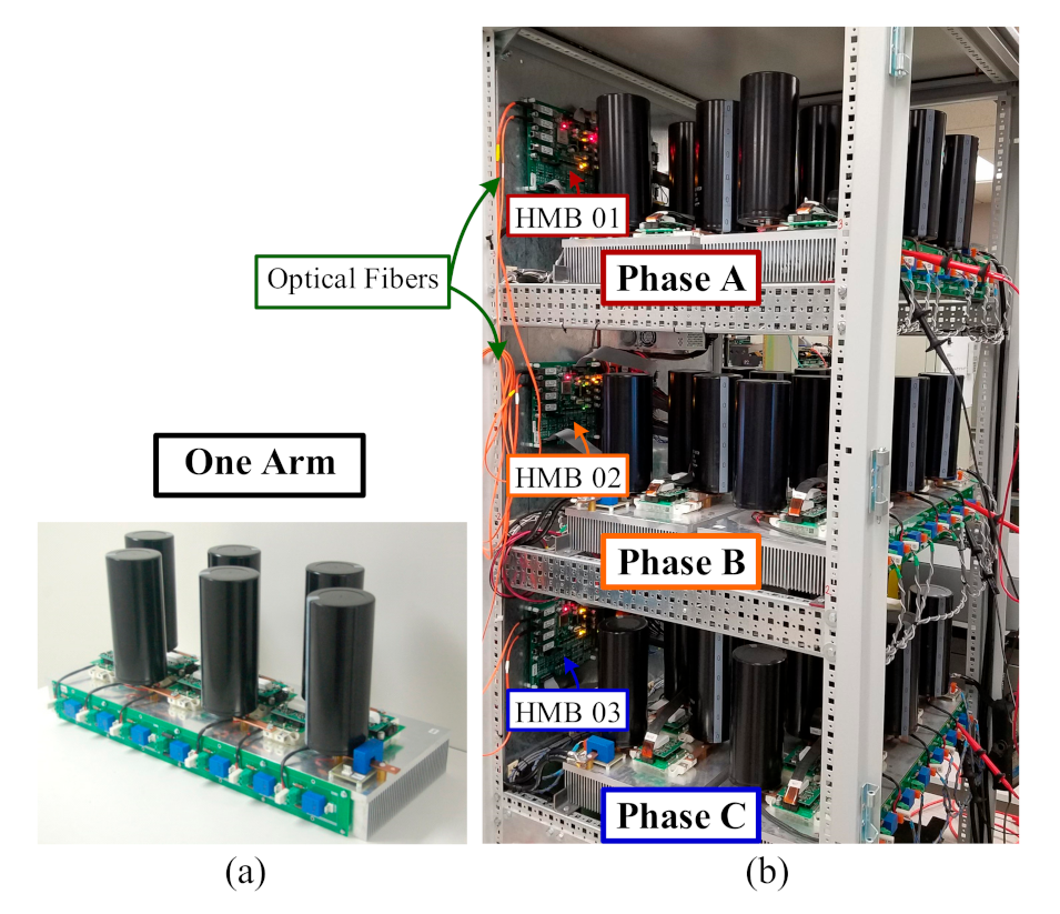
4. Hardware Reference System
An MMC prototype, shown in
Figure 3, is used for the model and HIL testing validation. The control hardware of the prototype is also used as Device Under Test (DUT) in the HIL testing. This MMC consists of six Half-Bridge (HB) SMs per arm. An SM is developed using the SEMIKRON SEMiX202GB066HDs HB IGBT module and the SEMIKRON SKYPER 32 PRO R IGBT gate driver triggers this IGBT module.
Table 1 lists the key parameters. The setup is designed for full load apparent power rating of 60k VA and the maximum DC bus voltage of 800 V. For flexibility purposes, the SM capacitance is 15 mF; the selection has been made based on market available capacitors’ size, cost, and ESR. Given the 15 mF of the SM capacitors and considering the peak magnitude of the double-fundamental-frequency circulating current,
I2f as 15 A the resulting value for arm inductors is 1 mH.
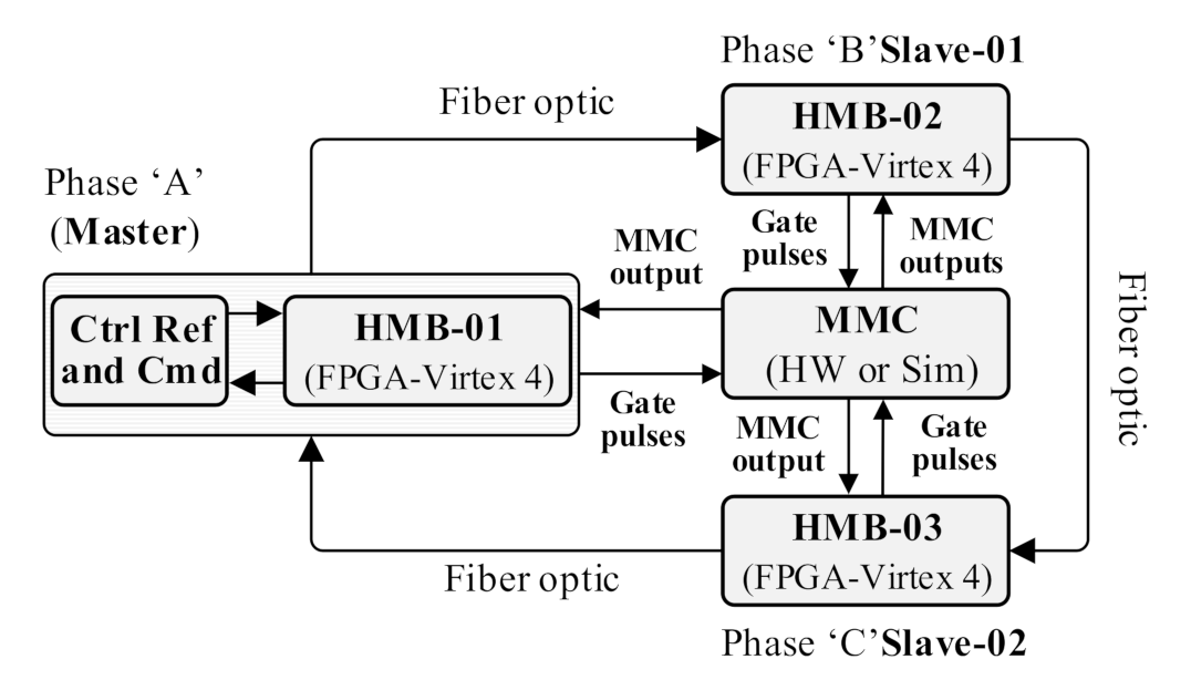
Each MMC phase is managed by a custom FPGA-based control platform, denoted as a Hardware Manager Board (HMB), which receives measurements from sensors and provides gate signals to each SM of its associated phase. Each HMB is composed of a Xilinx Virtex-4 XC4VFX20 FFG672 FPGA with four high-speed Multi-Gigabit Transceivers (MGT) and twenty analog-to-digital converters (ADC) channels. The ADCs are Texas Instruments (TI) ADS7863 which have four dual, 12-bit fully differential input channels grouped into two pairs for high-speed, simultaneous signal acquisition. Between HMBs, the three-phase ring communication is established using 8 bits of data width having 1.25 Gb/s line rate and a 125 MHz reference clock. The controller has a clock frequency CLK_C of 125 MHz.
For all three phases, the control modulating signal
m(t) is generated in the control master FPGA HMB-01 as depicted in
Figure 4.
HMB-01 also generates digital PWM gate signals and does the Voltage-Balancing (VB) for Phase A. HMB-02 and HMB-03 generates digital PWM gate signals and performs VB for Phase B and C, respectively. These two phase controllers (HMB-02 and HMB-03) receive
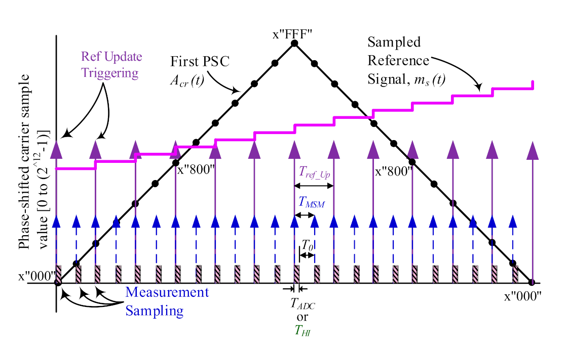
m(t) from HMB-01 via high speed optical fiber ring communication. The ring is a checksum-based custom communication protocol that is developed for data transfer between HMBs. In this work, the phase shifted carrier (PSC) pulse width modulation (PWM), detailed in [
27], is used. Since the MMC consists of six half-bridge SMs per arm, there are six 60° phase shifted carriers. The generation of the double updated modulating signal
ms(t) and measurement sampling trigger are illustrated in
Figure 5. Only the first triangular carrier is shown for clarity. The digital PWM gate signals are produced by comparing
ms(t) and the carrier signal
Acr(t). The switching frequency of the MMC,
fsw =
Nfc.
Since its double update control, thus the reference update period,
Tref_up is
Tsw/2. The measurement sampling has a period,
TMSM is equal to
Tref_up/2 or
Tsw/4. The operation of the HMBs is only different in the measurement section with respect to connection of the MMC hardware versus the simulator. For hardware experiments, when the measurement sampling event is up, it triggers the controller to receive new measurements from the MMC after
TADC time, that is the HMB ADC’s program and conversion time. For the CHIL experiment, when a measurement sampling event is up, the control updates the measurements coming from the simulation engine after
THI time, that is, the total time for one cycle of the CHIL. During
T0 time, the MMC measurements are stored in controller memory and the measurements are used for voltage balancing and protection of the system. The VB presented in [
28] has been used for this work.
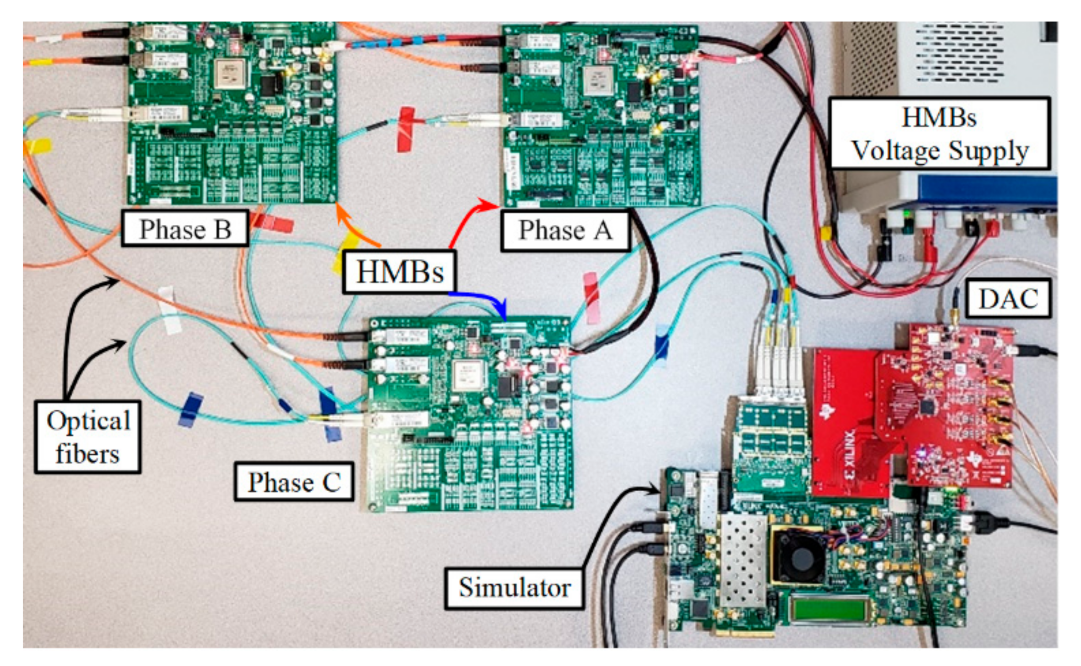
5. CHIL Setup
The HIL set-up is composed of three HMBs in addition to the FPGA-based MMC simulator with analog output capability for display of internal simulation variables. All connections between the control hardware and the MMC simulator are made via high-speed serial data channels. A picture of the CHIL set-up is shown in
Figure 6.
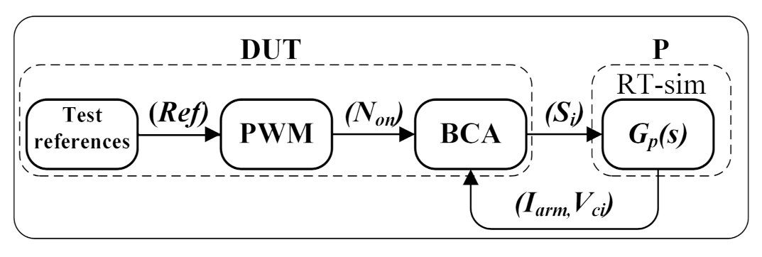
The block diagram of the complete structure of control system is reported in
Figure 7. The system main components are: the test references generator which outputs the three phases sinusoidal reference signals
{Ref}; the Phase-Shifted PWM (PWM) module which generates the modulation index values
; the voltage Balancing Control Algorithm (BCA); and the plant (MMC) represented by its transfer function
.
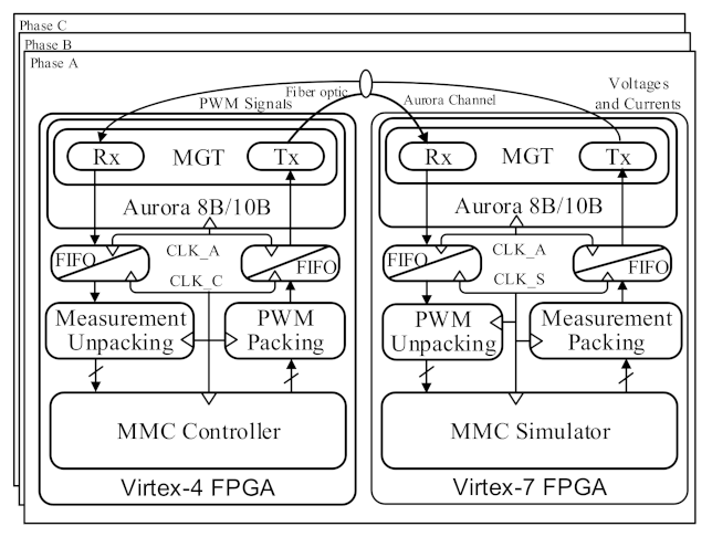
The section indicated by P is the section executed on the RT simulator; the rest of the control functions, including the BCA, are executed on the control platform. The data exchanged over the fiber optics are the SM switching pulses , the arm currents, and SM capacitors voltages .
5.1. RT Simulation FPGA Implementation
The MMC simulator is developed using a Virtex-7 FPGA. The core of the design is the simulation engine, MMC Simulator, discussed in [
15], which performs the RT simulation of the modeled system. This core computes solutions of the simulated model every time step using the LB-LMC method. Using a dataflow execution approach, the simulation engine computes all solutions in a single FPGA execution clock cycle set to the time step of the simulation for RT execution. To capture results from the simulation engine on the oscilloscope, a Digital-to-Analog Conversion (DAC) interface is used.
To allow the external controller platform access to the modeled system solved by the simulation engine, a control communication handler core exists in the top-level design.
5.2. Simulator Interface
A high-speed communication protocol using optical fibers interfaces the simulator to the DUT. A multi-gigabit communication between the MMC simulator and each HMB utilizes the Aurora protocol [
29] developed by Xilinx that uses 8B/10B data encoding. The Aurora 8B/10B protocol has several features such as channel bonding and clock compensation that simplify the establishment of high-speed Multi-Gigabit Transceivers (MGT)- based communication links [
30].
For this work, the Aurora 8B10B protocol consists of one lane, two bytes per lane, 1.50 Gb/s line rate, and 150 MHz reference clock.
Figure 8 illustrates the block diagram of Aurora 8B/10B interfacing each of MMC Simulator phases, namely Phase A, Phase B, and Phase C and the corresponding phase controller. For clock domain crossing (CDC) in-between controller or simulator and Aurora, first-in first-out (FIFO) has been used. Here, CLK_S, CLK_A, and CLK_C represents the clock for the simulator, Aurora protocol, and controller, respectively. The Aurora system clock CLK_A has a frequency of 75MHz while the simulator and controller have a frequency of 20 MHz and 125 MHz, respectively.
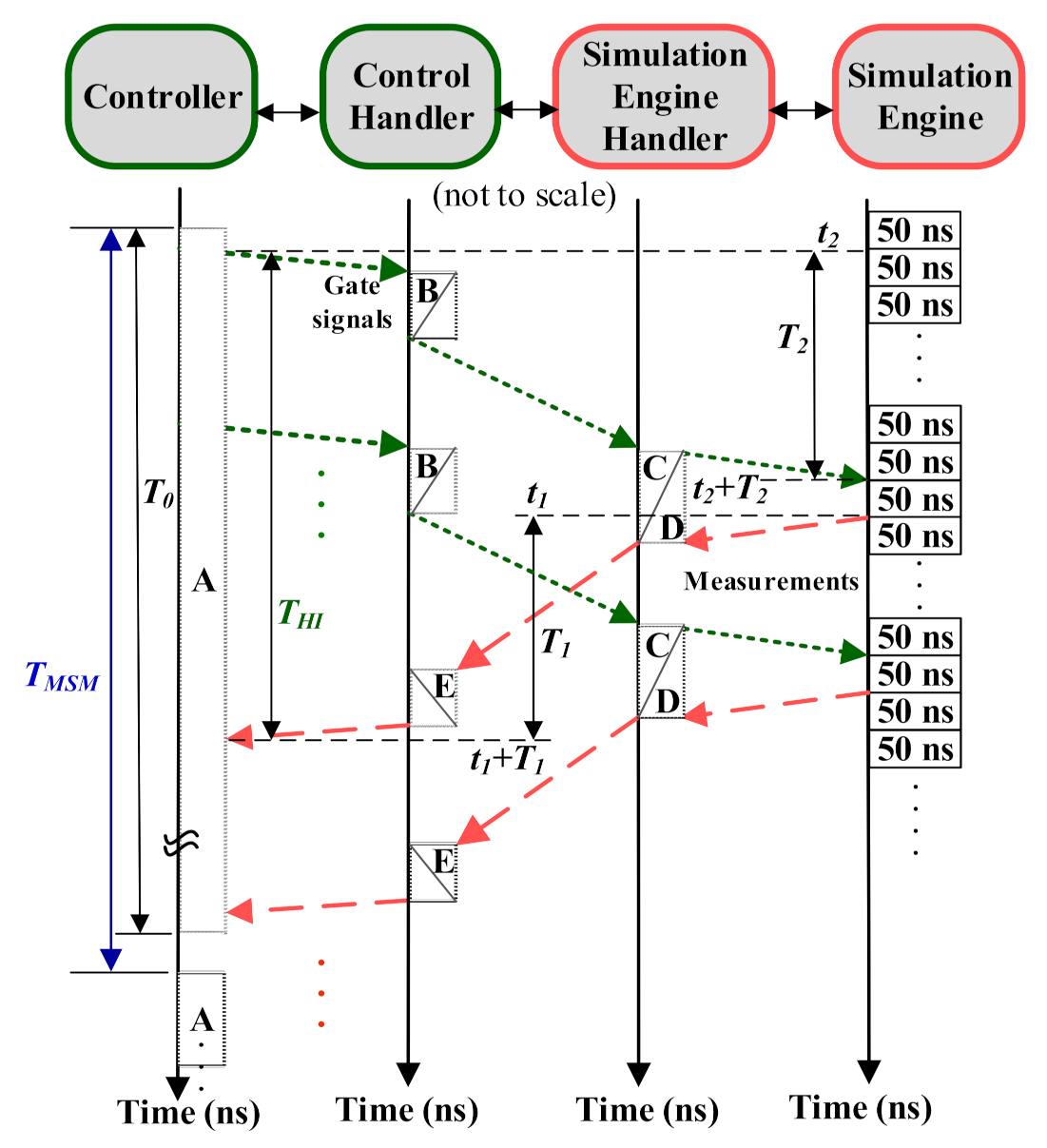
The timing of the interface between the control boards and the simulation engine is described in
Figure 9. At the top of the diagram, we indicate the main entities involved. They are the controller, which generates the gates signal; the control handler, the simulation engine handler, and finally the simulation engine. After initialization of Aurora communication, each controller HMB transmits gate signals to the simulation engine. The simulation engine receives the gate signals and sends out the measurements to the control as depicted in
Figure 8.
In
Figure 9, the white boxes indicated with letters represent the processes performed by each entity. Each process is described below:
Process A:
Performs the generation of PWM gate signals and then MMC capacitors voltages sorting and balancing. Process A has a time of . In this process, the HIL interfacing between phase controller and simulator happens continuously in a controlled manner.
Process B:
Takes care of packing the gates signals and of the clock domain crossing (CDC) between the controller clock CLK_C and the Aurora system clock CLK_A using FIFO as depicted in
Figure 8. Then the Aurora protocol transmits gate signal to the simulator FPGA platform.
Process C:
Takes care of unpacking the gates signals from Aurora channel and of the CDC between the Aurora system clock CLK_A and the Simulation Engine clock CLK_S. This process triggers as soon as it receives the desired header from the controller.
Process D:
Samples the MMC capacitor voltages and arm currents measurements from the simulation engine, and packs the samples. Furthermore, it also takes care of the CDC between CLK_S and CLK_A.
Process E:
Takes care of unpacking the MMC measurement samples from simulation engine and of the CDC between CLK_A and CLK_C using FIFO as illustrated in
Figure 8.
5.3. Communication Delay Estimation
Once the final PWM gate signals have been produced, they are sent out by process B. Ideally, the gate signals should have been received by the simulation engine at time but due to the delay introduced by the controller transmitting CDC and the Aurora-based communication system, those are received at time “”. has been estimated as approximately 1.7 µs. Similarly, is the time required for the MMC measurements from the simulator to be available in the controller. has been estimated to be approximately equal to 2.1 µs. The time is greater than since the amount of MMC measurement data to be sent out from the simulation engine is greater than the amount of data which has to be sent out by the control (the gates signals). It is clear that the introduced delay will affect the HIL experiment accuracy. In the next section, we will evaluate the impact of these delays.
6. Experimental Result
6.1. MMC Model Validation
The validation of simulation model is of particular importance in the evaluation of a simulation method. In this paper this is even more critical when we analyze the performance of the proposed Aurora interface. Some reference work for validation of MMC models are reported here: [
31,
32,
33]. In order to clarify the effectiveness of the presented work, a model validation has been conducted comparing the MMC phase and capacitor voltages and circulating currents waveforms with the ones obtained by operating a real MMC. The accuracy has been evaluated by computing the two-norm error. The laboratory prototype MMC described in
Section 4 has been used to validate the MMC model and is referred here as HW. The model is executed on a CPU-based workstation and it is referred to here as Csim.
For validation purposes, Csim and the real MMC implement the same control logic, a DC bus voltage of 620 V and a resistive load power of 4.5 kW. The results have been compared by computing a two-norm error. The general formula for a p-order norm error
is presented in (15). Here
indicates the norm class is set equal to two since the Euclidean norm for the error calculation is considered. The series of
reference samples indicated by subscript
, used to compute the error is
while the series of measured samples for which the error is evaluated with respect to the reference is indicated as
.
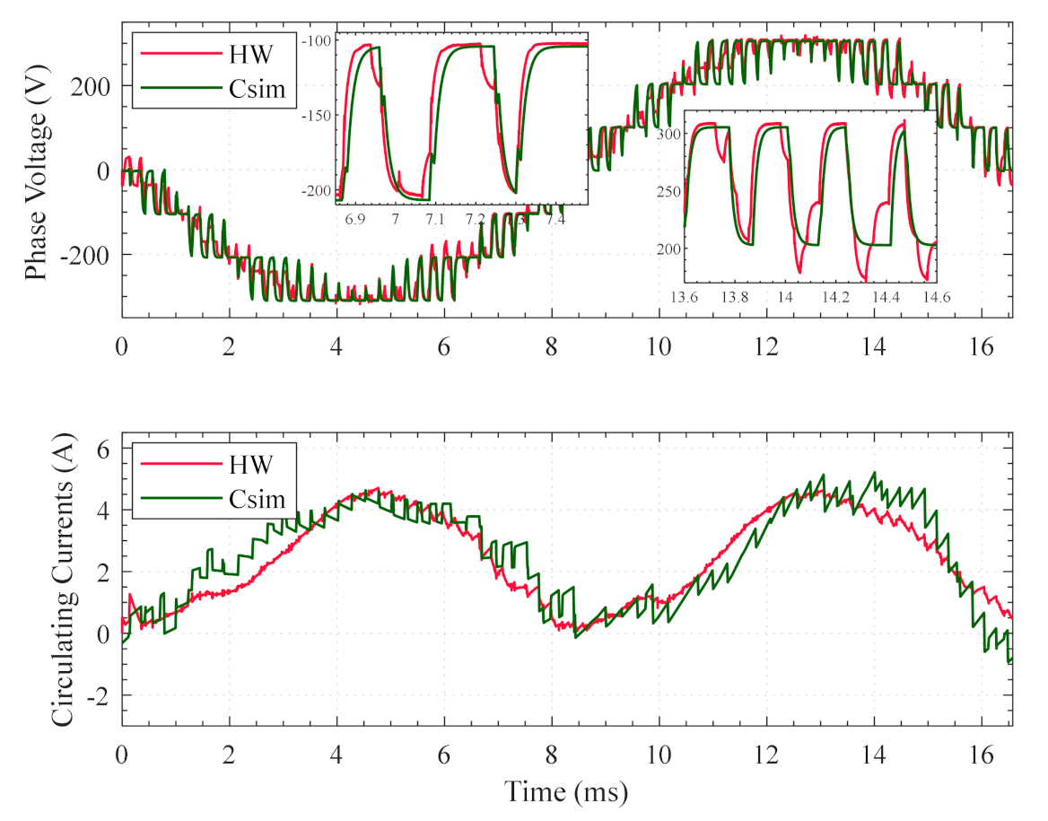
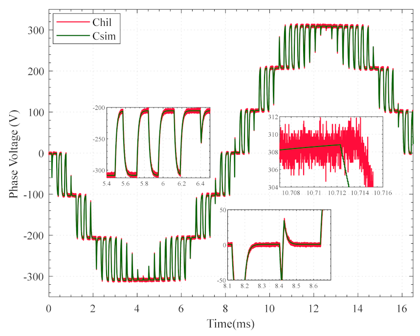
The two-norm error of the phase voltage depicted in
Figure 10a is equal to 8.7%. In this case, the results from the HW execution correspond to
while the results from the Csim simulation correspond to
. Differences in the phase voltages shown in
Figure 10a are mainly due to circulating current differences between the hardware experiment and simulation as shown in
Figure 10b. This is mainly due to the mismatch of passive elements between the module capacitor and bleeding resistance.
The results reported in this paper are obtained by randomizing the values of these passive elements considering the fabrication tolerance around their nominal value. In this way, we obtained a good match without matching each individual parameter and so kept the model of more general interest.
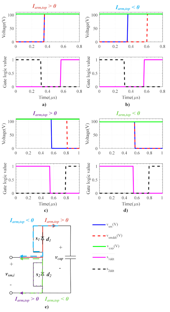
In order to demonstrate the free willing diode behavior—somehow unusual in switching function-based models—we analyze the dead time behavior of an individual module.
With reference to
Figure 11, the quantities considered for the analysis are the voltage at the SM’s terminals for a model without dead time
and for the model with diodes and dead times
. The voltages should approach the capacitor voltage
when the SM is inserted and zero when the SM bypassed. The leg A top arm current
is considered. When positive, it will flow through diode
else diode
.
In
Figure 11, we report the four typical conditions for analyzing the dead time behavior of a half bridge topology; in
Figure 11a with the SM transitioning to inserted mode and positive current and
Figure 11d with the SM transitioning to bypassed mode and negative current, the dead time effect is not visible since the diode conducting is in parallel to the switch conducting after the transition. Vice versa, the effect is easily visible in
Figure 11b,c where the diode conducting during the dead time is in parallel with the switch conducting before the transition. Those conditions reflected on the SM circuit with corresponding arm current color are illustrated in
Figure 11e.
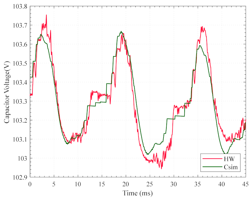
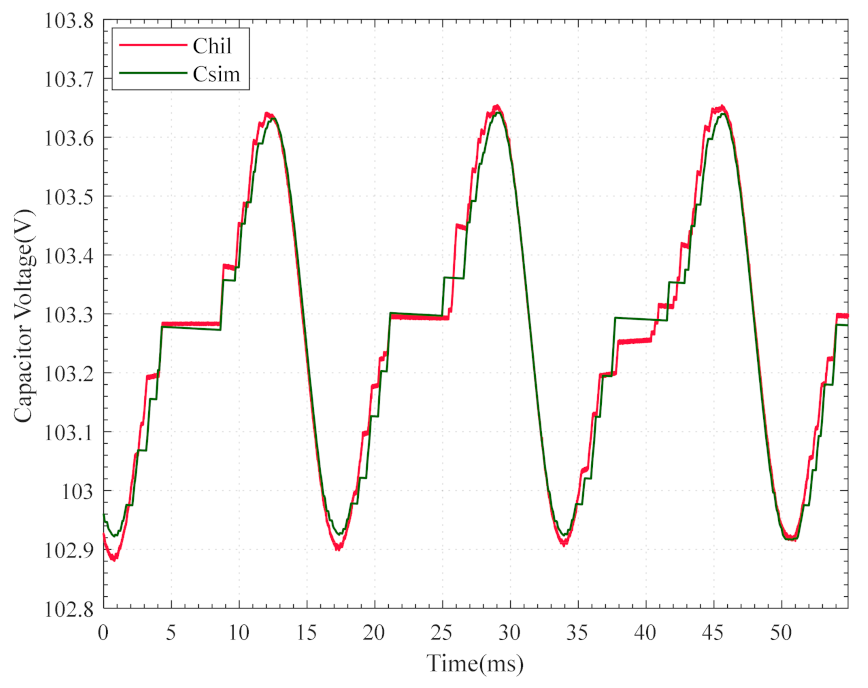
To conclude the model validation in
Figure 12, we compare the phase A 1st capacitor voltage computed by the simulation model with the one acquired from the MMC prototype. For 620 V DC bus voltage, the average value of capacitor voltage is as expected 103.33 V.
In this case, rather than directly computing the two-norm error, which would have been meaninglessly small due to the large offset of the signals, we calculate the percentage error
by first removing the DC component. The formula for calculating
is reported in (16).
As in (15), the error in this case is also computed considering two series of samples, where each sample is indicated by a subscript . A sample of the measured values for which the error is evaluated is indicated as while a sample of the reference values is indicated as . Finally is the normalization reference value used in the denominator of the error formula in order to compute the percentage for which the factor is introduced. For the case of the MMC model validation presented here, is a sample of the Csim capacitor voltage minus its average computed over the entire timespan of the simulation, while , is a sample of the HW MMC capacitor voltage minus its average value computed over the same time span of the Csim. The denominator is the maximum peak–peak amplitude of the HW capacitor voltage. The error allows better appreciation of the differences in amplitude, which are at least three orders of magnitude below the waveform mean value. The value of for the MMC model validation is 7.3%.
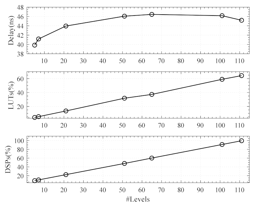
6.2. Scalability Analysis
Since the goal of this work is to support power electronic system level analysis while maintaining a detailed temporal resolution, it is important that we test the scalability of the proposed model. For this purpose, we considered the Xilinx Virtex-7 485t VC707 FPGA and a fixed simulation time step of 50 ns.
First, we considered the scalability of the simulator when the number of modules in a single MMC is increased. In
Figure 13, we report the results of the scalability analysis for a single converter when the number of levels is increased from 7 to 111.
As expected, and as highlighted by previous work on the LB-LMC method, the computational delay remains relatively constant. The variations are due to the effort of Vivado tool to best place and route the design, and the resource usage scales linearly.
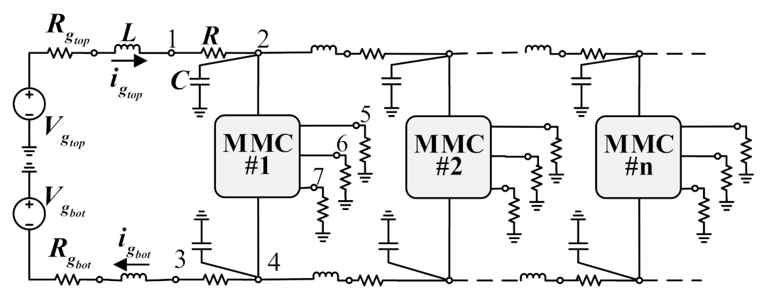
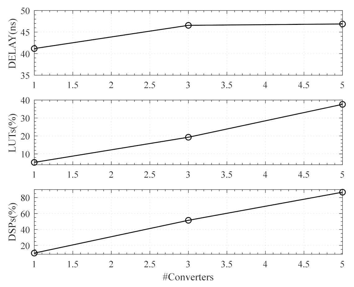
We also analyzed the scalability of the proposed approach when multiple converters are modelled. For this purpose, we used the microgrid of
Figure 14, where converters are added one after the other to increase the system size.
Since we used a single cycle data flow approach to execution and due to the intuitive consideration that similar model components require the same amount of resources, we expected to observe again a linear scaling of the resource usage.
Figure 15 shows the stability results when an increasing number of 7-level MMC converters are added to the system. As expected, the results show a linear relation between the system size and the resources usage.
The maximum number of switching devices included in the simulation for the two scalability analyses is much greater in the converter-size scalability analysis (660 sub-modules) than in the case of the grid-size one (180 sub-modules). This is because in the latter case, systems with more converters have larger conductance matrixes (each converter introduces 7 more nodes) which require larger FPGA resources allocation. Further scalability can be ensured using a multi-FPGA solution as described in [
34].
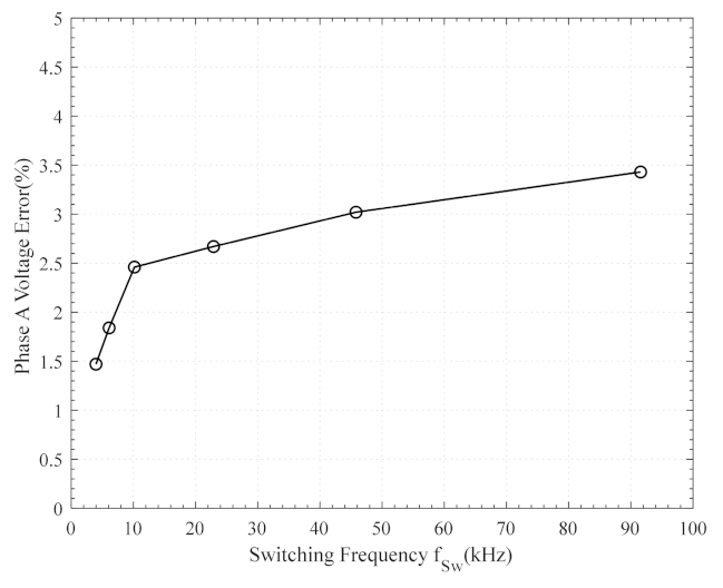
6.3. Communication-Based CHIL Accuracy
In this section, to determine the accuracy of the CHIL, the results obtained by the CHIL tests are compared with the Csim results validated in the previous section. As we will show, the impact of the communication delay is quite small. To better appreciate the impact of the delay, we decided to compare the results obtained by the CHIL experiment with the one of the Csim. Later in the paper, we will also compare the CHIL results with the data collected using the hardware prototype.
In
Figure 16, the phase A voltage waveform output from Csim and from the CHIL experiment are superimposed. The main difference between the
and the CHIL results is that in the latter, the use of a communication protocol (Aurora) as CHIL interface, induce the communication delays
and
,
Figure 9. They cause the CHIL waveform to be delayed with respect to the Csim waveform by 2 μs, as can be observed by the detailed zoom of
Figure 16.
Overall, the inaccuracy introduced by the communication delay is small and the two-norm error in this case is equal to 1.47%.
Similarly in
Figure 17 we report the phase A 1st capacitor voltage waveforms; in this case the error as computed according to (16) is equal to 2.87%.
The presence of the communication delays represents a limitation for the CHIL platform, especially with regard to the delay between when the controller updates the state of the gate signals and when the update values are received by the simulator,
. The negative effect of this delay will be more significant for converters switching at higher switching frequencies. To quantify the impact of communication delay on CHIL error, a new C-simulation, namely CsimT1T2, emulating the effects of the communication delays
and
, has been developed and executed for MMC with increasing switching frequency. For each case the two-norm error considering the Csim as reference has been computed and the results are shown in
Figure 18.
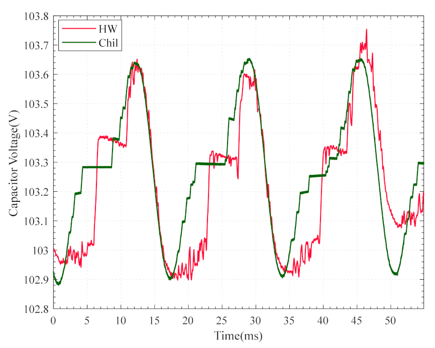
6.4. Comparison of CHIL and Real Hardware Results
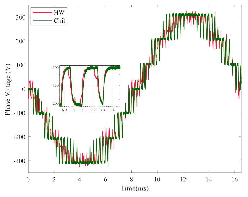
In this section, the accuracy of the CHIL simulator is evaluated by comparing it against the real MMC. In
Figure 19, the phase A voltage waveforms of both cases are superimposed, the same is done in
Figure 20 for the 1st capacitor voltage of phase A.
The two-norm error of the phase voltage in this case is equal to 8.6% while the of the cap voltages is equal to 12%. Those values are very much comparable to the one obtained in the model validation phase, so we can then say that for this application the error introduced using a protocol-based CHIL interface is very limited and that the accuracy of the CHIL experiment is mainly determined by the accuracy of the model and not by the CHIL interface.


 ,
, 


