Thermal Characterization and Modelling of AlGaN-GaN Multilayer Structures for HEMT Applications †


Abstract
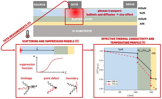
1. Introduction
2. Materials and Methods
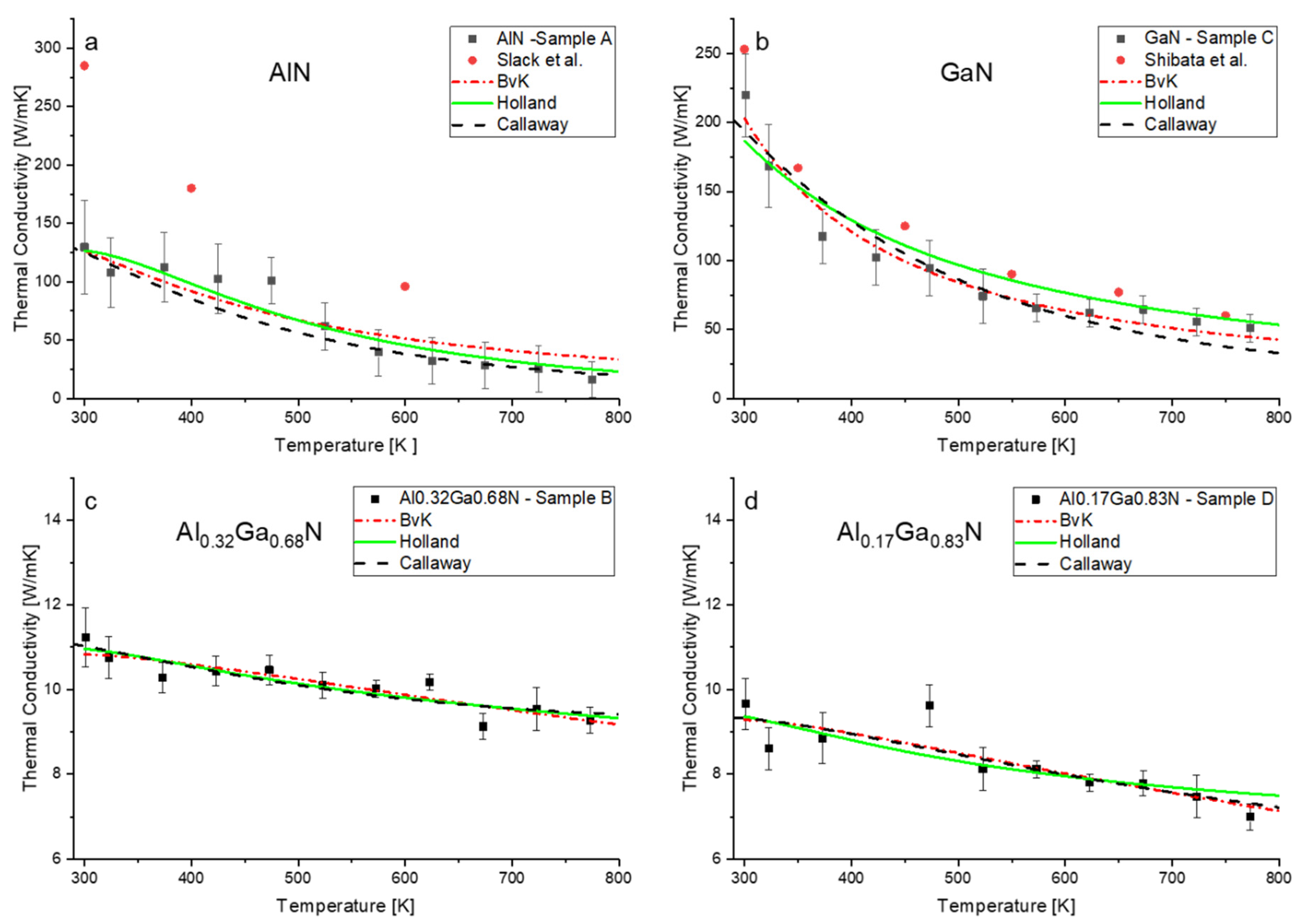
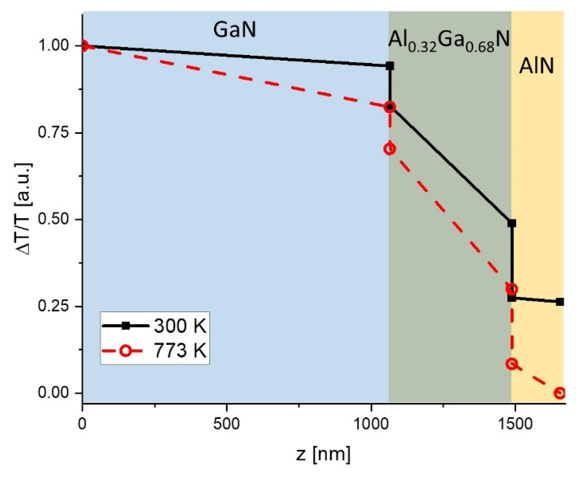
3. Results
4. Modelling Methodology and Discussion
4.1. Thermal Interface Conductance
4.2. Models for Phonon Scattering
4.3. Models for the Size Effect in Cross-Plane Thermal Transport
5. Conclusions
Author Contributions
Funding
Acknowledgments
Conflicts of Interest
Appendix A
References
- Baskaran, S.; Mohanbabu, A.; Anbuselvan, N.; Mohankumar, N.; Godwinraj, D.; Sarkar, C.K. Modeling of 2DEG sheet carrier density and DC characteristics in spacer based AlGaN/AlN/GaN HEMT devices. Superlattices Microstruct. 2013, 64, 470–482. [Google Scholar] [CrossRef]
- Mishra, U.K.; Shen, L.; Kazior, T.E.; Wu, Y.-F. GaN-based RF power devices and amplifiers. Proc. IEEE 2008, 96, 287–305. [Google Scholar] [CrossRef]
- Fitch, R.C.; Walker, D.E.; Green, A.J.; Tetlak, S.E.; Gillespie, J.K.; Gilbert, R.D.; Sutherlin, K.A.; Gouty, W.D.; Theimer, J.P.; Via, G.D.; et al. Implementation of high-power-density X-band AlGaN/GaN high electron mobility transistors in a millimeter-wave monolithic microwave integrated circuit process. IEEE Electron Device Lett. 2015, 36, 1004–1007. [Google Scholar] [CrossRef]
- Luo, X.; Halder, S.; Curtice, W.R.; Hwang, J.C.M.; Chabak, K.D.; Dennis, E.; Dabiran, A.M. Scaling and high-frequency performance of AlN/GaN HEMTs. In Proceedings of the IEEE International Symposium on Radio-Frequency Integration Technology, Beijing, China, 30 November–2 December 2011. [Google Scholar] [CrossRef]
- Vallabhaneni, A.K.; Chen, L.; Gupta, M.P.; Kumar, S. Solving nongray boltzmann transport equation in gallium nitride. J. Heat Transf. 2017, 139. [Google Scholar] [CrossRef]
- Yalamarthy, A.S.; So, H.; Muñoz Rojo, M.; Suria, A.J.; Xu, X.; Pop, E.; Senesky, D.G. Tuning electrical and thermal transport in AlGaN/GaN heterostructures via buffer layer engineering. Adv. Funct. Mater. 2018, 28. [Google Scholar] [CrossRef]
- Hao, Q.; Zhao, H.; Xiao, Y.; Kronenfeld, M.B. Electrothermal studies of GaN-based high electron mobility transistors with improved thermal designs. Int. J. Heat Mass Transf. 2018, 116, 496–506. [Google Scholar] [CrossRef]
- Zhang, G.-C.; Feng, S.-W.; Zhou, Z.; Li, J.-W.; Guo, C.-S. Evaluation of thermal resistance constitution for packaged AlGaN/GaN high electron mobility transistors by structure function method. Chin. Phys. B 2011, 20, 027202. [Google Scholar] [CrossRef]
- Sarua, A.; Ji, H.; Hilton, K.P.; Wallis, D.J.; Uren, M.J.; Martin, T.; Kuball, M. Thermal boundary resistance between GaN and substrate in AlGaN/GaN electronic devices. IEEE Trans. Electron Devices 2007, 54, 3152–3158. [Google Scholar] [CrossRef]
- Cho, J.; Bozorg-Grayeli, E.; Altman, D.H.; Asheghi, M.; Goodson, K.E. Low thermal resistances at GaN-SiC interfaces for HEMT technology. IEEE Electron Device Lett. 2012, 33, 378–380. [Google Scholar] [CrossRef]
- Freedman, J.P.; Leach, J.H.; Preble, E.A.; Sitar, Z.; Davis, R.F.; Malen, J.A. Universal phonon mean free path spectra in crystalline semiconductors at high temperature. Sci. Rep. 2013, 3. [Google Scholar] [CrossRef]
- Cheng, Z.; Koh, Y.R.; Mamun, A.; Shi, J.; Bai, T.; Huynh, K.; Yates, L.; Liu, Z.; Li, R.; Lee, E.; et al. Experimental Observation of High Intrinsic Thermal Conductivity of AlN. Available online: https://arxiv.org/ftp/arxiv/papers/1911/1911.01595.pdf (accessed on 10 April 2020).
- Park, K.; Bayram, C. Impact of dislocations on the thermal conductivity of gallium nitride studied by time-domain thermoreflectance. J. Appl. Phys. 2019, 126. [Google Scholar] [CrossRef]
- Liu, W.; Balandin, A.A. Thermal conduction in AlxGa1-xN alloys and thin films. J. Appl. Phys. 2005, 97, 1–6. [Google Scholar] [CrossRef]
- Chatterjee, B.; Dundar, C.; Beechem, T.E.; Heller, E.; Kendig, D.; Kim, H.; Donmezer, N.; Choi, S. Nanoscale electro-thermal interactions in AlGaN/GaN high electron mobility transistors. J. Appl. Phys. 2020, 127. [Google Scholar] [CrossRef]
- Lundh, J.S.; Chatterjee, B.; Song, Y.; Baca, A.G.; Kaplar, R.J.; Beechem, T.E.; Allerman, A.A.; Armstrong, A.M.; Klein, B.A.; Bansal, A.; et al. Multidimensional thermal analysis of an ultrawide bandgap AlGaN channel high electron mobility transistor. Appl. Phys. Lett. 2019, 115. [Google Scholar] [CrossRef]
- Yang, F.; Dames, C. Mean free path spectra as a tool to understand thermal conductivity in bulk and nanostructures. Phys. Rev. B Condens. Matter Mater. Phys. 2013, 87, 1–12. [Google Scholar] [CrossRef]
- Regner, K.T.; Wei, L.C.; Malen, J.A. Interpretation of thermoreflectance measurements with a two-temperature model including non-surface heat deposition. J. Appl. Phys. 2015, 118. [Google Scholar] [CrossRef]
- Hua, C.; Minnich, A.J. Semi-analytical solution to the frequency-dependent Boltzmann transport equation for cross-plane heat conduction in thin films. J. Appl. Phys. 2015, 117. [Google Scholar] [CrossRef]
- Regner, K.T.; Freedman, J.P.; Malen, J.A. Advances in studying phonon mean free path dependent contributions to thermal conductivity. Nanoscale Microscale Thermophys. Eng. 2015, 19, 183–205. [Google Scholar] [CrossRef]
- Guo, Y.; Wang, M. Phonon hydrodynamics for nanoscale heat transport at ordinary temperatures. Phys. Rev. B 2018, 97, 1–27. [Google Scholar] [CrossRef]
- Reisinger, M.; Tomberger, M.; Zechner, J.; Daumiller, I.; Sartory, B.; Ecker, W.; Keckes, J.; Lechner, R.T.T. Resolving alternating stress gradients and dislocation densities across AlxGa1-xN multilayer structures on Si(111). Appl. Phys. Lett. 2017, 111. [Google Scholar] [CrossRef]
- Netzsch (Ed.) Thermoreflectance by Pulsed Light Heating Thermoreflectance–NanoTR/PicoTR. Available online: https://www.netzsch-thermal-analysis.com/de/produkte-loesungen/waerme-und-temperatur-leitfaehigkeitsbestimmung/nanotrpicotr/ (accessed on 4 May 2020).
- Fladischer, K.; Leitgeb, V.; Mitterhuber, L.; Keckes, J.; Sagmeister, M.; Carniello, S. Combined thermo-physical investigations of thin layers with Time Domain Thermoreflectance and Scanning Thermal Microscopy on the example of 500 nm thin, CVD grown tungsten. Thermochim. Acta 2019. [Google Scholar] [CrossRef]
- Cahill, D.G. Analysis of heat flow in layered structures for time-domain thermoreflectance. Rev. Sci. Instrum. 2004, 75, 5119–5122. [Google Scholar] [CrossRef]
- Yang, J.; Ziade, E.; Schmidt, A.J. Uncertainty analysis of thermoreflectance measurements. Rev. Sci. Instrum. 2016, 87, 1–11. [Google Scholar] [CrossRef] [PubMed]
- Glassbrenner, C.J.; Slack, G.A. Thermal conductivity of silicon and germanium from 3°K to the melting point. Phys. Rev. 1964, 134, A1058. [Google Scholar] [CrossRef]
- Corruccini, R.J.; Gniewek, J.J. Specific Heats and Enthalpies of Technical Solids at Low Temperatures; National Bureau of Standards: Washington, DC, USA, 1960. [CrossRef]
- Palankovski, V.; Quay, R. Analysis and Simulation of Heterostructure Devices; Springer: Wien, Austria, 2004. [Google Scholar] [CrossRef]
- Danilchenko, B.A.; Paszkiewicz, T.; Wolski, S.; Jezowski, A.; Plackowski, T. Heat capacity and phonon mean free path of wurtzite GaN. Appl. Phys. Lett. 2006, 89. [Google Scholar] [CrossRef]
- Mitterhuber, L.; Hammer, R.; Dengg, T.; Fladischer, K.; Spitaler, J. Thermal investigation of AlGaN-GaN multilayer structures. In Proceedings of the THERMINIC 2019-25th International Workshop on Thermal Investigations of ICs and Systems, Lecco, Italy, 25–27 September 2019. [Google Scholar] [CrossRef]
- Slack, G.A.; Tanzilli, R.A.; Pohl, R.O.; Vandersande, J.W. The intrinsic thermal conductivity of AIN. J. Phys. Chem. Solids 1987, 48, 641–647. [Google Scholar] [CrossRef]
- Abeles, B. Lattice thermal conductivity of disordered semiconductor alloys at high temperatures. Phys. Rev. 1963, 131, 1906–1911. [Google Scholar] [CrossRef]
- Daly, B.C.; Maris, H.J.; Nurmikko, A.V.; Kuball, M.; Han, J. Optical pump-and-probe measurement of the thermal conductivity of nitride thin films. J. Appl. Phys. 2002, 92, 3820–3824. [Google Scholar] [CrossRef]
- Shibata, H.; Waseda, Y.; Ohta, H.; Kiyomi, K.; Shimoyama, K.; Fujito, K.; Nagaoka, H.; Kagamitani, Y.; Simura, R.; Fukuda, T. High thermal conductivity of gallium nitride (GaN) crystals grown by HVPE Process. Mater. Trans. 2007, 48, 2782–2786. [Google Scholar] [CrossRef]
- Berg, W.T. The low temperature heat capacity of platinum. J. Phys. Chem. Solids 1969, 30, 69–72. [Google Scholar] [CrossRef]
- Hopkins, P.E.; Norris, P.M.; Stevens, R.J. Influence of inelastic scattering at metal-dielectric interfaces. J. Heat Transf. 2008, 130, 022401. [Google Scholar] [CrossRef]
- Stanley, C.M.; Estreicher, S.K. Phonon dynamics at an oxide layer in silicon: Heat flow and Kapitza resistance. Phys. Status Solidi Appl. Mater. Sci. 2019, 216, 1–9. [Google Scholar] [CrossRef]
- Hopkins, P.E.; Norris, P.M. Relative Contributions of inelastic and elastic diffuse phonon scattering to thermal boundary conductance across solid interfaces. J. Heat Transf. 2009, 131, 22402. [Google Scholar] [CrossRef]
- Hopkins, P.E.; Duda, J.C.; Clark, S.P.; Hains, C.P.; Rotter, T.J.; Phinney, L.M.; Balakrishnan, G. Effect of dislocation density on thermal boundary conductance across GaSb/GaAs interfaces. Appl. Phys. Lett. 2011, 98. [Google Scholar] [CrossRef]
- Swartz, E.T.; Pohl, R.O. Thermal boundary resistance. Rev. Mod. Phys. 1989, 61, 605–668. [Google Scholar] [CrossRef]
- Stoner, R.J.; Maris, H.J. Kapitza conductance and heat-Flow between solids at temperatures from 50 to 300K. Phys. Rev. B 1993, 48, 16373–16387. [Google Scholar] [CrossRef]
- Norris, P.M.; Hopkins, P.E. Examining interfacial diffuse phonon scattering through transient thermoreflectance measurements of thermal boundary conductance. J. Heat Transf. 2009, 131, 043207. [Google Scholar] [CrossRef]
- Keune, W.; Hong, S.; Hu, M.Y.; Zhao, J.; Toellner, T.S.; Alp, E.E.; Sturhahn, W.; Rahman, T.S.; Roldan Cuenya, B. Influence of interfaces on the phonon density of states of nanoscale metallic multilayers: Phonon confinement and localization. Phys. Rev. B 2018, 98, 1–16. [Google Scholar] [CrossRef]
- Callaway, J. Model for lattice thermal conductivity at low temperatures. Phys. Rev. 1959, 113, 1046–1051. [Google Scholar] [CrossRef]
- Morelli, D.T.; Heremans, J.P.; Slack, G.A. Estimation of the isotope effect on the lattice thermal conductivity of group IV and group III-V semiconductors. Phys. Rev. B Condens. Matter Mater. Phys. 2002, 66, 1953041–1953049. [Google Scholar] [CrossRef]
- Jugdersuren, B.; Kearney, B.T.; Queen, D.R.; Metcalf, T.H.; Culbertson, J.C.; Chervin, C.N.; Stroud, R.M.; Nemeth, W.; Wang, Q.; Liu, X. Thermal conductivity of amorphous and nanocrystalline silicon films prepared by hot-wire chemical-vapor deposition. Phys. Rev. B 2017, 96, 1–8. [Google Scholar] [CrossRef]
- Chen, G. Size and interface effects on thermal conductivity of superlattices and periodic thin-film structures. J. Heat Transf. 1997, 119, 220–229. [Google Scholar] [CrossRef]
- Peierls, R. Zur kinetischen Theorie der Wärmeleitung in Kristallen. Ann. Phys. 1929, 395, 1055–1101. [Google Scholar] [CrossRef]
- Klemens, P.G.; White, G.K.; Tainsh, R.J. Scattering of lattice waves by point defects. Philos. Mag. 1962, 7, 1323–1335. [Google Scholar] [CrossRef]
- Wang, Z.; Alaniz, J.E.; Jang, W.; Garay, J.E.; Dames, C. Thermal conductivity of nanocrystalline silicon: Importance of grain size and frequency-dependent mean free paths. Nano Lett. 2011, 11, 2206–2213. [Google Scholar] [CrossRef]
- Toberer, E.S.; Zevalkink, A.; Snyder, G.J. Phonon engineering through crystal chemistry. J. Mater. Chem. 2011, 21, 15843–15852. [Google Scholar] [CrossRef]
- Alekseeva, G.T.; Efimova, B.A.; Ostrovskaya, L.M.; Serebryannikova, O.S.; Tsypin, M.I. Thermal conductivity of solid solutions based on lead telluride. Sov. Phys. Semicond. 1971, 4, 1122–1125. [Google Scholar]
- Dengg, T.; Razumovskiy, V.; Romaner, L.; Kresse, G.; Puschnig, P.; Spitaler, J. Thermal expansion coefficient of WRe alloys from first principles. Phys. Rev. B 2017, 96. [Google Scholar] [CrossRef]
- Kresse, G.; Furthmüller, J. Efficient iterative schemes for ab initio total-energy calculations using a plane-wave basis set. Phys. Rev. B Condens. Matter Mater. Phys. 1996, 54, 11169–11186. [Google Scholar] [CrossRef]
- Fan, Z.; Dong, H.; Harju, A.; Ala-Nissila, T. Homogeneous nonequilibrium molecular dynamics method for heat transport and spectral decomposition with many-body potentials. Phys. Rev. B 2019, 99, 1–9. [Google Scholar] [CrossRef]
- Sondheimer, E.H. The mean free path of electrons in metals. Adv. Phys. 1952, 1, 1–42. [Google Scholar] [CrossRef]
- Beechem, T.E.; McDonald, A.E.; Fuller, E.J.; Talin, A.A.; Rost, C.M.; Maria, J.P.; Gaskins, J.T.; Hopkins, P.E.; Allerman, A.A. Size dictated thermal conductivity of GaN. J. Appl. Phys. 2016, 120. [Google Scholar] [CrossRef]
- Hodges, C.; Anaya Calvo, J.; Stoffels, S.; Marcon, D.; Kuball, M. AlGaN/GaN field effect transistors for power electronics - Effect of finite GaN layer thickness on thermal characteristics. Appl. Phys. Lett. 2013, 103. [Google Scholar] [CrossRef]


| Materials | [m/s] | n [Å−3] | M [kg] | [kg/m³] | |||
|---|---|---|---|---|---|---|---|
| AlN | 1.77 | 10,751 | 6027 | 6406 | 0.0941 | 3.48 × 10⁻²⁶ | 3201 |
| GaN | 2.05 | 7538 | 4022 | 4566 | 0.0852 | 6.95 × 10⁻²⁶ | 5923 |
| Al0.32Ga0.68N | 1.91 | 8962 | 4783 | 5322 | 0.0916 | 5.82 × 10⁻²⁶ | 5136 |
| Al0.17Ga0.83N | 1.91 | 8962 | 4783 | 5322 | 0.0916 | 6.35 × 10⁻²⁶ | 5510 |
| Materials | Callaway | Holland | BvK | ||||||
|---|---|---|---|---|---|---|---|---|---|
| b | b | b | |||||||
| AlN | 3 | 3 × 10⁻⁴ | 0.3 | 3 | 0.0021 | 0.87 | 3 | 8 × 10⁻⁵ | 0.3 |
| GaN | 3 | 2 × 10⁻⁴ | 1 | 1.6 | 0.0026 | 0.29 | 0.85 | 9 × 10⁻⁵ | 1 |
| Al0.32Ga0.68N | 3 | 0.056 | 1 | 3 | 0.0988 | 0.19 | 3 | 0.4 | 1 |
| Al0.17Ga0.83N | 3 | 0.030 | 0.85 | 3 | 0.0854 | 0.11 | 3 | 0.2 | 0.96 |
© 2020 by the authors. Licensee MDPI, Basel, Switzerland. This article is an open access article distributed under the terms and conditions of the Creative Commons Attribution (CC BY) license (http://creativecommons.org/licenses/by/4.0/).
Share and Cite
Mitterhuber, L.; Hammer, R.; Dengg, T.; Spitaler, J. Thermal Characterization and Modelling of AlGaN-GaN Multilayer Structures for HEMT Applications. Energies 2020, 13, 2363. https://doi.org/10.3390/en13092363
Mitterhuber L, Hammer R, Dengg T, Spitaler J. Thermal Characterization and Modelling of AlGaN-GaN Multilayer Structures for HEMT Applications. Energies. 2020; 13(9):2363. https://doi.org/10.3390/en13092363
Chicago/Turabian StyleMitterhuber, Lisa, René Hammer, Thomas Dengg, and Jürgen Spitaler. 2020. "Thermal Characterization and Modelling of AlGaN-GaN Multilayer Structures for HEMT Applications" Energies 13, no. 9: 2363. https://doi.org/10.3390/en13092363
APA StyleMitterhuber, L., Hammer, R., Dengg, T., & Spitaler, J. (2020). Thermal Characterization and Modelling of AlGaN-GaN Multilayer Structures for HEMT Applications. Energies, 13(9), 2363. https://doi.org/10.3390/en13092363