Article

Effects of Frequency and Temperature on Electric Field Mitigation Method via Protruding Substrate Combined with Applying Nonlinear FDC Layer in Wide Bandgap Power Modules

by
Maryam Mesgarpour Tousi
and
Mona Ghassemi
*
Department of Electrical and Computer Engineering, Virginia Tech, Blacksburg, VA 24061, USA
*
Author to whom correspondence should be addressed.
Energies 2020, 13(8), 2022; https://doi.org/10.3390/en13082022
Submission received: 19 March 2020 / Revised: 4 April 2020 / Accepted: 13 April 2020 / Published: 18 April 2020
(This article belongs to the Section F: Electrical Engineering)

Abstract

:
Our previous studies showed that geometrical techniques including (1) metal layer offset, (2) stacked substrate design and (3) protruding substrate, either individually or combined, cannot solve high electric field issues in high voltage high-density wide bandgap (WBG) power modules. Then, for the first time, we showed that a combination of the aforementioned geometrical methods and the application of a nonlinear field-dependent conductivity (FDC) layer could address the issue. Simulations were done under a 50 Hz sinusoidal AC voltage per IEC 61287-1. However, in practice, the insulation materials of the envisaged WBG power modules will be under square wave voltage pulses with a frequency of up to a few tens of kHz and temperatures up to a few hundred degrees. The relative permittivity and electrical conductivity of aluminum nitride (AlN) ceramic, silicone gel, and nonlinear FDC materials that were assumed to be constant in our previous studies, may be frequency- and temperature-dependent, and their dependency should be considered in the model. This is the case for other papers dealing with electric field calculation within power electronics modules, where the permittivity and AC electrical conductivity of the encapsulant and ceramic substrate materials are assumed at room temperature and for a 50 or 60 Hz AC sinusoidal voltage. Thus, the big question that remains unanswered is whether or not electric field simulations are valid for high temperature and high-frequency conditions. In this paper, this technical gap is addressed where a frequency- and temperature-dependent finite element method (FEM) model of the insulation system envisaged for a 6.5 kV high-density WBG power module will be developed in COMSOL Multiphysics, where a protruding substrate combined with the application of a nonlinear FDC layer is considered to address the high field issue. By using this model, the influence of frequency and temperature on the effectiveness of the proposed electric field reduction method is studied.

1. Introduction

Due to the trend toward replacing heavy mechanical, pneumatic, and hydraulic actuators and systems with electrical alternatives with lower weight, higher efficiency, and fewer operational and maintenance costs, a higher electrical demand is needed. The increases in electrical power demand require higher voltages or higher currents. Owing to the weight and voltage drop, an increase in the current is not preferred, and thus higher voltages are being considered. Another trend, especially in the aerospace and defense industries, is reducing the size and weight of equipment. For example, the annual growth in global air traffic passenger demand is expected to be 4.7% until 2028 [1], with passenger numbers expected to double in the next 20 years until around 2040 [2]. However, the aerospace industry will have to face both economic and environmental issues. Each kilogram mass saved on each flight could save roughly 1700 t of fuel and 5400 t of CO2 per year for all air traffic [3]. As another example, present power electronics technology for future all-electric warships can satisfy most system electrical performance requirements but does so at the cost of a high weight, large volume, and a large footprint. The need for a higher demand, a smaller footprint and a lower weight results in the high-voltage, high-power-density concept. Military, commercial, and industrial applications of high-voltage, high-power-density conversion systems include high-speed motor drives [4], down-hole drilling [5], hybrid-electric and all-electric vehicle chargers [6], solar/wind inverters [7], high-voltage circuit breakers [8], power conversion for naval ships [9], solid-state transformers [10], smart grid-tie systems [11], energy storage systems [12], and rail transport [13], to name a few. On the other hand, it is expected that 80% of all electric power will flow through power electronics systems by 2030 [14].
Wide bandgap (WBG) power modules made from materials such as SiC and GaN (and soon Ga2O3 and diamond) can tolerate higher voltages and currents than Si-based modules. Therefore, they are the most promising solution for reducing the size and weight of power conversion systems. In this regard, in addition to the trend toward a higher breakdown voltage capability, known as the blocking voltage, for WBG power modules, their volume reduction and thus their power density increasing have also been targeted. This translates into extremely higher electric stress, E , within the module, leading to unacceptable partial discharge (PD) levels and, in turn, insulation degradation and eventually the breakdown of the module [15].
Two common insulation materials employed in power modules are ceramic substrate and silicone gel. The ceramic substrate, as the main insulation system, provides electrical insulation between active components and the baseplate. The baseplate is generally grounded. Silicone gel is used for encapsulation to hinder electrical discharges in air as well as to protect substrates, semiconductors, and connections against humidity, dirt, and vibration.
Three solutions proposed for electric field reduction and thus PD control in power modules are: (1) geometrical techniques [16,17,18], to cite a few, (2) using high-temperature insulating liquids as a potential replacement for silicone gels [19,20,21], and (3) applying a nonlinear field-dependent conductivity (FDC) materials layer on high field regions [22] or field-dependent permittivity (FDP) fillers in silicone gel [23]. A critical review of these methods can be found elsewhere [24,25].
The authors showed, for the first time, that combining geometrical techniques and applying nonlinear FDC layers to highly stressed regions can result in a significant electric field reduction in both silicone gel and ceramic substrate [26,27,28,29,30,31,32]. Based on the precise dimensions of a power module and its PD measurement, an electric field criterion was also introduced in [31], and those works provided a reference and guideline for designing insulation systems for next-generation WBG power modules, where both the one-minute insulation and PD tests based on IEC 61287-1 were met.
The insulation materials of envisaged WBG power modules will be under square wave voltage pulses with a frequency of up to a few tens of kHz and temperatures up to a few hundred degrees. Regarding the latter, while the highest junction temperature of silicon-based devices is 175 °C, the WBG devices have the operational capability at high-temperature ranges of 200–400 °C [33,34].
However, the relative permittivity, ε r , and AC electrical conductivity, σ a c , of aluminum nitride (AlN) ceramic, silicone gel, and nonlinear FDC materials were assumed to be frequency- and temperature-independent in [26,27,28,29,30,31,32]. This was the case for other papers dealing with electric field calculations within power electronics modules [16,17,18,35,36,37,38,39,40,41,42]. For electric field calculations, ε r and σ a c of materials are needed and used.
However, the measurements reported in the literature show that ε r and σ a c of different insulating materials used in power models change with temperature and frequency. This raises serious concerns about the validity of electric field simulations with the aforementioned parameters measured at room temperature and under DC or 50/60 Hz AC sinusoidal voltages. This paper addresses this concern and technical gap. Measurement data reported in the literature about the frequency- and temperature-dependency of the relative permittivity and electrical conductivity of three mentioned materials (AlN, silicone gel, and nonlinear FDC material) are used to study the influence of frequency and temperature on the electric field reduction method proposed in [26,27,28,29,30,31,32].

2. Frequency- and Temperature- Dependency of the Relative Permittivity and Electrical Conductivity

2.1. Silicone Gel

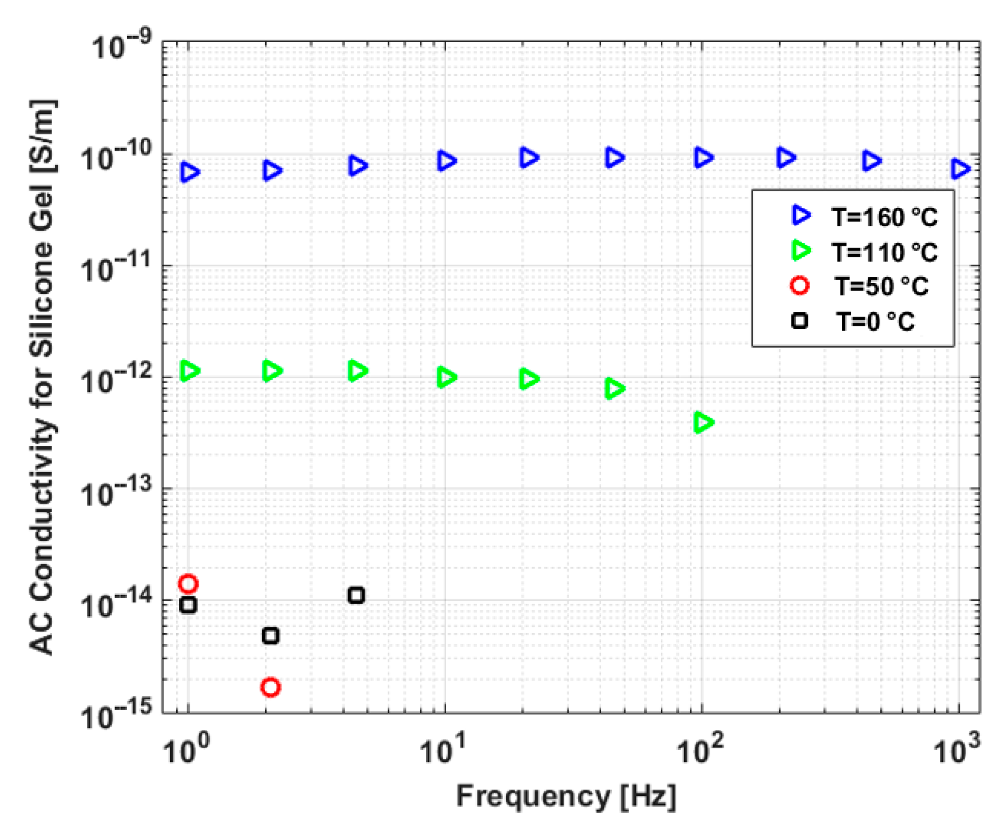
There are rare experimental data about the thermal and frequency dependence of ε r and σ a c of silicone gel reported in the literature. Figure 1 and Figure 2 show the frequency dependence of ε r and σ a c , respectively, of silicone gel at several temperatures between 20 and 160 °C, reproduced from [43] and used in this paper for simulations. The commercial silicone gel was used for experiments. Plate-to-plate electrodes with a gap distance of 1 mm, assuring a uniform electric field within the sample, were used. The electrodes were immersed in silicone gel under a vacuum for about 1 h to remove trapped gas bubbles just before the polymerization.
Simulations are performed for a base case ({22 °C, 50 Hz}) and four case studies (Case 1: {110 °C, 450 Hz}, Case 2: {110 °C, 1000 Hz}, Case 3: {160 °C, 450 Hz} and Case 4: {160 °C, 1000 Hz}). From Figure 1, ε r for the base case and Cases 1–4 are 2.72, 2.29, 2.29, 2.05, and 2.05, respectively. As seen from Figure 1, ε r is frequency-independent for the 50-1000 Hz range, but it decreases with temperature. From Figure 2, σ a c for the base case and Cases 1-4 are 1.1 × 10⁻¹⁴, 3.9 × 10⁻¹³, 3.9 × 10⁻¹³, 8.8 × 10⁻¹¹, and 7.4 × 10⁻¹¹ S/m, respectively. For 110 °C, σ a c was measured up to 100 Hz (3.9 × 10⁻¹³ S/m) in [43] as shown in Figure 2. We assume that σ a c for 450 and 1000 Hz is also 3.9 × 10⁻¹³ S/m. For 22 °C, σ a c was reported up to 4.5 Hz (1.1 × 10⁻¹⁴ S/m) in [43] and we assume that for 50, 450 and 1000 Hz, it does not almost change and is 1.1 × 10⁻¹⁴ S/m. From Figure 2, it can be seen that σ a c is almost frequency-independent, thus the assumptions above are acceptable.

2.2. AlN Substrate

There have been very few reports on the high-temperature insulation properties of the ceramic insulating substrate for power modules. In this paper, ε r and σ a c of AlN used for power modules up to a high temperature of 450 ℃ and a high frequency of 10 MHz measured in [44] are used for simulations. In this regard, ( ε r , σ a c (S/m)) for the base case and Cases 1-4 are (9.43, 5 × 10⁻¹¹), (9.62, 1.45 × 10⁻⁹), (9.42, 2.06 × 10⁻⁹), (10.79, 5.76 × 10⁻⁹), and (10.02, 1 × 10⁻⁸) respectively.
Note that since ε r and σ a c in [43] are reported up to 160 ℃ and 1 kHz, we have to do simulations up to those limits.

2.3. Nonlinear FDC material

Polymeric composites using fillers such as SiC, carbon black, or blends of different oxides, e.g., BaTiO3, TiO2, SiO2, Fe3O4, mica, have been used both for end corona protection of motor stator bars and cable accessories for a long time.
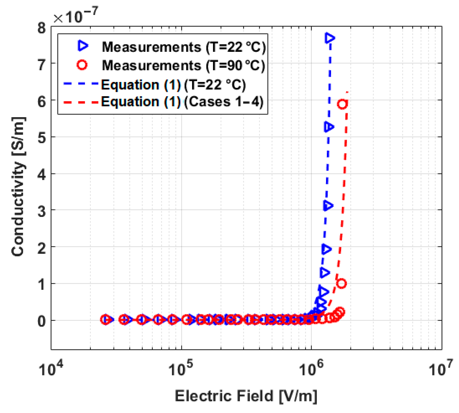
More recently, a new nonlinear field grading material based on ZnO microvaristors has become available and, for the first time, its feasibility for electric field reduction in power modules was studied through simulations [22]. In [45], electrical and thermal data of ZnO microvaristors are presented, where Figure 3 (reproduced from measuring data in [45]) shows the effect of temperature on the conductivity of a silicone compound with ca. 35 vol% ZnO microvaristor filler at 22 and 90 °C. As argued in [45], the combined actions of the thermally activated transport of ZnO microvaristor fillers and the thermal expansion of the silicon rubber matrix result in a rather temperature-independent conductivity.
In this paper, the ZnO microvaristor-silicone compound shown in Figure 3 is considered as nonlinear FDC material for simulations. The measurement data shown in Figure 3 can be fitted by
σ ( E ) = a e b E
where ( a , b ) for 22 and 90 °C are (4.83×10⁻¹², 8.552×10⁻⁶), and (3.092 × 10⁻¹¹, 5.272 × 10⁻⁶), respectively.
The data for 90 °C in Figure 3 are used for the case studies considered in this paper for 110 and 160 °C, since as seen in Figure 3 and argued in [45], conductivity of the ZnO microvaristor-silicone compound is rather temperature-independent. It is also reported that ε r only weakly depends on a frequency above 50 Hz and it is 11.47, 11.18, and 11.11 for 50, 450 and 1000 Hz, respectively [45]. The frequency-dependency of resistivity and temperature-dependency of ε r for microvaristor-silicone compounds are not reported in [45] and we could also not find such data in other literature. Thus, the conductivity and ε r of the microvaristor-silicone compound considered for simulations are assumed to be frequency-independent and temperature-independent, respectively. Thus, for Cases 1–4, ( a ,   b ) from (1) is 3.092 × 10⁻¹¹, 5.272 × 10⁻⁶. ε r for the base case and Cases 1–4 is 11.47, 11.18, 11.11, 11.18, and 11.11, respectively.

3. Modeling and Simulation Results

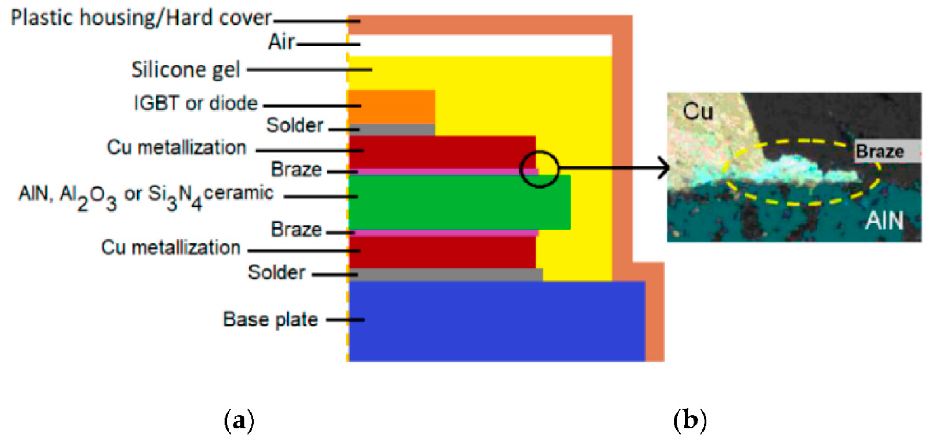
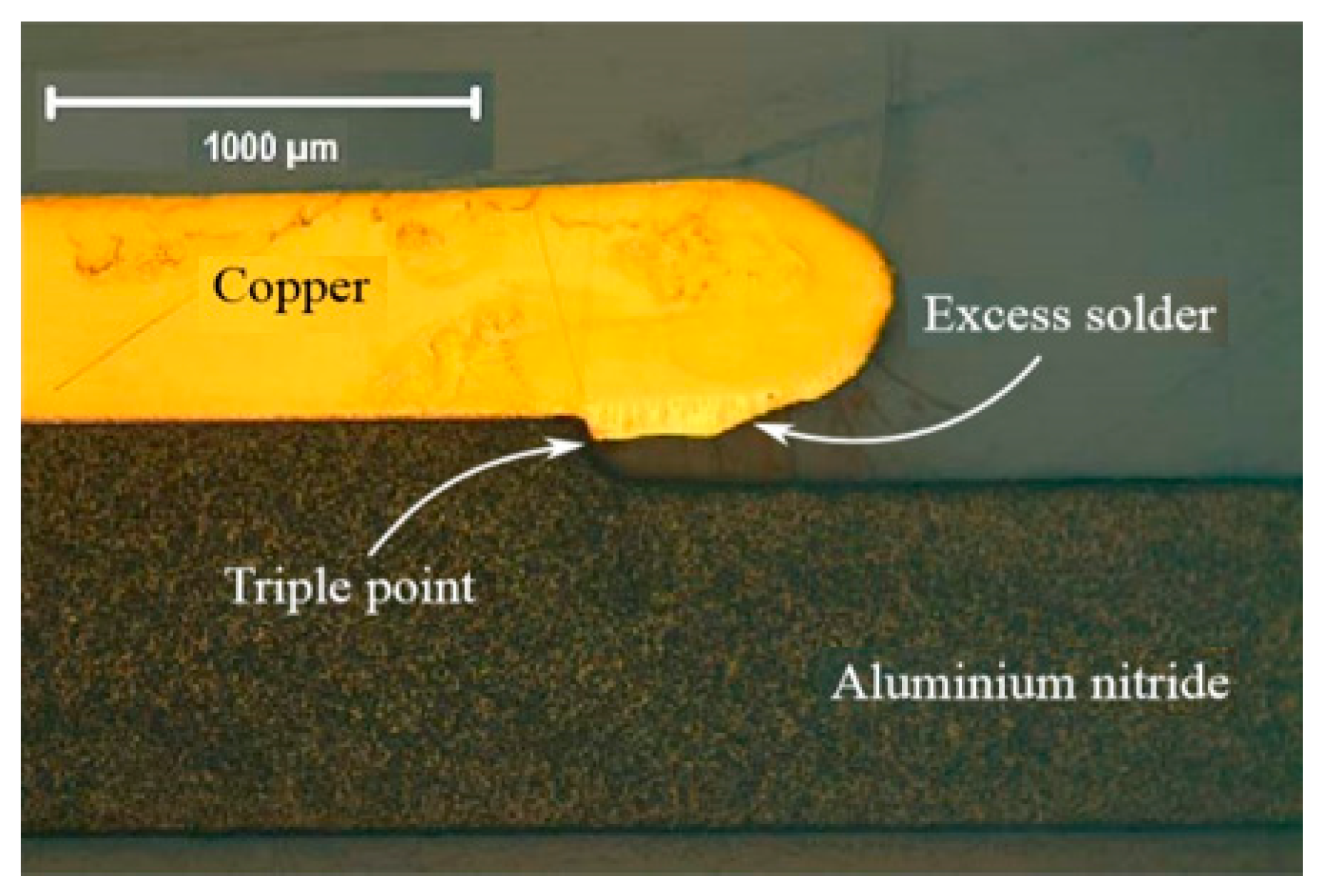
Figure 4 shows the schematic cross-section of a metalized AlN substrate that is the established insulation technology for current power module packaging. However, weak points including sharp edges of the metallizations, protrusions formed by active metal brazing of the copper layers, and triple points where silicone gel, AlN, and copper layers meet, can induce enhanced local electric stress.
The advantage of the protruding substrate introduced in [18] and shown in Figure 5 is that the sharp edges of the metallization layers have been rounded, and also that the triple point has been moved to a region with less electric stress by soldering the copper metallization on a ceramic substrate with the specific height and width of the protrusion.
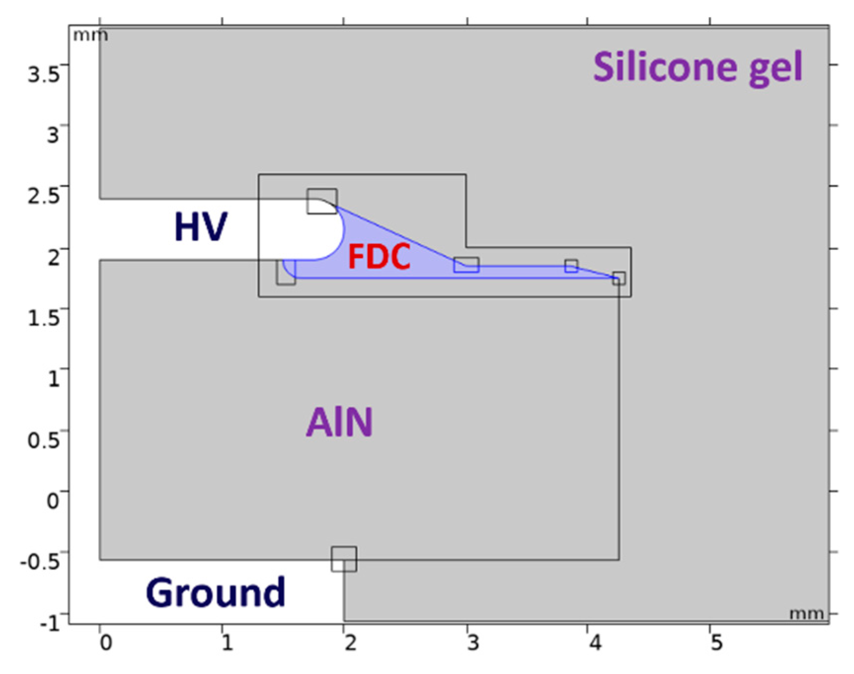
Despite the noticeable electric field reduction within the ceramic substrate through the protruding substrate, a negligible improvement in the electric field distribution within the silicone gel is yielded. To address the enhanced local electric stress within the silicone gel, a nonlinear FDC layer as shown in Figure 6 is applied to high-stressed regions, including the high voltage metallization edges and the rims of the ceramic substrate close to the high voltage zone. Nonlinear FDC materials influence the electric field distribution in the module by increasing the leakage current within the module when the electric stress exceeds a threshold value.
To study the influence of temperature and frequency on the electric field distribution of a 6.5 kV power module benefitting from a protruding substrate combined with the application of a non-bridging nonlinear FDC layer, the geometry shown in Figure 6 is modeled in COMSOL Multiphysics.
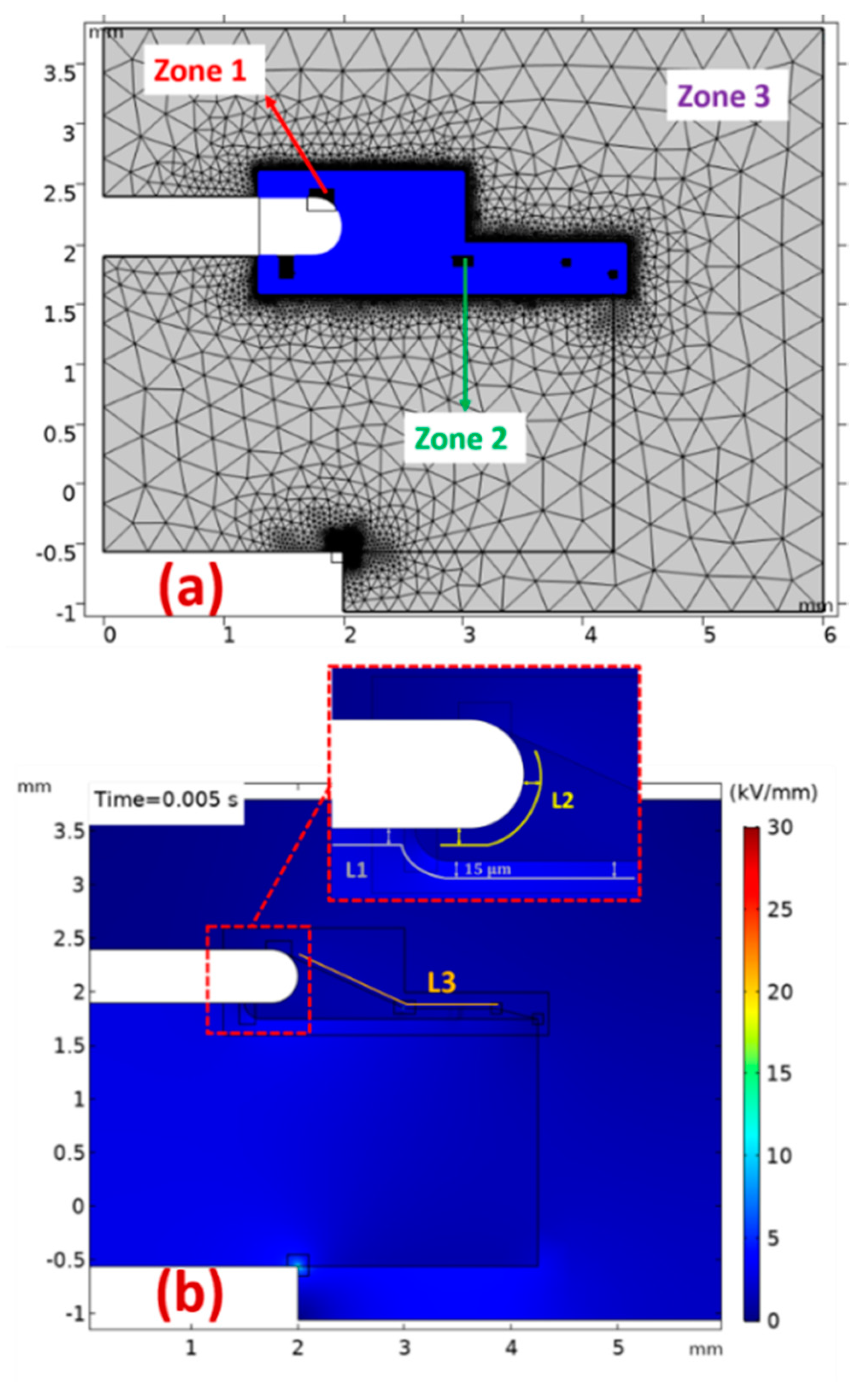
The accuracy of the simulation results in finite element methods (FEMs) is highly dependent on the mesh resolution considered. The higher the density of the mesh elements, the more accurate and reliable the simulation results. However, using an extremely high-resolution meshing for the whole geometry results in a need for lots of memory resources and time-consuming simulations. To address the aforementioned issue, three zones (as shown in Figure 7a) with different mesh sizes were defined. An extremely dense meshing with a maximum element size of 4 µm was used for zone 1, which incorporated all sharp edges. The maximum mesh element sizes of 10 and 400 µm were also used for zones 2 and 3, respectively.
Another parameter that affects the accuracy of the simulation results is the mesh dependency of the electric field at the regions close to the sharp edges and material boundaries. Thus, to address this issue, the electric field measurements are carried out at measuring lines L1 (in AlN substrate), L2 (in nonlinear FDC layer), and L3 (in silicone gel), as shown in Figure 7b, where the lines have a minimum distance of 15 µm from interfaces.
The simulations were carried out for a WBG power module with a blocking voltage of 6.5 kV. According to IEC 61287-1 for PD measurements, a 50/60 Hz voltage with a peak of 1.1 U b , where U b is the blocking voltage of the power module, must be applied to the top metallization, while the bottom metallization layer is grounded. Thus, to simulate the real PD test condition, a 50 Hz AC voltage with a maximum amplitude of 7.15 kV was applied to the HV electrode. However, for Cases 1–4, in which the frequency is higher than 50 Hz, we followed the same procedure as the standard test for PD, by only changing the frequency of the applied voltage from 50 to 450 Hz in Cases 1 and 3, and to 1 kHz in Cases 2 and 4. The electrical parameters discussed in Section 2 were used for the simulations. The maximum value of E , E m a x , along L1–L3 for case studies is presented in Table 1.
As seen in Table 1, the electric field reduction method as the protruding substrate design combined with the application of a nonlinear FDC layer is almost temperature- and frequency-independent in the 22–160 °C and 50–1000 Hz range.
The model and method developed in Section 3, and the measurement data used in Section 2, can be used for power modules with various blocking voltages and other geometrical electric field reduction techniques and especially for practical designs and applications.

4. Conclusions

In practice, the insulation materials of envisaged WBG power modules are exposed to square wave voltage pulses with a frequency up to a few kHz and temperatures up to a few hundred degrees. Temperature and frequency are two important factors that usually affect the electrical characteristics (relative permittivity and AC electrical conductivity) of the dielectric materials and they may influence electric field distribution. The electric field simulations and calculations reported in the literature to date ignore the frequency and temperature dependency of ε r and σ a c for the insulating materials used in the power modules. Therefore, there is doubt about the validation of results for high temperatures and high frequencies. This paper addresses this technical gap through:
  • Providing the measurement data of ε r and σ a c reported in different literature for AlN, silicone gel, and a nonlinear FDC material as a base case {22 °C, 50 Hz} and four cases for {110 °C, 450 Hz}, {110 °C, 1000 Hz}, {160 °C, 450 Hz}, and {160 °C, 1000 Hz},
  • Developing a FEM model for electric field calculations in COMSOL Multiphysics, where the successful electric field reduction method developed in our previous studies via protruding substrate combined with the application of a nonlinear FDC layer was used for simulations,
  • Simulations using the model and measurement data described above, where it was found that the effectiveness of our proposed electric field reduction method as protruding substrate combined with the application of a nonlinear FDC layer is not affected.
For further research, ε r and σ a c of AlN, silicone gel, and the ZnO microvaristor-silicone compound are needed to be measured up to a few ten/hundred kHz and high temperatures of up to 250°C, as these are the envisioned conditions for next-generation WBG power modules. Then using the measurement data, the influence of frequency and temperature up to the mentioned ranges can be studied by the method presented in this paper. Another technical gap is that all ε r and σ a c values reported in the literature for different frequencies are under an AC sinusoidal voltage; however, insulating materials within power modules are under square waveforms. We do not know whether or not results will be different under square waveforms.

Author Contributions

The authors contributed equally to this work in all parts. All authors have read and agreed to the published version of the manuscript.

Funding

This work was supported in part by the National Science Foundation under award number NSF-1942540.

Conflicts of Interest

The authors declare no conflict of interest.

References

  1. Advisory Council for Aeronautics Research in Europe. Aeronautics and Air Transport: Beyond Vision 2020 (Towards 2050); Publications Office of the EU: Brussels, Belgium, 2010. [Google Scholar]
  2. Advisory Council for Aeronautics Research in Europe. Strategic Research & Innovation Agenda-2017 Update; ACARE: Brussels, Belgium, 2017. [Google Scholar]
  3. Roboam, X.; Sareni, B.; Andrade, A.D. More Electricity in the Air: Toward Optimized Electrical Networks Embedded in More-Electrical Aircraft. IEEE Ind. Electron. Mag. 2012, 6, 6–17. [Google Scholar] [CrossRef] [Green Version]
  4. Majumdar, G.; Oomori, T. Some Key Researchers on SiC Device Technologies and Their Predicted Advantages. Power Semicond. 2009, 6, 18–22. [Google Scholar]
  5. Hornberger, J.M.; Mounce, S.D.; Schupbach, R.M.; Lostetter, M.A.B.; Mantooth, H.A. High-temperature Silicon Carbide (SiC) power switches in multichip power module (MCPM) applications. In Proceedings of the IEEE Industry Applications Conference, Kowloon, Hong Kong, China, 2–6 October 2005; pp. 393–398. [Google Scholar]
  6. Schulz-Harder, J. Review of highly integrated solutions for power electronic devices. In Proceedings of the IEEE International Conference on Integrated Power Electronics Systems, Nuremberg, Germany, 11–13 March 2008; pp. 1–7. [Google Scholar]
  7. Tolbert, L.M.; Zhang, H.; Ozpineci, B.; Chinthavali, M.S. SiC-based power converters. In Proceedings of the MRS Spring Meeting, San Francisco, CA, USA, 24–28 March 2008. [Google Scholar]
  8. Liu, G.; Xu, F.; Xu, Z.; Zhang, Z.; Tang, G. Assembly HVDC Breaker for HVDC Grids with Modular Multilevel Converters. IEEE Trans. Power Electron. 2017, 32, 931–941. [Google Scholar] [CrossRef]
  9. Cuzner, R.M. Power electronics packaging challenges for future warship applications. In Proceedings of the IEEE International Workshop on Integrated Power Packaging (IWIPP), Chicago, IL, USA, 3–6 May 2015; pp. 5–8. [Google Scholar]
  10. Bhattacharya, S. Wide-band Gap (WBG) devices enabled MV power converters for utility applications—Opportunities and challenges. In Proceedings of the IEEE Workshop on Wide Bandgap Power Devices and Applications, Knoxville, TN, USA, 13–15 October 2014. [Google Scholar]
  11. Cole, Z.; Stabach, J.; Falling, G.; Killeen, P.; McNutt, T.; Passmore, B. The design and development of a 15 kV SiC half-bridge multi-chip power module for medium voltage applications. In Proceedings of the International Conference on Microelectronics, Doha, Qatar, 14–17 December 2014. [Google Scholar]
  12. Eyer, J.; Corey, G. Energy Storage for the Electricity Grid: Benefits and Market Potential Assessment Guide; Sandia Report no. SAND2010–0815; Sandia National Laboratories: Albuquerque, NM, USA, February 2010. [Google Scholar]
  13. Choi, U.M.; Blaabjerg, F.; Munk-Nielsen, S.; Jorgensen, S.; Rannestad, B. Condition monitoring of IGBT module for reliability improvement of power converters. In Proceedings of the IEEE Transportation Electrification Conference and Expo, Asia-Pacific (ITEC Asia-Pacific), Busan, Korea, 1–4 June 2016; pp. 602–607. [Google Scholar]
  14. U.S. Department of Energy, Electricity Delivery and Energy Reliability. Power Electronics Research and Development, Program Plan; Office of Electricity: Washington, DC, USA, 2011.
  15. Ghassemi, M. Accelerated Insulation Aging due to Fast, Repetitive Voltages: A Review Identifying Challenges and Future Research Needs. IEEE Trans. Dielectr. Electr. Insul. 2019, 26, 1558–1568. [Google Scholar] [CrossRef]
  16. Ghassemi, M. Geometrical techniques for electric field control in (ultra) wide bandgap power electronics modules. In Proceedings of the IEEE Electrical Insulation Conference (EIC), San Antonio, TX, USA, 17–20 June 2018; pp. 589–592. [Google Scholar]
  17. Bayer, C.F.; Baer, E.; Waltrich, U.; Schtetz, A. Simulation of the Electric Field Strength in the Vicinity of Metallization Edges on Dielectric Substrates. IEEE Trans. Dielectr. Electr. Insul. 2015, 22, 257–265. [Google Scholar] [CrossRef]
  18. Reynes, H.; Buttay, C.; Morel, H. Protruding ceramic substrates for high voltage packaging of wide bandgap semiconductors. In Proceedings of the IEEE Workshop on Wide Bandgap Power Devices and Appl. (WiPDA), Albuquerque, NM, USA, 30 October–1 November 2017; pp. 404–410. [Google Scholar]
  19. Muslim, D.J.; Lesaint, O.; Hanna, R.; Reboud, J.L.; Sinisuka, N.I. Electrical characterization of Dibenzyltoluene liquid at high temperatures up to 350°C. In Proceedings of the IEEE Annu. Rep. Conf. Electr. Insul. Dielectr. Phenom. (CEIDP), Cancun, Mexico, 21–24 October 2018; pp. 58–61. [Google Scholar]
  20. Muslim, J.; Lesaint, O.; Hanna, R.; Sinisuka, N.I. Streamer generation and propagation in Dibenzyltoluene and Ester liquids under high temperature. In Proceedings of the IEEE International Conference Dielectr. Liquids (ICDL), Roma, Italy, 23–27 June 2019; pp. 1–4. [Google Scholar]
  21. Muslim, J.; Lesaint, O.; Hanna, R.; Sinisuka, N.I. Partial discharge measurements on Dibenzyltoluene for high temperature encapsulant application up to 350°C. In Proceedings of the IEEE International Conference Dielectr. Liquids (ICDL), Roma, Italy, 23–27 June 2019; pp. 1–4. [Google Scholar]
  22. Donzel, L.; Schuderer, J. Nonlinear Resistive Electric Field Control for Power Electronic Modules. IEEE Trans. Dielectr. Electr. Insul. 2012, 19, 955–959. [Google Scholar] [CrossRef]
  23. Wang, N.; Cotton, I.; Robertson, J.; Follmann, S.; Evans, K.; Newcombe, D. Partial Discharge Control in a Power Electronic Module Using High Permittivity Non-linear Dielectrics. IEEE Trans. Dielectr. Electr. Insul. 2010, 17, 1319–1326. [Google Scholar] [CrossRef]
  24. Ghassemi, M. PD Measurements, Failure Analysis, and Control in High Power IGBT Modules. High Volt. 2018, 3, 170–178. [Google Scholar] [CrossRef]
  25. Ghassemi, M. Electrical Insulation Weaknesses in Wide Bandgap Devices. In Simulation and Modelling of Electrical Insulation Weaknesses in Electrical Equipment; Albarracin, R., Ed.; IntechOpen: London, UK, 2018; pp. 129–149. [Google Scholar]
  26. Tousi, M.M.; Ghassemi, M. Electric field control by nonlinear field dependent conductivity dielectrics characterization for high voltage power module packaging. In Proceedings of the IEEE International Workshop on Integrated Power Packaging (IWIPP), Toulouse, France, 24–26 April 2019; pp. 54–58. [Google Scholar]
  27. Tousi, M.M.; Ghassemi, M. Nonlinear field dependent conductivity materials for electric field control within next-generation wide bandgap power electronics modules. In Proceedings of the 2019 IEEE Electrical Insulation Conference (EIC), Calgary, AB, Canada, 16–19 June 2019; pp. 63–66. [Google Scholar]
  28. Tousi, M.M.; Ghassemi, M. The effect of type of voltage (sinusoidal and square waveform) and the frequency on the performance of nonlinear field-dependent conductivity coatings for electric field control in power electronic modules. In Proceedings of the IEEE Conference on Electrical Insulation and Dielectric Phenomena (CEIDP), Richland, DC, USA, 20–23 October 2019; pp. 601–604. [Google Scholar]
  29. Tousi, M.M.; Ghassemi, M. Electrical insulation packaging for a 20 kV high density wide bandgap power module. In Proceedings of the IEEE Energy Conversion Congress & Exposition (ECCE), Baltimore, MD, USA, 29 September–3 October 2019; pp. 4162–4166. [Google Scholar]
  30. Tousi, M.M.; Ghassemi, M. Nonlinear resistive electric field grading in high-voltage, high-power wide bandgap power module packaging. In Proceedings of the IEEE Energy Conversion Congress & Exposition (ECCE), Baltimore, MD, USA, 29 September–3 October 2019; pp. 7124–7129. [Google Scholar]
  31. Tousi, M.M.; Ghassemi, M. Combined Geometrical Techniques and Applying Nonlinear Field Dependent Conductivity Layers to Address the High Electric Field Stress Issue in High Voltage High-Density Wide Bandgap Power Modules. IEEE Trans. Dielectr. Electr. Insul. 2020, 27, 305–313. [Google Scholar] [CrossRef]
  32. Tousi, M.M.; Ghassemi, M. Characterization of Nonlinear Field Dependent Conductivity Layer Coupled with Protruding Substrate to Address High Electric Field Issue within High Voltage High-Density Wide Bandgap Power Modules. IEEE J. Emerg. Sel. Top. Power Electron. 2020, 8, 343–350. [Google Scholar] [CrossRef]
  33. Nomura, T.; Ikeda, N.; Yoshida, S. Switching Characteristics of GaN HFETs in a Half Bridge Package for High Temperature Applications. IEEE Trans. Power Electron. 2008, 23, 692–697. [Google Scholar] [CrossRef]
  34. Hornberger, J.; Lostetter, A.B.; Olejniczak, K.J.; McNutt, T.; Lal, S.M.; Mantooth, A. Silicon-carbide (SiC) semiconductor power electronics for extreme high-temperature environments. In Proceedings of the IEEE Aerospace Conference Proceedings, Big Sky, MT, USA, 6–13 March 2004; pp. 2538–2555. [Google Scholar]
  35. Frey, D.; Schanen, J.L.; Auge, J.; Lesaint, O. Electric field investigation in high voltage power modules using finite element simulations and partial discharge measurements. In Proceedings of the IEEE 38th Industry Applications Society (IAS) Meeting, Salt Lake City, USA, 12–16 October 2003; pp. 1000–1005. [Google Scholar]
  36. Frey, D.; Schanen, J.L.; Auge, J.L.; Lesaint, O. Electric field investigation in IGBT power modules. In Proceedings of the IEEE International Conference on Solid Dielectrics (ICSD), Toulouse, France, 5–9 July 2004; pp. 864–867. [Google Scholar]
  37. Bayer, C.F.; Waltrich, U.; Soueidan, A.; Baer, E.; Schletz, A. Partial discharges in ceramic substrates - correlation of electric field strength simulations with phase resolved partial discharge measurements. In Proceedings of the IEEE International Conference on Electronics Packaging (ICEP), Sapporo, Japan, 20–22 April 2016; pp. 530–535. [Google Scholar]
  38. Waltrich, U.; Bayer, C.F.; Reger, M.; Meyer, A.; Tang, X.; Schletz, A. Enhancement of the partial discharge inception voltage of ceramic substrates for power modules by trench coating. In Proceedings of the IEEE International Conference on Electronics Packaging (ICEP), Sapporo, Japan, 20–22 April 2016; pp. 536–541. [Google Scholar]
  39. Hourdequin, H.; Laudebat, L.; Locatelli, M.; Bidan, P. Design of packaging structures for high voltage power electronics devices: Electric field stress on insulation. In Proceedings of the IEEE International Conference on Dielectrics (ICD), Montpellier, France, 3–7 July 2016; pp. 999–1002. [Google Scholar]
  40. Hourdequin, H.; Laudebat, L.; Locatelli, M.L.; Valdez-Nava, Z.; Bidan, P.; Razek, A. Metallized Ceramic Substrate with Mesa Structure for Voltage Ramp-up of Power Modules. Eur. Phys. J. Appl. Phys. 2019, 87, 20903. [Google Scholar] [CrossRef] [Green Version]
  41. Deshpande, A.; Luo, F.; Iradukunda, A.; Huitink, D.; Boteler, L. Stacked DBC cavitied substrate for a 15-kV half-bridge power module. In Proceedings of the IEEE International Workshop on Integrated Power Packaging (IWIPP), Toulouse, France, 24–26 April 2019; pp. 12–17. [Google Scholar]
  42. Valdez-Nava, Z.; Kenfaui, D.; Locatelli, M.; Laudebat, L.; Guillemet, S. Ceramic substrates for high voltage power electronics: past, present and future. In Proceedings of the IEEE International Workshop on Integrated Power Packaging (IWIPP), Toulouse, France, 24–26 April 2019; pp. 91–96. [Google Scholar]
  43. Do, M.T.; Augé, J.-L.; Lesaint, O. Dielectric losses and breakdown in silicone gel. In Proceedings of the IEEE Annu. Rep. Conf. Electr. Insul. Dielectr. Phenom. (CEIDP), Kansas City, MO, USA, 15–18 October 2006; pp. 541–544. [Google Scholar]
  44. Abe, T.; Suenaga, M.; Imakiire, A.; Kozako, M.; Hikita, M.; Shiota, H.; Nishimura, T.; Muto, H. Dielectric properties and partial discharge inception voltage of Aluminum Nitride insulating substrate at high temperatures. In Proceedings of the IEEE International Conference on Integrated Power Electronics Systems (CIPS), Stuttgart, Germany, 5 July 2018; pp. 155–160. [Google Scholar]
  45. Donzel, L.; Greuter, F.; Christen, T. Nonlinear Resistive Electric Field Grading Part 2: Materials and Applications. IEEE Electr. Insul. Mag. 2011, 27, 18–29. [Google Scholar] [CrossRef]
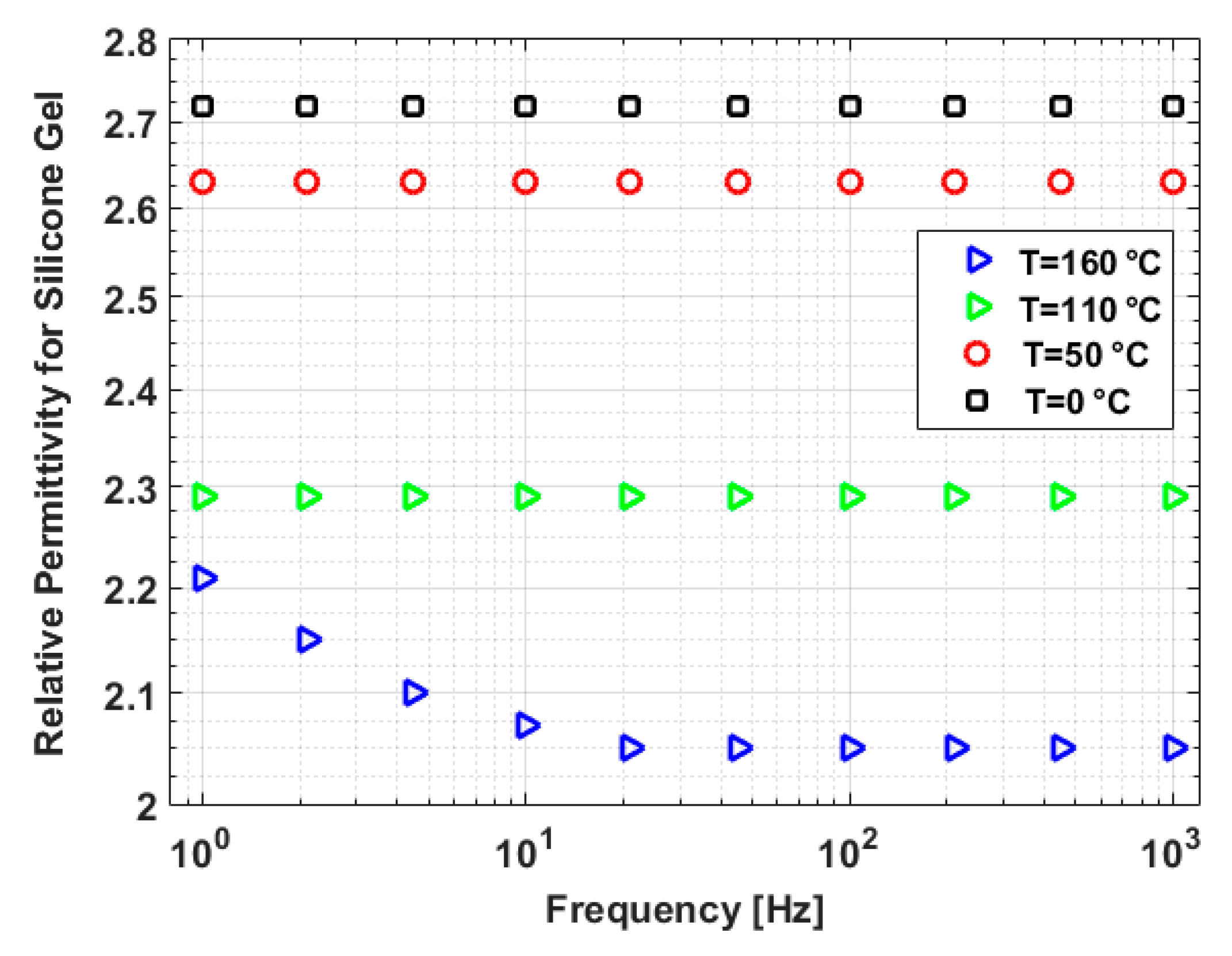
Figure 1. Frequency dependence of the relative permittivity of silicone gel at several temperatures between 20 and 160 °C, reproduced from [43].
Energies 13 02022 g001
Figure 2. AC conductivity of silicone gel versus frequency at several temperatures between 20 and 160 °C, reproduced from [43].
Energies 13 02022 g002
Figure 3. σ ( E ) of a ZnO microvaristor-silicone compound for different temperatures, reproduced from [45].
Energies 13 02022 g003
Figure 4. (a) Schematic cross-section of a metalized aluminum nitride (AlN) substrate, (b) Protrusion with extremely sharp edges of brazing below the metallization.
Energies 13 02022 g004
Figure 5. Cross-section of the protruding substrate, reproduced from [18].
Energies 13 02022 g005
Figure 6. The geometry considered for simulations.
Energies 13 02022 g006
Figure 7. (a) Meshing strategy, (b) electric field distribution for the geometry considered according to Figure 6 under a 7.15 kV (peak) AC 50 Hz voltage.
Energies 13 02022 g007
Table 1. E m a x at L1–L3 for the geometry of Figure 6 for the base case and Cases 1–4.
CaseL1 (kV/mm)L1 (kV/mm)L3 (kV/mm)
Base case3.911.173.49
Case 13.881.842.21
Case 23.901.722.26
Case 33.851.862.22
Case 43.901.982.34