Article

A Novel Space Vector Modulation Scheme for a 10-Switch Converter

by
Parviz Najafi
1,*,
Abbas Houshmand Viki
1,
Mahdi Shahparasti
2,
S. Sajjad Seyedalipour
1 and
Edris Pouresmaeil
3,*
1
Electrical Engineering Department, Khajeh Nasir Toosi University of Technology, Tehran 19697-64499, Iran
2
Electrical Engineering Section, The Mads Clausen Institute, University of Southern Denmark, 5230 Odense, Denmark
3
Department of Electrical Engineering and Automation, Aalto University, 02150 Espoo, Finland
*
Authors to whom correspondence should be addressed.
Energies 2020, 13(7), 1855; https://doi.org/10.3390/en13071855
Submission received: 17 February 2020 / Revised: 21 March 2020 / Accepted: 7 April 2020 / Published: 10 April 2020
(This article belongs to the Section F: Electrical Engineering)

Abstract

:
Three-level converters have drawn extensive attention due to their ability to deliver high-quality power. High semiconductor count is the main drawback of three-level converters. As a solution to this, a 10-switch converter is presented, that has advantages over both two- and three-level converters, simultaneously, plus it is applicable to a variety of power ranges. However, the switching pattern of 10-switch converter is not as simple as standard three-level converter due to lack of medium vectors. This paper presents a novel space vector modulation (SVM) for a 10-switch converter to reduce total harmonic distortion (THD) and common mode voltage (CMV) of this converter in comparison to prior carrier-based modulation methods. A simplified, low-cost modulation algorithm for the converter is proposed. The designed switching sequence has aimed at a low output THD and enhancement of DC bus voltage utilization. The performance of the proposed SVM is then compared to upgraded sinusoidal PWM. AC power quality and CMV of a 10-switch converter based on two modulation methods are investigated via simulation models. It was validated via simulation and experimental models that the proposed SVM utilized DC bus voltage more efficiently, generated remarkably less THD compared to other methods, and had a lower peak and rms CMV.

1. Introduction

The interest in using multilevel converters in energy conversion for renewable energy resources application in microgrids, electric drives, plug-in electric vehicles, etc. is rapidly growing [1,2,3,4,5]. Two-level converters are the standard solution of the industry to satisfy the mentioned application requirements, and these converters have a massive market share because of their simple control and performance. However, insufficient efficiency in comparison to multilevel converters and high power loss in high switching frequencies are the main difficulties with these converters [6]. The appealing advantages of multilevel converters include their high efficiency in specific switching frequencies and high power quality, making them a proper choice for the mentioned applications [7]. However, the high semiconductor count of multilevel converters is accounts for a significant disadvantage in large scale production [8]. Therefore, the neutral point clamped (NPC) converter is a standard candidate of three-level multilevel converters that has high quality AC outputs and low semiconductor number comparing to other multilevel topologies. However, the semiconductor number in the NPC converter is twice as many as the three-phase two-level converter, and it requires six additional fast diodes in its topology.
A three-level T-type converter is introduced as a solution for high semiconductor count challenge of multilevel converters that omits six fast diodes in comparison to NPC converter topology. A T-type converter profits the advantages of two-level converters plus the voltage quality of three-level converters [9]. However, the main drawback of this converter type is the voltage stress on IGBTs that is equal to the total DC-link voltage. This means that two-times higher rate semiconductor has to be selected for a three-level T-type converter in comparison to a neutral point clamped (NPC) converter. A three-level T-type converter employs 12 IGBTs and eliminates six extra fast diodes used in NPC topology. The reduction of fast diode number and choosing higher rate semiconductors are the main advantages and disadvantages of T-type converter’s structure.
A new class of converter in the matter of reducing the semiconductor count and elevating AC and DC voltage quality is introduced in [10], which is a hybrid 2/3 level converter called a 10-switch converter. Structurally, it resolves high semiconductor count in comparison to three-level converters such as NPC and T-type. However, its topology cannot produce a full three-level AC voltage and delivers a mixture of two- and three-level AC voltages. Similar to the T-type converter, it basically combines the positive aspects of the two-level converter. Although regarding the reduction of semiconductors, this converter type reduces two switches in comparison to T-type, furthermore, unlike NPC, its topology does not need any separate fast diodes. Moreover, the 10-switch converter’s voltage stress on IGBTs is a combination of half and total DC-link voltages, which means that voltage stress of auxiliary leg semiconductors is similar to NPC converter which is equal to half of the DC-link voltage. For the rest of semiconductors, this will be equal to the total DC-link voltage, which is the same as two-level and three-level T-type converters. Concerns about heat dissipation in the additional auxiliary leg of a 10-switch converter and the capacitor size of a DC-link converter are resolved since the auxiliary leg switches endure half voltage stress in comparison to other semiconductors and the maximum current applied to the semiconductors remain the same in the converter. Also, DC-link capacitor size of this converter is dependent on variables such as maximum allowed voltage ripple and its capacitance calculation is similar to three-level converters which was investigated in [11].
One of the main common features between a 10-switch converter and multilevel converters is the inherent bipolar DC side that widens 10-switch converter's application range. However, Two-level converters have to apply a separate DC/DC converter at the DC side to obtain the bipolar feature. The additional DC/DC converter has its downsides including that the power rate of this additional converter is the same as the three-phase converter, it requires a separate control system, and adds extra costs and volume compared to the former two-level converter.
Previous works on a 10-switch converter are limited to applying sinusoidal pulse width modulation (SPWM) methods to the converter and its applications are not discussed [12]. The carrier-based modulation methods on this converter have high voltage total harmonic distortion (THD) and low-quality output waveforms. Therefore, space vector modulation (SVM) as an acceptable method that inherently reduces the THD compared to SPWM methods and elevates the output quality has to be examined for the 10-switch converter. The voltage vectors in a two-level SVM include two types: zero and active vectors. However, the voltage vectors of a common three-level SVM method are categorized into four types: zero, small, medium, and large vectors [13]. This classification is on the basis of the voltage vector magnitude. In each region of every sector, the nearest three voltage vectors are selected to minimize the transitions of switches and reduce the switching power loss. Due to the structure of a 10-switch converter, a medium voltage vector cannot be produced, since applying a medium voltage vector means that each leg of the three main legs has a different switching state which leads to a short circuit in either of the DC-link poles. Therefore, space vector modulation method of 10-switch converters differs from the three level types. In three-level SVM methods, each sector triangle divides into four equal smaller triangles that form four regions. The adjacent voltage vectors define the switching sequence in that region, however, the absence of a medium voltage vector means that the sectors cannot be divided similarly to three level converters. In the 10-switch converter, each sector can be divided into a small triangle and a trapezoid which contains the three earlier triangles. Thus, designing an SVM method that could work under all modulation indexes and surpasses carrier-based methods in quality is the primary challenge. In [14], a four-vector SVM method is introduced for a Z source converter connected to a 10-switch converter. The simulation results showed inadequate output voltage and unequal currents, which leads to the conclusion that the discussed SVM method for this converter is not quite effective.
In this paper, the superiority of the proposed SVM method on 10-switch converter is analyzed and compared to SPWM methods which are introduced earlier in [10,12,15]. Output quality evaluations of the 10-switch converter are discussed, and common mode voltage (CMV) of the converter is surveyed. Section 2 reveals the main characteristics and features of the 10-switch converter. SPWM and SVM differences are explained in Section 3, and the proposed SVM method is presented afterward. Region determination, dwell time calculations, and switching sequence are described in Section 3 as well. In Section 4, simulations of the proposed SVM and modified SPWM methods are presented, and power quality of converter outputs are evaluated and compared to each other; also, the effectiveness of presented SVM is validated through experimental results.

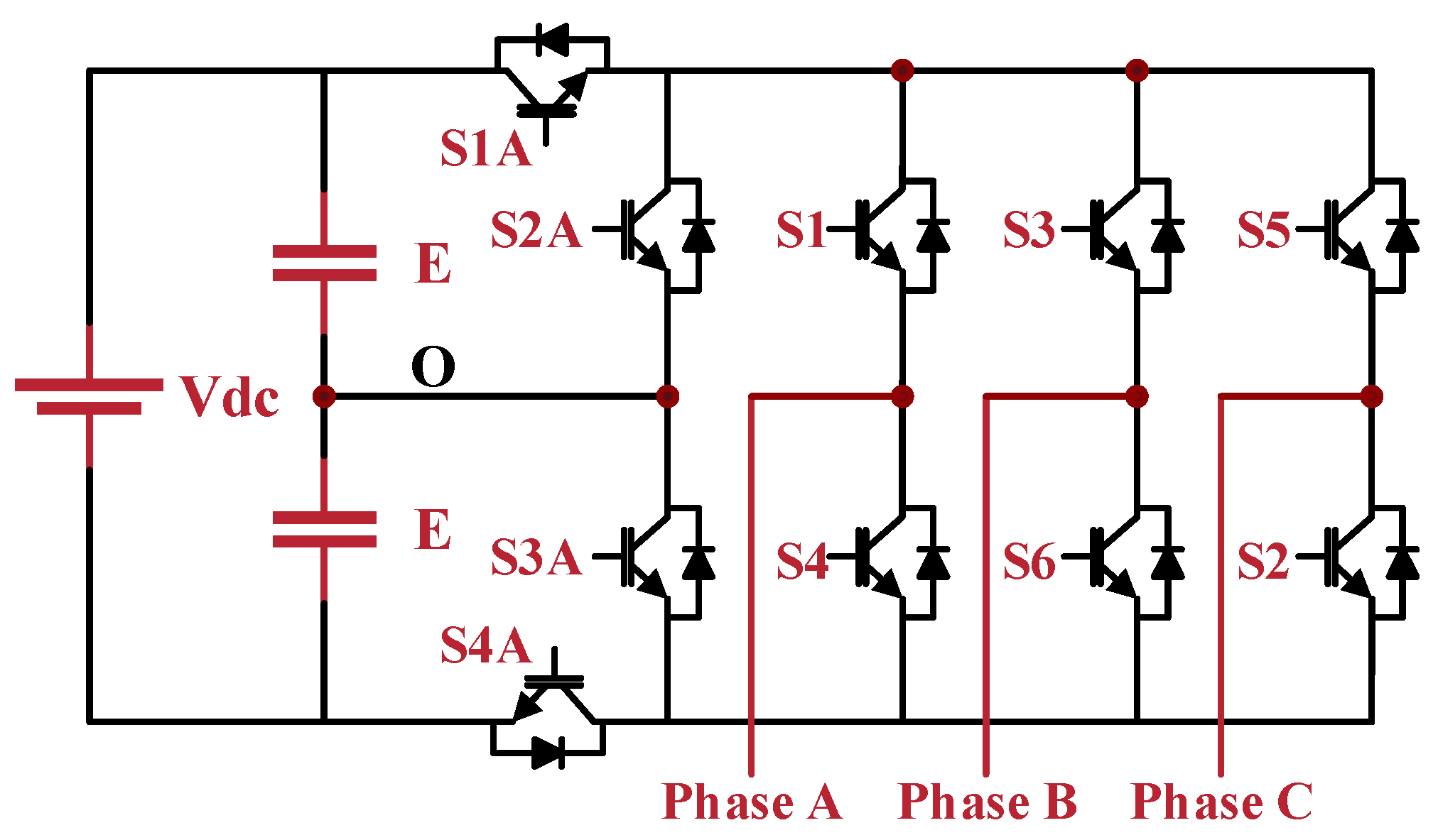
2. Characteristics of a 10-Switch Converter

Figure 1 shows a 10-switch inverter that has a three wire bipolar DC topology with 2/3 level output AC voltage. This inverter is created by adding S1A to S4A switches to the conventional voltage source inverter (VSI). The topology of this inverter contains three main legs and an auxiliary leg composed of four switches that are utilized by other three legs to produce three types of switching states (P, O, and N). Table 1 demonstrates switching states of the 10-switch converter that shows the utilization of auxiliary leg switches by all three main legs. Switching state O means that one of the middle switches in the auxiliary leg is turned on considering the other leg states. If switching state P or N is generated, the auxiliary leg switch S1A or S4A is turned on.

2.1. Evaluation of a 10-Switch Converter Application Based on Available Challenges in Two- and Three-Level Converters

The 10-switch converter is a wise choice for low voltage applications (under 690 V). This converter is suitable for the grid-tied converter, unstoppable power source (UPS), and speed control of permanent magnet motor and induction motor application. Based on [16], three-level converters have multiple advantages in low voltage applications with medium to high switching frequencies over two-level converters, including:
  • The difference in switching loss energies between IGBTs of the same current class and adjacent voltage class is the key factor to reach low switching losses.
  • The three-level converter enables substantially higher switching frequencies applying devices of the same technology and current compared to the two-level converter.
  • The low on-state voltage of IGBTs has higher leverage on three-level converters compared to two-level converters which is an essential factor for calculating the conduction losses.
  • Reduction of the filter size, weight and cost are possible in three-level converters due to their lower voltage harmonics.
  • Reliability concerns in three-level converters can be resolved by appropriate design choices. The reduction of semiconductor losses will help to reduce the average temperature at the components and thus, decrease the failure rate.
  • Application of three-level converters is economically feasible in high energy cost markets, even at low switching frequencies.
The above points are the differences between two- and three-level power converters in low voltage applications which emphasizes on the positive points of the three-level converter. However, concerns about reliability, higher switching loss, and costs still exist, and in order to resolve these challenges, appropriate design choices have to be considered. As a solution, the 10-switch converter can be utilized to satisfy the mentioned challenges, since its topology is a compromise between two and three-level converters.

2.2. The Procedure of Feasible Modulation Methods on a 10-Switch Converter

The first step in carrier-based modulation of the 10-switch inverter is determining the middle signal among the three-phase balanced reference signals that are decided in Equations (1) and (2).
V A r e f = m · cos ( ω s t ) V B r e f = m · cos ( ω s t 2 π / 3 ) V C r e f = m · cos ( ω s t 4 π / 3 )
V m a x = m a x ( v A , r e f , v B , r e f , v C , r e f ) V m i d = m i d ( v A , r e f , v B , r e f , v C , r e f ) V m i n = m i n ( v A , r e f , v B , r e f , v C , r e f )
1 2 + 1 4 V m i d < V r e f < 1 2 + 1 4 V m i d
In the second step, each of these reference signals is tested in Equation (3) to realize the modulation type. If the reference signal of each converter leg satisfies Equation (3), that converter leg has a two-level PWM that means this reference signal will be compared to a triangle signal with an amplitude between –1 and 1. Otherwise, three-level PWM is applied to this leg. The carrier signals of the three-level PWM are two in-phase positive and negative triangle signals which are selected to be compared to the reference signal, considering whether the reference signal has a positive or negative value. It has to be mentioned that not all three legs can have a three-level modulation since the structure of the converter does not allow it. However, all efforts are conducted to maximize the three-level PWM period, in order to achieve high-quality outputs. In the previous efforts [10], the procedure of detecting the middle signal required huge computational steps and each sector of time interval was split in to three intervals. Each interval has its separate switching sequence and equations. The modified SPWM method for the 10-switch converter was introduced to reduce the high computations at each step of the modulation method and omits the need to divide each sector to three intervals and determining the minimum, maximum, and medium signal at every interval.
A comprehensive flowchart of modified SPWM method is described in Figure 2. The flowchart demonstrates that each reference signal’s amplitude is compared to the other two signals which defines whether each leg has two or three-level PWM in order to generate output voltages. Sinusoidal pulse width modulation of 10-switch converter requires high computation steps to determine the maximum, minimum, and middle signal of reference signals in each moment so that based on equations determined in [10], two- or three-level modulation for that specific moment is selected.
From another point of view, a 10-switch converter owns twenty-one switching voltage vectors consisting of eighteen active and three zero vectors (PPP, OOO, and NNN) in comparison to two level VSI and three-level VSI that have eight and twenty-seven switching vectors, respectively. Table 2 demonstrates space vector table of the 10-switch converter which indicates that the 10-switch converter’s active switching vectors and their amplitude are the same as the three-level VSI. Detailed information of all small and large vectors are depicted in Figure 3 and for the sake of brevity, switching state of one small and large vector is described in Table 2. As seen in Table 2, the medium voltage vectors are absent in the vector table of the 10-switch converter. Figure 3 shows the active vectors that construct the space vector diagram of the 10-switch converter in which eighteen active vectors, including six large vectors and twelve small vectors, with three zero vectors are placed at the center of a hexagon.
The dotted line in Figure 3 depicts the hypothetical place of the medium voltage vector which is not available in this converter. The area of the hexagon in the 10-switch inverter is divided into six sectors (I–VI) and each sector is divided into smaller parts. However, lack of medium voltage vectors is shown in Figure 3 which is the difference between the space vector diagram of 10-switch converter and three-level converters. This issue has a widespread direct effect on the converter’s output current and voltage THD, switching patterns and neutral point voltage deviation [13]. The 10-switch converter can work either in inverter or rectifier mode. Assuming that this converter is working in the inverter mode, response of the neutral point voltage to applying a small voltage vector is similar to the three-level inverter, which means neutral point voltage increases when the P-type small vector is used and decreases when the N-type small vector is applied. Applying zero or large vectors does not have an effect on neutral point voltage. On the contrary, using medium vectors in three-level VSIs has an undefined effect on neutral point voltage which makes it difficult to control the deviation of neutral point voltage of such inverters [13].

3. Novel SVM Method for a 10-Switch Converter

A novel modulation technique is presented in this section. This method has aimed to reduce the power loss, neutral point voltage, and THD of converter outputs, and increase the DC-link voltage utilization [17]. In the first step, analogous to space vector methods of three-level VSI, the reference voltage vector is produced, and its amplitude and angle are measured. In the next step, sector and region in which the reference voltage vector ( V r e f ) is located, are determined. As it is demonstrated in Figure 3, regions of each sector are similar to each other. Amplitude and angle of the reference voltage vector specify the region and its related sector in which it is located.

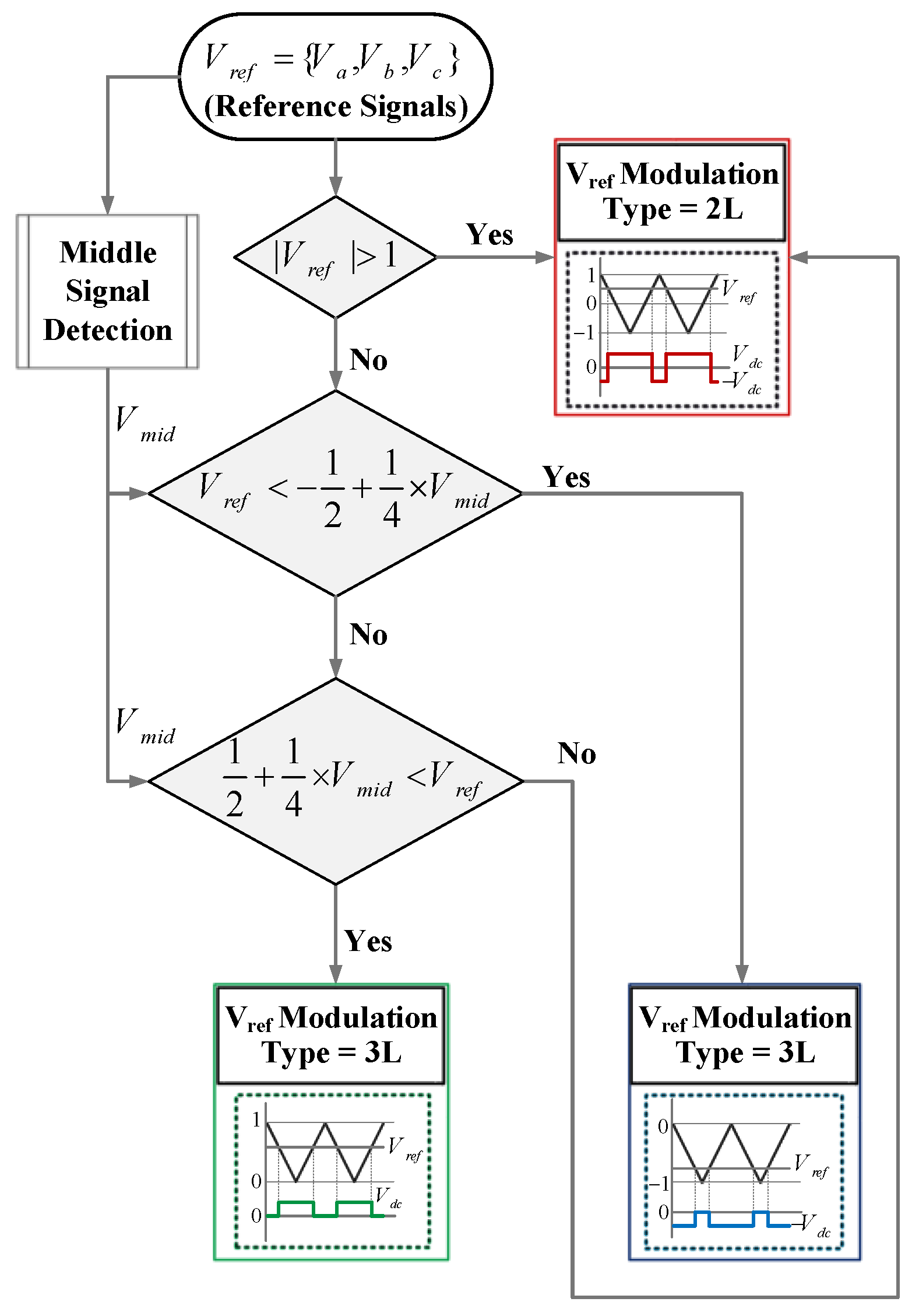
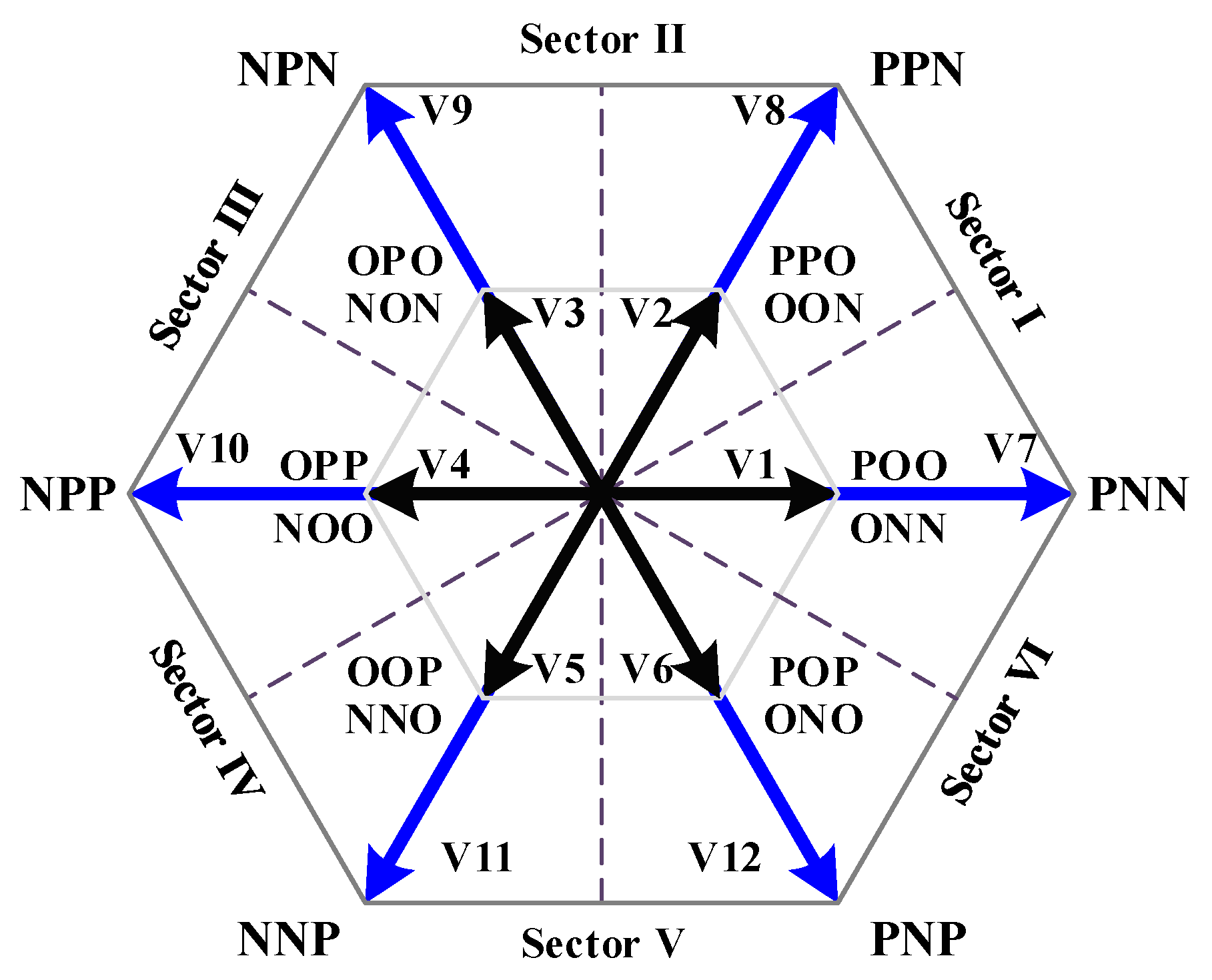
3.1. Region Determination

The procedure that defines each region in the space vector diagram of this converter is dependent on the available voltage vectors for each region and the calculated dwell time for each vector. Lack of medium voltage vectors leads to confusion for vector selection in the highlighted region of Figure 4. It is evident that if the reference voltage is placed in the highlighted region, its vector selection can be the same as region 1, since two small vectors and the zero-voltage vector can construct every possible reference voltage value. If the middle area uses the switching procedure of the first region, a rotating voltage vector with a constant magnitude would continuously change its pattern from using large voltage vectors to using only small vectors, and goes back again to the large vector which leads to increase in the transition of switching states. Alternatively, the highlighted region is shown in Figure 4 can be split in half, and each side gets assigned to the adjacent region. Dividing this area and covering this region via two adjacent regions results in employing two large vectors and the near small vectors that cause a remarkable decrease in the transition of switching states, which is demonstrated in Figure 5.
In order to calculate the region in which V r e f is located, normalized reference voltage vector ( m i ) of the 10-switch inverter is obtained. Reference voltage vector is normalized in the first sector shown in Figure 5 which demonstrates that the maximum modulation index in this converter is 2 / 3 , which is equal to the three-level inverters. Decomposition of the normalized reference voltage vector into zero and sixty degrees’ axes are shown in Figure 5. m 1 and m 2 are the projections of V r e f on the mentioned axes and their value is dependent on the V r e f angle which is represented in Equations (4) and (5). These calculations are valid until over modulation is avoided.
m 1 = m i ( cos θ sin θ 3 )
m 2 = 2 m i ( sin θ 3 )
It is evident from Figure 5 that the maximum value of m 1 and m 2 is equal to 1, and that these variables are dependent on the reference voltage vector’s angle and amplitude. Therefore, determining m 1 and m 2 specifies the region in each sector. Based on Equations (4) and (5), Table 3 obtained, which defines the region in which the reference voltage vector lies. If M i amplitude passes region 1 area, it enters a trapezoid area which is divided into two equal areas by an angle bisector. Therefore, when M i angle exceeds 30 degrees, the region changes from 2 to 3. Trapezoid area is split in half to compensate lack of medium voltage. Each half is switched by the two large voltage vectors and the adjacent small vector.

3.2. Voltage Vector Selection and Dwell Time Calculation

The reference voltage vector is synthesized by three adjacent stationary voltage vectors. Dwell time of these three vectors has to be calculated during a sampling period ( T s ) of the modulation method. Selecting the three nearest voltage vectors in this inverter differs from the three level VSI in all regions except from the first one. In this method, vector selection in region 1 is precisely the same as three-level converters, and for the remaining regions, two large vectors related to that sector with the nearest small vector are chosen. Selecting the nearest small vector means choosing the small vector with the lowest angle difference to the reference vector, which can be P-type or N-type of that small vector.
Selecting two small vectors and the nearest large vector was considered, and related calculations were conducted. It is concluded that in high modulation indexes, a negative dwell time for relative voltage vectors is produced, which is not acceptable. Moreover, choosing two small vectors instead of one, results in the reduction of DC-link voltage utilization and the increase in switching loss.
Another downside of using two small vectors is the redundant states of the small vector, which enhances the switching sequence states, and a seven-segment switching sequence may turn into at least an eleven-segment switching sequence which requires more powerful controllers for computing the dwell time for each state and increases the costs. For the sake of brevity, calculations regarding choosing two small vectors and the nearest large vector are omitted.
Based on the volt-second balancing principle, the product V r e f of T s equals the sum of the voltage multiplied with the time interval of three selected adjacent voltage vectors. As it is depicted in Figure 6, it is assumed that V r e f is located in region 2, where large vectors of this sector are V 7 , V 8 , and the nearest small vector is V 1 . The voltage-second balancing principle for this region is written as Equations (6) and (7).
V r e f T s = V 1 T a + V 7 T b + V 8 T c
T s = T a + T b + T c
From the above equations, the dwell time of voltage vectors is calculated in Equation (8).
T a = 2 T s V r e f T s V d c ( 3 cos θ + 3 sin θ ) T b = 3 V r e f T s V d c ( cos θ ) T s T c = 3 V r e f T s V d c ( sin θ )
By applying the same procedure, the dwelling time of selected voltage vectors in each region of the first sector is obtained, as displayed in Table 4.

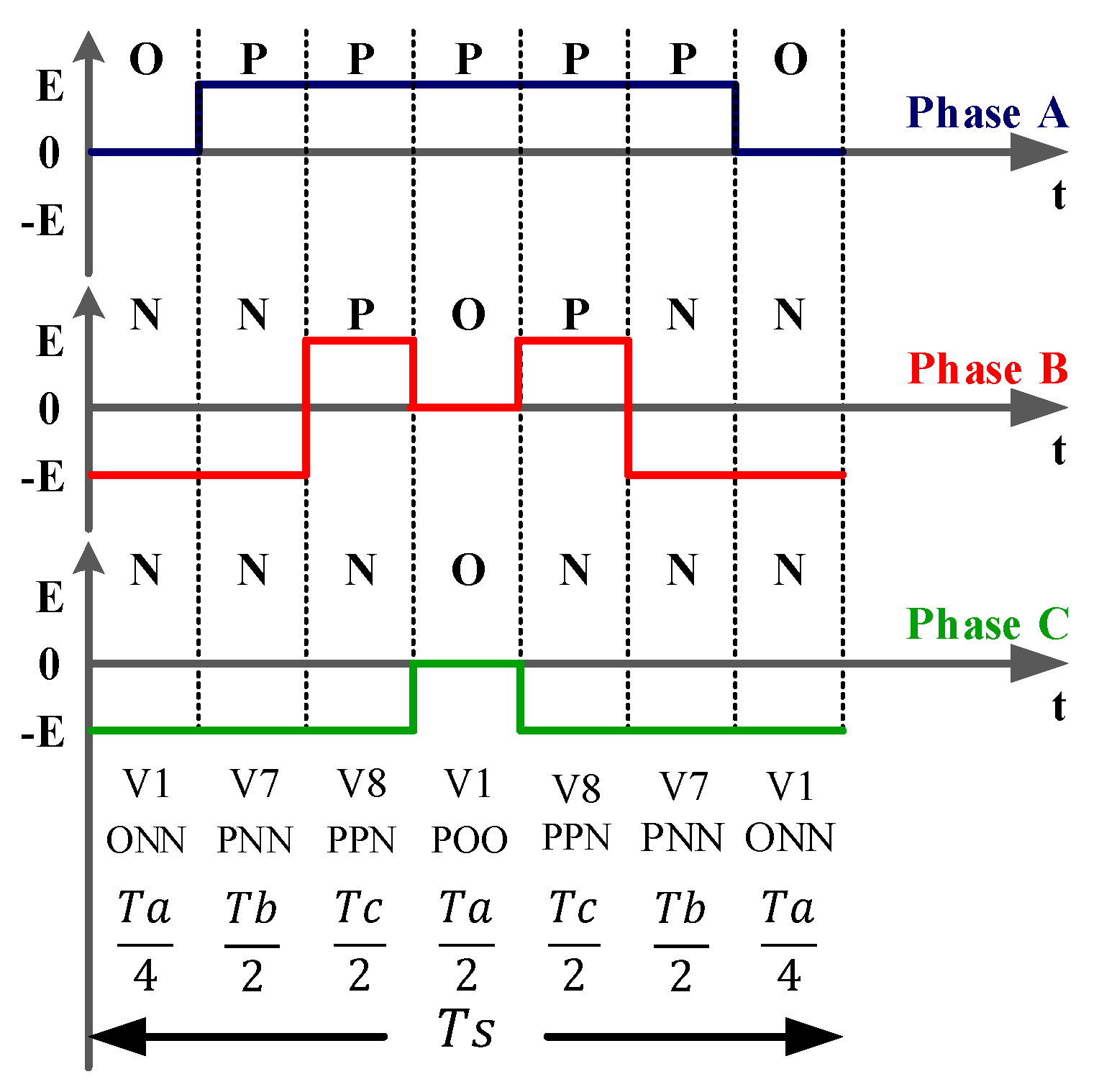
3.3. Symmetrical Switching Sequence

The next step after selecting voltage vectors for each region and calculating their dwell times, is arranging the switching sequence. Redundant switching states result in multiple options to determine a switching sequence. In the proposed method, minimizing the THD is the main objective of arranging the switching sequence. Figure 7 shows an example of a seven segment switching sequence in which T s is divided into seven segments for selected vectors in region two of sector I.
The shape of six sectors and eighteen regions of space vector diagram are identical; therefore, vector selection, dwell time calculation and switching sequence for the remaining sectors have a direct relationship with the first sector. In order to avoid unnecessary procedures and computations in the microcontroller, all calculations of other sectors are carried out the same as sector I. The simple flowchart demonstrated in Figure 8 describes the whole process of the designed SVM. In the first step, the sector of the reference voltage vector is stored, and then the voltage vector is transformed into the first sector which is considered as the reference of calculations. After that, the region and dwell time of voltage vectors are determined. Now, the reference voltage vector is allocated to its original sector and three appropriate dwell times regarding Table 4 are selected for the three selected voltage vectors related to the original sector. Finally, the switching pattern is generated based on the selected voltage vectors.
Enhancing the switching sequence segments and increasing data samples causes lowering the THD level of output waveforms, but it eventually leads to a rise in switching frequency and switching power loss. In order to prove that the decrease of the THD value of output waveforms and the increase of the power quality in the 10-switch converter have not been achieved by increasing the switching sequence segments and enhancing the data samples, the switching sequence of the prior carrier-based modulation method in [10] is compared to the proposed method. Transitions of switch positions are shown in a series at sector I in Table 5. The carrier-based method has three intervals in one sector, and each interval has its specific switching sequence [10], and the modulation of this sector takes place respectively, which means after seven segment of interval 1, segments of interval 2 and 3 occur. Within sector I, 21 segments are needed to perform the carrier-based modulation method.
On the other hand, assuming that the amplitude of the normalized reference voltage vector of the converter is constant, the vector either passes through region 2 and 3, or only goes across region 1. If the vector passes by region 2 and 3, fourteen switching segments are required, and if it goes across region 1, only seven segments are needed. In the worst-case scenario, when the reference vector has pulsating amplitude and passes through all the regions. The segments of the switching sequence will be equal to the carrier-based method. As a result, comparing the two methods and the required segments at the switching sequence of one sector leads to the conclusion that the proposed method optimizes the THD level of converter outputs with less switching segments and does not lead to an increase in the switching frequency. This method is applicable to all converters in which the medium voltage vector is not available, especially hybrid 2/3 level converters.

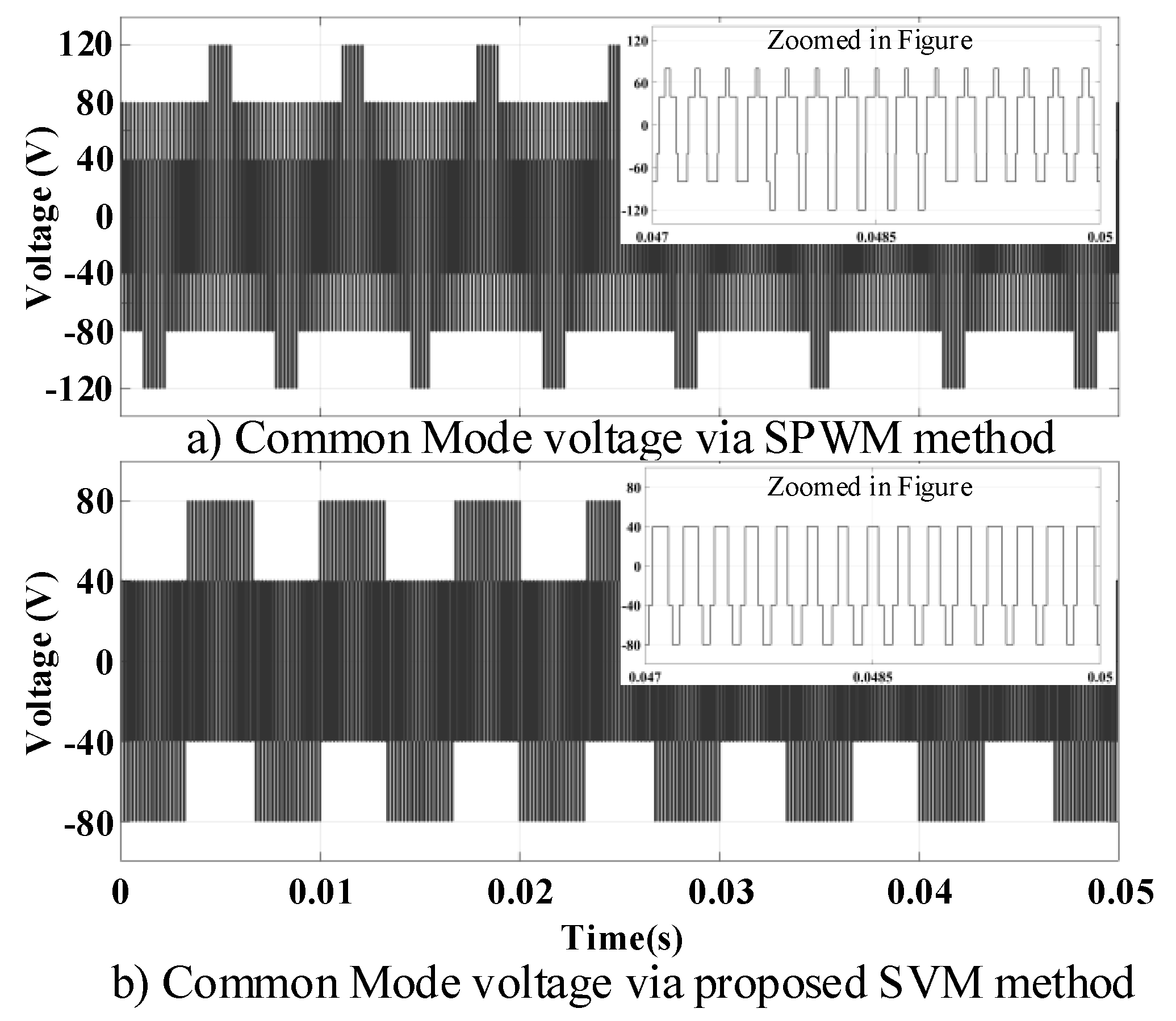
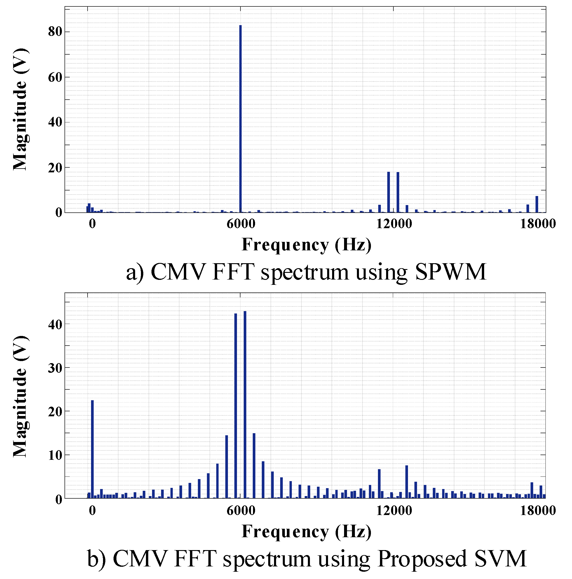
4. Simulation and Experimental Results

The simulation and experimental results of the proposed SVM method and modified SPWM are discussed in this section. This section consists of two parts: (1) simulation results and (2) experimental results. The power quality of the 10-switch inverter based on investigated modulation schemes are studied. The simulations for carrier-based modulation method are performed based on the modified version of prior methods applied for this inverter since this modified method has less computational calculations and yields the same result. Also, the experimental model is tested using the designed SVM method to validate the simulation results.

4.1. Simulation Results

Simulation of the 10-switch inverter based on SVM and SPWM methods is performed on Matlab Simulink 2017a. Table 6 shows the simulation system parameters related to the performed simulations.
Simulations are conducted under the same conditions to achieve a fair comparison between previously introduced SPWM and proposed SVM method on the 10-switch converter. Multiple factors are considered for evaluating the proposed modulation method. Since it is clear that SVM methods have 15.4% higher voltage utilization, all comparisons are made in a way that an equal output voltage and current will be achieved on the output of the converter. This means that in order to compare the results, the SVM modulation index is reduced by 15.4% to reach the identical peak values of voltage and current in simulation results. However, this modulation index reduction leads to higher THD in converter outputs.
Figure 9 shows system parameters of a 1.5 kW simulation system, in which three-phase balanced resistive loads are connected to the output of the inverter that is fed by two ideal constant DC voltage sources. Figure 8 shows the output line voltage of the converter obtained by SPWM and SVM methods, respectively. As it is seen from voltage waveforms of Figure 8, output voltage in the SPWM method has visible deformities, which cause an increase in THD value of output waveforms and the appearance of low order harmonics. Figure 9 shows that in both methods, the output voltage of the inverter owns a special three-level waveform which is exclusive to 2/3 hybrid converters.
The FFT spectrum and THD of the line voltage are studied in Figure 10. Results indicate that applying the proposed SVM method leads to an 11% THD reduction in line voltage of the converter in comparison to the SPWM method. Figure 10 demonstrates that in the carrier-based method, even harmonics with a value around 0.2% are present in the FFT spectrum, while in the proposed SVM even harmonics are eliminated, which results in improved outcomes. Investigating the third harmonic of the voltage via both modulation methods showed that the third harmonic of line voltage is omitted in the proposed SVM and the values of 5th, 7th, and 11th harmonics of voltage are decreased by 50% in the proposed modulation method. Also, low-order harmonics in the proposed SVM method have an insignificant value in comparison to the carrier based method. As the range of converter’s power application changes, the THD gap comparing two methods remains permanently. This significant THD decrease in the output voltage of the inverter shows the superiority of the designed SVM over prior SPWM methods. Moreover, comparing the output voltage value in Figure 9 leads to the conclusion that the two methods reached the fundamental component via different modulation indexes. This proves that the SVM method increases the DC voltage utilization by 15.4%.
Furthermore, the variation of the output voltage THD in terms of modulation index via two modulation methods is shown in Figure 11, which compares the results of applying two modulation methods. The chart proves that as the modulation index decreases, the output voltage THD gap between the two modulation methods grows rapidly and the converter outputs modulated by the proposed SVM shows superior performance at all modulation indexes. In the over modulation condition, the fundamental value of the output voltage is enhanced and the number of pulses in the line to line voltage waveform is reduced. The proposed method is advised to work under a normal condition since entering the over modulation condition requires application of the large vectors only, and the dwell time defined for the small vector has to be decreased gradually in the over modulation condition.
The common mode voltage of the inverter is investigated to reach investigate the converter from another aspect. CMV is defined as the voltage at the star point of the load and the system's ground. The magnitude of CMV is dependent on switching states and the grounding system. High CMV leads to various unwanted consequences such as undesired electromagnetic interference problems, insulation damage, and overvoltage stress on devices [18]. CMV of the 10-switch inverter is calculated by Equation (9), and it was measured in both SVM and SPWM simulations.
V c m = V a n + V b n + V c n 3
where V c m represents voltage between the middle point of the DC-link and neutral point of three-phase AC load. Comparison of the inverter’s CMV based on two method results is summarized in Figure 12, which shows that the CMV peak reduces from 120 V in SVM case to 80 V in SPWM. In other words, CMV drops from 50% of the total DC link to 33.33% when the modulation method is changed from SPWM to the proposed SVM. The RMS value of CMV is also measured and that once again indicates another advantage of the SVM method, as the rms CMV is decreased by 18.5% when the proposed SVM is used alternatively to the prior carrier-based method. The rms value of CMV using SPWM is 65 V, and it drops to 53 V when the proposed SVM method is used. Lower CMV level in the inverter leads to higher power quality, and also prevents extra heat dissipation on the inverter.
The CMV frequency spectrum using the two methods is depicted in Figure 13. The frequency spectrum of CMV indicates that the proposed SVM method has much more low-domain CMV in different switching frequencies in comparison to the SPWM method. The chart shows that CMV around the switching frequency is at its maximum level and when the SPWM method is used, the fundamental value of CMV is more than twice that of the SVM fundamental value. Thus, the SVM method that has lower peak CMV and lower RMS value becomes favorable. Multiple simulations are carried out to study the proposed SVM further and investigate its effect on the 10-switch converter’s operation. Figure 14 presents the THD variation of inverter’s output voltage in different switching frequencies. Once again, the modulation index for SVM cases is set 15.4% lower than SPWM simulations. THD chart shown in Figure 14 points out the advantage of the proposed SVM method over prior SPWM methods on the 10-switch inverter. AC line voltage THD shown in Figure 14 is almost identical in each modulation method at different switching frequencies. It is noted that the AC line voltage THD is reduced by 11% when the proposed SVM method is applied, and a constant gap exists between the THD levels of two modulation methods, that implies reaching high power quality when the proposed SVM is applied.
In order to achieve a specific fundamental output voltage via two mentioned modulation methods, different input power has to be injected to the converter. The total semiconductor power loss of the converter is dependent on the parameters of the semiconductor shown in Equation (10).
E o n = f 1 ( v , i c , T j ) E o f f = f 2 ( v , i c , T j ) V C E = f 3 ( i c , T j ) E r r = f 4 ( v , i c , T j ) V f = f 5 ( i c , T j )
where ic is the current that flows into the device, v is the voltage across the device, Tj represents the junction temperature, Eon the turn-on energy, Eoff the turn-off energy, Err the reverse recovery energy, Vce the saturation voltage (collector-emitter voltage), and Vf the on-state voltage of reverse recovery diode. The DC voltage utilization in the proposed SVM method has increased and therefore, more input power has to be injected to the converter using SPWM method to reach the same outputs, which means that the total power loss in SPWM case will increase. In order to compare the two methods, a constant certain output fundamental voltage is assumed. The proposed SVM method has a lower THD level in comparison to former SPWM methods, and it requires less input power to reach the assigned output value. This means the voltage across each semiconductor (v) will be lower in the proposed SVM method and as a result, power loss parameters (Eon, Eoff, Err, and Vf) are decreased since they are related to voltage across the device, junction temperature and the conducting current. Decreased power loss parameters leads to the reduction of the total power loss in the 10-switch converter.

4.2. Simulation in the Unbalanced AC Load Condition

The mid-point voltage DC-link is investigated to review the carrier-based and proposed SVM methods operation in the unbalanced AC load conditions. Table 7 shows the simulation system parameters of the unbalanced system. An unideal DC source is connected to two DC-link capacitors. Same simulation conditions are applied to both modulation methods. Figure 15 shows capacitor voltage of each DC-link pole. The proposed modulation completely controls the neutral point voltage and the results prove that the SVM method has acceptable converging mid-point voltage. However, the carrier-based method has higher voltage ripple, which requires balancing circuit to balance the DC-link pole voltages.

4.3. Experimental Results

The designed SVM is implemented on an experimental model of the 10-switch converter. DC sources are connected to the converter to feed the three-phase balance AC loads. In the experimental model, HGTG10N120BND is applied as a switch and HCPL3120 is used to work as a gate-driver and optocoupler simultaneously. The gate signals of converter switches are generated through the marked discovery board. In this model, STM32f407 is used as a microcontroller, which has a lower price rather than regular TI DSPs. This microcontroller is totally capable of processing the modulation method, since the computational steps of the modulation method is reduced via the proposed SVM method, and extra costs are prevented. The simulation results section showed the superiority of the proposed SVM method over the prior carrier-based modulation method from multiple points of view such as power quality, CMV, and DC-link voltage utilization. Hence, the presented SVM algorithm explained in Section 3 is fully implemented on the microcontroller to validate the simulation results. Full detailed model and types of applied equipment are listed in Table 8.
The three-phase AC loads are fed by two DC sources working as a bipolar dc side, and the results are shown in Figure 16 Phase and line voltages of the converter and CMV of the inverter are depicted in these figures. Experimental results of phase and line voltage of the inverter validate the three-level phase and line voltages depicted in the simulation results section. CMV of the experimented system demonstrated in Figure 17 proves that the peak CMV of the converter is reduced from 50% of the total DC-link to 33.3%, which is the same as simulation results.
The same procedure occurs for rms value of the converter’s CMV, which is decreased by about 25%. Based on the experimental data shown in Figure 16, the FFT spectrum of the AC phase and line voltages are analysed through MATLAB software, and the THD level of these signals were measured, which is represented in Figure 18. In simulation results, THD level of inverter AC output voltage in the same modulation index, time sample, and three-phase AC loads of the experimental model is about 59%, which points out that there is a negligible 3% difference between simulated model THD and its experimental one. The reason behind this difference is the assumption of ideal switching devices with low turn-on resistance, same turn-on and turn-off time of semiconductors and ideal equal loads in the simulations. Also, low order harmonics have appeared in the FFT spectrum of experimental results which is related to the assumption of ideal switching devices in simulation, the difference in rise and fall time of semiconductors in the experimental model of the system, and unequal loads in experimental tests.
The 10-switch converter is a bidirectional converter which is used as an inverter in this paper. This converter offers two DC voltage levels at the DC-side in rectifier mode. Unequal DC-loads connected to this converter result in transmitting unequal power flow from each pole of the DC-link, which creates an unbalanced condition in the neutral point of the dc-side and the DC-link voltage poles. A proper solution to this condition is applying an opposite small voltage vector in the switching pattern to rectify the unbalance Dc-load condition and balance the neutral point [19]. This idea is cost-effective and does not require any additional control methods or passive elements. Further studies on this idea are planned for future works.

5. Conclusions

This paper proposes a new SVM method for the new class of 2/3 level converters, called a 10-switch converter, with the ability to work under bidirectional power flow and various power ranges, plus it presents a bipolar dc side which offers flexible load connection options. The 10-switch converter using the new SVM method can be utilized in multiple power distribution applications. This SVM method is an alternative to previous SPWM methods. The prior SPWM methods are modified in this paper and compared to the proposed SVM method. Designed SVM has simplified switching algorithm which is superior to carrier-based modulation methods since it has a straightforward implementation and requires less computational effort. Main advantages of this novel SVM method include THD reduction of converter’s outputs along with a significant decrease in peak and rms CMV. Observing from the dc side point of view, applying the new SVM results in exploiting higher Dc link voltage as an inherent benefit of SVM. Simulation models and experimental results confirm reduced CMV and improved power quality of the proposed SVM method for the 10-switch converter.

Author Contributions

All authors contributed equally to this work and all authors have read and approved the final manuscript.

Funding

This research received no external funding.

Conflicts of Interest

The authors declare no conflict of interest.

References

  1. Jagabar, J.S.; Krishnaswamy, V. An assessment of recent multilevel inverter topologies with reduced power electronics components for renewable applications. Renew. Sustain. Energy Rev. 2018, 82, 3379–3399. [Google Scholar]
  2. Siwakoti, Y.P.; Peng, F.Z.; Blaabjerg, F.; Loh, P.C.; Town, G.E. Impedance-source networks for electric power conversion Part I: A topological review. IEEE Trans. Power Electron. 2015, 30, 699–716. [Google Scholar] [CrossRef]
  3. Strasser, T.; Member, S.; Andrén, F.; Kathan, J.; Cecati, C.; Buccella, C.; Member, S.; Siano, P.; Member, S.; Leitão, P.; et al. A Review of Architectures and Concepts for Intelligence in Future Electric Energy Systems. IEEE Trans. Ind. Electron. 2015, 62, 2424–2438. [Google Scholar] [CrossRef] [Green Version]
  4. Dragičević, T.; Lu, X.; Vasquez, J.C.; Guerrero, J.M. DC Microgrids—Part II: A Review of Power Architectures, Applications, and Standardization Issues. IEEE Trans. Power Electron. 2016, 31, 3528–3549. [Google Scholar] [CrossRef] [Green Version]
  5. Hasan, N.S.; Rosmin, N.; Osman, D.A.A.; Musta’amal@Jamal, A.H. Reviews on multilevel converter and modulation techniques. Renew. Sustain. Energy Rev. 2017, 80, 163–174. [Google Scholar] [CrossRef]
  6. Schweizer, M.; Friedli, T.; Kolar, J.W. Comparative evaluation of advanced three-phase three-level inverter/converter topologies against two-level systems. IEEE Trans. Ind. Electron. 2013, 60, 5515–5527. [Google Scholar] [CrossRef]
  7. Rodriguez, J.; Bernet, S.; Steimer, P.K.; Lizama, I.E. A survey on neutral-point-clamped inverters. IEEE Trans. Ind. Electron. 2010, 57, 2219–2230. [Google Scholar] [CrossRef]
  8. Gupta, K.K.; Ranjan, A.; Bhatnagar, P.; Sahu, L.K.; Jain, S. Multilevel inverter topologies with reduced device count: A review. IEEE Trans. Power Electron. 2016, 31, 135–151. [Google Scholar] [CrossRef]
  9. Schweizer, M.; Kolar, J.W. Design and implementation of a highly efficient three-level T-type converter for low-voltage applications. IEEE Trans. Power Electron. 2013, 28, 899–907. [Google Scholar] [CrossRef]
  10. Mihalache, L. A hybrid 2/3 level converter with minimum switch count. In Proceedings of the 2006 IEEE Industry Applications Conference Forty-First IAS Annual Meeting, Tampa, FL, USA, 8–12 October 2006; Volume 2, pp. 611–618. [Google Scholar]
  11. Sharifzadeh, M.; Vahedi, H.; Sheikholeslami, A.; Labbé, P.A.; Al-Haddad, K. Hybrid SHM-SHE Modulation Technique for a Four-Leg NPC Inverter With DC Capacitor Self-Voltage Balancing. IEEE Trans. Ind. Electron. 2015, 62, 4890–4899. [Google Scholar] [CrossRef]
  12. Muniz, J.H.G.; Da Silva, E.R.C.; Da Nobrega, R.B.; Dos Santos, E.C. An improved pulse-width-modulation for the modified hybrid 2/3-level converter. In Proceedings of the 2013 Brazilian Power Electronics Conference, Gramado, Brazil, 27–31 October 2013; pp. 248–253. [Google Scholar]
  13. Wu, B.; Narimani, M. High-power Converters and AC Drives; John Wiley & Sons: Hoboken, NJ, USA, 2017; Volume 59, ISBN 1119156033. [Google Scholar]
  14. Narendrababu, A.; Agarwal, P. Virtual Vector Modulated Hybrid 2/3-Level Z-source VSI for PV Applications. In Proceedings of the 2018 9th IEEE International Symposium on Power Electronics for Distributed Generation Systems (PEDG), Charlotte, NC, USA, 25–28 June 2018; pp. 1–7. [Google Scholar]
  15. Rahimi, R.; Moradi, G.R.; Afshari, E.; Farhangi, B.; Farhangi, S. Study of Leakage Current Phenomena in Hybrid 2/3-Level Three-Phase Transformerless Photovoltaic Grid-Connected Inverters. In Proceedings of the 1st International Conference on New Research Achievements in Electrical and Computer Engineering (ICNRAECE), Tehran, Iran, 13 May 2016. [Google Scholar]
  16. Teichmann, R.; Bernet, S. A Comparison of Three-Level Converters Versus Two-Level Converters for Low-Voltage Drives, Traction, and Utility Applications. IEEE Trans. Ind. Appl. 2005, 41, 855–865. [Google Scholar] [CrossRef]
  17. Zhou, K.; Wang, D. Relationship between space-vector modulation and three-phase carrier-based PWM: A comprehensive analysis. IEEE Trans. Ind. Electron. 2002, 49, 186–196. [Google Scholar] [CrossRef]
  18. Hava, A.M.; Ün, E. Performance analysis of reduced common-mode voltage PWM methods and comparison with standard PWM methods for three-phase voltage-source inverters. IEEE Trans. Power Electron. 2009, 24, 241–252. [Google Scholar] [CrossRef]
  19. Najafi, P.; Hooshmand Viki, A.; Shahparasti, M. Novel space vector-based control scheme with DC-link voltage balancing capability for 10-switch converter in bipolar hybrid microgrid. Sustain. Energy Grids Netw. 2019, 20, 100256. [Google Scholar] [CrossRef]
Figure 1. Schematic of a 10-switch inverter.
Energies 13 01855 g001
Figure 2. Sinusoidal pulse width modulation (SPWM) flowchart of a 10-switch converter.
Energies 13 01855 g002
Figure 3. Space vector diagram of the 10-switch converter.
Energies 13 01855 g003
Figure 4. Region determination of each sector.
Energies 13 01855 g004
Figure 5. Projection of normalized reference voltage vector.
Energies 13 01855 g005
Figure 6. Vector and dwell time combination in sector I.
Energies 13 01855 g006
Figure 7. Seven-segment switching sequence in region 2 of sector I.
Energies 13 01855 g007
Figure 8. Designed space vector modulation (SVM) calculation flowchart.
Energies 13 01855 g008
Figure 9. Converter’s output line voltage using SPWM and proposed SVM method.
Energies 13 01855 g009
Figure 10. FFT spectrum of the converter’s output line voltage.
Energies 13 01855 g010
Figure 11. Total harmonic distortion (THD) curve of the output voltage of the inverter in terms of the modulation index.
Energies 13 01855 g011
Figure 12. Common mode voltage (CMV) comparison in the SVM and SPWM methods.
Energies 13 01855 g012
Figure 13. Common Mode Voltage frequency spectrum using two modulation methods.
Energies 13 01855 g013
Figure 14. Line voltage THD in different switching frequencies comparing the proposed SVM and SPWM.
Energies 13 01855 g014
Figure 15. DC-link voltages of each pole in unbalanced AC load condition using two methods.
Energies 13 01855 g015
Figure 16. Phase and line voltages of AC loads connected to the 10-switch converter.
Energies 13 01855 g016
Figure 17. CMV of the experimental model of the 10-switch converter modulated by proposed SVM.
Energies 13 01855 g017
Figure 18. Experimented converter’s output phase and line voltages FFT spectrum at modulation index = 0.8.
Energies 13 01855 g018
Table 1. Switching states of the 10-switch converter and their representation.
Switching StateON SwitchesTerminal Voltage
PS1AS1 or S3 or S5E ( V d c 2 )
OS2AS1 or S3 or S50
S3AS2 or S4 or S6
NS4AS2 or S4 or S6−E ( V d c 2 )
Table 2. Ten-switch converter space vector table.
Vector ClassificationSpace VectorSwitching StateVector Magnitude
Zero VectorV0PPP
OOO
NNN
0
Small Vector (V1 to V6) P-TypeN-Type V d 3
V1PPOO
V1N ONN
Large Vector (V7 to V12)V7PNN 2 V d 3
Table 3. Region determination based on normalized reference voltage vector.
CaseAngle (θ)Region
M 1 0.5 & M 2 0.5 & M 1 + M 2 0.5 NA1
M 1 > 0.5 or M 2 > 0.5 or M 1 + M 2 > 0.5 θ 30 2
θ > 30 3
Table 4. Dwell times of voltage vectors in the sector I.
Dwell Time RegionTaTbTc
1 V 1 2 3 V r e f T s V d c sin ( π 3 θ ) V 2 2 3 V r e f T s V d c sin ( θ ) V 0 T s 2 3 V r e f T s V d c sin ( π 3 + θ )
2 V 1 2 T s V r e f T s V d c ( 3 cos θ + 3 sin θ ) V 7 3 V r e f T s V d c ( cos θ ) T s V 8 3 V r e f T s V d c ( sin θ )
3 V 2 2 T s 3 V r e f T s V d c ( 3 cos θ + sin θ ) V 7 3 V r e f T s 2 V d c ( 3 cos θ sin θ ) V 8 3 ( 9 T s V r e f sin θ 2 3 T s V d c + 3 3 T s V r e f cos θ ) 6 V d c
Table 5. Switching sequence transition comparison between SPWM and proposed SVM methods.
Segments of Switching Sequence in Carrier-Based Modulation at the Three Intervals of Sector I.
Interval 1ONNPNNPPNPPPPPNPNNONN
Interval 2ONNPNNPPNPPOPPNPNNONN
Interval 3NNNPNNPPNPPOPPNPNNNNN
Segments of Switching Sequence in the Proposed SVM in Regions 2 and 3 of Sector I.
Region 2ONNPNNPPNPOOPPNPNNONN
Region 3PPOPPNPNNOONPNNPPNPPO
Table 6. Simulation system parameters.
System ParameterValue
Switching Frequency6 kHz
Total DC-link Voltage240 V
System Frequency50 Hz
Three-phase AC Load1.5 kW
11.506 Ω
Sampling Time2 µs
Modulation Index0.78 (SVM)
0.9 (SPWM)
Table 7. Simulation system parameters in unbalanced three-phase AC load condition.
Unbalanced Simulation ParametersParameter Values
Three-Phase AC LoadPhase A
R = 11.506 Ω
L = 5 mH
Phase B
R = 3 Ω
L = 5mh
Phase C
R = 11.506 Ω
L = 5 mH
Dc-link CapacitorsC1 = 220 µF
C2 = 220 µF
DC Source Voltage240 V
Internal Resistance of DC sourceR = 0.01 Ω
Table 8. System parameters of experimental model.
System ParameterValue
IGBT Model NumberHGTG10N120BND
Gate Drive OptocouplerHCPL-3120
Switching Frequency6 kHz
Total DC-link Voltage60 V
System Frequency50 Hz
Three phase AC Load56 Ω
Timer Clock12 MHz

