Article

Deployment of a Bidirectional MW-Level Electric-Vehicle Extreme Fast Charging Station Enabled by High-Voltage SiC and Intelligent Control

Department of Electrical Engineering and Computer Science, University of Tennessee, Knoxville, TN 37996, USA
*
Author to whom correspondence should be addressed.
Energies 2020, 13(7), 1840; https://doi.org/10.3390/en13071840
Submission received: 24 March 2020 / Revised: 5 April 2020 / Accepted: 7 April 2020 / Published: 10 April 2020
(This article belongs to the Special Issue Intelligent Transportation Systems for Electric Vehicles)

Abstract

:
Considering the fact that electric vehicle battery charging based on the current charging station is time-consuming, the charging technology needs to improve in order to increase charging speed, which could reduce range anxiety and benefit the user experience of electric vehicle (EV). For this reason, a 1 MW battery charging station is presented in this paper to eliminate the drawbacks of utilizing the normal 480 VAC as the system input to supply the 1 MW power, such as the low power density caused by the large volume of the 60 Hz transformer and the low efficiency caused by the high current. The proposed system utilizes the grid input of single-phase 8 kVAC and is capable of charging two electric vehicles with 500 kW each, at the same time. Therefore, this paper details how high-voltage SiC power modules are the key enabler technology, as well as the selection of a resonant-type input-series, output-parallel circuitry candidate to secure high power density and efficiency, while intelligently dealing with the transient processes, e.g., pre-charging process and power balancing among modules, and considering the impact on the grid, are both of importance.

1. Technical Challenges of EV Extreme Fast Charging Stations

Transportation is revolutionizing as the world welcomes the benefits of electric transportation. The growing interest in electric vehicle (EV) technology is due to their minimum fuel emissions and air pollution. The demand for this kind of vehicles is growing, and the rate of this growth is also expected to increase in the forthcoming years [1,2]. However, there are concerns to be addressed in this regard, including time of charge, range anxiety, cost of charging, and negative impact of charging demand on the grid. Range anxiety and time of charge are the issues that have been addressed in recent years through developing EV fast chargers. Sixteen hours are needed for level-1 chargers, while only 10 minutes are needed for extreme fast chargers (XFCs). This by itself shows how the charging process can impact the adoption of plug-in hybrid electric vehicles. The concept of a gas-station-like experience for charging EVs has become a reality in recent years due to the advancement of XFCs [3,4], e.g., chargers rated at 400 kW and above. The focus of this work is to design a 1 MW XFC station for two EVs, i.e., 500 kW per car. Take Tesla Model S as an example, which has 75 kWh battery pack. If the state-of-charge (SOC) window is 80%, a 500 kW XFC is then able to charge an EV within 75 kWh × 80%/500 kW = 7 m, presuming the charging loss is ignorable.
While the majority of EV fast charging stations in the United States have a grid connection of three-phase 480 VAC, which is rectified into a DC bus (normally between 600 VDC and 800 VDC), followed by a DC/DC converter with galvanic isolation. Using such an approach to provide 1 MW sees a challenge from high grid current, which in turn challenges the 480 VAC transformer design. As shown in Table 1, the traditional 500 kVA XFC uses a grid transformer of more than 5000 L and more than 2000 kg. To enhance the system power density and reduce cost, elimination of such bulky and heavy grid transformers is a must [5].
Recently, wide-bandgap (WBG) semiconductor devices have played a role in developing EV chargers [6,7], not only increasing the power density thanks to the higher switching frequency than Si, but also undertaking higher input voltage, such as 6.5 kV silicon carbide (SiC). This potentially allows the medium voltage (MV) transmission lines (2.4–13.4 kVAC) directly to come into the charging station, thereby saving the 480 VAC step-down grid transformers. As compared in Table 1, elimination of the grid transformer can significantly reduce the size and weight of the overall XFC system. Even though the DC/DC converter such as dual active bridge (DAB) and resonant circuits (LLC and CLLC) all need transformers [8,9,10], such transformers can be operated at a much higher switching frequency, thereby seeing less weight and size penalty while maintaining galvanic isolation.
From Table 1, we can find that the overall efficiency of the proposed 500 kVA system based on the HV SiC switches is improved by 3%. The main reasons for the higher efficiency of the proposed system are as follows. 1) The normal input grid voltage of the traditional 500 kVA system is three-phase 480 VAC, and the input grid voltage of the proposed 500 kVA system is single-phase 8 kVAC, which is more than 17 times that of the traditional system. Given the same power level, higher voltage means lower current, which is beneficial to reduce the power loss of the whole transmission and improve system efficiency. 2) Enabled by 6.5 kV high voltage SiC power modules, the proposed system will connect to MV transmission lines (2.4–13.4 kVAC), thereby directly saving the 480 VAC step-down grid transformers. Therefore, the large power loss of the 60 Hz transformer is eliminated, which helps to achieve the higher efficiency. Additionally, a bidirectional feature is highly demanded, especially when there is a grid outage.
With the above consideration and enabled by high voltage (HV) SiC power modules, an approach shown in Figure 1 is proposed. The input 8 kVAC was split evenly among three H-bridge modules, which act as the power factor controller. The AC is then rectified into 4.3 kVDC, which is forwarded to a resonant-type DC transformer circuit (DCX) made of a primary half-bridge, a three-winding transformer, and two low-voltage H-bridge paralleled to output 1.3 kVDC. Note that this allows the two low-voltage DC (LVDC) buses to be isolated, thereby charging two cars in an isolated manner. The outputs of each of the DCX modules are connected in a parallel output to generate 1 MW power. Each LVDC bus then is connected to a 500 kW buck converter to charge one EV, as shown in Figure 1b.
Essentially, such an input-series, output-parallel (ISOP) design successfully eliminates the 480 VAC/60 Hz transformer, while it also realizes bidirectional power flow. Such an ISOP system, however, brings other challenges. 1) Device electrical ratings. With 8 kVAC single-phase grid, the grid connection of each power factor correction (PFC) module is desired to be at 2.6 kVAC, which is further boosted to 4.3 kVDC. For a 1 MW charging capability, each DC/DC converter module undertakes 333 kW. Selecting the right topology to minimize electrical stress of the switches is key to the success, especially for the DC/DC stage. A detailed comparison of various DC/DC topologies is shown in Table 2, including DAB, DCX, and CLLC. These topologies were chosen because they all provide isolated bidirectional DC/DC conversion by means of a high-frequency transformer and are all widely used [8,9,10,11,12]. As seen in Table 2, even though the peak current and root mean square( RMS) current are high with the DCX converter, the maximum switching off current is close to 0. This is because the DCX topology always operates at the resonant frequency, which is the main reason this paper selects such topology. All SiC devices are switched at 30 kHz in all compared topologies.
The electric stress is then shifted to the resonant circuit and MV transformer. The PFC stage also needs to realize unity power factor and reduce total harmonic distortion (THD), and given the input series structure of the PFCs, the interleaved gate signal is supplied to the PFCs to achieve much smaller current ripple, which could help to reduce the demand of the large bulky DC bus capacitor. This is of importance when reducing the dimensions and cost of the system and improving the power density of the system. Besides, the smart output voltage balancing control is proposed to make sure the three PFC modules have balanced output voltage even under the different load conditions. The balanced output could ensure the same voltage stress among different modules, which is beneficial to the safe operation of the system. This part will be discussed further in Section 2. The DCX topology steps down 4.3 kVDC to a level of ~1.3 kVDC. Considering the importance of the resonance of the DCX, the intelligent resonant frequency tracking method based on the master–slave control is proposed. This control method could adjust the working frequency automatically to reach the resonant frequency, and the master-slave control enables the automatic change of the frequency adjustment operand. Considering that the resonant condition is necessary for the low switching loss of the switches, this novel control method is indispensable for the high-efficiency and safe operation of the system. Given the high-power level and high-voltage level, to avoid the inrush current at the start of the system, the DCX is responsible for pre-charging the output capacitor of the LVDC buses before charging. These control methods will be detailed in Section 3. Section 4 will discuss the impact on the grid. Section 5 is the conclusion.

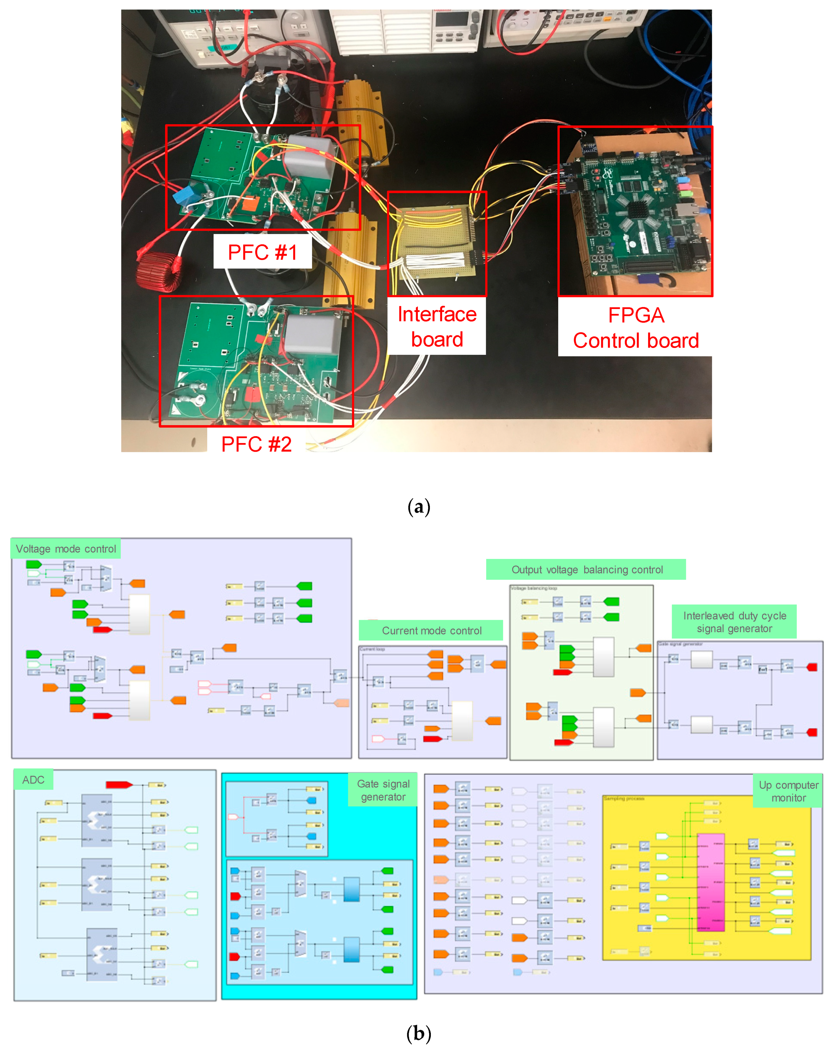
2. PFC-Stage Control

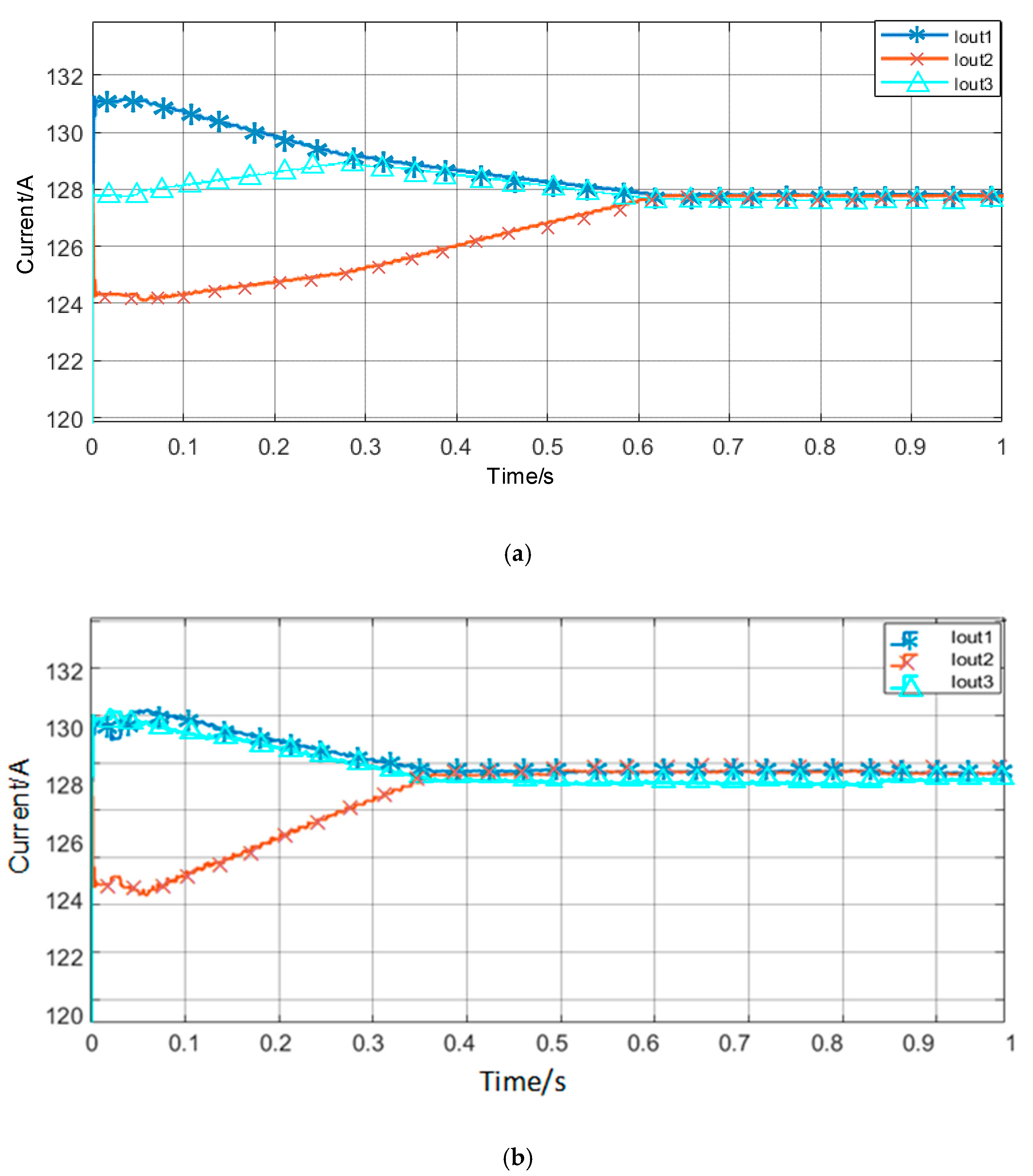
2.1. Power Balancing

Since the basic control method of the totem-pole PFC has been widely discussed [13,14], this paper will particularly focus on the power balancing among modules. To simplify the analysis, just consider two series PFC stages as shown in Figure 2.
To rectify the AC power from the power grid, the bridge leg of the PFC #n {Sn3, Sn4} is operated with main power frequency, i.e., 50/60 Hz, which could be seen as the rectifier bridge leg. Another bridge leg of the PFC #n {Sn1, Sn2} is pulse width modulation (PWM) controlled to achieve the power factor correction and low THD. In the steady state of this system, because the voltage and current are in phase, the DCX could be considered as the resistive load. Because the switching frequency fs is much higher than the line frequency fg, vin(t) can be assumed as constant within one switching period. Considering the continuous conduction mode (CCM) for both PFCs, steady-state equations can be derived as follows [15]:
V o 1 ( 1 d 1 ) + V o 2 ( 1 d 2 ) = | V i n |
V o 1 = | i i n | ( 1 d 1 ) R 1
V o 2 = | i i n | ( 1 d 2 ) R 2
where d1 and d2 represent the duty cycle of the high-frequency gate signals of PFC#1 and PFC#2.
From Equations (2) and (3), it can be seen that to achieve the output voltage balancing control under the unequal load condition, the duty cycles of two PFCs need to be modulated to accommodate the load difference [15,16]. Figure 3 shows the control block of the PFC weighted output voltage balancing control, composed of three loops, i.e., inner current control loop, outer voltage control loop, and the supplementary voltage balancing loop. The slower outer voltage control loop is to make the PFC stage output voltage follow the reference voltage and supply the reference current to the inner current control loop. The reference current is generated by the averaged voltage loop output Vvoa and the grid side voltage Vin, where Vvoa supplies the magnitude and vin with its RMS value Vin provides the phase of the reference current.
The impact of the load difference is thereby eliminated through the voltage balancing control loop, as simulated in Figure 4a,b, where the load of each PFC is not identical, R2 = 1.1R1. Without balancing control, some diversity of the switch can cause the DC-bus variation. Based on Equations (2) and (3), the same duty cycle will be supplied to two PFCs. Because of the series input structure, the input current will be the same for two PFCs. Therefore, the different load resistance will cause the unbalanced output. The simulation results of the steady-state output voltage waveform without the balancing control is shown in Figure 4a. When the voltage balancing loop is integrated into the control loop, two PFCs can be controlled individually. Voltage balancing loop could compensate for the deviation of the duty cycle caused by the different loads. After the compensation, the different duty cycle generated based on the output voltages of two PFCs will be supplied to the corresponding PFCs, such that the balanced output could be achieved. Figure 4b shows the voltage balancing control performance based on the simulation model. We then further experimentally validated the voltage balancing control for PFC stages, where we consider the load resistances of two PFCs to be 2R1 = R2 = 25 Ω. The experimental setup and the Field Programmable Gata Array (FPGA) control block diagram is shown in Figure 5, and the experimental results are shown in Figure 6. Figure 6a shows the steady-state input and output waveform without the balancing control. It can be seen that the output DC voltage of PFC#1 is almost twice of the output DC voltage of PFC#2. Considering that the load R2 is twice of the load R1, the experimental results are consistent with the theoretical analysis. As shown in Figure 6b,c, after integrating the voltage balancing control, the DC bus voltages are kept the same once the system reaches steady state. Therefore, the voltage balancing control method is validated by the simulation and experiments.

2.2. Interleaving Control

Once the three PFC modules balance the power in the modules, we can further employ interleaving control for each PFC, i.e., shifting the gate signals by 120° (1/3Ts). This helps further reduce the grid-side current. As shown in Figure 7a, without the interleaving, the grid side current (I_inductor) sees over 20 A current ripple. With the interleaving control, as shown in Figure 7b, the grid current ripple drops to ~5 A.

3. DCX Stage Control

3.1. Power Balancing Control

The DCX converter topology, as seen in Figure 1a, consists of a MOSFET half-bridge converter on the primary side, a three-winding MV transformer, a resonant capacitor and a MOSFET full-bridge converter on each secondary side. The primary-side and secondary-side MOSFETs share the same complementary PWM gate signals with 50% duty cycle. The relationship of the resonant frequency fr and the resonant parameters can be expressed by Equation (4), where Lr is the leakage inductance of the transformer and Cr represents the capacitance of the resonant capacitor.
2 π f r = 1 L r C r
As previously mentioned, the PFC stage could achieve balanced output voltage, which means that each of the DCX converters will have the same input voltage. However, a slight difference between transformers leakage inductance or the resonant capacitance will lead the converter to deviate away from the resonance point and further creates an unbalanced output current. The main challenge of this unbalanced problem is that when the switching frequency is higher or lower than the actual resonant frequency of the DCX, they both can cause the output current to decrease and unbalance the outputs. Thus, we need to detect the impedance of the resonant tank to determine the changing direction of the switching frequency. To solve this problem intelligently and easily, output current balancing control based on the resonant frequency control is proposed in this paper and shown in Figure 8.
It is noticeable that when the switching frequency of one DCX converter in this paralleled structure is closer to its resonant frequency, its output current will be larger. Thus, in this control method, the DCX converter which has the highest output current will be set as the master converter, and other DCX converters will automatically become the slaves. The frequency of the master will be constant, and the frequency of the slave will be adjusted to match the resonant frequency of the DCX converter. The resonant frequency tracking control is mainly controlling the changing direction of switching frequency based on the changing of the output current. The time step ts and frequency step ∆f are constant and can be adjusted according to the system parameters and requirements of the control accuracy. Then, if the output current of DCX #n increased after the last change of the frequency (when time t = (k − 1)ts), the changing direction of the frequency will stay the same as the last time (when time t = kts). Conversely, the frequency will change in the opposite direction. The control goal is to track the resonant frequency of each DCX automatically and achieve the balanced output currents.
Compared with the control method based on phase relationship detection [17] and time measurement of zero diode current [18], among others, the proposed method has three main advantages: 1) changing fs bi-directionally and automatically tracking the resonant condition; 2) setting the master automatically to make all the DCX converters work under the resonant conditions when the system is at the steady state; and 3) having no extra detection and measurement circuit.
Based on three paralleled DCXs, the simulation is conducted to validate the output current balancing control. Three DCXs have different resonant inductors but have the same initial working frequency finitial:
f i n i t i a l = 1 2 π L r d C r d = 20 kHz
where Lrd and Crd represents the designed resonant inductance and capacitance.
Figure 9a,b shows the output current balancing process of three parallel-connected outputs under two sets of different initial parameters of inductors, 1) Lr1 = Lrd, Lr2 = 0.9 Lrd, Lr3 = 0.95 Lrd and 2) Lr1= 1.05 Lrd, Lr2 = 0.9 Lrd, Lr3 = 0.95 Lrd. For the first set, based on the control algorithm, there are mainly three stages for the balancing process. First, when t < 0.02 s, the system works without the balancing control, and the output currents are unbalanced, which is caused by the different resonant condition. From Figure 9a, when t < 0.02 s, it can be seen that the DCX#1 with the best resonant condition has the largest output current, which is consistent with the theoretical analysis that a better resonant condition will lead to larger output current. Then, when t > 0.02 s and before the system reaches the balanced condition (where the deviation of currents are less than 0.3 A), the first DCX is the master controller as it has the largest current and the other two DCXs become the slave automatically. The frequency of the master converter will keep consistent, and two slaves will adjust the frequency to reach the resonant frequency based on the algorithm. Finally, when the output currents reach balance, the algorithm will automatically stop changing the frequency and keep the system working under this steady-state condition. Similar to the first set, the modulation process of the second set also has three modulation stages, which are shown in Figure 9b. The difference is that, for the second set, DCX#1 and DCX#3 have similar frequency deviation, so at first, the output current of these two DCXs are close to each other.
Figure 10 shows the voltage and current waveforms of the transformer primary sides of DCX#2 before and after the DCX reaches the resonant condition. After the DCX reaches the resonant condition, the transformer current waveform changes to a sinusoidal waveform, and the current and voltage are exactly in phase, which indicates zero-current switching-on and -off loss. Figure 11 shows the frequency modulation process of DCX#2 and DCX#3 when the system works under the first set of the parameters of inductance shown in Figure 9a. From Figure 11, we can find that first, the DCX#2 and DCX#3 could modulate the frequency to the real resonant frequency, which is determined by the inductor and capacitor, based on the deviation of the resonant frequency; and second, when the system reaches the resonant condition, the frequency modulation will stop and the controller will keep the frequency constant, such that three DCXs will work on the steady state with balanced outputs.

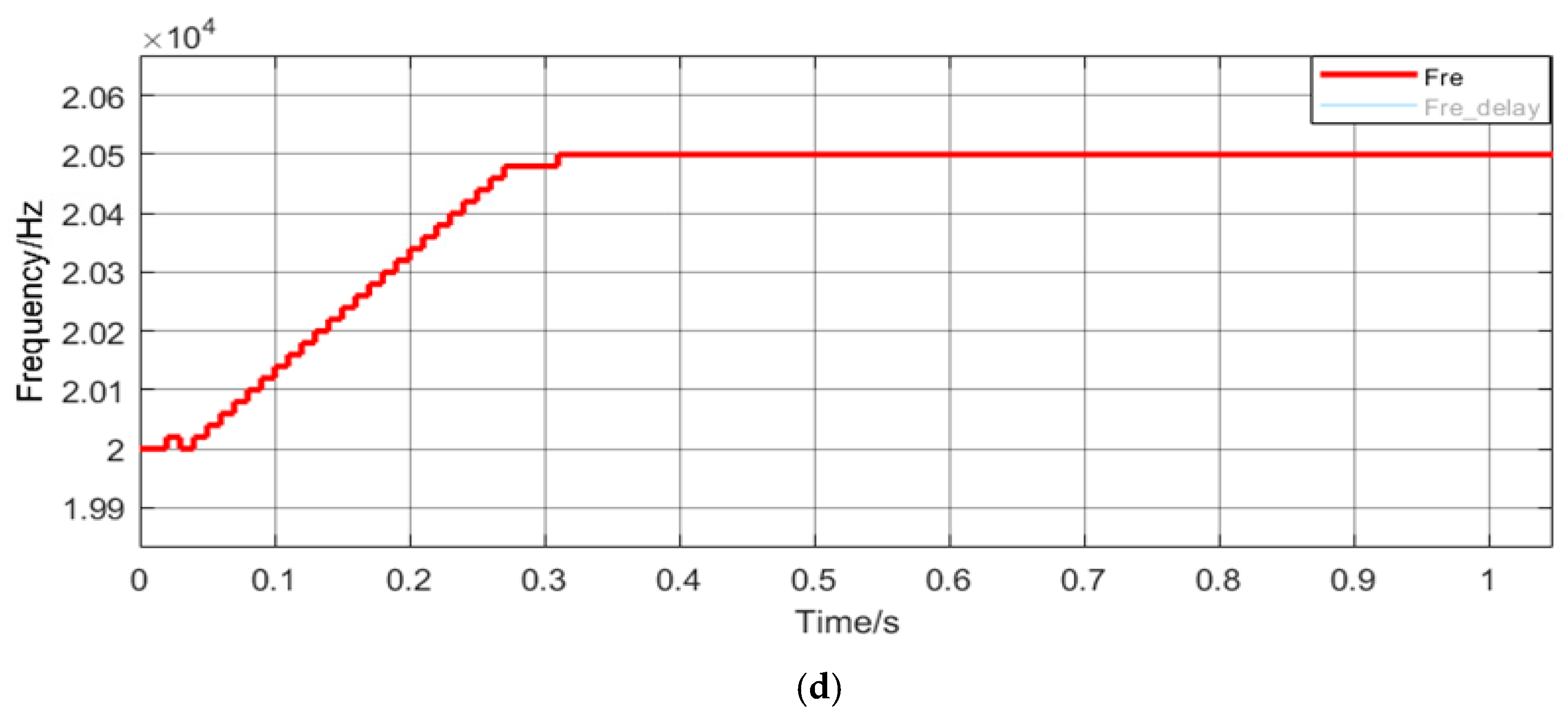
3.2. Pre-Charging Process

Considering high power and voltage level, we need to pre-charge the output capacitor of the LVDC bus before starting to charge the vehicle. Given the nature of its voltage source, directly providing 50% duty cycle for all switches will induce the large inrush current [19]. Instead, we propose to use a smaller duty cycle for the primary-side switch of the DCX in the starting process and prolong the charging time. The simulation results of pre-charging control are shown in Figure 12. Figure 12a shows the pre-charging process; meanwhile, Figure 12b shows the duty cycle of the gate signal changing process. When the system works at steady state, for DCX, the gate signals for the primary and secondary side switches are exactly in phase and with duty cycle of 50%. Differently from the steady state, when the system works on pre-charging stage, the duty cycle of the primary side will increase gradually from 0% to 50%. In this way, we can make sure that the charging power is small at first, which could decrease the dv/dt and charging current of the DC bus capacitor. Figure 12c shows the waveform of the current and voltage during the pre-charging process. From Figure 12c, we can find that the duty cycle smaller than 50% could decrease the current flowing to the capacitor, which is achieved by smaller conduction time. Figure 12d shows the relationship of the pre-charging time and peak value of the current flowing through the primary side switches. The peak current can be seen decreasing as the pre-charging time is increased, which could help to choose the appropriate pre-charging time based on the current rating of devices.

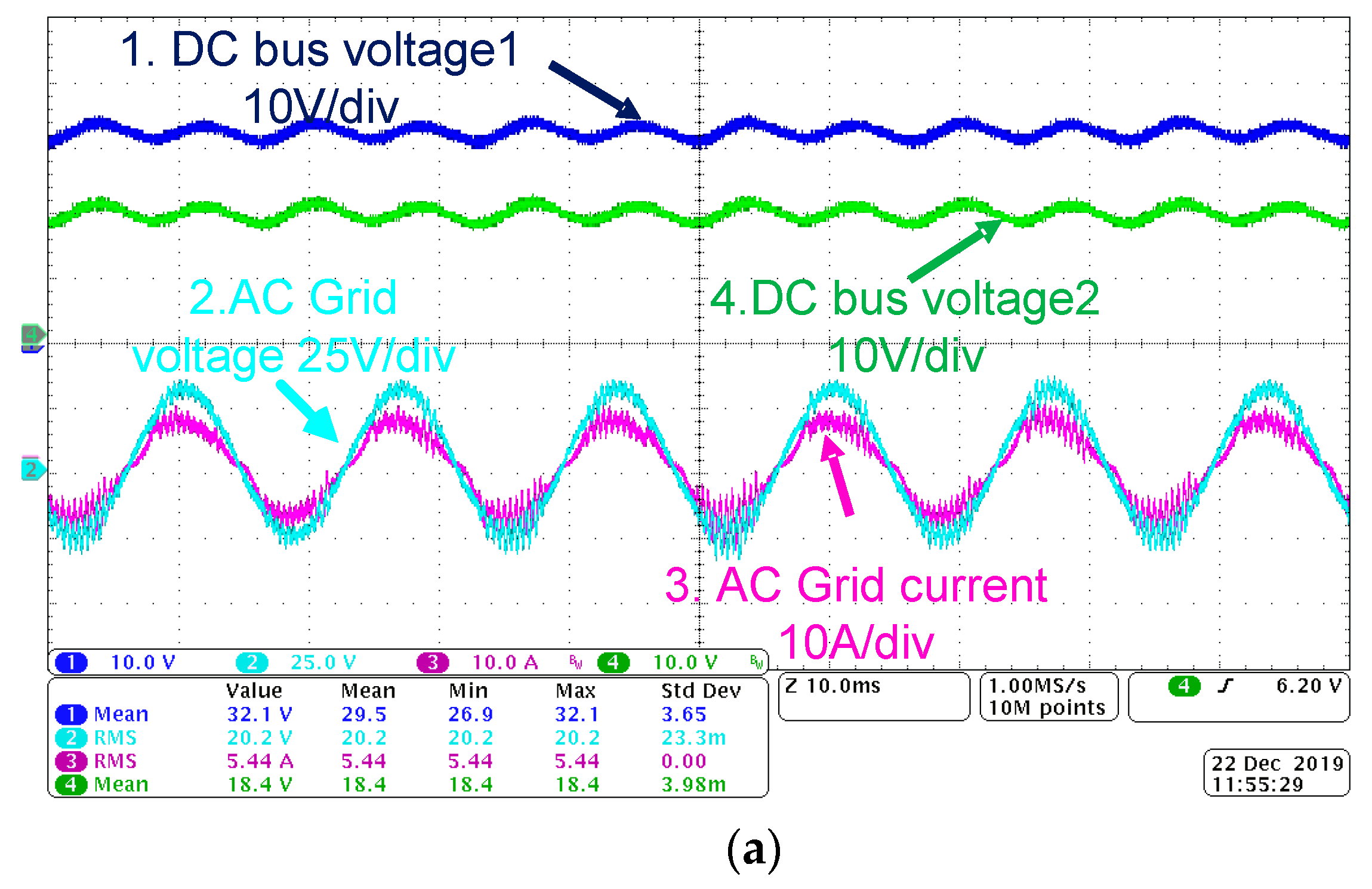
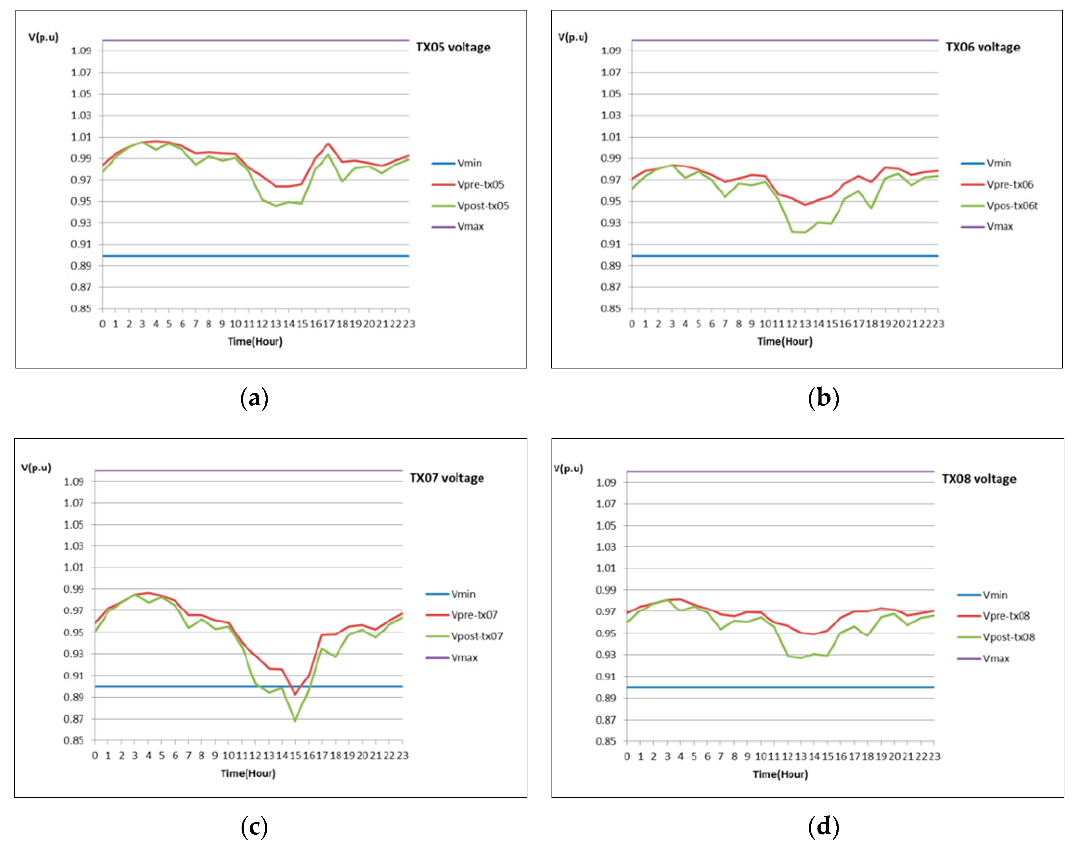
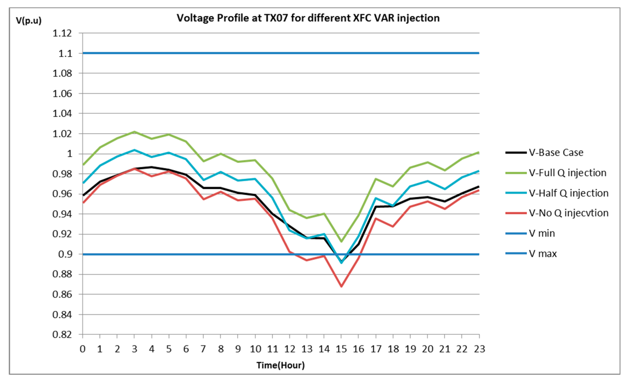
4. Interaction with the Grid

How to fit such a charger to the grid is another concern of this study. In this study, we are using a quasi-steady-state approach with a one-hour resolution to study the effect of installing XFCs on the feeders. For this purpose, the highest load day in 2019 has been picked and the one-hour snapshots of the grid have been selected as the base cases. The snapshots are basically real-time models of the network generated from the real energy management system (EMS) data by state estimators. Topology changes, load variations, generation units’ dispatch, and all other grid specifications that are subject to change are included in these models. These snapshots are being generated every ten minutes, but since the demand model for the XFC demand has a one-hour resolution, the snapshots are chosen accordingly. The models are real models of “Utility D”.
The XFC demand model that has been chosen for this study is the model that has been suggested in [20]. Authors suggested this demand model based on field data surveys and used statistical methods to generate a MW/time model for the demand for a week, which is shown in Figure 13. What we are using is an hourly demand model for a day which has the highest value during the week.
In our study, to have a more realistic sense of the effect of chargers on the higher-level grid, we have considered 20% of maximum loadability of the Transmission/Distribution transformer as the aggregated nominal charging power of the stations which are installed at the feeder. The MW demand associated with the time of the day is being added to a certain predetermined substation in the corresponding snapshot. For example, MW demand for 23:00 is added to the substation in the 23:00 snapshot. For each location, it is done for 24 h of a day. Then, the voltage variation, voltage violation, and transformer rating violation are monitored during the day. The results are further investigated for the aforementioned penetration of the EV chargers in the selected locations.
The first step for implementing the study was to choose the substations and geographic areas which make sense in the real world to install XFC stations. Through the field research from operational planning engineers in “Utility D”, five different areas with 19 transformers in total have been selected as candidates for the study. These areas are mostly airport, commercial, residential, or touristic areas in the state. All the locations in one area are studied together so that we can have a good understanding of how moving the XFC station might affect the grid locally. In all cases, the power factor has been considered. Therefore, the station is not absorbing any reactive power from the network.
To explain the research findings compactly, only the simulation results of four feeders in Area 2 are shown in Figure 14. Other areas have similar results with Area 2. Area 2 is mostly an important business area with four feeders as the options for connecting the XFC stations. From Figure 14a,b,d, we can find that tx-05, tx-06 and tx-08 are able to supply the demand while the stations are working throughout the day. At feeder tx-07, there is a voltage violation at 3 p.m, which can be found in Figure 14c. Although, the voltage violation also exists in the base case, the 2% voltage drop due to charging load at the time intensifies the problem and might cause a relay action at the location. This case could cause trouble and needs further study. As can be seen from Figure 14, the planner might decide to move the station to another feeder or to take remedial action by installing capacitor banks in the same location.
As has been presented in the last section, we have observed voltage violations on the transformers after XFC integration to the network in four feeders. The voltage problem can be solved using conventional solutions like changing taps or switching in the capacitor banks, if any exist at the location. But in this section, we tend to evaluate the potential use of reactive power injection from the chargers to the grid. This could shed light on the possibility of using the converters as voltage improvement devices so that at least they do not worsen the voltage condition at the feeder at which they are connected. For the purpose of this study, we consider four different scenarios for all five feeders that have a voltage problem. The first scenario is the base case scenario before any station is attached to the grid. The second scenario is the same as we have demonstrated in the previous section. The third scenario is to deploy half the capacity of reactive power (VAR) injection of all stations. Typically, the converters are designed to be able to provide reactive power equal to 1.7 times of their nominal active power. Therefore, the half capacity of the VAR injection will be 0.85 MW. The fourth scenario is applying the full capacity of VAR injection, which is 1.7MW. From Figure 14, we know that the voltage profile of the tx-07 is not ideal even before the installation of the XFC station. To improve the voltage profile, four scenarios are applied to the tr-07, and the results are shown in Figure 15.
At tx-07, when we use half VAR capacity, the voltage profile improves significantly; meanwhile, the daily voltage dip is restored to base case level. At full-capacity VAR injection, there will not be any voltage violation as it can be observed. Therefore, to successfully deploy such XFC, the PFC stage should not always work at unity power factor. When the grid voltage dips, it needs to generate capacitive reactive power to back up the grid.

5. Conclusions and Future Work

A single-phase 1 MW EV XFC station is presented in this paper. Essentially, this is an input-series, output-parallel design that includes a PFC stage and DCX per module. This paper addressed the output voltage balancing control of the series-input PFC considering the unbalanced load condition. The integrated voltage balancing control loop could compensate for the deviation of the duty cycle and achieve the independent control of two PFCs, which could satisfy the output voltage balancing. Considering the paralleled output structure of three DCXs in our model, the output current balancing control is proposed to compensate for the resonant frequency deviation in this paper. Based on the master–slave resonant frequency modulation control, the working frequency of each of the DCXs could be modulated to the corresponding resonant frequency, which could be different from the initially designed value. In addition, the pre-charge mode is investigated to make sure the system could start safely considering the high level and potential large inrush current without the addition of external hardware.
The success of such an XFC is not only determined by the power electronics design and control but also up to the interaction with the grid. This paper finds that such high power can cause the grid-voltage dip at some special moment and location. The proposed approach is to let the PFC stage generate reactive power to support the grid. Future work of this research is to test the system up to 1 MVA once the hardware is ready.

Author Contributions

Conceptualization, Z.L., D.M., H.B., and M.J.; methodology, Z.L. and M.J.; software, Z.L. and M.J.; validation, Z.L. and D.M.; formal analysis, D.M. and H.B.; investigation, Z.L. and M.J.; resources, H.B. and D.M.; writing—original draft preparation, Z.W., H.B., M.J., and D.M.; writing—review and editing, Z.L. and D.M.; supervision, H.B.; project administration, H.B.; funding acquisition, H.B. All authors have read and agreed to the published version of the manuscript.

Funding

This research was funded by ARPA-E CIRCUITS, grant number DE-AR0000901.

Acknowledgments

Authors would like to thank for the support of ARPA-E CIRCUITS program. In addition, authors acknowledge the contribution of Wolfspeed, as the project lead, proposed the topology, constructed the hardware and provided HV SiC modules.

Conflicts of Interest

The authors declare no conflict of interest.

Nomenclature

The following abbreviations are used in this manuscript:
ACAlternating Current
CCMContinuous Conduction Mode
CrResonant Capacitance
DABDual Active Bridge
DCDirect Current
DCXDC Transformer
DC/DCDC to DC
d1, d2Duty Cycles for PFC stage
EMSEnergy Management System
EVElectric Vehicle
FPGAField Programmable Gata Array
frResonant Frequency
fsSwitching Frequency
finitialInitial working frequency
LrdDesigned resonant inductance
CrdDesigned resonant capacitance
HVHigh Voltage
ISOPInput Series Output Parallel
LrResonant Inductance
LVDCLow-Voltage DC
MOSFETMetal Oxide Semiconductor Field Effect Transistor
MTTFMean Time To Failure
MVMedium Voltage
MWMegawatt
PFCPower Factor Correction
PWMPulse Width Modulation
RMSRoot Mean Square
R1, R2PFC Load Resistances
SiSilicon
SiCSilicon Carbide
SOCState of Charge
TsSwitching Period
THDTotal Harmonic Distortion
VACAC Voltage
VARReactive Power
VDCDC Voltage
VinInput Voltage
Vo1, Vo2PFC Output Voltages
VvoaAverage Output Voltage
WBGWide Bandgap
XFCExtreme Fast Charger
XFMRTransformer
ηEfficiency

References

  1. Hajian, M.; Zareipour, H.; Rosehart, W.D. Environmental benefits of plug-in hybrid electric vehicles: The case of Alberta. In Proceedings of the 2009 IEEE Power & Energy Society General Meeting, Calgary, AB, Canada, 26–30 July 2009; pp. 1–6. [Google Scholar]
  2. Lulhe, A.M.; Date, T.N. A technology review paper for drives used in electrical vehicle (EV) & hybrid electrical vehicles (HEV). In Proceedings of the 2015 International Conference on Control, Instrumentation, Communication and Computational Technologies (ICCICCT), Kumaracoil, India, 18–19 December 2015; pp. 632–636. [Google Scholar]
  3. Ahmed, S.; Bloom, I.; Jansen, A.N.; Tanim, T.; Dufek, E.J.; Pesaran, A.; Burnham, A.; Carlson, R.B.; Dias, F.; Hardy, K.; et al. Enabling fast charging—A battery technology gap assessment. J. Power Sources 2017, 367, 250–262. [Google Scholar]
  4. Tu, H.; Feng, H.; Srdic, S.; Lukic, S.M. Extreme Fast Charging of Electric Vehicles: A Technology Overview. IEEE Trans. Transp. Electrif. 2019, 5, 861–878. [Google Scholar] [CrossRef]
  5. Ji, S.; Huang, X.; Zhang, L.; Palmer, J.; Giewont, W.; Wang, F.; Tolbert, L.M. Medium voltage (13.8 kV) transformer-less grid-connected DC/AC converter design and demonstration using 10 kV SiC MOSFETs. In Proceedings of the 2019 IEEE Energy Conversion Congress and Exposition (ECCE), Baltimore, MD, USA, 29 September–3 October 2019; pp. 1953–1959. [Google Scholar]
  6. Chow, T.P. Wide bandgap semiconductor power devices for energy efficient systems. In Proceedings of the 2015 IEEE 3rd Workshop on Wide Bandgap Power Devices and Applications (WiPDA), Blacksburg, VA, USA, 2–4 November 2015; pp. 402–405. [Google Scholar]
  7. Armstrong, K.O.; Das, S.; Cresko, J. Wide bandgap semiconductor opportunities in power electronics. In Proceedings of the 2016 IEEE 4th Workshop on Wide Bandgap Power Devices and Applications (WiPDA), Fayetteville, AR, USA, 7–9 November 2016. [Google Scholar]
  8. Zhao, B.; Song, Q.; Liu, W.; Sun, Y. Overview of dual-active-bridge isolated bidirectional DC–DC converter for high-frequency-link power-conversion system. IEEE Trans. Power Electron. 2014, 29, 4091–4106. [Google Scholar] [CrossRef]
  9. Wen, H.; Gong, J.; Yeh, C.-S.; Han, Y.; Lai, J. An investigation on fully zero-voltage-switching condition for high-frequency GaN based LLC converter in solid-state-transformer application. In Proceedings of the 2019 IEEE Applied Power Electronics Conference and Exposition (APEC), Anaheim, CA, USA, 17–21 March 2019; pp. 797–801. [Google Scholar]
  10. Li, B.; Li, Q.; Lee, F.C. A WBG based three phase 12.5 kW 500 kHz CLLC resonant converter with integrated PCB winding transformer. In Proceedings of the 2018 IEEE Applied Power Electronics Conference and Exposition (APEC), San Antonio, TX, USA, 4–8 March 2018; pp. 469–475. [Google Scholar]
  11. Everts, J.; Krismer, F.; Keybus, J.V.D.; Driesen, J.; Kolar, J.W. Optimal ZVS modulation of single-phase single-stage bidirectional DAB AC–DC converters. IEEE Trans. Power Electron. 2013, 29, 3954–3970. [Google Scholar] [CrossRef] [Green Version]
  12. Khalid, U.; Shu, D.; Wang, H. Hybrid modulated reconfigurable bidirectional CLLC converter for V2G enabled PEV charging applications. In Proceedings of the 2019 IEEE Applied Power Electronics Conference and Exposition (APEC), Anaheim, CA, USA, 17–21 March 2019; pp. 3332–3338. [Google Scholar]
  13. Singh, B.; Chandra, A.; Al-Haddad, K.; Pandey, A.; Kothari, D.P. A review of single-phase improved power quality ac~dc converters. IEEE Trans. Ind. Electron. 2003, 50, 962–981. [Google Scholar] [CrossRef] [Green Version]
  14. Jovanovic, M.; Jang, Y. State-of-the-art, single-phase, active power-factor-correction techniques for high-power applications—an overview. IEEE Trans. Ind. Electron. 2005, 52, 701–708. [Google Scholar] [CrossRef]
  15. Sankar, U.A.; Mishra, S.; Viswanathan, K.; Naik, R. Control of a series input boost pre-regulator with unbalanced load. In Proceedings of the IECON 2014 - 40th Annual Conference of the IEEE Industrial Electronics Society, Dallas, TX, USA, 29 October–1 November 2014; pp. 4582–4588. [Google Scholar]
  16. Mukhopadhyay, A.; Mishra, S. FPGA based novel voltage balancing technique for series input boost pre-regulator. In Proceedings of the IECON 2017 - 43rd Annual Conference of the IEEE Industrial Electronics Society, Beijing, China, 29 October–1 November 2017; pp. 1160–1165. [Google Scholar]
  17. Li, H.; Jiang, Z. On automatic resonant frequency tracking in LLC series resonant converter based on zero-current duration time of secondary diode. IEEE Trans. Power Electron. 2015, 31, 4956–4962. [Google Scholar] [CrossRef]
  18. Kundu, U.; Chakraborty, S.; Sensarma, P. Automatic resonant frequency tracking in parallel LLC boost DC–DC converter. IEEE Trans. Power Electron. 2014, 30, 3925–3933. [Google Scholar] [CrossRef]
  19. Yang, X.; Chen, H.; Shi, J.; Hu, W.; Wang, L.; Liu, J.; Hu, P.; Xiaonan, Y.; Hongkun, C.; Jing, S.; et al. A novel precharge control strategy for modular multilevel converter. In Proceedings of the 2015 IEEE PES Asia-Pacific Power and Energy Engineering Conference (APPEEC), Brisbane, QLD, Australia, 15–18 November 2015; pp. 1–5. [Google Scholar]
  20. Deng, Q.; Tripathy, S.; Tylavsky, D.; Stowers, T.; Loehr, J. Demand Modeling of a dc Fast Charging Station. In Proceedings of the 2018 North American Power Symposium (NAPS), Fargo, ND, USA, 9–11 September 2018; pp. 1–6. [Google Scholar]
Figure 1. (a) Block Diagram of proposed design of electric vehicle (EV) extreme fast charger (XFC) station for two vehicles. (b) Block diagram of the following 500 kW DC/DC converter.
Energies 13 01840 g001
Figure 2. Schematics of two power factor correction (PFC) modules in series.
Energies 13 01840 g002
Figure 3. Control scheme for series-connected PFC modules.
Energies 13 01840 g003
Figure 4. Simulation results of the DC output voltage for series-connected PFC modules: (a) without the balancing control and (b) with the balancing control.
Energies 13 01840 g004
Figure 5. (a) Experimental setup of two input series-connected PFC; (b) FPGA control block diagram.
Energies 13 01840 g005
Figure 6. Experimental results for series-connected PFC modules (a) without the balancing control; (b) with the balancing control and (c) Zoom-in view with the balancing control.
Energies 13 01840 g006aEnergies 13 01840 g006b
Figure 7. Simulated grid current (a) with same gate signal and (b) with interleaving gate signal.
Energies 13 01840 g007
Figure 8. Algorithm depicting output current balancing control of the paralleled DC transformer circuits (DCXs).
Energies 13 01840 g008
Figure 9. Output current balancing control performance with the resonant inductance of (a) Lr1 = Lrd, Lr2 = 0.9 Lrd, Lr3 = 0.95 Lrd and (b) Lr1 = 1.05 Lrd, Lr2 = 0.9 Lrd, Lr3 = 0.95 Lrd.
Energies 13 01840 g009
Figure 10. Voltage and current waveforms of the primary side of the DCX transformer (a) before the DCX reaches the resonant condition and (b) after the DCX reaches the resonant condition.
Energies 13 01840 g010
Figure 11. Output current and switching frequency regulation of the DCX#2 and DCX#3. (a) Output current changing with the switching frequency of DCX#2; (b) Switching frequency regulation of DCX#2; (c) Output current changing with the switching frequency of DCX#3 and (d) Switching frequency regulation of DCX#3.
Energies 13 01840 g011aEnergies 13 01840 g011b
Figure 12. Pre-charging mode of the DCX stage. (a) Pre-charging process when the pre-charging time = 1 s; (b) Gate signals modulation of the switches; (c) Zoom-in waveform of primary and secondary voltage and current; and (d) Relationship of the peak current and pre-charging time.
Energies 13 01840 g012aEnergies 13 01840 g012b
Figure 13. Demand MW/Time model of an XFC station during a week for a ~500 kW station.
Energies 13 01840 g013
Figure 14. Voltage profile of feeder head before and after XFC installation on 20% penetration in area 2. (a)TX05; (b)TX06; (c)TX07 and (d)TX08.
Energies 13 01840 g014
Figure 15. Voltage profile on tx-16 in different scenarios.
Energies 13 01840 g015
Table 1. Comparison of Metrics for a Traditional and Proposed 500 kVA Fast Charging System.
Figures of MeritTraditional 500 kVA SystemHV SiC Enabled 500 kVA System
Power losses (%/kW)η = ηxfmr × ηfast charger = 94.38% @ rated power
Plosses = 28.09 kW
η ≥ 97.75% @ rated power
Plosses ≤ 11.25 kW
η ≥ 95% @ 5% rated power
Plosses ≤ 1.25 kW
Size–footprint (dm)Areatotal = 3.5 m2Areatotal ≤ 0.875 m2
Size–form factor (dm3)Vtotal = 5190 litersVtotal ≤ 1298 liters
Weight (kg)Wtotal = 3537 kgWtotal ≤ 530 kg
Specific Power0.14 kVA/kg>5 kVA/kg
Power Density0.09 kVA/L>9.2 kVA/L
Cooling MethodAir Cooled/Oil FilledLiquid Cooled
MTTF (Targets)68,960 h (7.9 years)
(PFC + DCX)
75,856 h (8.66 years)
(PFC + DCX)
Table 2. DCX topology comparison.
ParameterDABCLLCDCX
Peak Current [A]112275250
RMS Current [A]93193170
Maximum Switching-off Current [A]11215415
CDC (DC-bus cap between PFC and DCDC [mF])0.80.60.01
Cout (DC-bus cap at output [mF])0.0850.0851 × 2
Cr (resonant cap [µF])N/A0.31612.665
Transformer [kVA]420423592

