1. Introduction
Demand for clean and renewable sources, such as Photovoltaic (PV), fuel cells, and wind energy, have been dramatically increased in recent years. However, output voltages of these sources are generally a low DC voltage which cannot be directly connected to the grid [
1,
2,
3]. For instance, the output voltage of a PV panel is about 20 to 45 V, which must be boosted to at least 300 V to be able to be connected to the grid. In addition, the output voltage of these sources is variable and intermittent, and a DC/DC converter will be required to regulate the voltage. Therefore, boost DC/DC converters with high output voltage gain are a good solution to the aforementioned issue since they have a large voltage conversion gain characteristic, high conversion efficiency, and small size [
4,
5]. Various high step-up converters have been presented to process power from low-voltage DC side to high-voltage DC side [
6,
7,
8,
9,
10,
11,
12,
13,
14,
15,
16,
17,
18,
19,
20,
21,
22]. The continuous low-ripple input current is another important aspect of the converters that is crucial for renewable energy applications especially fuel cells due to their low dynamic response.
The traditional non-isolated boost converters can reach high voltage gain in extreme duty cycles. However, the performance of the converter will be negatively affected, and the efficiency of the converter will be reduced [
6,
7]. Some transformer-based converters such as Push-Pull, Flyback and Forward can have a high voltage gain ratio by increasing the turn ratios of the transformers. However, the leakage inductance of the transformers will lead to severe problems such as voltage spikes and surges on power switches and extreme power loss [
8,
9,
10].
Some advanced schemes such as switched-capacitors and switched inductors are introduced to increase the voltage gain [
11,
12,
13,
14,
15,
16]. Higher voltage gains can be achieved by using the mentioned structures. However, converter structures with more power switches will be required for a high voltage conversion gain. This will cause high charging currents and high conduction losses [
17].
In the literature, various boost DC/DC converters with a single power switch have been presented [
18,
19,
20,
21,
22]. However, the voltage conversion gain is not large enough. The high voltage stress on devices—especially semiconductors—is another challenge for the power electronic engineers. A large on-state resistance power switch will be required if the voltage stress is high. Therefore, the power loss will be increased. However, in structures with low voltage stress, a small on-state resistance power switch can be utilized to improve the efficiency. Some high step-up converters are recently presented with low voltage stress on the switches. However, in high voltage conversion ratios, the voltage stress upon the semiconductors is severe.
In [
18], a modified SEPIC converter with a continuous input current waveform is presented, but the voltage gain of the converter is not sufficient. A coupled inductor-based boost DC/DC converter is proposed in [
19]. The voltage multiplier technique is employed to increase the voltage gain of the converter. The main drawback of the converter is its high ripple input current waveform. In [
20], a converter based on switched inductors and diode-capacitor voltage multipliers is presented. Numerous diodes and capacitors are used in the structure, and the input current is not continuous. A converter which utilizes a three-winding coupled inductor is presented in [
21]. The converter has a high output voltage gain. However, the input current is not smooth. In [
22], another three-winding coupled inductor-based converter is presented, which has the disadvantage of high input current ripple. The main concept of coupled inductors for boost converters is discussed in [
23,
24]. In [
25,
26], two Y-source based converters have been presented. Their main drawback is the discontinuous input current. In [
27], a coupled-inductor-inverse high step up converter is presented. The presented converter utilizes a three-winding coupled inductor in the input stage of the converter which suffers from the high input current ripple. In the literature, isolated converters such as front-end based converters, and dual active bridge (DAB) converters, have attracted researchers’ attention as well. In addition, high step-up DC/DC converters have been presented using two-winding coupled inductors to improve the voltage gain of the converter in [
28,
29]. In [
30,
31], an isolated converter was presented as an alternative current H∞ control strategy for such converters. The converter presented in [
31] is very suitable for fuel cell applications.
In this paper, a new idea for coupled inductor-based DC/DC boost converter is presented. The presented converter has several advantages such as low voltage stress on semiconductors and very high voltage conversion gain. The proposed converter has a three-winding coupled inductor and achieves a unique voltage gain characteristic. In addition, low voltage stress on the semiconductors makes it possible to use a low on-state resistance power switch, which improves the efficiency. Experimental results and comprehensive comparisons are also provided to prove the advantages of the presented converter.
2. Operation Principles of the Proposed Converter
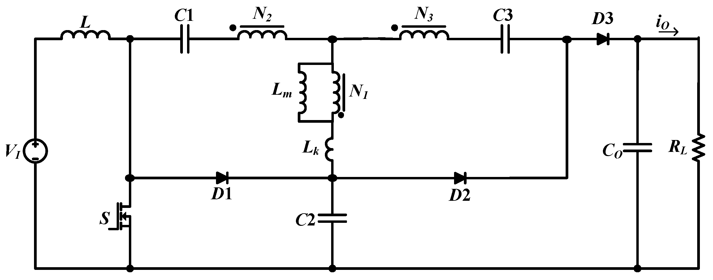
Figure 1 depicts the circuit configuration of the presented structure. As it is displayed in this figure, the converter comprises a three-winding coupled inductor, a single coil inductor, four capacitors, a power switch, and three diodes. In the presented converter, the diode
D1 and the capacitor
C2 act as the passive clamp circuit. The voltage stress on the power switch is limited to the voltage of the capacitor
C2. Additionally, the diode
D2 and the capacitor
C3 are the voltage multiplier cells that increases the output voltage gain. The inductor
L, at the input stage of the converter, regulates the input power and reduces the input current ripple. Therefore, a smooth current is drawn from the input power source. The presented converter has a star-connected three-winding coupled inductor. When the three-winding coupled inductor is charged, the actual turn ratio is decreased. However, when this inductor is discharged, the actual turn ratio is increased to enhance the output voltage gain ratio.
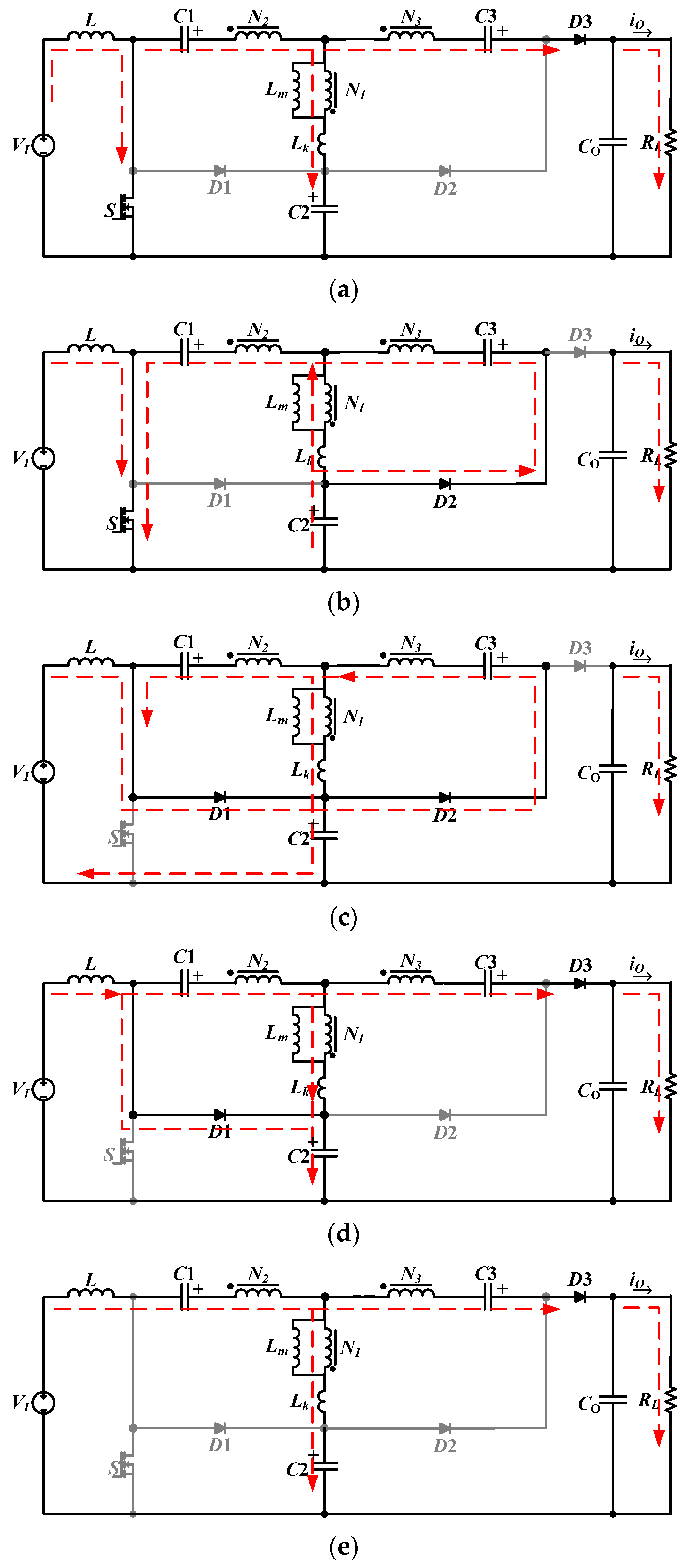
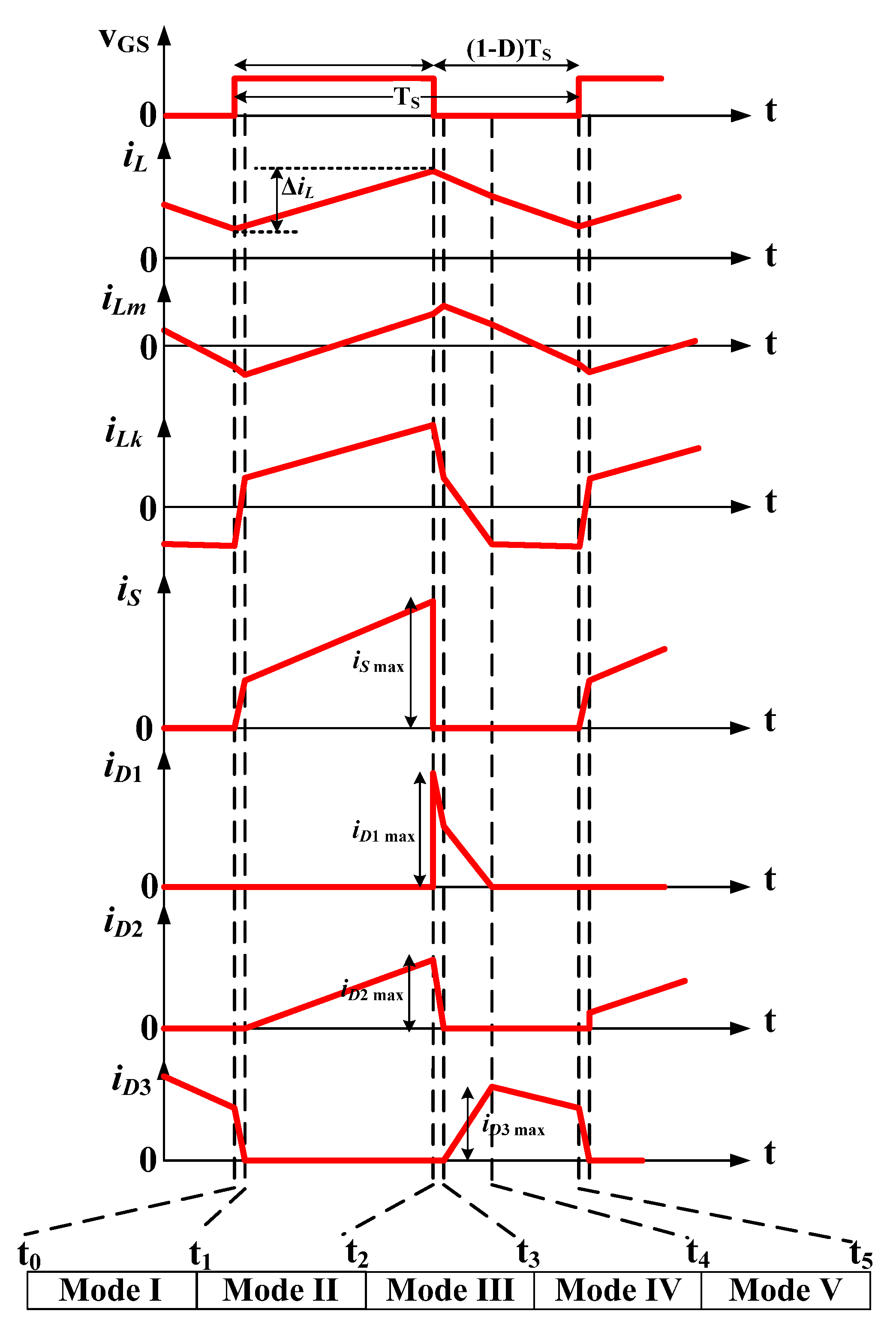
The steady state operation of the proposed converter is analyzed below. In the continuous conduction mode (CCM), five operation modes appear. The current flow paths of these modes are shown in
Figure 2. Moreover, several waveforms of the presented structure are depicted in
Figure 3. The voltages ripples of the capacitors are ignored so that we could simplify the analysis. Detailed and further analyses and explanations are as follows [
23,
24].
Mode I (
Figure 2a): In the first operation mode, the power switch
S is turned ON. The inductor
L is charged by the input voltage. The diodes
D1 and
D2 are reversed biased, but the diode
D3 is turned ON to conduct the current of the third winding of the coupled inductor. The output capacitor is charged by the same current of diode
D3. This operation mode is very short, and it ends when the current of the third winding of the coupled inductor reverses.
Mode II (
Figure 2b): In the time interval, the current direction of the third winding of the coupled inductor changes. Therefore, the diode
D3 is turned OFF while the diode
D2 is switched ON. In this mode, the magnetizing inductor Lm is charged by the capacitors
C1 and
C2. The output capacitor is discharged to supply the output load. The capacitor
C3 is charged by the current of the third winding of the coupled inductor. This mode finishes when the power switch is switched OFF.
Mode III (
Figure 2c): In this time interval, the switch
S is switched OFF. Therefore, the diode
D1 is turned ON to conduct the inductor current (
iL). In this mode, the passive clamp circuit is active, and the voltage stress of the power switch is limited to V
C2. This time interval is also very short, and it ends once the current of the third winding of the coupled inductor reverses and the diode
D2 is turned OFF.
Mode IV (
Figure 2d): In this interval, the diode
D3 is turned ON. Therefore, the current of the third winding of the coupled inductor charges the output capacitor. The magnetizing inductor is discharged by the capacitor
C1. This operation mode ends as soon as the diode
D1 is turned OFF.
Mode V (
Figure 2e): This mode starts when the inductor current (
iL) equals with the current of the second winding of the coupled inductor. Thus, the diode
D1 is switched OFF. In this mode, the capacitors
C1 and
C3 are discharged and the capacitors
C2 and
CO are charged. This mode ends when the switching period finishes, and the power switch is turned ON again in the following switching cycle.
The typical waveforms of the presented converter are illustrated in
Figure 3. For the steady-state operation of the proposed converter, stages I and III are ignored since these are very small and short in comparison to other stages.
According to
Figure 2b, the voltage across the inductor
L and the magnetizing inductor of the coupled inductor is as follows:
In mode IV (
Figure 2d), the voltages of the inductors can be stated as below:
Similar to the above analysis, the voltage across the magnetizing inductor is obtained in the fifth operation mode (
Figure 2e). In addition, Equation (8) can be derived by applying the KVL rule according to the figure. The equations are as follows.
By substituting and simplifying the (5) into (8), the voltage of the inductor
L in mode
V can be derived as below:
According to the voltage-second balance principle on inductors, the voltage of the capacitor C
2 can be calculated.
By substituting (9) into (8), the voltage of the magnetizing inductor in mode
V will be as below:
Similar to the inductor
L, the voltage-second balance principle is applied to the magnetizing inductor and the voltage of the capacitor
C1 is derived.
By substituting Equations (10) and (12) into (2), and simplifying with (3), the voltage of the capacitor
C3 can be expressed.
Using Equations (7), (8), (10), (12), and (13), and simplifying the equations, the output voltage can be calculated.
where
M is the voltage gain of the proposed converter. The output voltage gain is calculated in Equation (14). It is very important to mention that the voltage gain equation shows the unique operation of the three-winding coupled inductor. According to (14), it is possible to draw a schematic for the three-winding coupled inductor. The schematic is shown in
Figure 4.
As it is shown in
Figure 4, the additional winding (
N2) is subtracted from the primary side of the coupled inductor. In addition, the secondary side of the coupled inductor is increased by the proper connection of the windings
N1 and
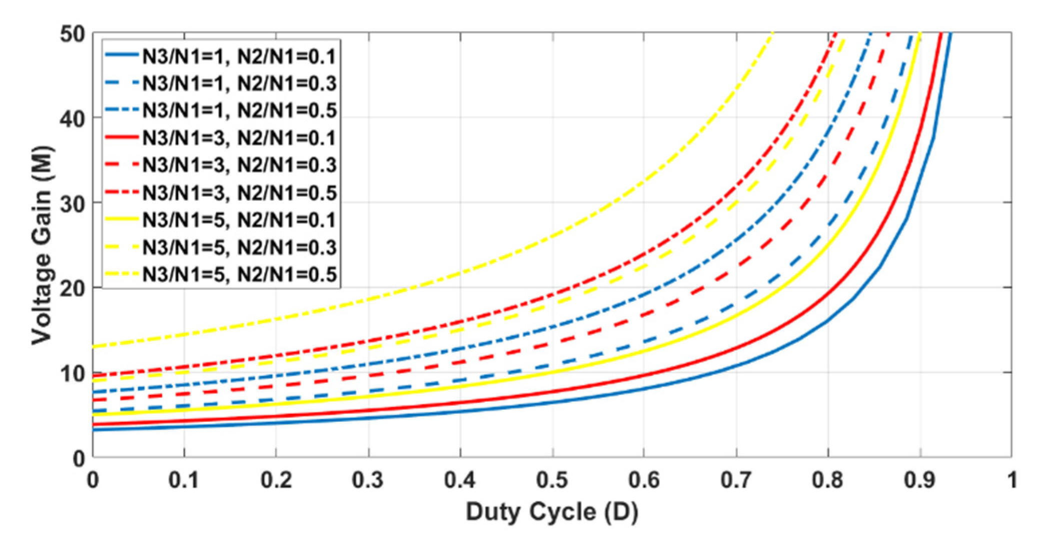
N3. This unique feature increases the voltage gain of the presented converter. The voltage gain of the converter is depicted in
Figure 5. In this figure, the voltage gain is illustrated for the different values of
N2/
N1 and
N3/
N1 turn ratios.
In
Figure 5, the effect of the additional winding on the coupled inductor is obvious. As it is shown, the presented converter has a high output voltage gain ratio. The converter design is also very important for the proper operation of the presented converter. Therefore, the next section is devoted for converter design procedure.
3. Converter Design Considerations
In this section, the presented converter is analyzed so that the design criteria could be derived. This section focuses on the optimum design and selection of the capacitors, inductors, diodes, and the power switch in order to achieve an acceptable performance.
First, the minimum values of the inductors must be calculated so that the presented converter operates in Continuous Conduction Mode (CCM). The Discontinuous Conduction Mode (DCM) must be prevented since it has various drawbacks such as the dependency of the output voltage on the frequency and the load, slow dynamic response.
In [
23,
24], it is discussed the average current of an inductor must be more than half of its current ripple for CCM [
3]. The current ripple of the inductors
L and the average current of the inductor L can be written according to
Figure 3.
where
M is the voltage gain. By applying the aforementioned principle, the least possible value of the inductor
L can be expressed as below:
According to
Figure 3, the current ripple of the inductor
Lm can be expressed as follows.
In order to find the average value of the magnetizing inductor current, the ampere-second balance principle is applied to the capacitor
C1. The capacitor current
C1 can be expressed as follows:
Assuming that the average value of all diode currents is the output current (
IO), and applying the ampere-second balance principle, the following can be deduced that:
In order to realize the minimum value of the inductor
Lm, the BCM (Boundary Conduction Mode) should be discussed. At the end of the switching period in BCM mode, the diode
D3 will be turned OFF. In other words, at the end of the switching period, the
iL = –
iLk. Therefore, the following equations can be derived:
In BCM mode, when the diode
D3 is turned OFF at the end of the switching period, the minimum value of the magnetizing inductor current is equal with the:
The peak value of the magnetizing inductor is also can be expressed as follows:
To ensure the CCM operation of the presented converter, the equation below must be satisfied:
Therefore, using (16), (18), and (24), the minimum value of the inductor Lm can be calculated:
The voltage stresses on the semiconductors are very important for a proper design. Therefore, it is crucial to calculate the reverse voltage on the semiconductors.
The current stresses of the semiconductors are very important alongside their voltage stresses. The maximum current flowing from a semiconductor is a crucial criterion to select the proper device. In order to calculate the maximum current stresses of the semiconductors, the current-second balance principle can be applied to the capacitors. Therefore, it can be obtained that the average current of all diodes is equal with the output current. Considering
Figure 3, the average current of the diode
D2 can be expressed as follows:
Considering the above equation, the maximum current of the diode
D2 can be derived.
According to
Figure 3, the maximum current of the power switch happens at the end of the mode II. In this mode, the maximum current flowing from the power switch can be derived as below.
Substituting Equations (15) and (16) into the above equation and neglecting the current ripple across the inductor
L, the maximum current of the power switch can be obtained as follows:
In the beginning of the mode III, when the power switch is turned OFF, the maximum current of the power switch flows from the diode
D1. Therefore, the maximum current flowing from the diode
D1 is equal to the maximum current of the power switch as below:
The ratio of mode IV time interval to the switching period (
d4) can be calculated considering that the average current of all the diodes are equal to the output current.
Where d4 is the ratio of mode IV time interval to the switching period. Substituting (32) into (33), the
d4 can be derived as below.
In order to find the current stress of the diode
D3, the average current of the diode
D3, according to
Figure 3, can be obtained.
The maximum current of the diode
D3 can also be calculated as follows:
The output capacitor shall also be designed the meet the maximum allowed voltage ripple requirements. The output capacitor can be modeled as an ideal capacitor and an
ESR (equivalent series resistance). As a result, the voltage ripple across the capacitor will be the sum of the voltage ripple across the ideal capacitor and the
ESR. The voltage ripple across the ideal capacitor is calculated as follows:
The current flowing from the output capacitor can be written as below.
Therefore, the maximum current ripple of the output capacitor is the peak current of the diode
D3. Considering the equations below, the voltage ripple across the
ESR of the output capacitor can be expresses.
As a result, the total voltage ripple across the capacitor can be expressed as follows:
By considering the maximum value for the allowed voltage ripple across the output capacitor, the minimum value of the output capacitor can be derived. By considering the above criteria, a suitable converter can be designed for various applications with proper operation.
4. Loss Analysis of Proposed Converter
In this section, the theoretical calculation of the converter efficiency is provided. To simplify the calculation of the efficiency, some assumptions are considered. The voltage ripple across the capacitors and the current ripple across the inductors are neglected. In addition, the leakage inductance of the coupled inductor is also ignored. In order to derive the efficiency of the converter, the
RMS values of the currents shall be calculated. The
RMS values of the diode currents can be calculated as follows:
The total power loss on the forward resistances of the diodes (
rD) can be calculated in below:
The forward voltage of the diodes (
VF) also causes some power losses. As the average currents of all diodes are
IO, the power losses can be calculated as follows:
In order to calculate the power losses of the main switch, it is important to find the
RMS value of the switch current. The
RMS value of the switch current can be derived.
According to [
3], the switching loss of the main switch can be expressed as follows:
where
fS is the switching frequency and
Cs is the parasitic capacitance of the main power switch (MOSFET). Therefore, the overall power loss of the power switch can be calculated as below:
The equal series resistance of the inductor
L also causes some power loss. Since the current ripples across the inductors are neglected, the
RMS value of the inductor
L current is equal with its average value. The power loss can be expressed as follows:
By neglecting the operation modes I and III, the current of the primary side of the coupled inductor can be stated as follows:
Therefore, the overall power loss of the coupled inductor can be calculated.
where
rCI is the total equivalent resistance of the coupled inductor.
The
RMS values of the capacitor currents shall be calculated to obtain the total loss on capacitors as well. The capacitor currents can be expressed as follows.
According to the above equations and Equations (38)–(40), the
RMS values of the capacitors can be calculated.
The capacitor losses can be derived as follows:
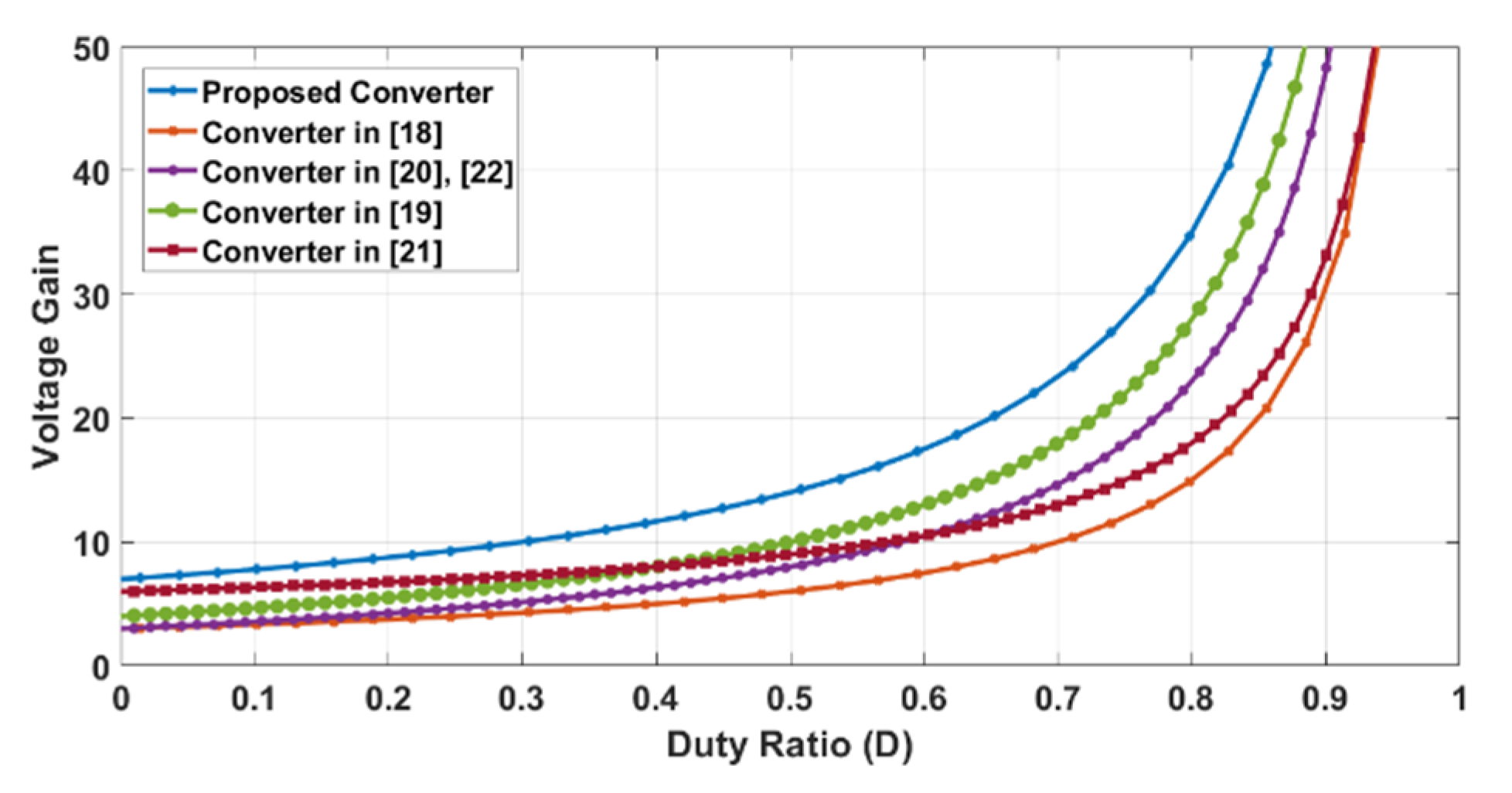
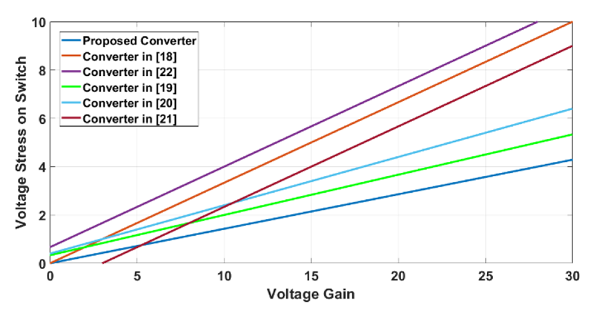
5. Comparisons
In order to demonstrate the superiority of the presented converter, some comparisons shall be made. Some converter recently presented in the literature are compared with the presented structure from the output voltage gain aspect. The results are shown in
Figure 6. As it is depicted in the figure, the presented converter has a higher output voltage conversion ratio. This is an advantage for the presented converter since the presented converter can reach the desired output voltage with lower duty cycles. In addition, the voltage stress on the main switch is another aspect for comparison. The voltage stresses on the main switches are compared in
Figure 7. According to
Figure 7, the voltage stress of the presented converter is lower than the presented converters in the literature. A low on-state resistance power switch can reduce the conduction loss on the main switch.
A similar converter is also presented in [
27]. In this converter, the coupled-inductor is located in the input stage of the converter. Due to the small size of the leakage inductor of the coupled-inductor, large current fluctuations and ripples will appear in the input stage of the converter which is a great drawback in renewable energy applications, or and input current filter is required which will decrease the conversion efficiency of the converter.
In addition, in [
28,
29], the voltage gain is improved with obtaining a continuous input current. However, more components, diodes and capacitors, are used in the circuit structures.
A general overview of the compared structures is provided in
Table 1.
Table 1 summarizes the number of semiconductors in each structure, voltage gain, voltage stress and the continuous input current aspect. According to the provided information, the presented converter is suitable for various applications such as fuel cells. Due to fuel cells slow dynamic response, high input current ripple will deteriorate the operation of the fuel cells.
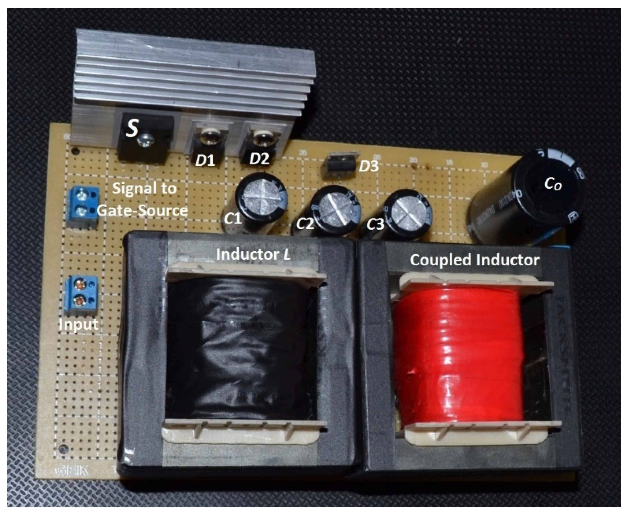
6. Experimental Results
In order to obtain the experimental results, a 250 W prototype circuit is implemented in the laboratory. Hardware specifications are summarized in
Table 2. The picture of the implemented prototype is shown in
Figure 8.
It is useful to note that the switching frequency (33 kHz) ensures the CCM operation of the converter in the nominal load conditions (250 W). Therefore, the switching frequency is not increased further to reduce the switching loss on the main switch (S1).
Figure 9 depicts the obtained experimental results. The turn ratio of the coupled inductor is selected as
N3/N1 = 2,
N2/N1 = 0.4. In
Figure 9a, the voltages of the capacitors are shown. It is important to note that the duty ratio is 65 percent. The voltage of the capacitor
C1,
C2,
C3, and
CO are approximately 51, 76, 114.5, and 400 V, respectively. The obtained result validates the steady-state analysis of the presented converter. In
Figure 9b, the voltage stress across the power switch and diode
D1 are shown. When the power switch is turned OFF, the active clamp circuit becomes active and limits the maximum reverse voltage on the switch to the voltage of the capacitor
C2. Therefore, as it is depicted in the figure, the voltage stress on the main switch and the diode
D1 are 76 V. In
Figure 9c, the voltage stress of the diode
D3 is shown. As it can be seen, the voltage stress is about 350 V.
Figure 9d illustrates the current stress of the power switch and the diode
D1. The maximum current flowing from the power switch and the diode
D1 is about 20 A. In addition, the inductor current
L and
Lk are shown in
Figure 9e. As it is shown, the inductor current
iL fluctuates between 9.8 and 11.4 A. This shows the continuous input current characteristic of the presented converter. This current is drawn from the input power source, which is very favorable for renewable energy applications. Furthermore, the current waveform of the
Lk is in accordance with the analysis in
Figure 3. The current waveform of the diode
D2 is also shown in
Figure 9f. As it is shown, the current reaches its peak value at 1.58 A.
All in all, the experimental results prove the efficient operation and the feasibility of the proposed structure.
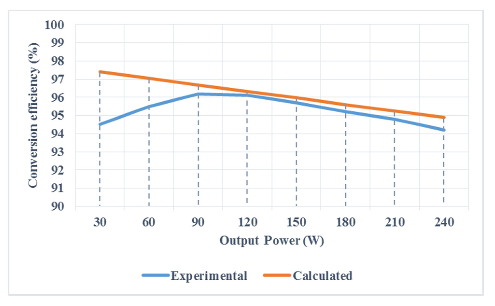
In order to calculate the efficiency, the voltage drop on the power diodes is considered to be 1.5 V and the on-state resistance are 0.002 Ω. The on-state resistance of the power switch is about 0.06 Ω in 80 °C. The resistance of the inductor L is considered to be 0.01 Ω. The equal resistance of the coupled inductor is deemed to be 0.02 Ω. The efficiency of the converter is calculated in different output power levels which shows that the presented converter can reach high efficiency values of 96% in its nominal load conditions. In addition, the efficiency is obtained in the experiment. The obtained results are shown in
Figure 10. It should be noted that the difference in the calculated and experimental efficiency in the light load condition is caused by the discontinuous operation (DCM) of the presented converter in the light load condition. As the output power is increased and the output power is closer to the nominal power, the converter operates in the continuous operation mode (CCM), and the obtained results are nearer. According to the figure, the converter has a satisfactory conversion efficiency.

 ,
, 


