Conversion of power from DC to AC or AC to DC is a key technology involved in the generation, transmission, distribution, and utilization of electrical energy. With the advent of fast and high rating power electronics devices, digital controllers, and sensors the power converter industry is seeing a revolution. Inverters form the backbone of drives and grid integration applications. They can be classified based on the nature of the output waveform, such as square wave inverter, quasi square wave inverter, two-level pulse width modulated inverters, and multilevel inverter [
1,
2]. Although the realization of conventional two-level inverters is simple, it has many shortcomings. High total harmonic distortion (THD) with the requirement of higher blocking voltage rating devices and the better design of filters for improving the power quality restrict their application to a small power range. To overcome the shortcomings of the conventional two-level inverter, a multilevel inverter was proposed [
3,
4,
5]. Multilevel inverters are composed of semiconductor switches and DC power supplies/capacitive voltage sources. A multiple-step voltage waveform with variable and controllable frequency, phase, and amplitude are obtained by suitable connection and control of the switches using a modulation scheme [
6]. Because of the inherent superior harmonic profile and less voltage stress across switches, MLI has replaced a two-level counterpart for high power applications. MLIs find wide usage in motor drive applications [
7]. Neutral point clamped (NPC), flying capacitor (FC), and cascade H bridge (CHB) are the conventional MLI topologies. Separate DC voltage sources are required for the generation of multistep voltage in a CHB. CHB has a modular structure and can be more easily extended to achieve higher voltage levels. FC requires a complex control mechanism to ensure that the voltage across the capacitor is maintained constant. Therefore, conventional MLI is not suitable for voltage levels beyond five [
8]. A large number of modified/hybrid conventional topologies that were proposed required a large number of power semiconductor switches for the generation of higher voltage levels [
9]. Each switch requires a separate driver circuit and heat sink. Consequently, size and complexity increase. To avoid these issues, authors in [
10,
11,
12,
13,
14] presented reduced device count topologies of MLI. Although a higher number of voltage levels are generated with a smaller number of device counts, they do not possess the voltage boosting capability. This boosting feature is available in the switched capacitor multilevel inverter (SCMLI) in which the capacitor acts as a voltage source, which was introduced by authors of [
15] in 1998. They obtained a 31-level output voltage with the help of two sub-circuits. Each sub-circuit contained 15 basic cells. One basic cell consisted of two diodes, two MOSFETs, and one capacitor. The topology requires a complex control algorithm for balancing the capacitor voltage. Authors of [
16,
17] introduced reduced device count MLI topologies having a capacitor, but the capacitor voltage balancing issue remained. This problem was overcome by adding an auxiliary circuit reported in [
18,
19]. However, it increased the overall cost and complexity of the system. In [
20], authors developed a novel switched capacitor-multilevel inverter known as a Marx inverter. It is capable of synthesizing the different output voltage levels and also maintaining the capacitor voltage at the desired level. Seven level output voltage is obtained with the help of ten switches. By cascading SC cells (consist of switches and capacitors), higher voltage levels can be achieved. In [
21] authors proposed a new basic unit having two switches, one diode, and one capacitor. The topology has self-boosting capability without any transformer. Seventeen and twenty-five level output voltage with experimental results were reported. Since the boosting factor of this basic unit is two times of DC supply voltage, therefore for the generation of a higher number of voltage levels, cascading of basic units is needed. However, the cascading will increase the complexity and total standing voltage (TSV) of the circuit. Authors in [
22] presented a switched capacitor multilevel inverter; this circuit can generate higher number of voltage levels with fewer switches in asymmetric configuration, but the TSV of the structure is significant. By the simultaneous charging and discharging of capacitors, authors in [
23] obtained multilevel output voltage. However, it requires a large number of bidirectional switches and it also increases the TSV of the circuit significantly. In [
24], authors introduced a novel structure of the switched-capacitor multilevel inverter. Its basic unit generates nine level output voltage with the help of ten switches, two capacitors, one diode, and one DC supply. The extended structure of this switch capacitor multilevel inverter was also discussed for symmetric and asymmetric DC supply configurations. However, the structure again suffers from a high TSV level for a higher voltage level. Authors in [
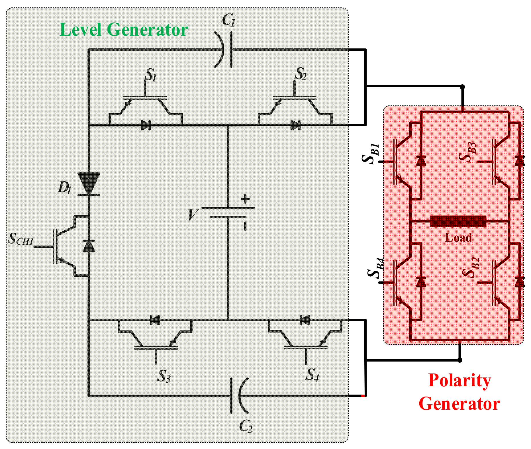
25] proposed a new basic unit cell where the boosting factor is three times the DC supply voltage with the help of five semiconductor switches, two capacitors, and one diode. The structure promises to be a competitive topology for SCMLI.
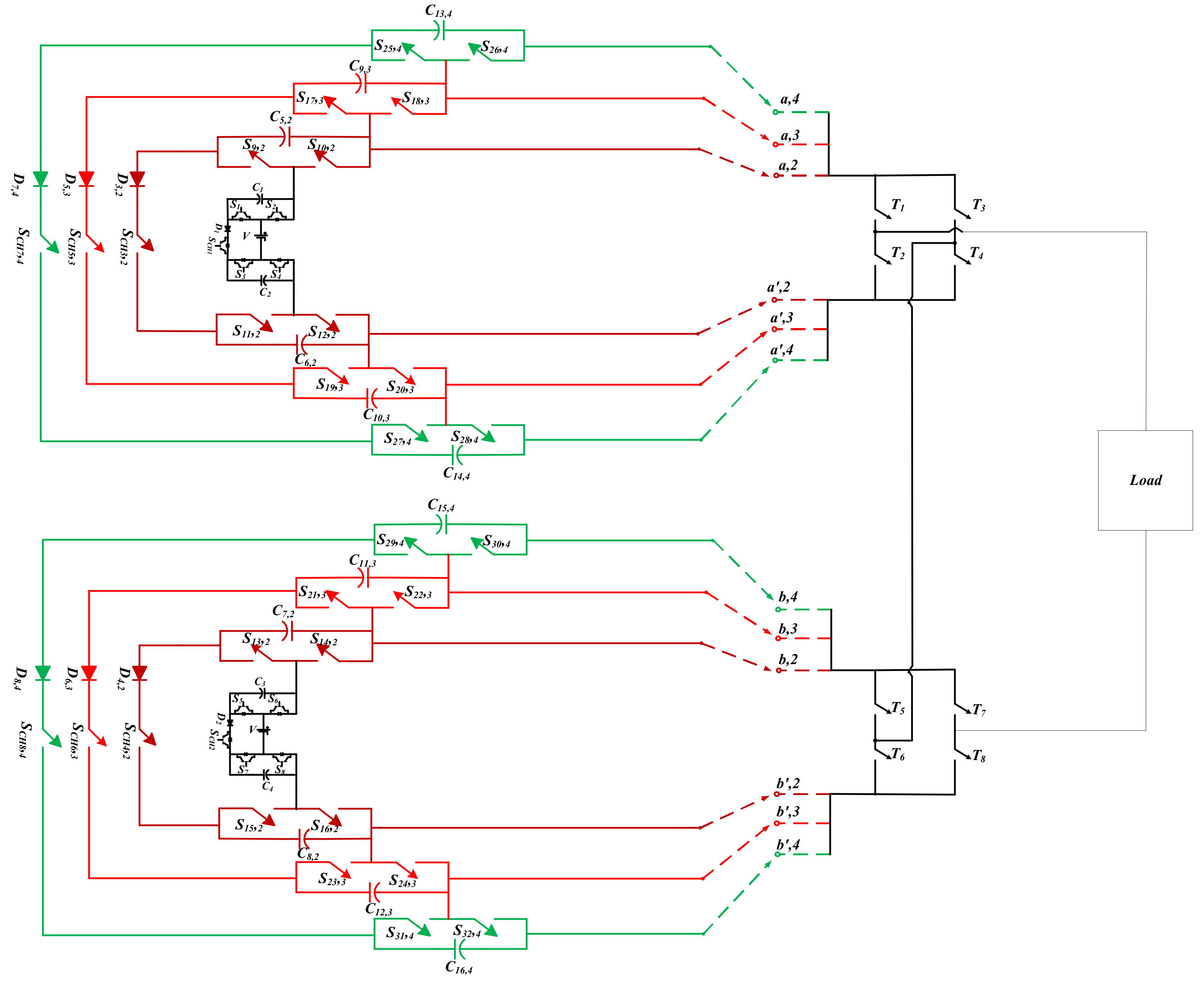
In this paper, a generalized topology taking the basic unit of [
25] is proposed. The paper is organized into eight sections. In
Section 1, the working of the basic unit is explained.
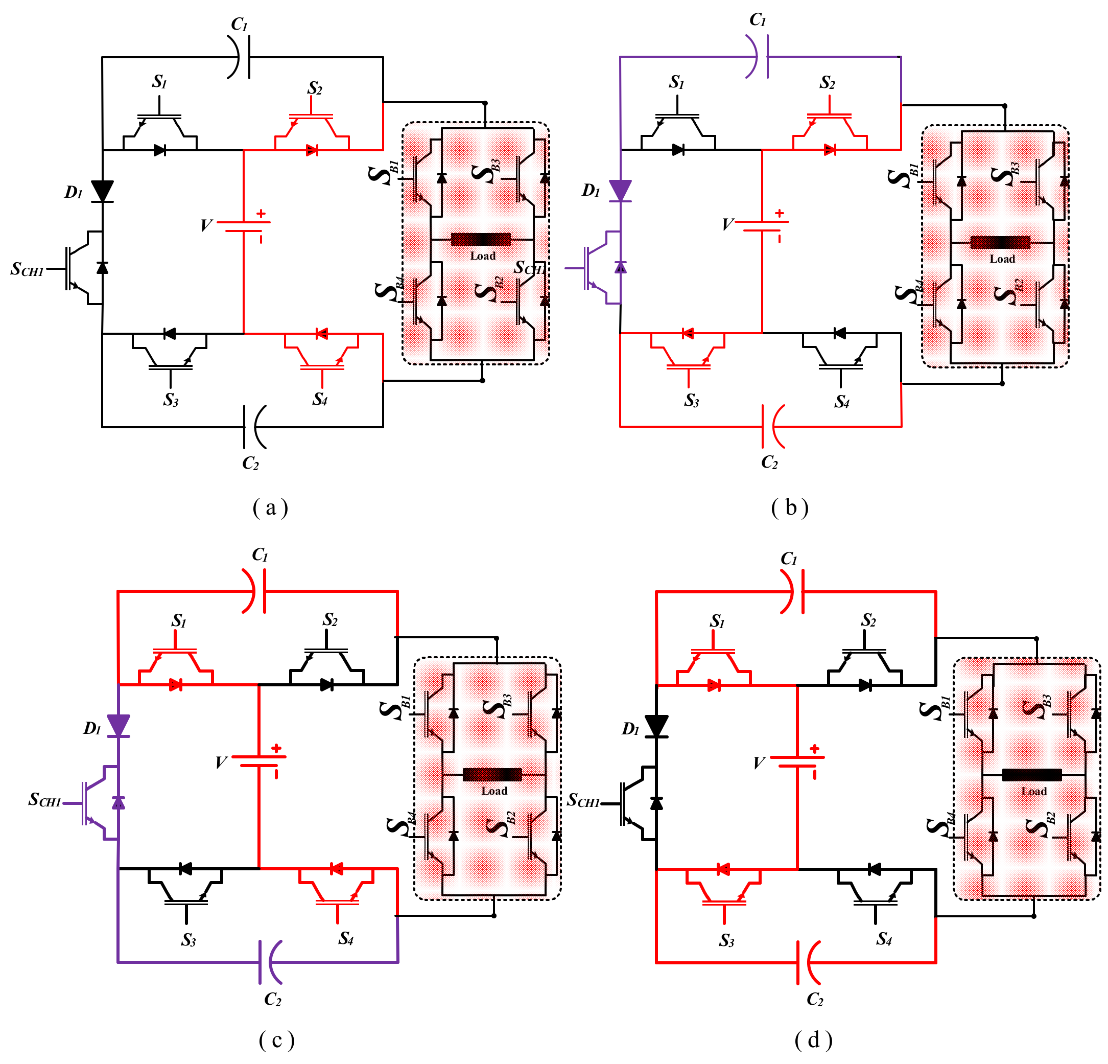
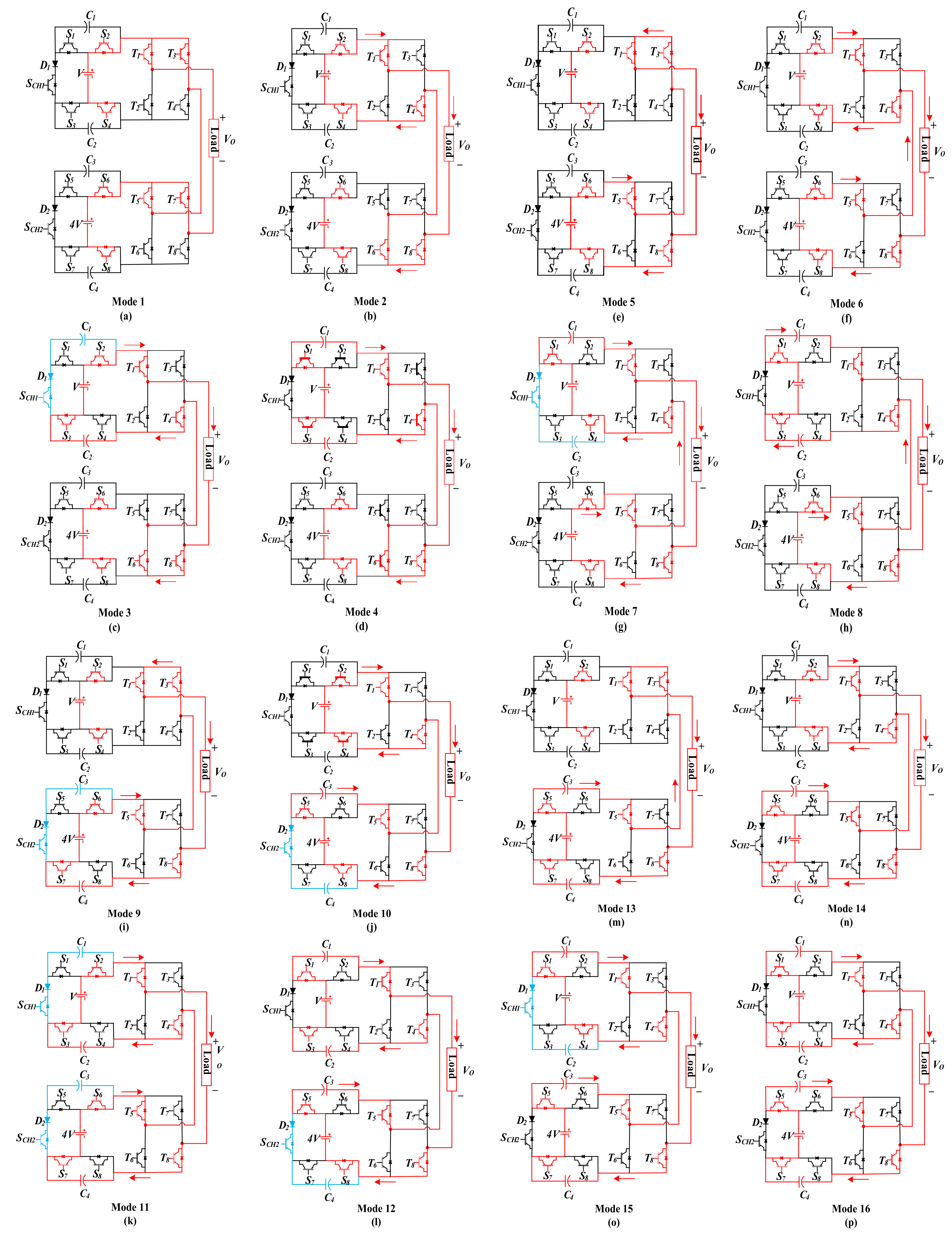
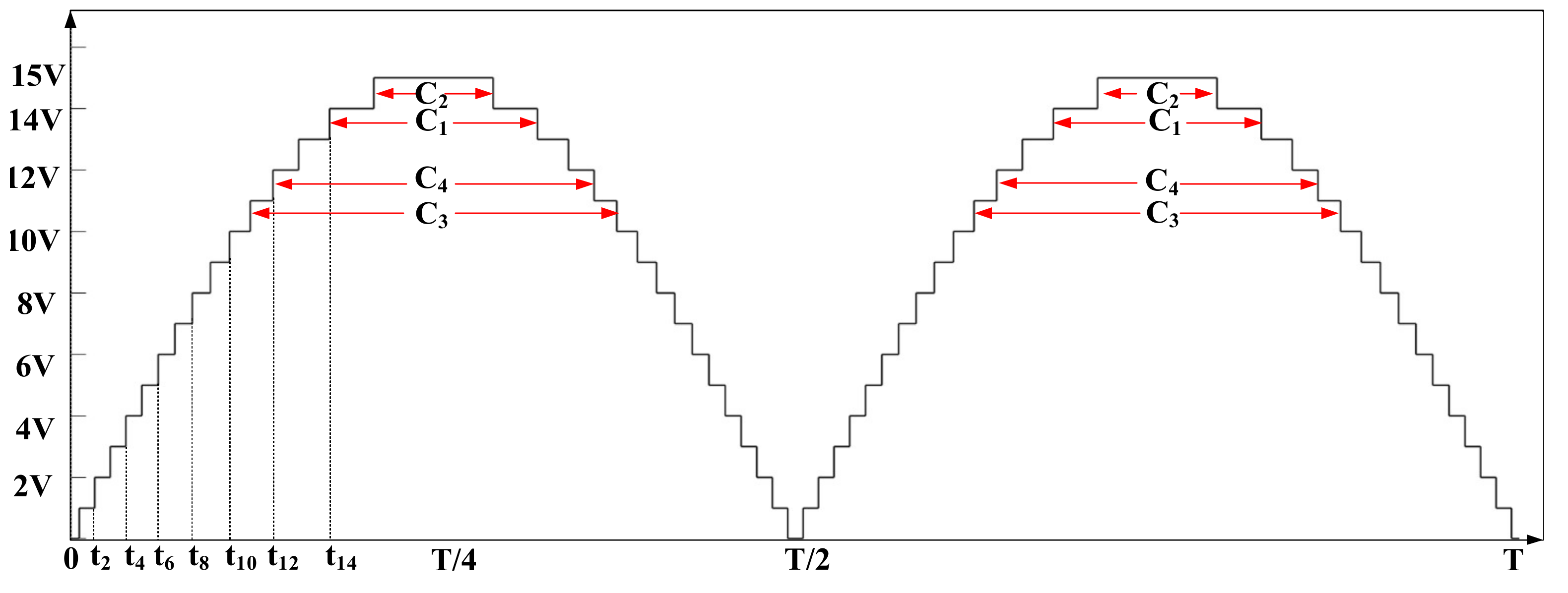
Section 2 deals with a symmetric DC supply configuration and its modes of operation. Further, in
Section 3,
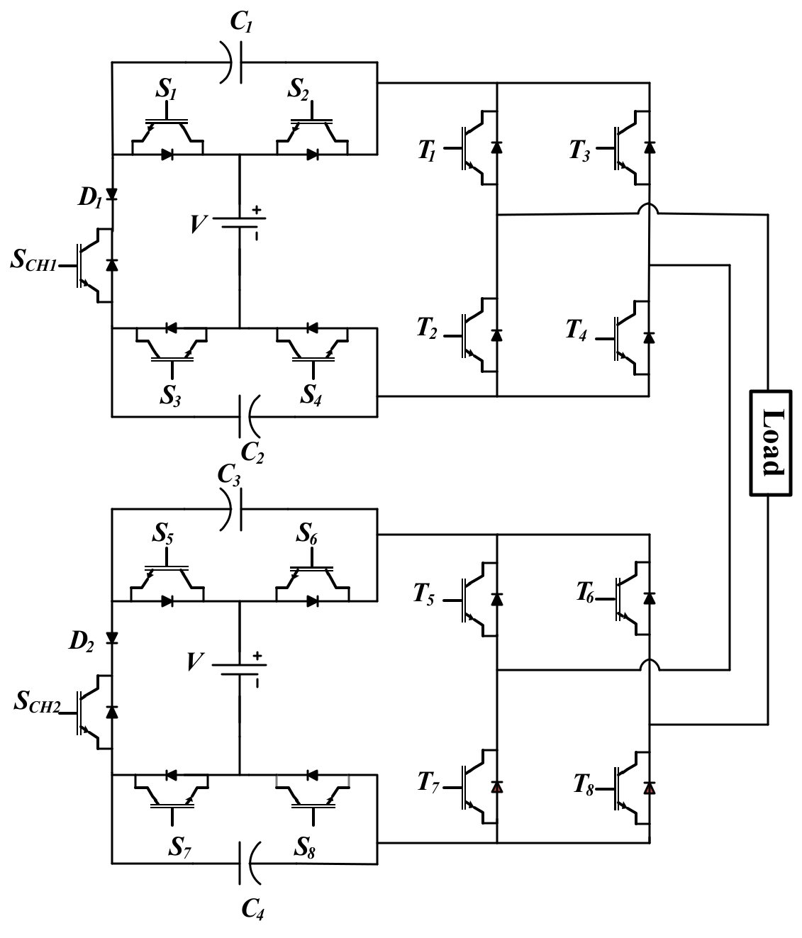
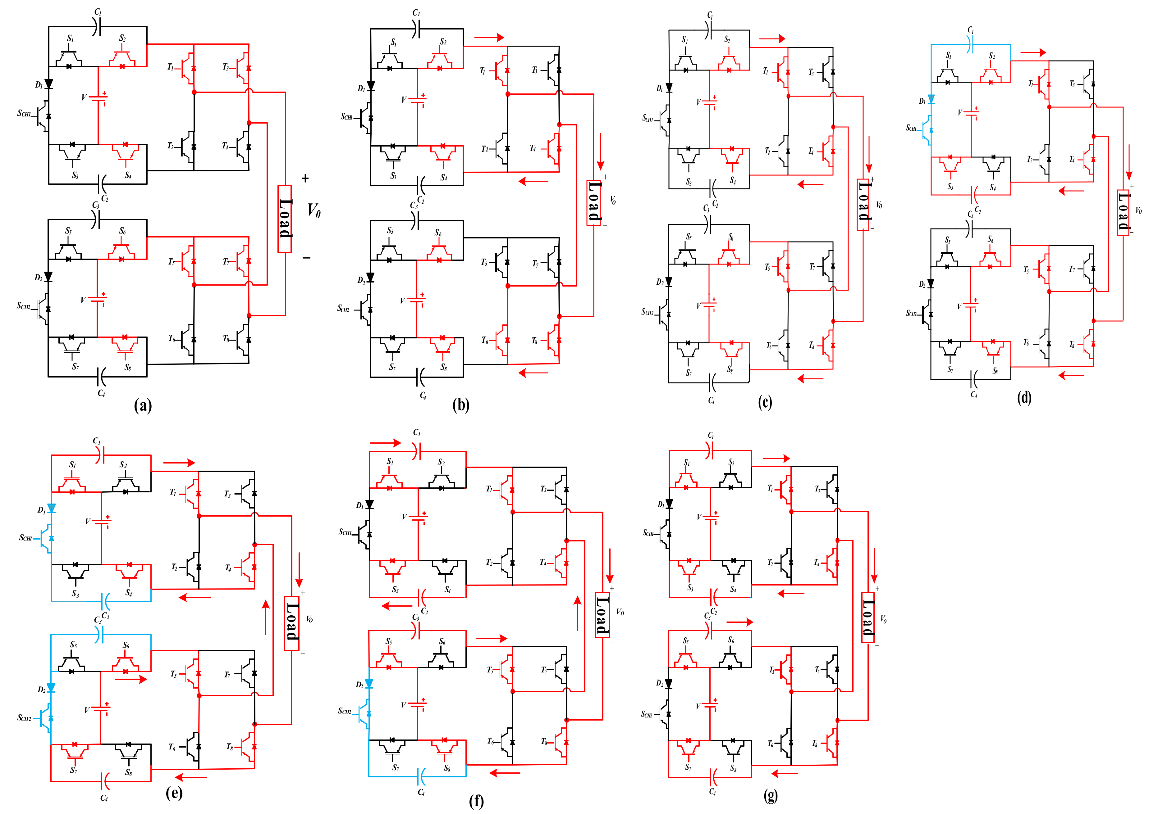
Section 4 and
Section 5, an asymmetric DC supply configuration, selection procedure of capacitance, and an extension of the proposed topology are discussed, while
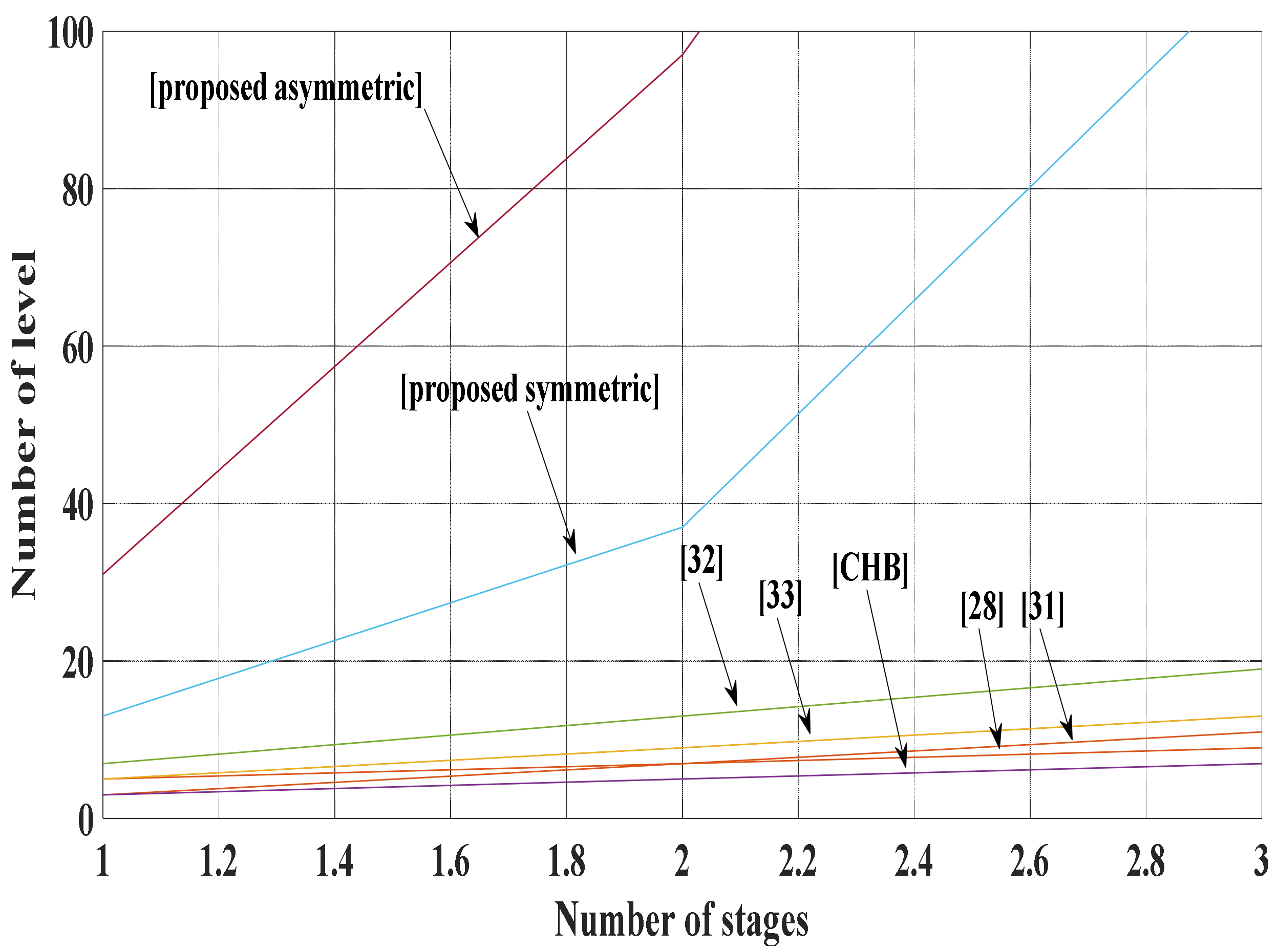
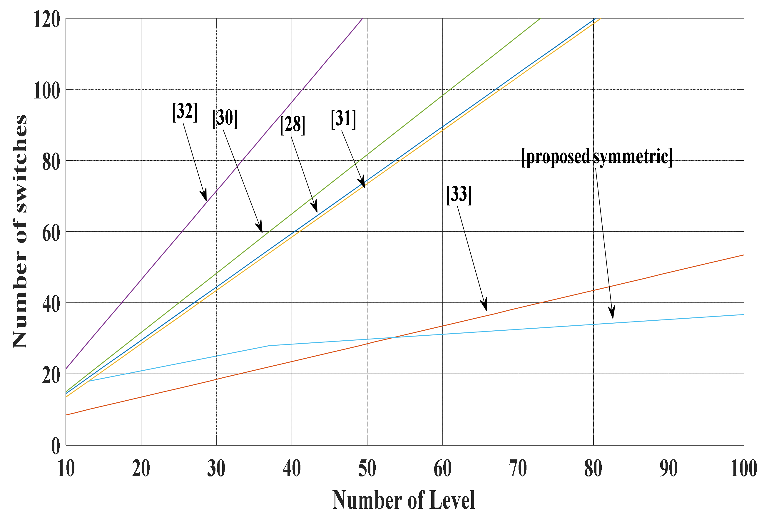
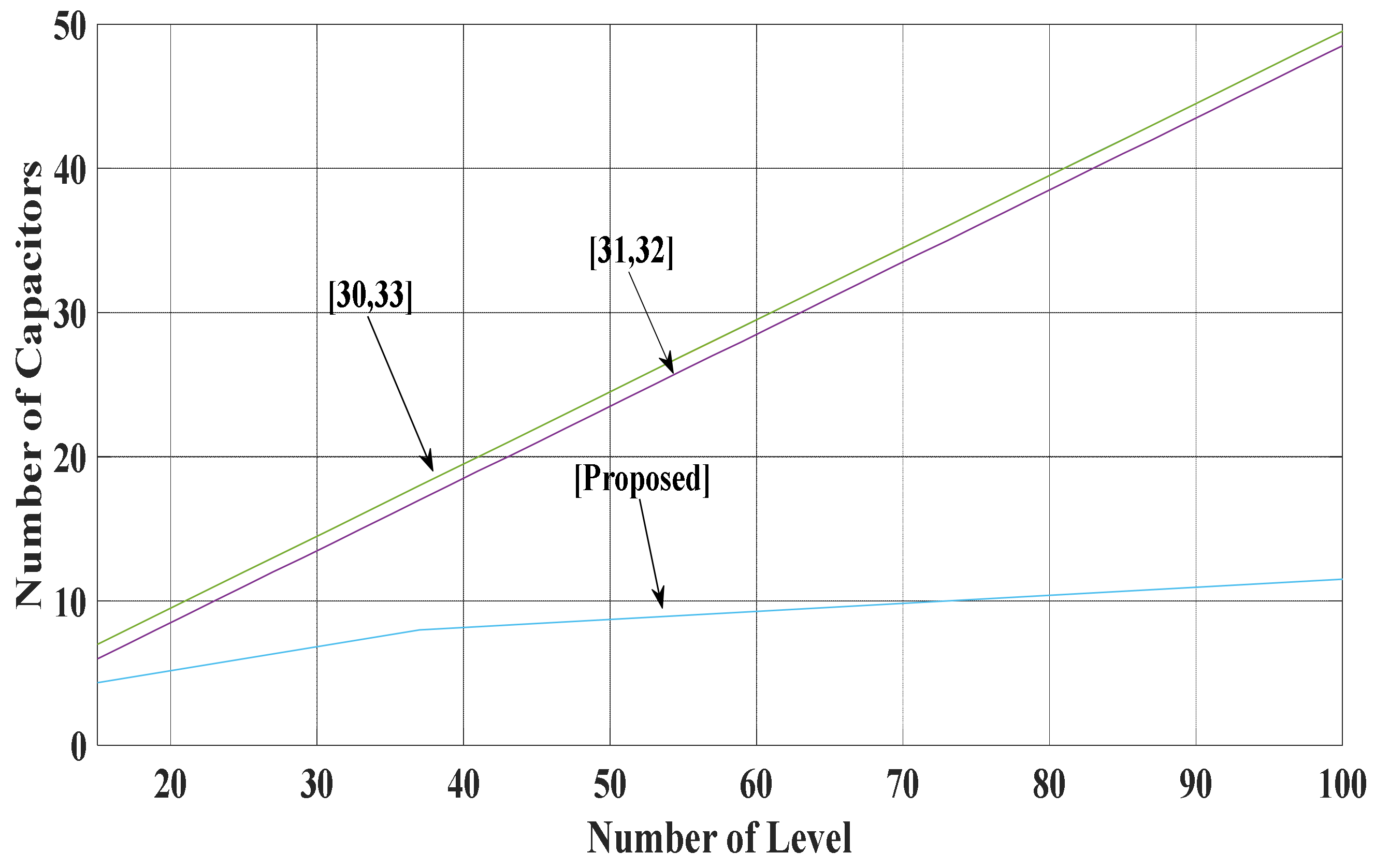
Section 6 deals with comparative analysis of the proposed generalized scheme.
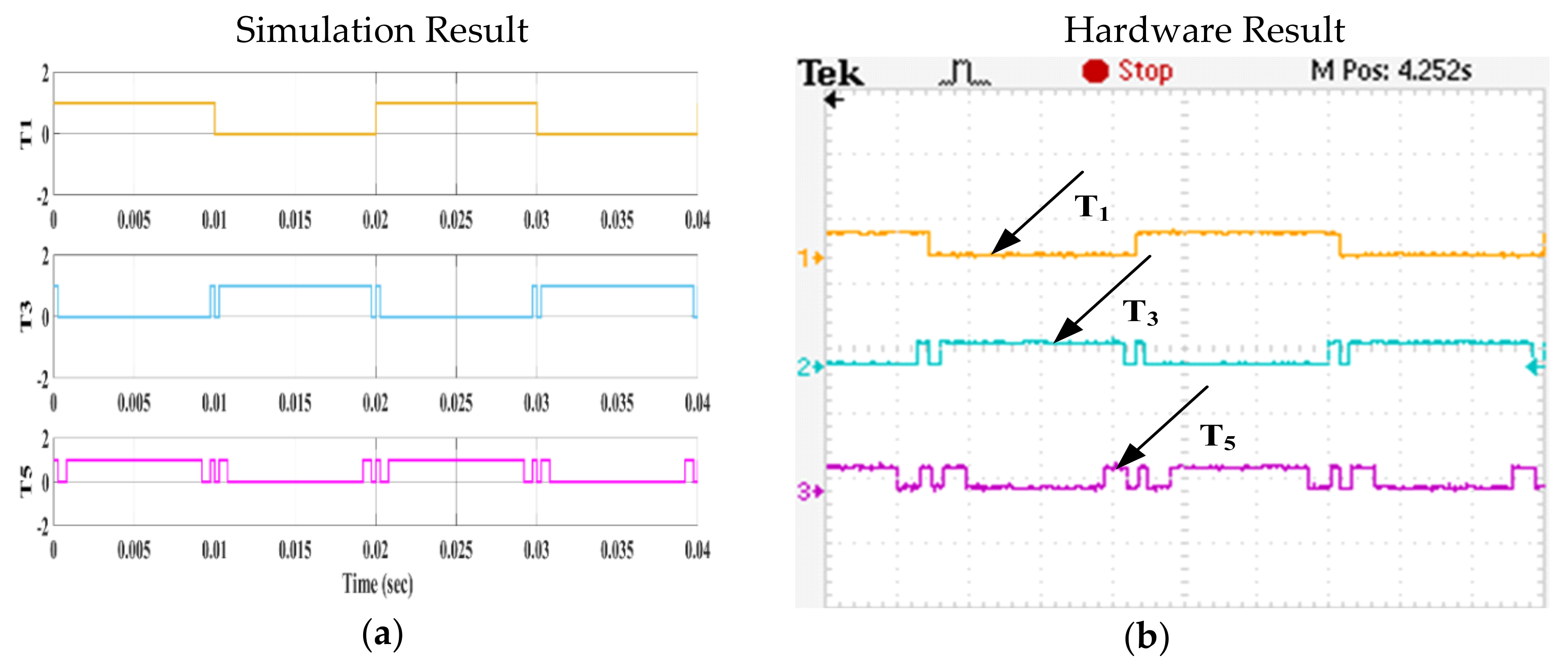
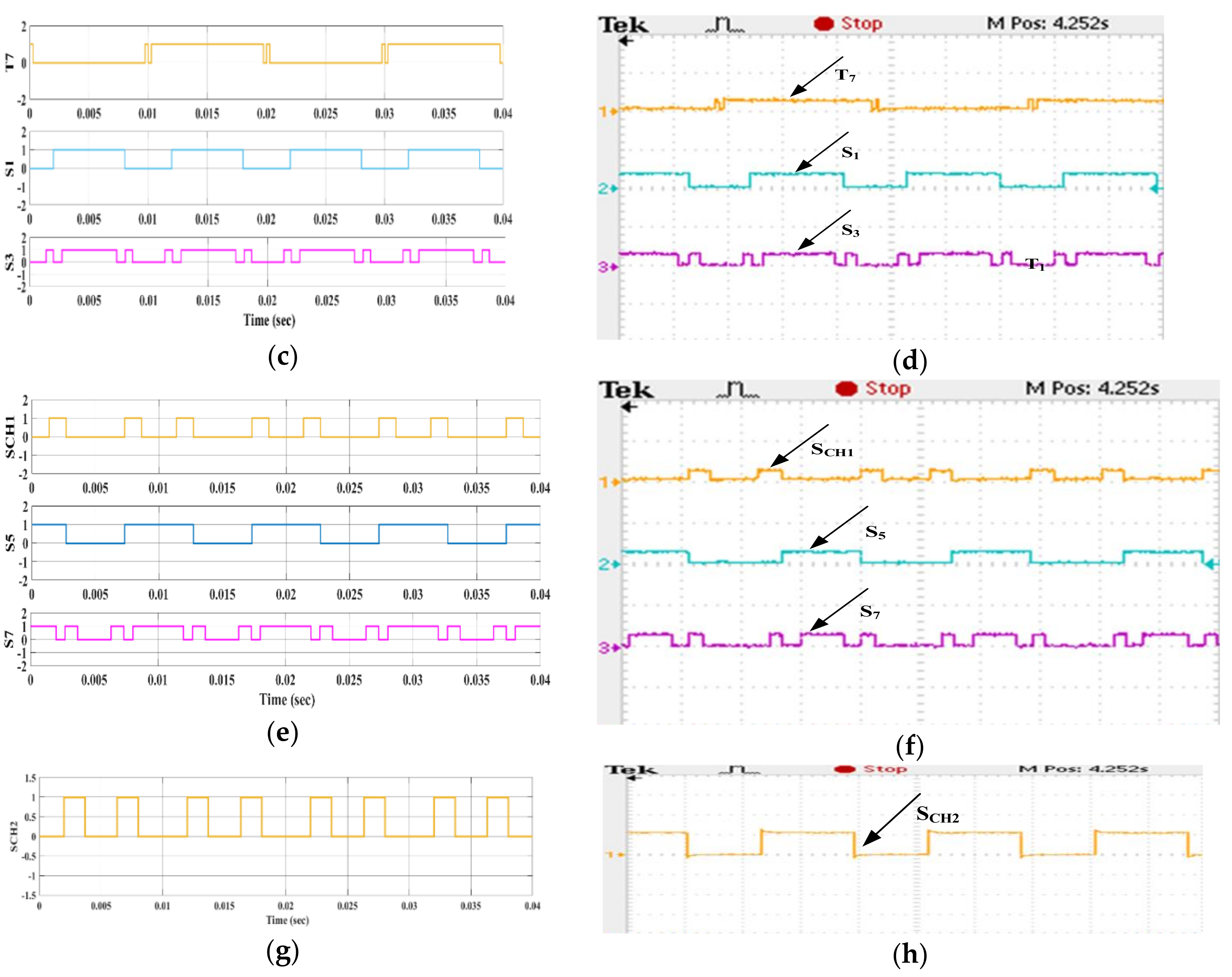
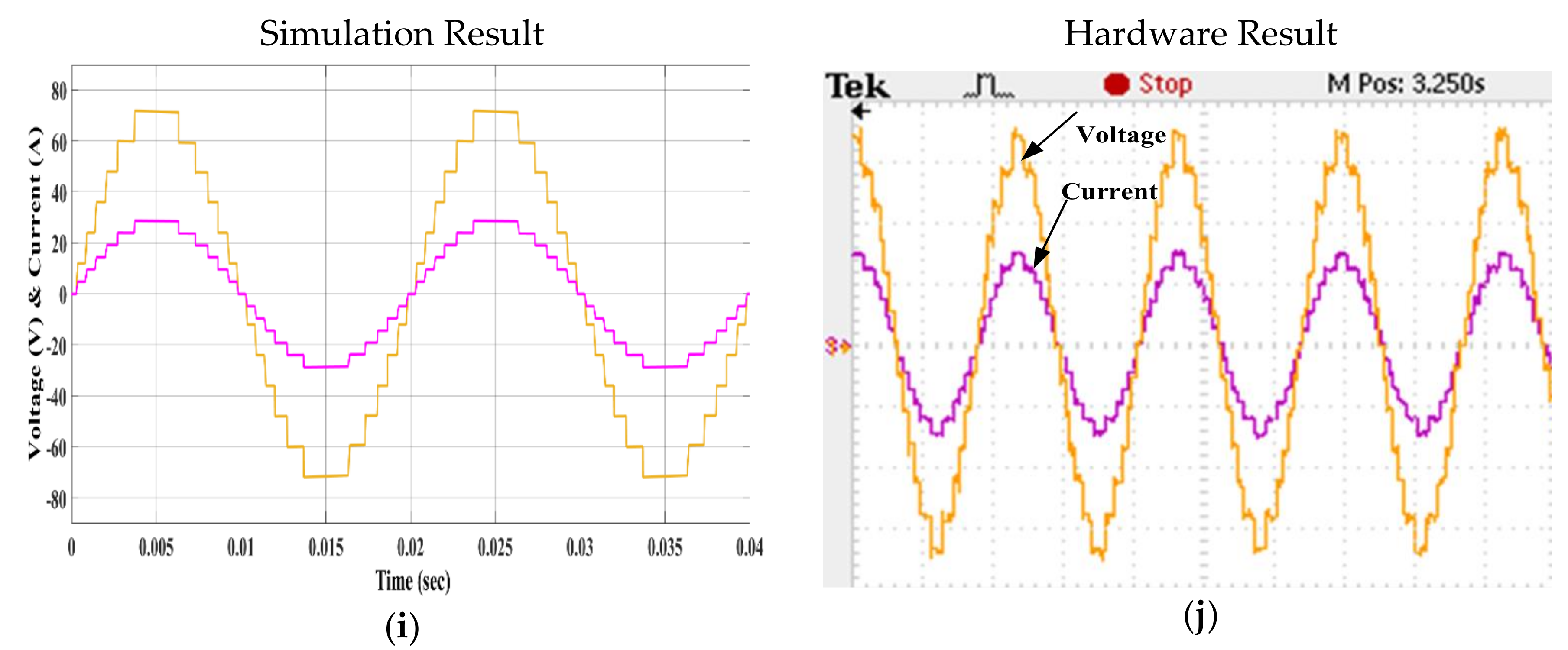
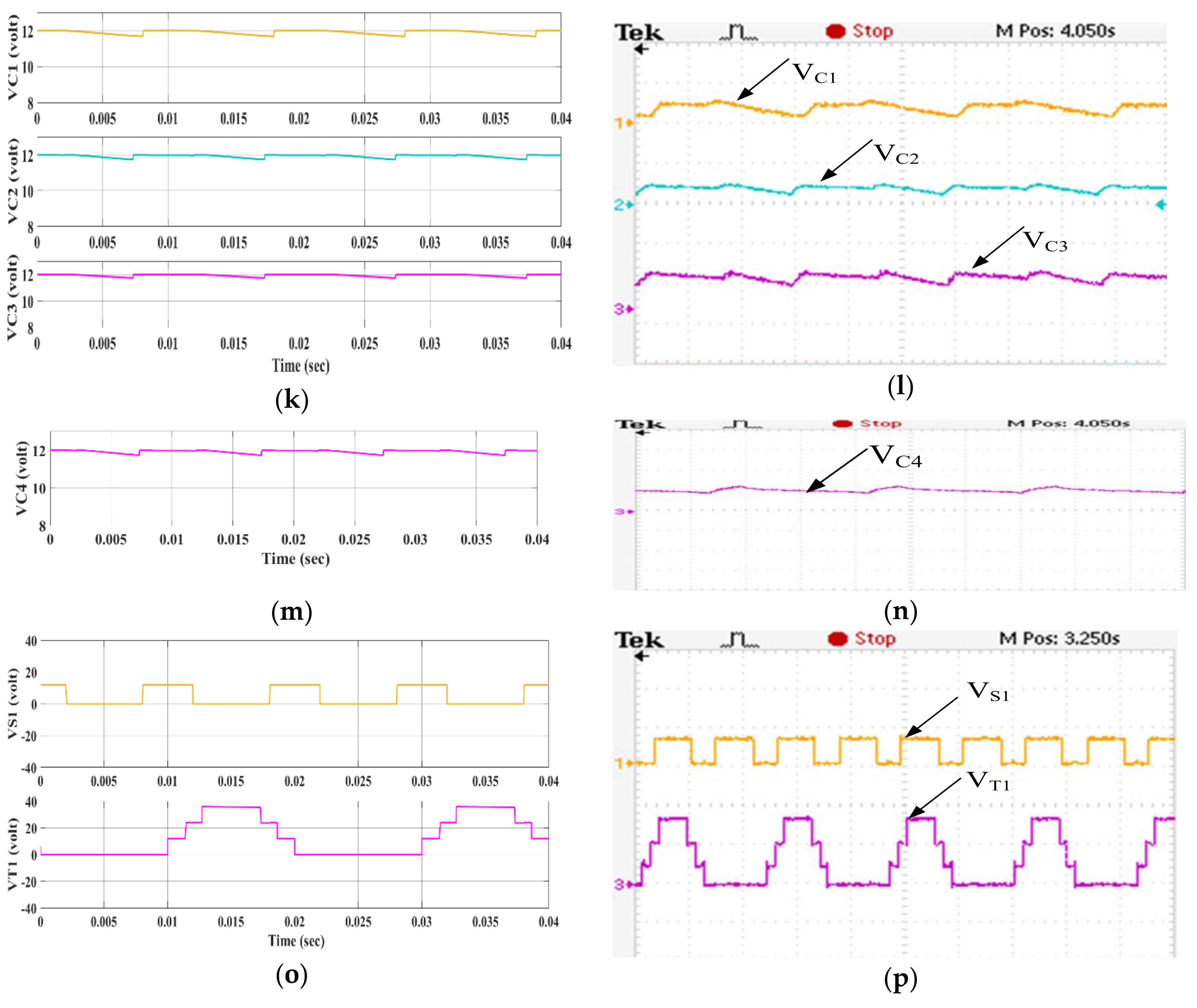
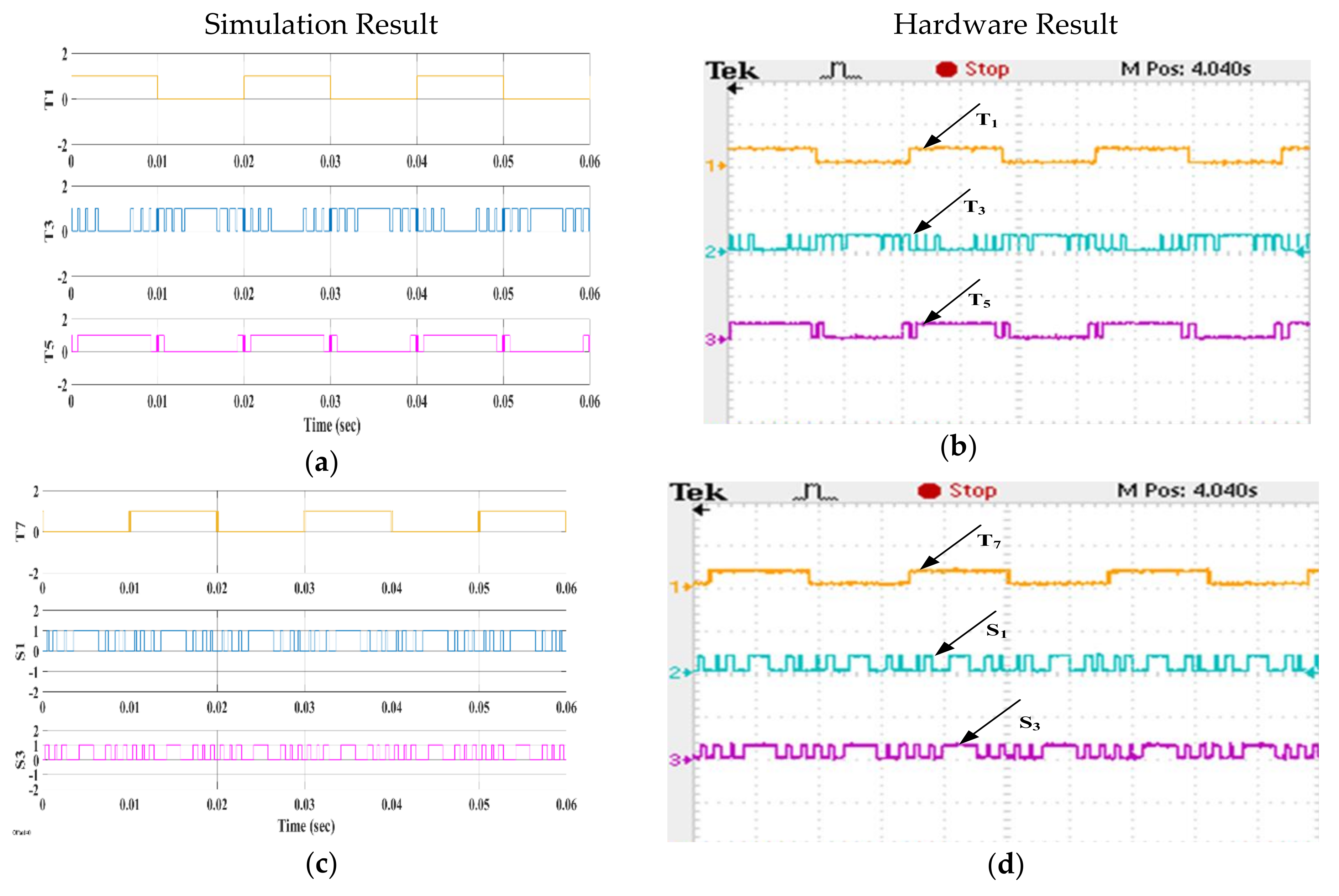
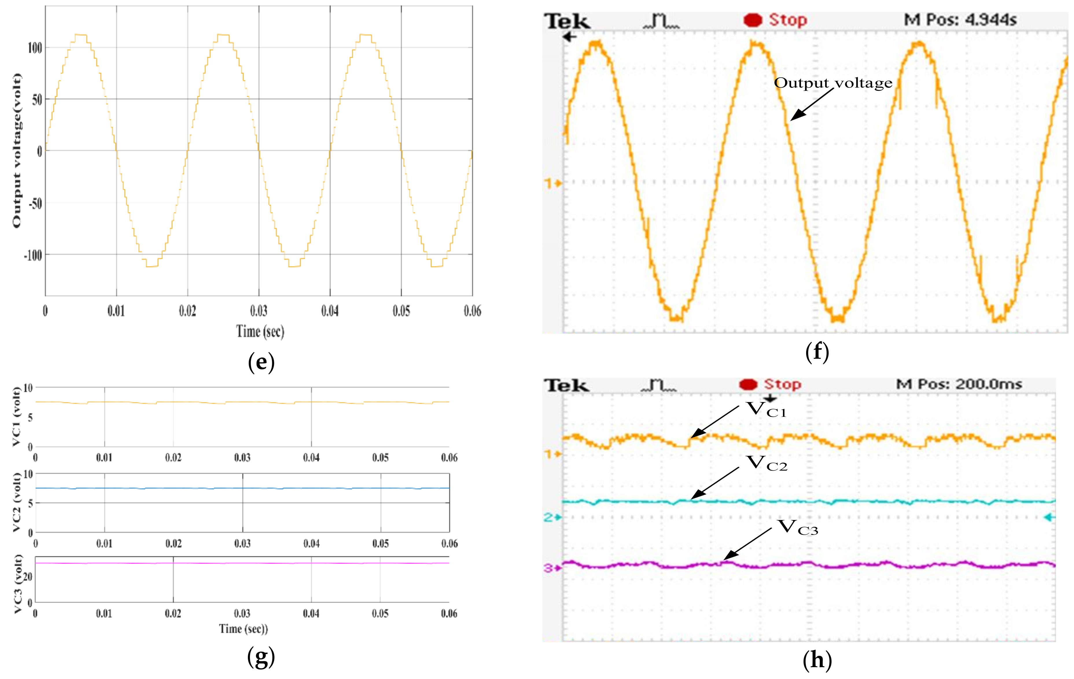
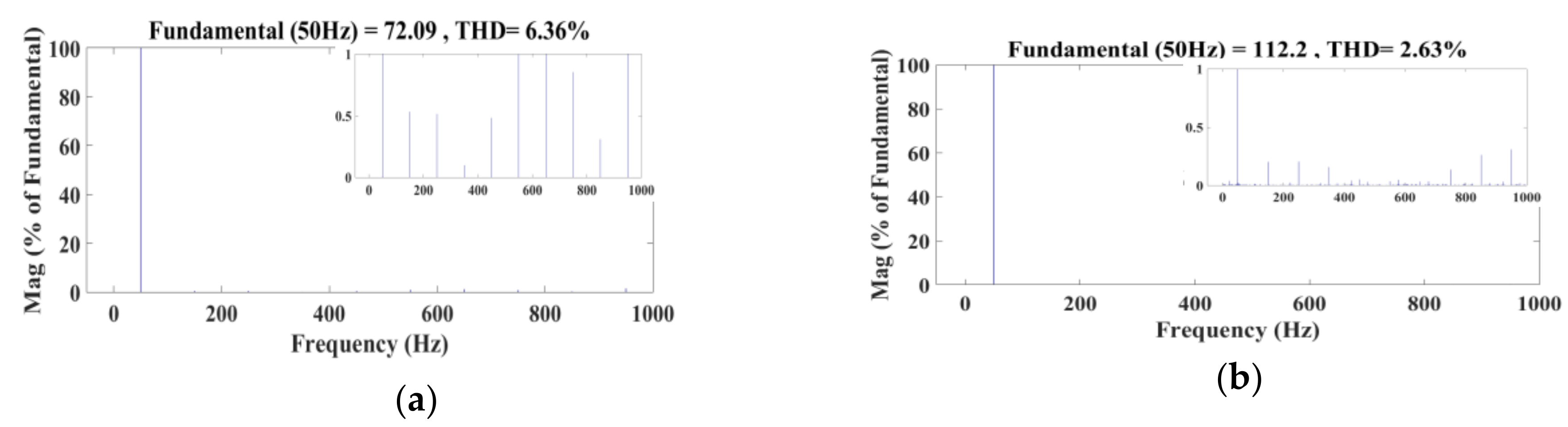
Section 7 presents simulation and hardware results, and the paper is concluded in
Section 8. The nearest level control modulation scheme (NLC), which comes under the fundamental switching frequency scheme [
26], is employed for controlling the switches.

 ,
, 


