Article

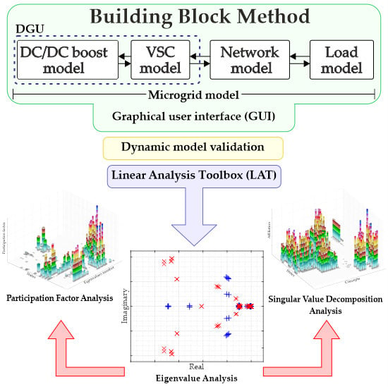
A Building Block Method for Modeling and Small-Signal Stability Analysis of the Autonomous Microgrid Operation

Department of Power Engineering, Faculty of Electronic Engineering, University of Niš, Aleksandra Medvedeva 14, 18115 Niš, Serbia
*
Author to whom correspondence should be addressed.
Energies 2020, 13(6), 1492; https://doi.org/10.3390/en13061492
Submission received: 19 February 2020 / Revised: 9 March 2020 / Accepted: 18 March 2020 / Published: 21 March 2020
(This article belongs to the Special Issue Dynamic Modeling of Microgrids)

Abstract

:
The task of the whole microgrid state-space matrix creation is usually done in a preferred textual programming language, and it presents a complicated, time-consuming, and error-prone job for a researcher without good coding practices. To ease the modeling task, contribute to the adaptation of new microgrid structures, control algorithms, and devices, and to improve the flexibility of the model, a graphical element building block method is proposed in this paper. With the proposed approach model creation of the whole microgrid is reduced to the creation of the individual element state-space model that is linked with other elements in a logical way with a graphical connection. Elements are then grouped into meaningful wholes and encapsulated with the appropriate graphical user interface that enables easy parameter modification and model complexity change. More detailed DC/DC and DC/AC models of converters than those in the literature concerning microgrid stability are presented in this paper. Those converters are incorporated in a microgrid, whose model is created using the proposed approach in MATLAB/Simulink. The dynamic response examination of the model remains easy, just as with all Simulink models, while for the linear system analysis, a specialized toolbox is used.

Graphical Abstract

1. Introduction

A large number of rural areas around the world require the use of Renewable Energy Sources (RESs) as the only solution for power supply. The autonomous microgrid imposes itself as an efficient and reliable solution in these conditions, where access to the main utility grid is unavailable or inefficient and costly. The electrification of such areas through a Low Voltage (LV) microgrid is achieved using the RESs as constitutive parts of distributive generation and Energy Storage Devices (ESDs). Compared to the main utility grid, the autonomous microgrid, due to the use of power converters as integrating devices for RESs and ESDs and the lack of synchronous generators, has low system inertia. The low system inertia, unpredictable nature of RESs, and fluctuations in consumption may cause frequency and voltage deviations, poor power-sharing ability among Distributed Generation Units (DGUs), and stability issues [1,2,3]. In the autonomous operation, microgrid should be able to remedy all these problems itself [4,5,6,7]. As the use of the RESs increase, the stability and control of microgrids have been a topic of great interest over various studies. In [8,9,10], the classification of microgrid stability is divided onto small-signal and transient stability.
The small-signal stability analysis, related to small-signal perturbation, is usually used to investigate the interaction effects between the DGUs and consumption in the defined steady-state operating point of the system. A different complexity of the microgrid models for small-signal analysis can be summarised as a detailed model, reduced model, and dynamic phasor model approach. Stability analysis based on eigenvalues derived from the detailed state-space model of the droop controlled microgrid is introduced in [11,12,13]. The problem of the stability related to the droop coefficient scheduling in a complex microgrid is considered in [14]. Further improvements of the microgrid model include the addition of control structures like the Phase-Locked Loop (PLL) model presented in [15] and the internal-model based controllers in [16] or microgrid elements such as DC/DC boost converter and ESD models given in [17,18]. The detailed microgrid model with secondary control included becomes even more complicated for modeling, as shown in [19,20], where the procedure for small-signal analysis is described. An idea of microgrid modeling with fewer variables, parameters, and equations is introduced in the form of a reduced system model in [21,22,23]. Despite a proper matching of the reduced order-model to the original in transients and steady-state operation point, a study [24] reveals that the stability analysis in the case of short circuit events provides unsatisfactory results. This study indicates the need for a new methodology for dominant eigenvalues selection and system reduction. An application of the dynamic-phasor modeling approach for the droop-controlled converters is presented in [25,26,27]. The stability analysis limitation imposed by the dynamic-phasor and reduced-order model compared to the detailed small-signal model in the case of the multi DGUs microgrid is given in [28]. As expected, the detailed small-signal state-space model stability analysis has the highest accuracy and modeling complexity compared to the reduced-order and dynamic-phasor models.
New studies conducted on the multi DGUs microgrids in the previous several years take into consideration more detailed models of the DGUs than those presented in the papers cited above. Thus, the digital control system time delay is considered in the state-space model of DGU in [29,30]. The model of the DGU considering the effects of dead-time and time delay on system stability in weak grids is analyzed in [31]. It is showed that the dead-time and time delay should not be neglected in microgrid modeling.
Recognizing the importance of the detailed modeling of microgrid elements, the trend of growing microgrid complexity, and the error-prone and rigid job of classical matrix-based modeling, the authors are herein proposing a graphical modeling approach. With the proposed approach, modeling of the whole microgrid state-space matrix is not required, instead the focus is on the modeling of individual elements. The whole model is obtained with a graphical connection of appropriate signals in MATLAB/Simulink R2018b (Update 6). In this way, overall linear models of microgrids and the accompanying structures are more comfortable to obtain. Several models of the same element can be provided and selected for analysis only with proper signal routing. Flexibility and robustness of the modeling are improved with encapsulation of the group of elements into meaningful wholes with a Graphical User Interface (GUI) that enables fast change of element model or parameters in model with a check-box or input field. For an analysis of a linear model, MATLAB/Simulink Linear Analysis Toolbox (LAT) is used. It provides various analysis tools for linear models and the ability to export obtained linear models into MATLAB workspace for further manipulation. The effectiveness of the proposed modeling approach is demonstrated in the case of the microgrid with DGUs where typical control structures are modeled, but also for the same microgrid where DGUs are modeled in more detail. Detail model accounts for power-electronics-based converter dead-time effect, the control of DC-link voltage via boost converter with appropriate control structures, and the effects that are related to digitally implemented control algorithm. In summary, the main benefits and key features of this paper are as follows:
  • The presented modeling approach provides higher flexibility through modularity, less chance for error through a better model overview, and easier microgrid analysis with tested toolboxes compared to traditional state-space matrix obtainment.
  • When models are created using the graphical building blocks method, elements in it are connected with other elements in the way to imitate the physical layout of the microgrid; thus, more natural modeling of the complex network configuration with different types of sources and loads is possible.
  • More detailed AC/DC and DC/DC converter models than those available in the literature are presented and analyzed as a direct benefit of the proposed modeling approach.
  • To support scientific collaboration and microgrid research, MATLAB/Simulink models from this paper, with accompanying documentation, are published on this paper’s MDPI webpage.
The rest of this paper is organized as follows: Section 2 gives the detailed linearized state-space models of each element of the microgrid. In Section 3, the proposed modeling approach is described along with the elements’ implementation procedure in the Simulink. In the first part of Section 4, a comparison between the linearized model and the model built using the Simscape toolbox is presented in terms of dynamic response. In the second part of Section 4, eigenvalue analysis is conducted on the linear model built using the proposed approach, followed by the participation factor and the singular value decomposition analysis.

2. Autonomous Microgrid Small-Signal State-Space Modeling

The autonomous LV microgrid representation, including n-DGUs, k-nodes with the load in each node, and j-lines, is presented in Figure 1.
It is assumed in Figure 1 that the integration of the RESs in the microgrid is accomplished over DGUs composed of a DC/DC boost converter and a DC/AC Voltage Source Converter (VSC). The presumption is made for an operation regime in which all RESs have sufficient energy to supply the loads. To apply the building block method and perform small-signal stability analysis with LAT, an individual state-space models of each component in the microgrid needs to be modeled. Four subsystems with associated components are identified:
  • Boost converter subsystem (power model, voltage and current controllers, digital control emulator models);
  • VSC subsystem (VSC with LCL filter model, power controller with virtual impedance loop, voltage and current controllers, dead-time, digital control emulator models);
  • Network subsystem (a resistive/indictive nature of power lines);
  • Load mode subsystem (a resistive/inductive load model).

2.1. State-Space Model of the DC/DC Boost Converter Subsystem

In this paper, the boost converter regulates the DC-link voltage udc to a reference value. For a power input from RES, the voltage source is assumed. Figure 2 presents a complete block diagram of the boost converter with a cascaded proportional-integral (PI) voltage and current controllers and Digital Control Emulator (DCE) blocks.

2.1.1. DC/DC Boost Converter Power Model

The boost converter power model is shown in Figure 3 and includes an inductor (inductance Llb and resistance Rlb), DC-link capacitor (capacitance Cdc), the resistance of the switching device during its conduction Ronb, and the forward diode voltage drop UDb. It is represented as a combination of the turn-on and turn-off states [32].
Dynamic equations of input/output voltages and currents uinb, udc, iinb, idc that average one switching cycle can be written as in Equations (1) and (2), respectively [33].
d i i n b d t = d b L l b ( u i n b ( R l b + R o n b ) i i n b ) + 1 d b L l b ( u i n b R l b i i n b U D b u d c ) ,
d u d c d t = d b C d c i d c + 1 d b C d c ( i i n b i d c ) .
In Equations (1) and (2) the duty cycle of the boost converter is represented with db. Linearizing the average model described with Equations (1) and (2) around the operating point, the small-signal state-space model of the boost converter can be obtained as in Equation (3).
[ Δ i i n b · Δ u d c · ] = [ ( R l b + D b R o n b ) L l b 1 D b L l b 1 D b C d c 0 ] A b [ Δ i i n b Δ u d c ] + [ 1 L l b 0 ] B 1 b [ Δ u i n b ] + [ U d c + U D b R o n b I i n b L l b I i n b C d c ] B 2 b [ Δ d b ] + [ 0 1 C d c ] B 3 b [ Δ i d c ] .
In Equation (3), Db, Udc, and Iinb represent the steady-state duty cycle, output DC-link voltage, and input inductor current, respectively. A similar principle is applied throughout the paper, where the upper-case symbols after linearization stand for the operating point of the system.

2.1.2. Voltage and Current Controllers

The outer voltage and inner current control loops with PI controllers are introduced to control the DC-link voltage. The voltage controller output provides the reference to the boost inductor current controller i i n b * . It is described with the following set of equations:
d ϕ b d t = u d c * u d c ,
i i n b * = K i u b ϕ b + K p u b u d c * K p u b u d c .
Voltage error between the reference DC-link voltage u d c * and measured u d c voltage, in Equation (4) is denoted as ϕ ˙ b , while Equation (5) defines boost input current reference. The Kpub and Kiub coefficients are proportional and integral terms of the boost voltage controller. Linearization of Equations (4) and (5) provides the following small-signal state-space model of the voltage controller:
[ Δ ϕ ˙ b ] = [ 0 ] A U b [ Δ ϕ b ] + [ 1 ] B 1 U b [ Δ u d c * ] + [ 1 ] B 2 U b [ Δ u d c ] ,
[ Δ i i n b * ] = [ K i u b ] C 1 U b [ Δ ϕ b ] + [ K p u b ] D 1 U b [ Δ u d c * ] + [ K p u b ] D 2 U b [ Δ u d c ] .
The output of the inductor current controller is db, obtained according to the following set of algebraic equations:
d γ b d t = i i n b * i i n b ,
d b = K i c b γ b + K p u b i i n b * K p u b i i n b .
The inductor current error γ ˙ b between the reference input current i i n b * and the measured i i n b is presented in Equation (8), while Equation (9) defines the boost duty cycle d b . The Kpib and Kiib coefficients are proportional and integral terms of the boost current controller. By linearizing Equations (8) and (9) around the operating point, the small-signal state-space model of the current controller is obtained and presented in Equations (10) and (11) as:
[ Δ γ ˙ b ] = [ 0 ] A I b [ Δ γ b ] + [ 1 ] B 1 I b [ Δ i i n b * ] + [ 1 ] B 2 I b [ Δ i i n b ] ,
[ Δ d b ] = [ K i c b ] C 1 I b [ Δ γ b ] + [ K p c b ] D 1 I b [ Δ i i n b * ] + [ K p c b ] D 2 I b [ Δ i i n b ] .

2.1.3. Digital Control Emulator Model

The process of continuous-time analog signal conversion to a discrete-time signal is called sampling. It is defined with time and amplitude quantization characteristics. In contrast to time quantization, amplitude quantization does not preserve the system linearity and produces effects that cannot be treated using linear system analysis [34]. However, the time quantization of a digital system can be represented with a series connection of the ideal sampler, the Zero-Order Hold (ZOH) [35,36], and digital execution of the algorithm as a transport delay. Combination of sampling, ZOH, and digital execution will be called Digital Control Emulator (DCE) [37] with a transfer function:
G d c e ( s ) = e s T s 1 T s 1 e s T s s ,
where Ts is the equivalent sampling period delay, and Laplace complex variable is denoted with s. The Pade approximation of Equation (12), as presented in [38], is used for the creation of a linear state-space model. In the boost converter subsystem, the DCE transfer function is applied on all input signals of the current controller.

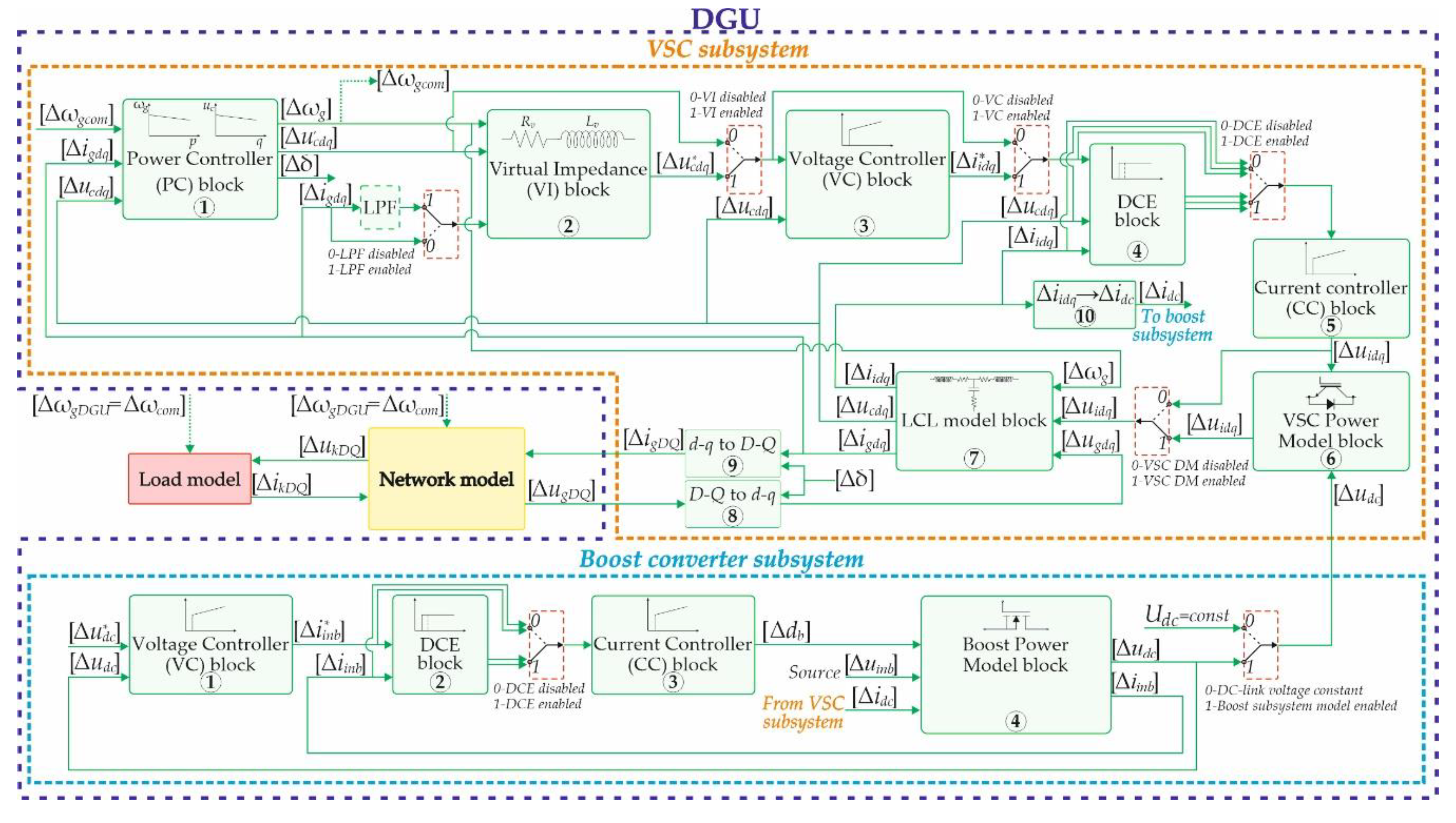
2.2. State-Space Model of the DC/AC Voltage Source Converter Subsystem

Figure 4 presents a block diagram of a single three-phase, three-wire, two-level VSC and its control structure connected to the grid through an LCL filter. Presented models in this subsection account for the effects induced by the switching frequency and the dead-time of the physical converter controlled by continuous space vector modulation technique, LCL filter used for its connection to the microgrid, power controller, cascaded PI voltage and current controllers, and DCE. Modeling will be done in the synchronous reference frame.

2.2.1. Reference Frame Transformation

In order to analyze the microgrid with several DGUs, the synchronous reference frame of one DGU is declared as a common reference frame (D-Q) with frequency ω g = ω g c o m , and all other individual inverters are transformed to this reference frame. The transformation of the grid voltage in the Point of Common Coupling (PCC) from the common to the individual reference frame of the VSC u g D Q u g d q and the transformation of the individual VSC output current to the common reference frame i g d q i g D Q are needed. These transformations are widely discussed in [12,13] and can be represented as:
[ Δ u g d Δ u g q ] = [ cos ( δ 0 ) sin ( δ 0 ) sin ( δ 0 ) cos ( δ 0 ) ] [ Δ u g D Δ u g Q ] + [ U g D sin ( δ 0 ) + U g Q cos ( δ 0 ) U g D cos ( δ 0 ) U g Q sin ( δ 0 ) ] [ Δ δ ] ,
[ Δ i g D Δ i g Q ] = [ cos ( δ 0 ) sin ( δ 0 ) sin ( δ 0 ) cos ( δ 0 ) ] [ Δ i g d Δ i g q ] + [ I g d sin ( δ 0 ) I g q cos ( δ 0 ) I g d cos ( δ 0 ) I g q sin ( δ 0 ) ] [ Δ δ ] ,
where Δ δ is a small phase angle difference between the reference frame in discussion and the common reference frame. The steady-state phase angle difference is denoted with δ 0 .

2.2.2. Power Controller

A complete block diagram of a power controller is given in Figure 5. It consists of a block for power calculation, a first-order Low-Pass Filter (LPF), and the frequency and voltage reference calculation blocks.
The instantaneous active p and reactive power q are calculated in the d-q reference frame, after amplitude-invariant Park’s transformation using the capacitor voltage uc and the grid current ig as in [15]. LPF with a cutoff frequency ωc is used to obtain filtered active and reactive power P and Q corresponding to the fundamental component.
The applicability of the conventional P-ω/Q-V droop control method in microgrids with dominant active resistance is confirmed in [39]. The nominal voltage and frequency values are set within the P-ω/Q-V droop control strategy according to the following equations:
ω g = ω n m p P δ = ( ω g ω g c o m ) d t ,
u c d = U n d n q Q ,
u c q = 0 .
where ωn, ωg, and ωgcom are frequencies during ideal no-load operation, when DGU is loaded with active power P, and the frequency of common reference frame, respectively. Und is the d voltage component setpoint and u c d , u c q are the output voltage d-q components when DGU is providing reactive power Q. The static droop gains for active power mp and reactive power nq are defined individually for every DGU according to its power capacity, allowed operating frequency range, and voltage deviation in the microgrid.
The small-signal model of the P-ω/Q-V controller in a state-space form is given in [15,16] as:
[ Δ δ ˙ Δ P ˙ Δ Q ˙ ] = [ 0 m p 0 0 ω c 0 0 0 ω c ] A p c [ Δ δ Δ P Δ Q ] + 3 2 ω c [ 0 0 0 0 I g d I g q U c d U c q I g q I g d U c q U c d ] B 1 p c [ Δ u c d Δ u c q Δ i g d Δ i g q ] + [ 1 0 0 ] B 2 p c [ Δ ω g ] ,
[ Δ ω g Δ u c d Δ u c q ] = [ 0 m p 0 0 0 n q 0 0 0 ] C p c [ Δ δ Δ P Δ Q ] .

2.2.3. Virtual Impedance

According to [39], a virtual resistance is introduced to eliminate the mismatch of DGU’s feeder line resistance and improve the power-sharing performances of DGU’s. In this paper, complex virtual impedance is used because of the real resistive/inductive nature of the lines. Figure 6 represents the equivalent block diagram of the virtual impedance algebraic approximation. To generate reference voltage components u c d * and u c q * an additional feedback loop to the droop output command voltages u c d and u c q is added. This loop consists of LPF and virtual impedance Z v = R v + j ω g L v , where R v and L v is virtual resistance and inductance, respectively.
To reduce the noise amplification, direct use of the virtual impedance algebraic approximation is avoided by adding the grid current filtering stage using LPF, as explained in [40]. The filtered grid current components i g d q f are used in the virtual impedance loop with dynamic representation:
d i g d f d t = ω c ( i g d i g d f ) ,
d i g q f d t = ω c ( i g q i g q f ) .
The voltage controller reference voltages u c d * and u c q * are generated as:
u c d * = u c d R v i g d f + L v ω g i g q f ,
u c q * = u c q R v i g q f L v ω g i g d f .
A linearized small-signal state-space model of virtual impedance with LPF based on Equations (20)–(23) can be derived as:
[ Δ i ˙ g d f Δ i ˙ g q f ] = [ ω c 0 0 ω c ] A v i r [ Δ i g d f Δ i g q f ] + [ ω c 0 0 ω c ] B 1 v i r [ Δ i g d Δ i g q ] ,
[ Δ u c d * Δ u c q * ] = [ R v L v Ω g L v Ω g R v ] C v i r [ Δ i g d f Δ i g q f ] + [ 1 0 0 1 ] D 1 v i r [ Δ u c d Δ u c q ] + [ L v I g q f L v I g d f ] D 2 v i r [ Δ ω g ] ,
where the nominal synchronous frequency is denoted as Ω g .

2.2.4. VSC Voltage and Current Controllers

The capacitor voltage and the converter inductance current controller realization is presented in Figure 7a,b, respectively. Controllers are implemented as standard PI with appropriate decoupling and capacitor voltage feed-forward terms as represented in Equations (27)–(28) and (32)–(33).
The measured capacitor voltages u c d q are subtracted from the reference voltage components u c d q * , and the obtained error is passed to the appropriate PI controller. The set of equations that describe the voltage controller are:
d ϕ d d t = u c d u c d d ϕ q d t = u c q u c q ,
i i d = K p u ( u c d u c d ) + K i u ϕ d ω g C f u c q ,
i i q = K p u ( u c q u c q ) + K i u ϕ q + ω g C f u c d ,
where Kpu and Kiu are proportional and integral gain of the voltage controller, respectively, while Cf represents the phase capacitance of the LCL filter.
The voltage controller linearized state-space model based on Equations (26)–(28), can be written in the small-signal form as:
[ Δ ϕ ˙ d Δ ϕ ˙ q ] = [ 0 0 0 0 ] A U v s c [ ϕ d ϕ q ] + [ 1 0 0 1 ] B 1 U v s c [ Δ u c d Δ u c q ] + [ 1 0 0 1 ] B 2 U v s c [ Δ u c d Δ u c q ] ,
[ Δ i i d * Δ i i q * ] = [ K i u 0 0 K i u ] C U v s c [ Δ ϕ d Δ ϕ q ] + [ K p u 0 0 K p u ] D 1 U v s c [ Δ u c d Δ u c q ] + [ K p u Ω g C f Ω g C f K p u ] D 2 U v s c [ Δ u c d Δ u c q ] .
The set of equations that describe the current controller are:
d ξ d d t = i i d i i d d ξ q d t = i i q i i q ,
u i d = K p i ( i i d i i d ) + K i i ξ d ω g L i i i q + u c d ,
u i q = K p i ( i i q i i q ) + K i i ξ q + ω g L i i i q + u c q ,
In Equations (32) and (33), Kpi and Kii present the proportional and integral current gain, respectively, while Li corresponds to the converter side inductor. With linearization of Equations (31)–(33), the state-space model for the current controller in the small-signal form is obtained as:
[ Δ ξ ˙ d Δ ξ ˙ q ] = [ 0 0 0 0 ] A I v s c [ ξ d ξ q ] + [ 1 0 0 1 ] B 1 I v s c [ Δ i i d Δ i i q ] + [ 1 0 0 1 ] B 2 I v s c [ Δ i i d Δ i i q ] ,
[ Δ u i d Δ u i q ] = [ K i i 0 0 K i i ] C I v s c [ Δ ξ d Δ ξ q ] + [ K p i 0 0 K p i ] D 1 I v s c [ Δ i i d Δ i i q ] + [ K p i Ω g L i Ω g L i K p i ] D 2 I v s c [ Δ i i d Δ i i q ] + [ 1 0 0 1 ] D 3 I v s c [ Δ u c d Δ u c q ] .

2.2.5. Three-Phase Two-Level Three-Wire VSC with Space Vector Modulation and LCL Filter

The link between the DC voltage of the VSC u d c and d-q components of the output voltage u i d and u i q can be established through the duty cycles dd and dq as:
u i d = d d u d c u i q = d q u d c .
Linearized small-signal state-space model of Equation (36) is given in Equation (37) as:
[ Δ u i d Δ u i q ] = [ D d D q ] [ Δ u d c ] + [ U d c 0 0 U d c ] [ Δ d d Δ d q ] .
The relation between the DC-link current idc and the d-q components of the VSC output current iid and iiq is achieved based on equality between the active power in DC-link pdc and active power at the output of the VSC p through:
p d c = p v d c i d c = 3 2 ( v i d i i d + v i q i i q ) i d c = 3 2 ( d d i i d + d q i i q ) .
Small-signal state-space model of Equation (38) is obtained with linearization around the operating point as:
[ Δ i d c ] = 3 2 [ D d D q ] [ Δ i i d Δ i i q ] + 3 2 [ I d I q ] [ Δ d d Δ d q ] .
Introduction of the dead-time model in VSC with continuous space vector modulation is presented in [31,41], where it was shown that dead-time creates a significant damping effect. Dead-time is modeled as a nonlinear function for d-q components of the VSC output current iid and iiq as:
f d t ( i i d , i i q ) = 1 L i T d t T s w 2 6 π [ i i d i i d 2 + i i q 2 u d c i i q i i d 2 + i i q 2 u d c ] ,
where T d t is the dead-time value, and T s w is the switching period.
The LCL filter attenuates the high-order harmonics originating from power switches of the converter. A model of the LCL filter in the d-q reference frame is presented in Figure 8.
Set of dynamic equations that account for the VSC dead-time effect when the combination of a continuous space vector modulation and the LCL filter is used, can be written as:
d i i d d t = r i L i i i d + ω g i i q + 1 L i u i d 1 L i T d t T s w 2 6 π i i d i i d 2 + i i q 2 u d c 1 L i u c d ,
d i i q d t = r i L i i i q ω g i i d + 1 L i u i q 1 L i T d t T s w 2 6 π i i q i i d 2 + i i q 2 u d c 1 L i u c q ,
d u c d d t = ω g u c q ω g r f i i q + ω g r f i g q + 1 C f i i d 1 C f i g d + r f ( d i i d d t d i g d d t ) ,
d u c q d t = ω g u c d + ω g r f i i d ω g r f i g d + 1 C f i i q 1 C f i g q + r f ( d i i q d t d i g q d t ) ,
d i g d d t = r g L g i g d + ω g i g q + 1 L g u c d 1 L g u g d ,
d i g q d t = r g L g i g q ω g i g d + 1 L g u c q 1 L g u g q .
Linearization of Equations (41)–(46) around the operating point gives the small-signal state-space model of the LCL-filter in the following form:
[ Δ x ˙ l c l ] = A l c l [ Δ x l c l ] + B 1 l c l [ Δ u i d Δ u i q ] + B 2 l c l [ Δ u g d Δ u g q ] + B 3 l c l [ Δ ω g ] ,
where: [ Δ x ˙ l c l ] = [ Δ i ˙ i d Δ i ˙ i q Δ i ˙ g d Δ i ˙ g q Δ u ˙ c d Δ u ˙ c q ] T , [ Δ x l c l ] = [ Δ i i d Δ i i q Δ i g d Δ i g q Δ u c d Δ u c q ] T ,
B 1 l c l = [ 1 L i 0 0 0 R f L i 0 0 1 L i 0 0 0 R f L i ] T , B 2 l c l = [ 0 0 1 L g 0 R f L g 0 0 0 0 1 L g 0 R f L g ] T ,
B 3 l c l = [ I i q I i d I g q I g d U c q U c d ] T ,
A l c l = [ R i L i K d t I i q 2 U d c Ω g + K d t I i d I i q U d c 0 0 1 L i 0 Ω g + K d t I i d I i q U d c R i L i K d t I i d 2 U d c 0 0 0 1 L i 0 0 R g L g Ω g 1 L g 0 0 0 Ω g R g L g 0 1 L g 1 C f R f R i L i R f K d t I i q 2 U d c R f K d t I i d I i q U d c R f R g L g 1 C f 0 R f ( 1 L i + 1 L g ) Ω g R f K d t I i d I i q U d c 1 C f R f R i L i R f K d t I i d 2 U d c 0 R f R g L g 1 C f Ω g R f ( 1 L i + 1 L g ) ] .

2.2.6. Digital Control Emulator for VSC

DCE in the VSC subsystem is approximated the same way as for boost converter presented in Section 2.1.2. Equation (14). In the VSC subsystem, on all signals relevant to the current controller (reference current, measured current, and measured capacitor voltage), appropriate DCE function is applied.

2.3. State-Space Model of the Equivalent Power Line Subsystem

In general, mixed inductive/resistive nature of power lines is assumed. The equivalent power line model between two nodes in the d-q system is presented in Figure 9a,b, respectively. In general, a set of dynamic equations that describe d-q components of the current in the jth line, between the two nodes x and k in Figure 9 could be described according to Equations (48) and (49).
d i l x k D d t = R l x k L l x k i l x k D + ω g c o m i l x k Q + 1 L l x k u x D 1 L l x k u k D ,
d i l x k Q d t = R l x k L l x k i l x k Q ω g c o m i l x k D + 1 L l x k u x Q 1 L l x k u k Q .
The linearized state-space model based on Equations (48) and (49) in the small-signal form is:
[ Δ i ˙ l x k D Δ i ˙ l x k Q ] = [ R l x k L l x k Ω g Ω g R l x k L l x k ] A j [ Δ i l x k D Δ i l x k Q ] + [ 1 L l x k 0 0 1 L l x k ] B 1 j [ Δ u x D Δ u x Q ] + [ 1 L l x k 0 0 1 L l x k ] B 2 j [ Δ u k D Δ u k Q ] + [ I x k Q I x k D ] B 3 j [ Δ ω g c o m ] .
A complete small-signal state-space model of the test network from Figure 1 can be derived based on Equation (50) as:
[ Δ i ˙ n e t D Q ] = A n e t [ Δ i n e t D Q ] + B 1 n e t [ Δ u n e t D Q ] + B 2 n e t [ Δ ω g c o m ] .
To define the voltage in each node of the network, a concept of the virtual resistor Rn is applied. A symbolic form of node voltages is given in [12,13,42] as follows:
[ Δ u n e t D Q ] = R n ( M c o n v [ Δ i c o n v D Q ] + M l o a d [ Δ i l o a d D Q ] + M n e t [ Δ i n e t D Q ] ) ,
where M c o n v , M l o a d and M n e t are mapping matrices of converters, loads, and lines according to [12].

2.4. State-Space Model of the Load Subsystem

It is assumed that the consumption in the microgrid can be represented through the RL load model. Dynamic equations that describe the RL load model at the kth node of the microgrid are:
d i l o a d k D d t = R l o a d k L l o a d k i l o a d k D + ω g c o m i l o a d k Q + 1 L l o a d k u k D ,
d i l o a d k Q d t = R l o a d k L l o a d k i l o a d k Q ω g c o m i l o a d k D + 1 L l o a d k u k Q ,
The single load model in the small-signal state-space form based on Equations (53) and (54) is:
[ Δ i ˙ l o a d k D Δ i ˙ l o a d k Q ] = [ R l o a d k L l o a d k Ω g Ω g R l o a d k L l o a d k ] A l o a d k [ Δ i l o a d k D Δ i l o a d k Q ] + [ 1 L l o a d k 0 0 1 L l o a d k ] B 1 l o a d k [ Δ u k D Δ u k Q ] + [ I l o a d k Q I l o a d k D ] B 2 l o a d k [ Δ ω g c o m ] .

3. Proposed Building Block Modeling Method

3.1. State-Space Model Creation

Analysis of a linear microgrid model in literature most commonly starts with the creation of the complete system state matrix Asys [12,13,15,16,17,18,19,20,42]:
[ Δ X ˙ i n v Δ i ˙ n e t Δ i ˙ l o a d ] = A s y s [ Δ X i n v Δ i n e t Δ i l o a d ] .
It includes and combines the state matrices of aggregated converters state matrix, network state matrix, and complete loads state matrix. The creation of element state-space model and state-space matrix aggregation is usually done in some textual programming language, like MATLAB, R, or Python. This creates a matrix assembly job that is not easy, let alone the eventual debugging.
Figure 10 shows the comparison between the VSC voltage controller matrix definition in the textual programing language and the proposed graphical approach. On this level, the proposed approach provides no clear advantage; someone might argue that the lack of coding is the advantage; others might say that the code is easier to read. An additional benefit of the graphical approach is the fact that along with the state-space matrix definition, presented in Figure 10a,b, the complete state-space model of the voltage controller is created.
The advantage of the proposed approach can be seen in Figure 11. Here the comparison is made on the example of converter matrix creation. For a researcher inexperienced with matrix manipulation, the creation of a converter matrix in terms of matrix dimension fitting and debugging is a daunting task. Furthermore, if poor coding practices are applied, modification of the existing model can be a slow and error-prone process. The building block method showed in Figure 11b enables:
  • The converter matrix creation only with an appropriate connection of consisted elements, in a physically logical way. It allows the complex system modeling through the creation of individual control and power stage blocks, and their appropriate graphical connection to form the models of the microgrid subsystems.
  • The easy debugging procedure, since the inspection of the variable of interest requires an only connection with a scope, as in any MATLAB/Simulink simulation. Greater clarity and monitoring of the model input/output signals in the blocks reduce the possibility of modeling errors.
  • The easy modification of the desired element and with it model complexity. Greater flexibility and modularity of the system modeling is allowed, and also the spent time is significantly reduced. It is possible to easily remove, modify, or insert new blocks of different complexity in a model.
The previously presented voltage controller element is created in the same manner as the other elements presented in Section 2, using the building principle showed in Figure 12. Standard MATLAB/Simulink “Gain”, “Integrator”, and “Add” blocks present the foundation for the proposed modeling. All blocks are adopted for vector operations, enabling the creation of state-space matrices that mimic the matrices created in textual languages. The input of the required integrator is a vector sum of state signals multiplied by matrix A, and the input signals multiplied by matrix B. Signals at the integrator output represent element states. They are fed back to matrix A and forward into matrix C. At last, the input vector is multiplied with state-matrix D and summed with the output of state-matrix C in order to obtain desired output signals.

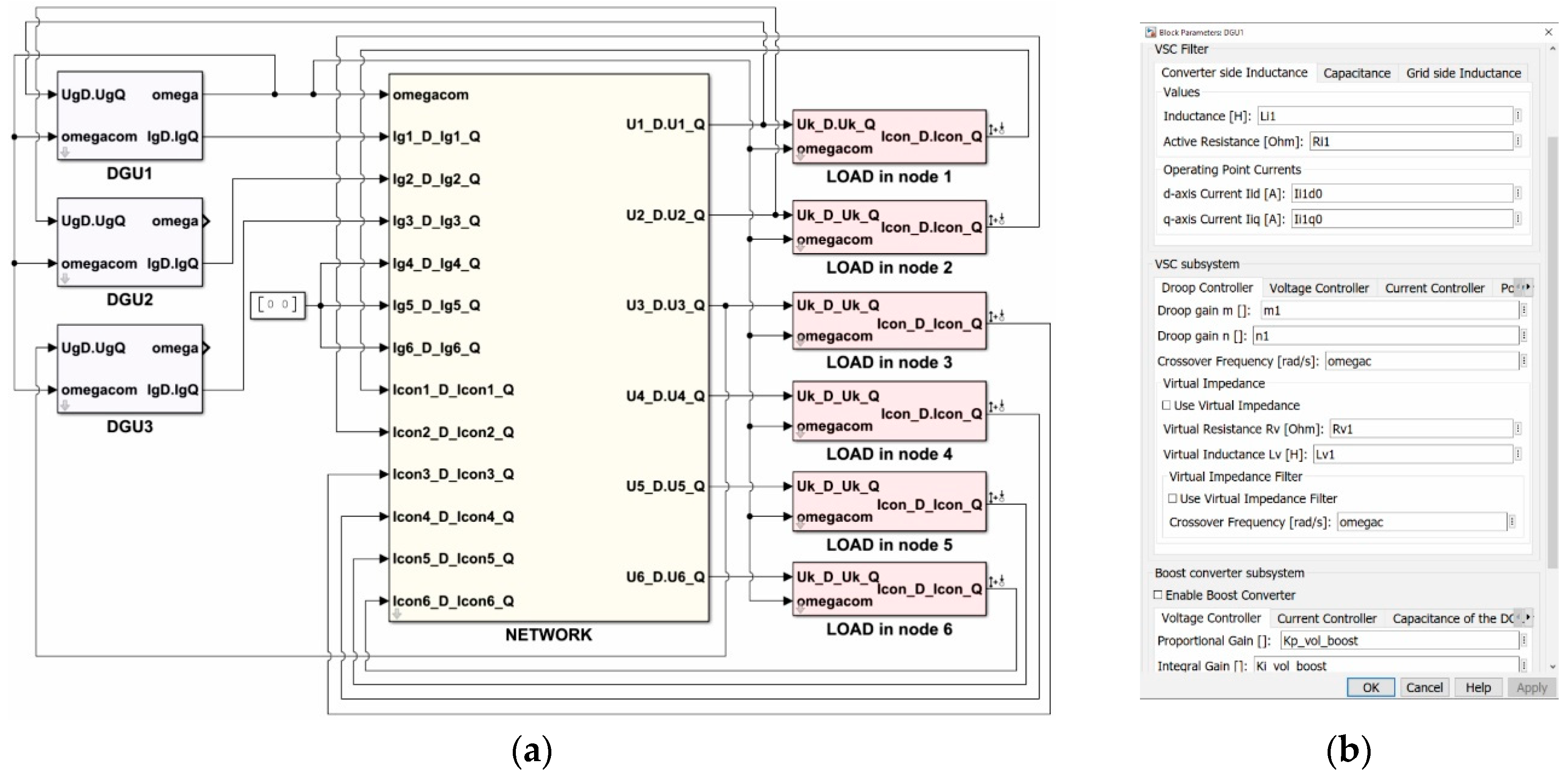
3.2. The Overview of the DGU Model

The overview of the individual DGU model with available state-space elements is given in Figure 13. All blocks in one DGU belong to one of two unities: VSC or Boost converter. In the same figure, all signals are represented as small-signal variations around the linearization point. In the case of small-signal analysis, this is true. When microgrid time-domain simulation for dynamic response examination is wanted, all signals correspond to actual values that can be expected. Also, for dynamic response test, power calculation block and reference frame calculation blocks are implemented as nonlinear equations.

3.2.1. Boost Converter Subsystem

The boost converter subsystem, according to Figure 13, consists of four building blocks and two selectors. The selector application allows easy enabling or disabling of an individual block of the model in the analysis. A voltage controller block ① in the boost subsystem is based on Equations (6) and (7), with the reference voltage Δ u d c * as input and measured DC-Link voltage Δ u d c as feedback into the block. The output of the block in the form of the reference current Δ i i n b * is forwarded together with the measured current Δ i i n b to DCE block ②. This block represents a unified model of the ideal sampler, zero-order hold and computational time delay models. Right after the digital control emulator block, a selector is implemented in order to enable or disable its usage in the boost subsystem model. To implement this block, a state-space representation of Equation (12) is needed. An application of MATLAB pade function for linear approximation and appropriate functions for state-space conversion creates matrices Adce, Bdce, Cdce, and Ddce that model DCE [43]. The next building block in the boost subsystem model, according to Figure 13, is the current controller block ③ modeled based on Equations (10) and (11). The boost duty cycle reference Δ d b as output from the current controller block is together with the source voltage Δ u i n b and DC-link current Δ i d c forwarded to the block that models physical boost converter ④. The boost converter model block is formed based on the state-space Equation (3). Its outputs are the DC-link voltage Δ u d c and inductor current Δ i d c , which are used as feedback to the model. A selector next to this block gives a possibility to work with constant voltage Δ u d c by disabling the boost subsystem model from DGU or enabling it by forwarding the voltage Δ u d c to the VSC subsystem model. Based on the state of this selector, a boost subsystem model may or may not be included in the analysis.

3.2.2. VSC Subsystem

A complete small-signal state-space model of the VSC subsystem in Figure 13 is composed of ten building blocks and four selectors. The building block ① represents the power controller model based on the state-space Equations (18) and (19). The inputs to the block are d-q components of the grid current Δ i g d q , capacitor voltage Δ u c d q , and frequency of the common reference frame Δ ω g c o m . Its outputs are capacitor reference voltage Δ u c d q , its reference frame frequency Δ ω g , and phase angle difference Δδ compared to the common reference frame; the first two of which are being forwarded to the virtual impedance block as inputs and third to the blocks ⑧ and ⑨. The virtual impedance block ② is modeled according to Equations (24) and (25), therefore the LPF and selector are placed between blocks ① and ②. The selector here enables or disables the LPF in the virtual impedance block model, so the grid current Δ i g d q filtering possibility exists. Another selector is used next to the virtual impedance block to enable or disable its usage in the VSC subsystem model. The next in line is the voltage controller block ③ with its input of capacitor voltage reference Δ u c d q * and feedback of measured Δ u c d q . A voltage controller block is implemented according to Equations (29) and (30) with the converter current reference Δ i i d q * as output. A selector next to block ③ is used to enable or disable a voltage regulation in the model. Same as in the boost subsystem, the DCE block ④ together with a selector is used in the VSC subsystem model. A current controller block ⑤ provides a reference for the converter output voltage Δ u i d q . This block is modeled according to Equations (34) and (35). Depending on the selector state, a reference Δ u i d q could be forwarded to the power model of the converter block ⑥ or the LCL filter model block ⑦. The power model of the converter is based on Equation (37) and represents the link with the boost converter subsystem taking a DC-link voltage as input Δ u d c . The LCL filter model block is modeled according to Equation (47) and links the DGU to the network model through blocks ⑧ and ⑨. Blocks ⑧ and ⑨, according to Equations (13) and (14), transform a grid voltage from an individual DGU reference frame to the common reference frame and grid current from a common reference frame to an individual DGU reference frame, respectively. The link between the VSC output current Δiidq and the DC link current Δ i d c is made with block ⑩ according to Equation (39).

3.3. Network Subsystem

The small-signal state-space model of the whole network subsystem is represented in one block. The model is created according to the desired microgrid network topology, using Equations (51) and (52). The network subsystem is represented in Figure 14. The input of the network block is the state vector, which consists of the converter’s grid current subvector Δ i c o n v D Q , load’s current subvector Δ i l o a d D Q , and frequency of the common reference frame Δ ω g c o m . The output of the block is a node voltage vector Δ u n e t D Q .

3.4. Load Subsystem

The block model of the individual load at the kth node is formed according to the small-signal state-space Equation (55), and it is presented in Figure 15. The inputs of the block are voltage Δ u k D Q in the kth node of the network and frequency of the common reference frame Δ ω g c o m , while the output is the kth node load current Δ i l o a d k D Q .

3.5. A Complete Microgrid Model

The example of test microgrid from Figure 1 created using the building blocks method in MATLAB/Simulink environment is presented in Figure 16a. The provided GUI for each masked subsection (DGU, network, load) enables:
  • Fast parameter and control structure change, as can be seen from the example of DGU1 showed in Figure 16b.
  • An easy selection of the elements and control structure blocks that should be included in the analysis. Model scalability is achieved through the simple selection of the desired elements.
  • The switch between the dynamic model and linear model by a simple selection in the GUI. The dynamic model can be compared to the model made of SimPowerSystem components.
In this microgrid example, the frequency of the DGU1 is selected to be the common frequency of the microgrid system Δ ω D G U 1 = Δ ω c o m , and all other DGUs are translated to its reference frame.

3.6. Procedure for Small-Signal Model Analysis

As shown in Figure 16, provided the Simulink state-space model of the microgrid is encapsulated in appropriate blocks, each of them with appropriate GUI. Using the LAT, it is possible to perform a stability analysis of the whole system or its individual blocks in a simple way. By defining (selecting) of the input and output signals at the points of interest in the model, the desired analysis of the corresponding block is performed. The LAT gives different possibilities for stability analysis (pole-zero placement, Bode plot, Nyquist plot, Nichols plot). If the output currents signal of all load blocks is selected, one by one, using right-click and if the option “Linear Analysis–Complementary Sensitivity” is selected, LAT will be instructed to compute the closed-loop transfer function backward from those selected outputs. To ensure that all states are accounted for, common frequency should be selected as “Input Perturbation” with the previously described procedure. By navigating through tab “Analysis” in the Simulink window, then “Control Design—Linear Analysis…”, the LAT window will open. The overview of LAT with the example pole-zero map for the microgrid model presented in this paper is shown in Figure 17. In the “SETUP” section of the “LINEAR ANALYSIS” tab, an inspection of the model’s inputs and outputs, model linearization at the arbitrarily operating point, and parameter variation can be done. The last one mentioned is of interest in the case of the inspection of how a variation of parameter, or a linear combination of parameters, influence the system. For the microgrid model pole-zero placement analysis in the complex plane, the option “Pole-Zero Map” should be selected from the “LINEARIZE” section of “LINEAR ANALYSIS” tab. Upon successful calculation of the model poles and zeros for the provided setup, a pole-zero map is provided in the main window and in “Linear Analysis Workspace” a state-space model of the microgrid is saved. If further manipulation of the state-space form model is required, it can be transferred to standard “MATLAB Workspace” by means of drag-and-drop. In the main window section, LAT will provide a graphical representation of the pole-zero map. With the mouse cursor hover over the pole or zero of interest, its precise location in the complex plane, damping ratio, overshoot, and frequency are shown.

4. Demonstration of the Applied Methodology

This section shows the results of typical tests that are used for the microgrid analysis. The validation of the proposed state-space model is done in MATLAB/Simulink R2018b (Update 6) on the test microgrid model presented in Figure 1 (simulation file MicrogridEnergiesFULL.slx using parameters from LiveScript MicrogridEnergiesParam.mlx). In Simulink configuration parameters, a variable step solver with the ode23tb method is selected. For a reference model, the microgrid is created using power elements from the Simscape toolbox (Simscape–Electrical–Specialized Power Systems–Fundamental Blocks), with the control structures implemented in a discrete domain. Inside the necessary “powergui” block continuous simulation type is selected. Details of two state-space models of the test microgrid shown in Figure 1 are presented in Table 1.
In the later analysis, here presented order of model elements, with the order of states presented in appropriate subsection will be assumed. For a linear approximation of the DCE model, 3rd order Pade approximation is used.
In the following subsections, first, the dynamic response of the models are compared in order to test their validity. After that, the participation factor analysis for both state-space models is provided, to determine what states contribute to the creation of a specific eigenvalue of interest. In the last part of this section, singular value decomposition analysis is used in order to gain an insight into groups of states that might share similar characteristics.

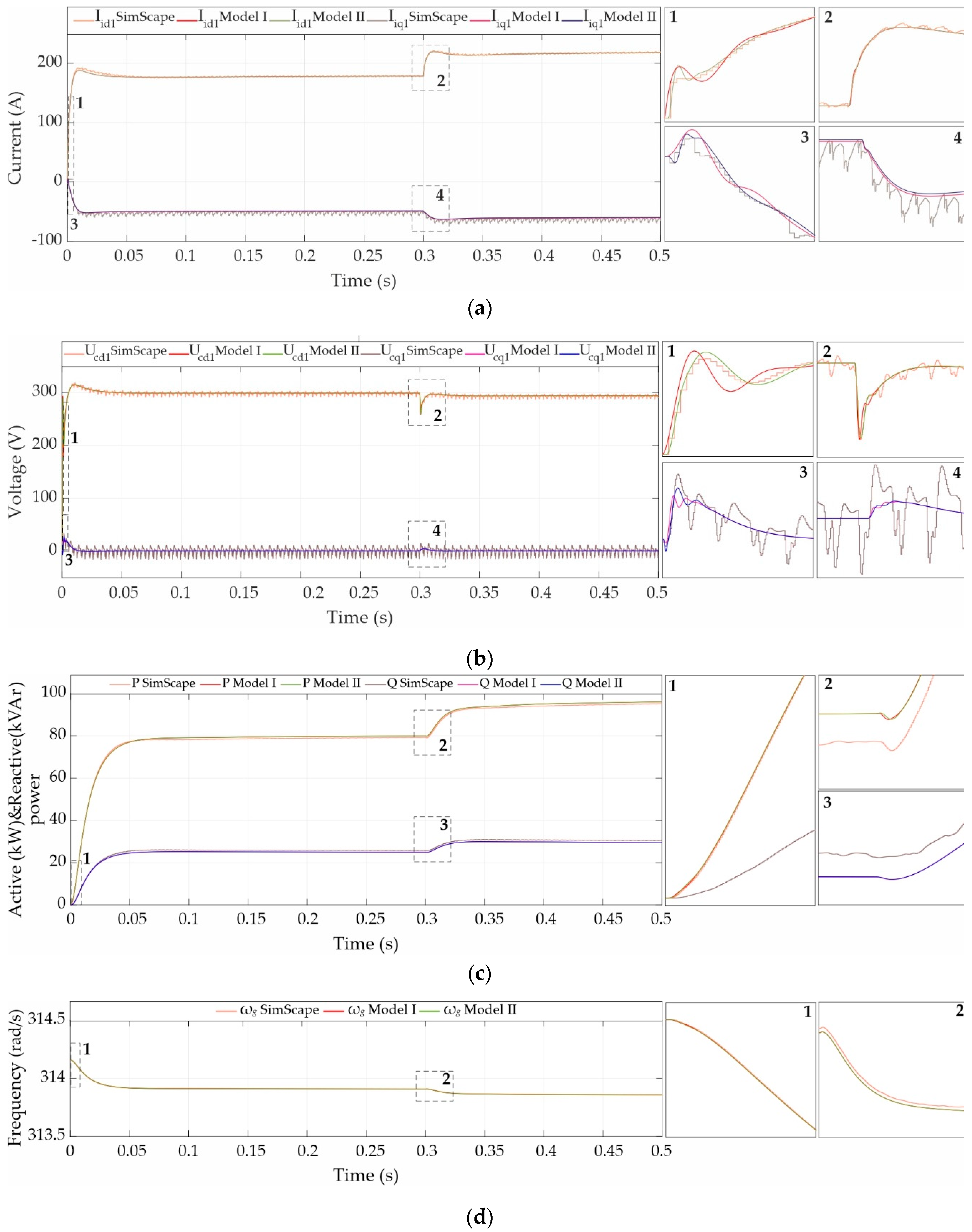
4.1. Building Block Model Validation

The accuracy of the proposed microgrid model developed in the state-space form and implemented in Simulink was compared with the model created in Simulink using SimPowerSystem Toolbox. The system parameters are presented in Table 2, and the steady-state operating point of each DGU is given in Table 3. The authors optioned for a steady-state operating point obtainment from the model built using SimPowerSystem, as used in [18]. The impedances of the microgrid lines in Table 2 are taken from the cable catalog data considering expected load flow, power losses, and voltage drop.
The comparison of the first DGU’s converter current, capacitor voltage, active and reactive power, and frequency is presented in Figure 18a–d, respectively. The presented time interval shows the start-up transient and the step load change at node 6 in 0.3 s (load at that node is doubled).
Comparison is made between the Simscape model, the microgrid model denoted as model I, and the microgrid model denoted as model II (defined in Table 1). From Figure 18a, a comparison of the presented models’ converter current response shows a small difference between models I and II at the start-up transient and the load change in terms of damping. The detailed model has higher damping in mentioned moments compared to the model I and with it, a higher resemblance to the waveform obtained using Simscape. The same can be spotted in Figure 18b with the comparison of capacitor voltage waveforms. As expected, during the steady-state operation, in all presented waveforms, there are no significant differences between the models I and II. As noted in Section 3.2, for dynamic response test, power calculation block and reference frame calculation blocks are implemented as nonlinear equations.

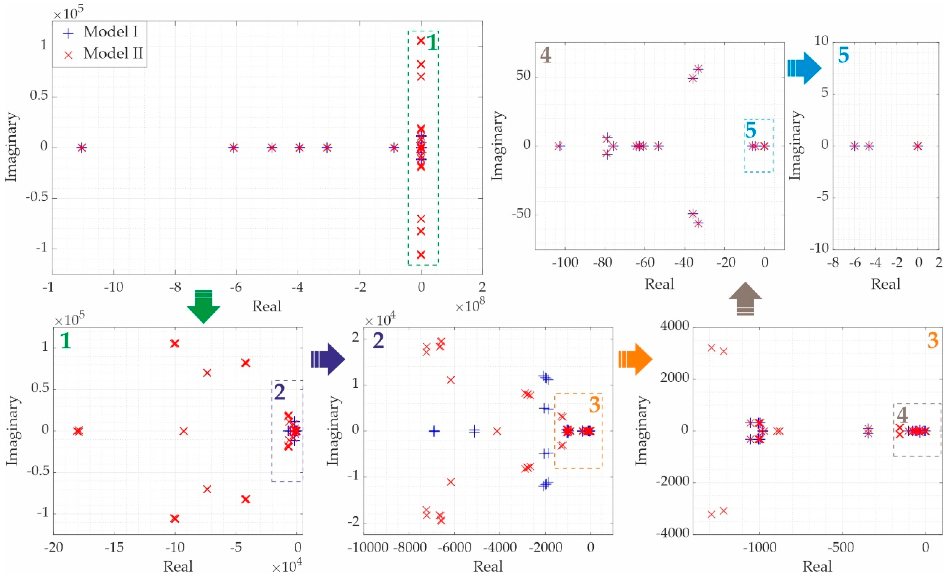
4.2. Eigenvalue Analysis Using LAT

Since in the complex plane the location of the model’s transfer function poles is equivalent to the location of the model’s state-space eigenvalues, the LAT tool can be directly used for eigenvalue analysis of the microgrid (done using MicrogridEnergiesSSM.slx with parameters from LiveScript MicrogridEnergiesParam.mlx). With the procedure described in Section 3.6 after the calculation of the microgrid model transfer function, the inbuild LAT tool can be used for pole (eigenvalue) obtainment.
The comparison of eigenvalue location of the model I and II for the parameters described in Table 2 and steady-state described in Table 3 is shown in Figure 19. Although it is noted that model I has 67 and model II has 247 states, due to the virtual impedance of the second DGU that is equal to zero, in all consequent analysis, two fewer states are shown (65 and 245). In the upper left part of Figure 19, the locations of all eigenvalues are shown. The boxed area denoted with 1 is presented in the lower-left part of Figure 19 and represents a zoomed-in part of the previous graph. The same principle is applied to all subsequent graphs.

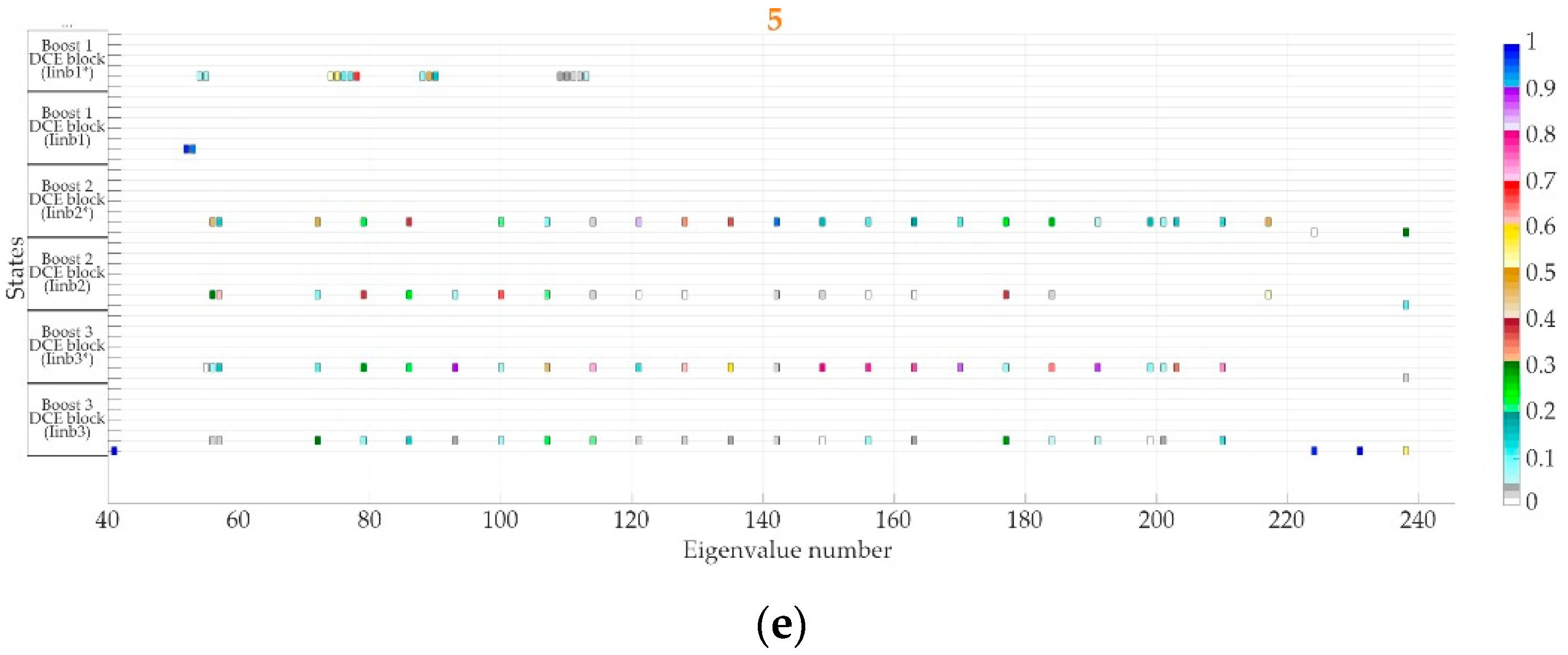
4.3. Participation Factor Analysis

In detail modeled microgrids, it is useful to quantify the contribution of each element of the state matrix to a specific eigenvalue. The usual mathematical tool for this quantization, called the participation factor, relies on the unique properties of left and right eigenvectors [44]. Participation factor obtainment cannot be done directly in LAT. Instead, a state-space model of the microgrid has to be exported to the MATLAB workspace where this additional analysis is conducted (done using MicrogridEnergiesPF.m file). Normalized participation of each state in every eigenvalue of the model I and II are presented in Figure 20a,b, respectively.
In Figure 20, the order of eigenvalue numeration is from the leftmost to the right. A pattern can be noticed in Figure 20a that the first state-space element of all Power Controllers (PCs) influences a wide number of eigenvalues. In general, its influence increases as the eigenvalues of interest are closer to the imaginary axis of the complex plane. Also, the influence of Virtual Impedance (VI) on some low-frequency eigenvalues can be noticed. Loads participate in the forming on the eigenvalues in the middle spectrum. For this selection of values, LCL filters have small importance, mostly on the medium-frequency eigenvalues. Voltage and current controllers (VC and CC, respectively) have an impact on the medium-frequency eigenvalues.
The participation factor analysis of the microgrid model II is shown in Figure 20b, mostly for demonstrative purposes. The detailed overview of the boxed sections of interest is shown in Appendix A. On this paper’s MDPI website supplementary material is published that includes presented figures built-in MATLAB for detailed inspection. What can be concluded is that DCE has a significant contribution to the forming of a large number of eigenvalues.

4.4. Singular Value Decomposition Analysis

Frequently used for compression and low-dimensional representation of high-dimensional matrices in data science, singular value decomposition (done using MicrogridEnergiesSVD.m file) is also a valuable tool for the analysis of ”belongings” or “concepts” hidden in the original matrix [45]. Namely, columns of left singular vectors can provide an insight into what state-space variables can be grouped under similar “concepts,” no matter how abstract that group might be. Values of the matrix that contain left singular vectors are graphically showed in Figure 21 for model I. The clustering of the matrix shows the first cluster that can be formed on concepts 1 to 12 and that it dominantly includes state-space variables of the microgrid network and DGU’s LCL filter models. The second cluster formed on concepts 13 to 18 groups state-space variables of all LCL filters. In addition to state-space variables of the first and the second, the third cluster of concepts (from 19 to 34) includes most of the state-space variables from power controllers. The third group (35 to 45) consists mainly of the load state-space variables. The next group (46 to 51) consists of current controller state-space variables, followed by the virtual impedance (52 to 56), voltage controllers with load model (57 to 62), and the rest of the state-space variables from the power controllers (63 to 65).

5. Conclusions

A building block modeling method based on MATLAB/Simulink is proposed in this paper. The main results can be considered from two aspects.
From the first aspect, the proposed method enables complex system modeling through the creation of individual block elements, and their appropriate graphical connection. In this way, a more flexible system modeling is achieved. Available elements complexity and control structures are easily changeable through GUI that encapsulates subsystems. The proposed method leverages the additional toolbox that enables fast linear system analysis.
From the second aspect, the detailed models of elements from the literature are synthesized and extended in this paper. As an illustration of the proposed building block method, two models are investigated. Typically considered elements for the microgrid modeling are grouped as the first model. The second model extends the first with an additional boost controller subsystem and digital control emulator. The dynamic response is used for these model validations, and it is shown that, of the tested models, the second model has a higher resemblance to the model build using Simscape. Participation factor analysis shows that the dynamic control emulator has a contribution to the creation of a high number of eigenvalues.
Future work will include expansion of the model capabilities in order to analyze hybrid microgrids, microgrids with rotating machines, and the effects of secondary control on the stability.

Supplementary Materials

The following are available online at https://www.mdpi.com/1996-1073/13/6/1492/s1, simulation files MicrogridEnergiesFULL.slx and MicrogridEnergiesSSM.slx, LiveScript file MicrogridEnergiesParam.mlx, and .m files MicrogridEnergiesPF.m and MicrogridEnergiesSVD.m.

Author Contributions

Conceptualization and writing—original draft, B.B.; Methodology, N.M.; Supervision, M.P.; Visualization, F.F. and V.K. All authors have read and agreed to the published version of the manuscript.

Funding

This research received no external funding.

Acknowledgments

This work has been supported by the Ministry of Education, Science and Technological Development of the Republic of Serbia.

Conflicts of Interest

The authors declare no conflict of interest.

Appendix A

The detailed overview of the boxed area presented in Figure 20b is shown in Figure A1.
Figure A1. Detailed representation of the boxed areas from Figure 20b: (a) boxed area 1, (b) boxed area 2, (c) boxed area 3, (d) boxed area 4, (e) boxed area 5.
Energies 13 01492 g0a1aEnergies 13 01492 g0a1b

References

  1. Hirsch, A.; Parag, Y.; Guerrero, J. Microgrids: A review of technologies, key drivers, and outstanding issues. Renew. Sustain. Energy Rev. 2018, 90, 402–411. [Google Scholar] [CrossRef]
  2. Gaur, P.; Singh, S. Investigations on Issues in Microgrids. J. Clean Energy Technol. 2017, 5, 47–51. [Google Scholar] [CrossRef] [Green Version]
  3. Badal, F.R.; Das, P.; Sarker, S.K.; Das, S.K. A survey on control issues in renewable energy integration and microgrid. Prot. Control Mod. Power Syst. 2019, 4, 8. [Google Scholar] [CrossRef] [Green Version]
  4. Parhizi, S.; Lotfi, H.; Khodaei, A.; Bahramirad, S. State of the art in research on microgrids: A review. IEEE Access 2015, 3, 890–925. [Google Scholar] [CrossRef]
  5. Brearley, B.J.; Prabu, R.R. A review on issues and approaches for microgrid protection. Renew. Sustain. Energy Rev. 2017, 67, 988–997. [Google Scholar] [CrossRef]
  6. Mahmoud, M.S.; Alyazidi, N.M. Pilot-Scale Implementation of Coordinated Control for Autonomous Microgrids. In Microgrid: Advanced Control Methods and Renewable Energy System Integration; Elsevier: Cambridge, MA, USA, 2017; pp. 341–367. ISBN 9780081012628. [Google Scholar]
  7. Du, W.; Lasseter, R.H.; Khalsa, A.S. Survivability of autonomous microgrid during overload events. IEEE Trans. Smart Grid 2019, 10, 3515–3524. [Google Scholar] [CrossRef]
  8. Shuai, Z.; Sun, Y.; Shen, Z.J.; Tian, W.; Tu, C.; Li, Y.; Yin, X. Microgrid stability: Classification and a review. Renew. Sustain. Energy Rev. 2016, 58, 167–179. [Google Scholar] [CrossRef]
  9. Farrokhabadi, M.; Canizares, C.A.; Simpson-Porco, J.W.; Nasr, E.; Fan, L.; Mendoza-Araya, P.; Tonkoski, R.; Tamrakar, U.; Hatziargyriou, N.D.; Lagos, D.; et al. Microgrid Stability Definitions, Analysis, and Examples. IEEE Trans. Power Syst. 2019, 35, 13–29. [Google Scholar] [CrossRef]
  10. Vadi, S.; Padmanaban, S.; Bayindir, R.; Blaabjerg, F.; Mihet-Popa, L. A review on optimization and control methods used to provide transient stability in microgrids. Energies 2019, 12, 3582. [Google Scholar] [CrossRef] [Green Version]
  11. Coelho, E.A.A.; Cortizo, P.C.; Garcia, P.F.D. Small-signal stability for parallel-connected inverters in stand-alone ac supply systems. IEEE Trans. Ind. Appl. 2002, 38, 533–542. [Google Scholar] [CrossRef]
  12. Pogaku, N.; Prodanović, M.; Green, T.C. Modeling, analysis and testing of autonomous operation of an inverter-based microgrid. IEEE Trans. Power Electron. 2007, 22, 613–625. [Google Scholar] [CrossRef] [Green Version]
  13. Yu, K.; Ai, Q.; Wang, S.; Ni, J.; Lv, T. Analysis and Optimization of Droop Controller for Microgrid System Based on Small-Signal Dynamic Model. IEEE Trans. Smart Grid 2016, 7, 695–705. [Google Scholar] [CrossRef]
  14. Díaz, G.; González-Morán, C.; Gómez-Aleixandre, J.; Diez, A. Scheduling of droop coefficients for frequency and voltage regulation in isolated microgrids. IEEE Trans. Power Syst. 2010, 25, 489–496. [Google Scholar] [CrossRef]
  15. Rasheduzzaman, M.; Mueller, J.A.; Kimball, J.W. An accurate small-signal model of inverter-dominated islanded microgrids using (dq) reference frame. IEEE J. Emerg. Sel. Top. Power Electron. 2014, 2, 1070–1080. [Google Scholar] [CrossRef]
  16. Leitner, S.; Yazdanian, M.; Mehrizi-Sani, A.; Muetze, A. Small-Signal Stability Analysis of an Inverter-Based Microgrid with Internal Model-Based Controllers. IEEE Trans. Smart Grid 2018, 9, 5393–5402. [Google Scholar] [CrossRef]
  17. Krismanto, A.; Mithulananthan, N.; Lee, K.Y. Comprehensive Modelling and Small Signal Stability Analysis of RES-based Microgrid. IFAC-Pap. 2015, 48, 282–287. [Google Scholar] [CrossRef]
  18. Tang, X.; Deng, W.; Qi, Z. Investigation of the dynamic stability of microgrid. IEEE Trans. Power Syst. 2014, 29, 698–706. [Google Scholar] [CrossRef]
  19. Mohammadi, F.D.; Vanashi, H.K.; Feliachi, A. State-Space Modeling, Analysis, and Distributed Secondary Frequency Control of Isolated Microgrids. IEEE Trans. Energy Convers. 2018, 33, 155–165. [Google Scholar] [CrossRef]
  20. Begum, M.; Li, L.; Zhu, J.; Li, Z. State-Space Modeling and Stability Analysis for Microgrids with Distributed Secondary Control. In Proceedings of the 2018 IEEE 27th International Symposium on Industrial Electronics (ISIE), Cairns, Australia, 13–15 June 2018; pp. 1201–1206. [Google Scholar]
  21. Wang, Y.; Lu, Z.; Min, Y.; Wang, Z. Small signal analysis of microgrid with multiple micro sources based on reduced order model in islanding operation. In Proceedings of the IEEE Power and Energy Society General Meeting, Detroit, MI, USA, 24–29 July 2011. [Google Scholar]
  22. Mariani, V.; Vasca, F.; Vásquez, J.C.; Guerrero, J.M. Model Order Reductions for Stability Analysis of Islanded Microgrids with Droop Control. IEEE Trans. Ind. Electron. 2015, 62, 4344–4354. [Google Scholar] [CrossRef] [Green Version]
  23. Rasheduzzaman, M.; Mueller, J.A.; Kimball, J.W. Reduced-order small-signal model of microgrid systems. IEEE Trans. Sustain. Energy 2015, 6, 1292–1305. [Google Scholar] [CrossRef]
  24. Taoufik, Q.; Quentin, C.; Li, C.; Xavier Guillaud, F.; Colas; François Gruson, X.K. WP3—Control and Operation of a Grid with 100 % Converter-Based Devices Deliverable 3.2: Local Control and Simulation Tools for Large Transmission Systems; Horizon 2020—LCE-6 project report; Project MIGRATE: Bayreuth, Germany, 2018. [Google Scholar]
  25. Wang, L.; Guo, X.Q.; Gu, H.R.; Wu, W.Y.; Guerrero, J.M. Precise modeling based on dynamic phasors for droop-controlled parallel-connected inverters. In Proceedings of the IEEE International Symposium on Industrial Electronics, Hangzhou, China, 28–31 May 2012; pp. 475–480. [Google Scholar]
  26. Mendoza-Araya, P.A.; Venkataramanan, G. Dynamic phasor models for AC Microgrids stability studies. In Proceedings of the 2014 IEEE Energy Conversion Congress and Exposition, ECCE, Pittsburgh, PA, USA, 14–18 September 2014; pp. 3363–3370. [Google Scholar]
  27. Mariani, V.; Vasca, F.; Guerrero, J.M. Dynamic-phasor-based nonlinear modelling of AC islanded microgrids under droop control. In Proceedings of the 2014 IEEE 11th International Multi-Conference on Systems, Signals and Devices, SSD, Castelldefels-Barcelona, Spain, 11–14 February 2014. [Google Scholar]
  28. Guo, X.; Lu, Z.; Wang, B.; Sun, X.; Wang, L.; Guerrero, J.M. Dynamic phasors-based modeling and stability analysis of droop-controlled inverters for microgrid applications. IEEE Trans. Smart Grid 2014, 5, 2980–2987. [Google Scholar] [CrossRef] [Green Version]
  29. Wang, Y.; Wang, X.; Blaabjerg, F.; Chen, Z. Harmonic instability assessment using state-space modeling and participation analysis in inverter-fed power systems. IEEE Trans. Ind. Electron. 2017, 64, 806–816. [Google Scholar] [CrossRef]
  30. Wang, R.; Sun, Q.; Ma, D.; Liu, Z. The Small-Signal Stability Analysis of the Droop-Controlled Converter in Electromagnetic Timescale. IEEE Trans. Sustain. Energy 2019, 10, 1459–1469. [Google Scholar] [CrossRef]
  31. Rodriguez-Cabero, A.; Prodanovic, M.; Roldan-Perez, J. Analysis of dynamic properties of VSCs connected to weak grids including the effects of dead time and time delays. IEEE Trans. Sustain. Energy 2019, 10, 1066–1075. [Google Scholar] [CrossRef]
  32. Modabbernia, M.R.; Sahab, A.R.; Mirzaee, M.T.; Ghorbany, K. The state space average model of boost switching regulator including all of the system uncertainties. Adv. Mater. Res. 2012, 403, 3476–3483. [Google Scholar] [CrossRef]
  33. Erickson, R.W.; Maksimović, D. Fundamentals of Power Electronics; Kluwer Academic: New York, NY, USA, 2001; pp. 15–27. ISBN 9780792372707. [Google Scholar]
  34. Corradini, L.; Maksimović, D.; Mattavelli, P.; Zane, R. Digital Control of High-Frequency Switched-Mode Power Converters; John Wiley & Sons: Hoboken, NJ, USA, 2015; pp. 51–70. ISBN 9781119025498. [Google Scholar]
  35. Franklin, G.F.; Powell, J.D.; Workman, M.L. Digital control of Dynamic Systems; Addison-Wesley: Menlo Park, CA, USA, 1998; pp. 155–180. ISBN 0201820544. [Google Scholar]
  36. Zhang, X. Modelling and Control of Power Inverters in Microgrids. Ph.D. Thesis, University of Liverpool, Liverpool, UK, 2012. [Google Scholar]
  37. Agorreta, J.L.; Borrega, M.; López, J.; Marroyo, L. Modeling and control of N-paralleled grid-connected inverters with LCL filter coupled due to grid impedance in PV plants. IEEE Trans. Power Electron. 2011, 26, 770–785. [Google Scholar] [CrossRef]
  38. Levine, W.S. Control System Fundamentals; CRC Press: Boca Raton, FL, USA, 2010; Chapter 5; pp. 2–32. ISBN 9781420073621. [Google Scholar]
  39. Hou, X.; Sun, Y.; Yuan, W.; Han, H.; Zhong, C.; Guerrero, J.M. Conventional P-ω/Q-V droop control in highly resistive line of low-voltage converter-based AC microgrid. Energies 2016, 9, 943. [Google Scholar] [CrossRef] [Green Version]
  40. Rodriguez-Cabero, A.; Roldan-Perez, J.; Prodanovic, M. Virtual Impedance Design Considerations for Virtual Synchronous Machines in Weak Grids. IEEE J. Emerg. Sel. Top. Power Electron. 2019. [Google Scholar] [CrossRef]
  41. Ahmed, S.; Shen, Z.; Mattavelli, P.; Boroyevich, D.; Karimi, K.J. Small-Signal Model of Voltage Source Inverter (VSI) and Voltage Source Converter (VSC) Considering the DeadTime Effect and Space Vector Modulation Types. IEEE Trans. Power Electron. 2017, 32, 4145–4156. [Google Scholar] [CrossRef]
  42. Wu, X.; Shen, C. Distributed Optimal Control for Stability Enhancement of Microgrids with Multiple Distributed Generators. IEEE Trans. Power Syst. 2017, 32, 4045–4059. [Google Scholar] [CrossRef]
  43. Xue, D.; Chen, Y. System Simulation Techniques with MATLAB and Simulink; John Wiley & Sons: Chichester, UK, 2013; pp. 278–280. ISBN 9781118694374. [Google Scholar]
  44. Pal, B.; Chaudhuri, B. Robust Control in Power Systems; Springer: New York, NY, USA, 2005; pp. 17–19. ISBN 9780387259499. [Google Scholar]
  45. Leskovec, J.; Rajaraman, A.; Ullman, J.D. Mining of Massive Datasets, 2nd ed.; Cambridge University Press: Cambridge, UK, 2014; pp. 418–422. ISBN 9781107077232. [Google Scholar]
Figure 1. A simplified schematic diagram of the general microgrid model.
Energies 13 01492 g001
Figure 2. A DC/DC boost converter complete block diagram.
Energies 13 01492 g002
Figure 3. A DC/DC boost converter power model representation: (a) Switch-on state; (b) Switch-off state.
Energies 13 01492 g003
Figure 4. A Voltage Source Converter (VSC) complete block diagram.
Energies 13 01492 g004
Figure 5. The power controller block diagram.
Energies 13 01492 g005
Figure 6. The virtual impedance algebraic block diagram.
Energies 13 01492 g006
Figure 7. VSC controller realization with decoupling: (a) Voltage controller; (b) Current controller.
Energies 13 01492 g007
Figure 8. LCL-filter equivalent circuit: (a) d-axis equivalent circuit; (b) q-axis equivalent circuit.
Energies 13 01492 g008
Figure 9. The jth line equivalent circuit: (a) d-axis equivalent circuit; (b) q-axis equivalent circuit.
Energies 13 01492 g009
Figure 10. Comparison between voltage controller matrix definition: (a) textual language; (b) using the building block method.
Energies 13 01492 g010
Figure 11. Part of the converter state-space matrix creation: (a) textual language; (b) using the proposed method.
Energies 13 01492 g011aEnergies 13 01492 g011b
Figure 12. The general approach for element creation: (a) The state-space representation of an element creation; (b) The general representation of the MIMO block used in an element modeling.
Energies 13 01492 g012
Figure 13. The overview of DGU with all optional elements.
Energies 13 01492 g013
Figure 14. The network subsystem block.
Energies 13 01492 g014
Figure 15. The individual load subsystem model block.
Energies 13 01492 g015
Figure 16. The complete Simulink model of the microgrid: (a) DGUs, network, and loads created using building blocks approach; (b) Front-end mask of the DGU1.
Energies 13 01492 g016
Figure 17. The overview of modal analysis using LAT.
Energies 13 01492 g017
Figure 18. Comparison of the dynamic response of the microgrid built using Simscape, model I, and model II (from Table 1) in the case of DGU in node 1: (a) converter current; (b) capacitor voltage; (c) active and reactive power and; (d) output frequency.
Energies 13 01492 g018
Figure 19. Eigenvalues location of the considered microgrid.
Energies 13 01492 g019
Figure 20. Participation factor analysis of the considered microgrid: (a) microgrid model I; (b) microgrid model II.
Energies 13 01492 g020
Figure 21. Singular value decomposition of the microgrid model I.
Energies 13 01492 g021
Table 1. The state-space microgrid models.
STATE-SPACE MICROGRID MODEL I (67 states)
BlocksSubsection in paperNumber of states
Load in nodes 1,2,3,4,5 and 62.412
Network2.310
LCL-filter without dead-time effect and VSC model2.2.5 *6 per DGU
Power controller2.2.23 per DGU
Virtual impedance with LPF2.2.32 per DGU
VSC current and voltage controllers2.2.44 per DGU
STATE-SPACE MICROGRID MODEL II (247 states)
Additional blocks to MODEL ISubsection in paperNumber of states
LCL-filter with dead-time effect and VSC model2.2.56 per DGU
Digital control emulator2.2.642 per DGU
Boost converter model2.1.12 per DGU
Boost current and voltage controllers2.1.22 per DGU
Digital control emulator of boost2.2.614 per DGU
* Can be obtained by setting Tdt = 0 in Equations (41) and (42)
Table 2. The system parameters.
DGU1 = DGU2 = DGU3
ParameterValue
Nominal active power Pn100 kW
Nominal phase grid voltage Vn230 V
Nominal grid frequency fg50 HZ
VSC parametersValueVSC parametersValue
Switching frequency fsw10 kHzPower coefficient mp3.14 × 10−6
Dead time Tdt2 μsPower coefficient nq9 × 10−4
Equivalent sampling frequency Ts0.5*100 μsLPF cut-off frequency ωc62.8 rad/s
Output voltage Vc230 VVC proportional gain Kpu0.2475
Filter inductance Li163 μHVC integral gain Kiu437.5
Filter resistance Ri3 mΩCC proportional gain Kpi1.4224
Filter capacitance Cf70 μFCC integral gain Kii1241.3
Filter damping resistor Rf0.21 ΩVirtual impedance Zvsc1(19.6 + j3.9) mΩ
Filter inductance Lg34 μHVirtual impedance Zvsc2(0 + j0) mΩ
Filter resistance Rg1 mΩVirtual impedance Zvsc3(38.7 + j7.8) mΩ
Virtual impedance LPF ωc62.8 rad/s
Boost parametersValueBoost parametersValue
DC-link voltage Vdc800 VSwitching resistance Ronb2 mΩ
DC-link capacitor Cdc10 mFDiode voltage drop VDb1.1 V
Input voltage Vinb540 VVC proportional gain Kpub11.869
Filter inductance Llb300 μHVC integral gain Kiub364.07
Filter resistance Rlb1 mΩCC proportional gain Kpib0.0011
Switching frequency fswb10 kHzCC integral gain Kiib1.3229
Grid parametersValueLoad parametersValue
Line impedance Zl14(0.1162 + j0.0233) ΩLoad impedance Zload1(7 + j2.198) Ω
Line impedance Zl25(0.1356 + j0.0271) ΩLoad impedance Zload2(14 + j4.396) Ω
Line impedance Zl36(0.0969 + j0.0194) ΩLoad impedance Zload3(4.85 + j1.445) Ω
Line impedance Zl45(0.0193 + j0.0091) ΩLoad impedance Zload4(2.4 + j0.7536) Ω
Line impedance Zl56(0.0231 + j0.011) ΩLoad impedance Zload5,6(1.6 + j0.5024) Ω
Table 3. The microgrid steady-state operating point.
Steady-state operating points (DGU1 = 1, DGU2 = 2, DGU3 = 3)
ParameterValueParameterValue
Iid1, Iid2, Iid3 [A][180, 177, 182]Ilb1,Ilb2 Ilb3 [A][148, 148, 148]
Iiq1, Iiq2, Iiq3 [A][−51, −45, −52]Db1, Db2, Db3[0.326, 0.326, 0.326]
Ucd1, Ucd2, Ucd3 [V][299, 304, 295]I14D, I14Q [A][141, −42]
Ucq1, Ucq2, Ucq3 [V][0.5, 0, 1]I25D, I25Q [A][156, −42]
Igd1, Igd2, Igd3 [A][179, 175, 181]I36D, I36Q [A][127, −40]
Igq1, Igq2, Igq3 [A][−57, −51, −58]I45D, I45Q [A][34.5, −11]
UgD1, UgD2, UgD3 [V][296, 302, 292]I56D, I56Q [A][32, −6]
UgQ1, UgQ2, UgQ3 [V][3, 3, 3]Iload1D, Iload1Q [A][39, −12]
δ01, δ02, δ03 [rad][0, −3.88 × 10⁻⁴, −3.3 × 10⁻³]Iload2D, Iload2Q [A][19.6, −6]
Dd1, Dd2, Dd3[0.375, 0.381, 0.37]Iload3D, Iload3Q [A][55, −16]
Dq1, Dq2, Dq3[0.017, 0.017, 0.017]Iload4D, Iload4Q [A][106, −31]
Udc1, Udc2, Udc3, [V][800, 800, 800]Iload5D, Iload5Q [A][159, −47]
Iload6D, Iload6Q [A][158, −47]

