An Impedance Network-Based Three Level Quasi Neutral Point Clamped Inverter with High Voltage Gain


 ,
,  ,
,  , and
, and
Abstract
:1. Introduction
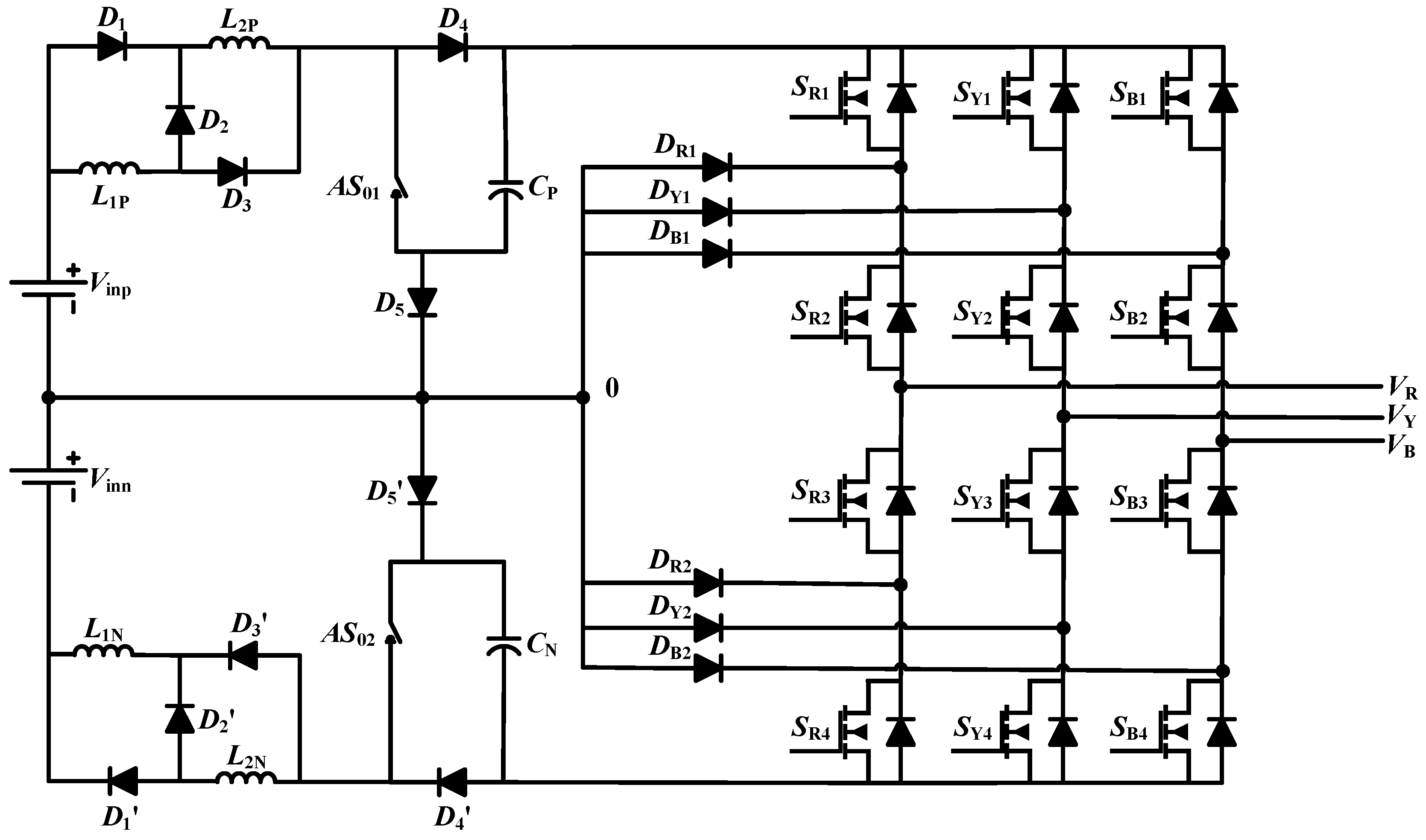
2. The Proposed Inverter Topology
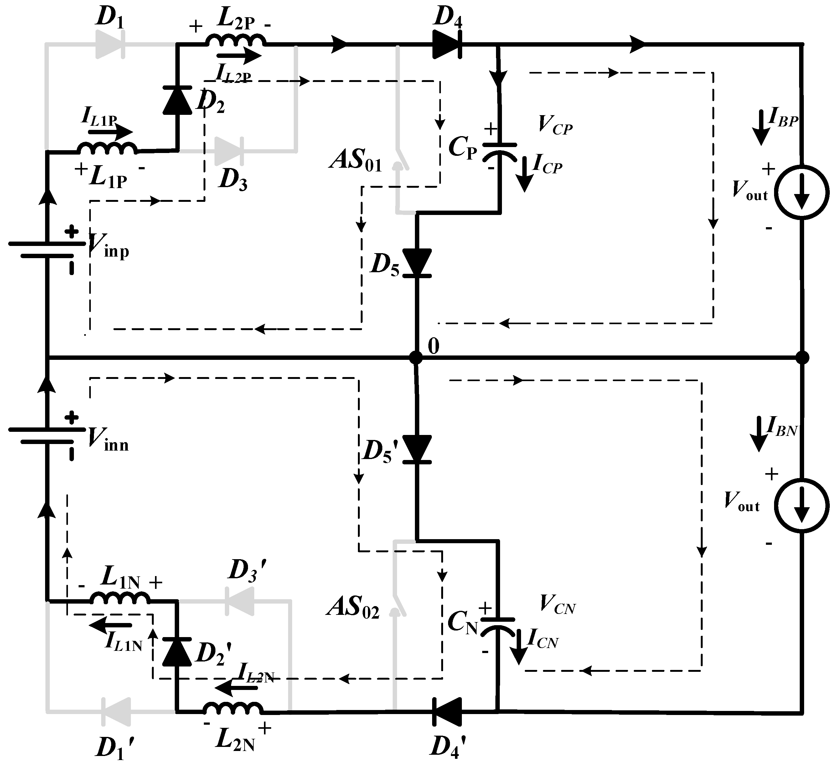
2.1. Active State
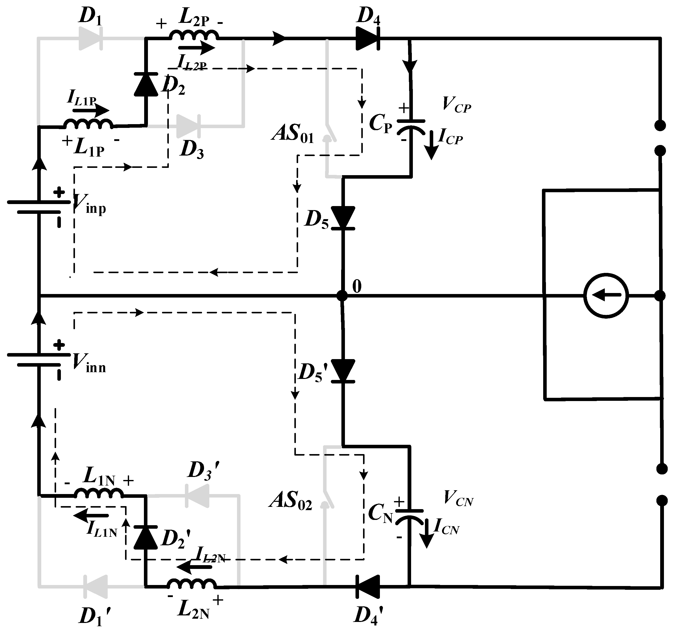
2.2. Zero-State
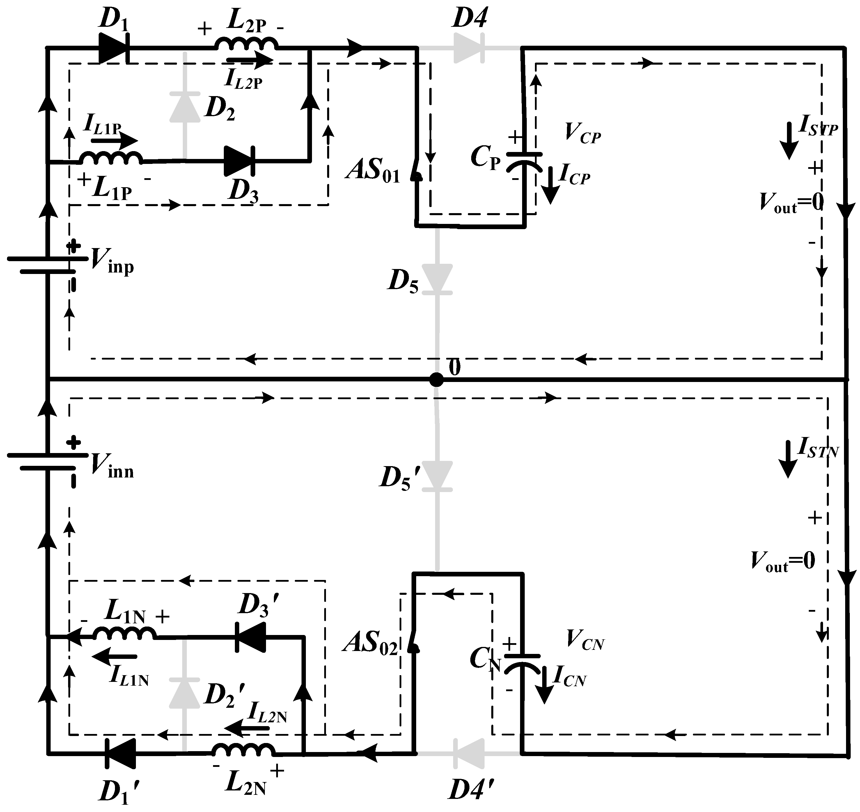
2.3. Shoot-Through (ST) State
3. Mathematical Analysis of the Proposed Inverter Topology
3.1. Non-ST-State
3.2. ST-State
3.3. Calculations of Current, Voltage, Boost Factor and Gain Factor
4. PWM and Boost Control Techniques
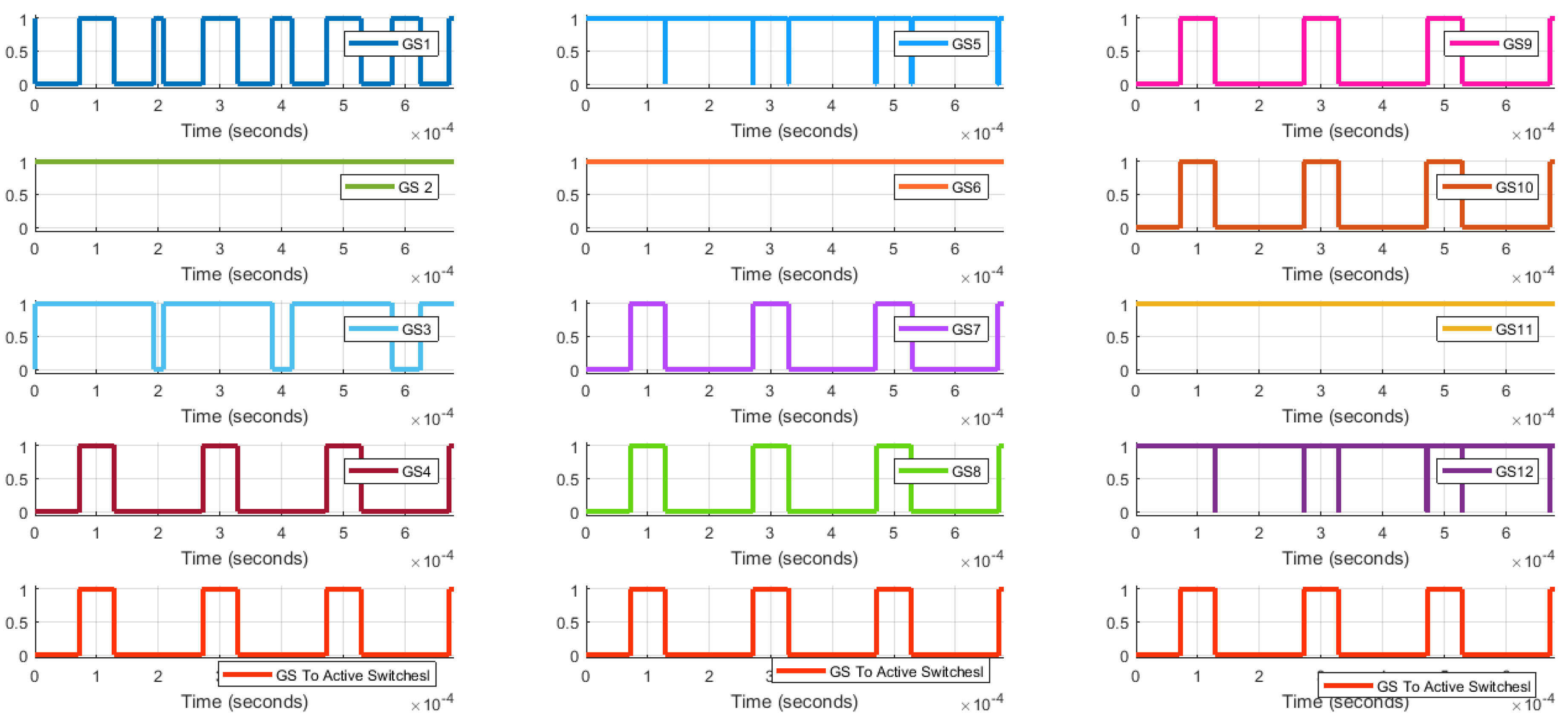
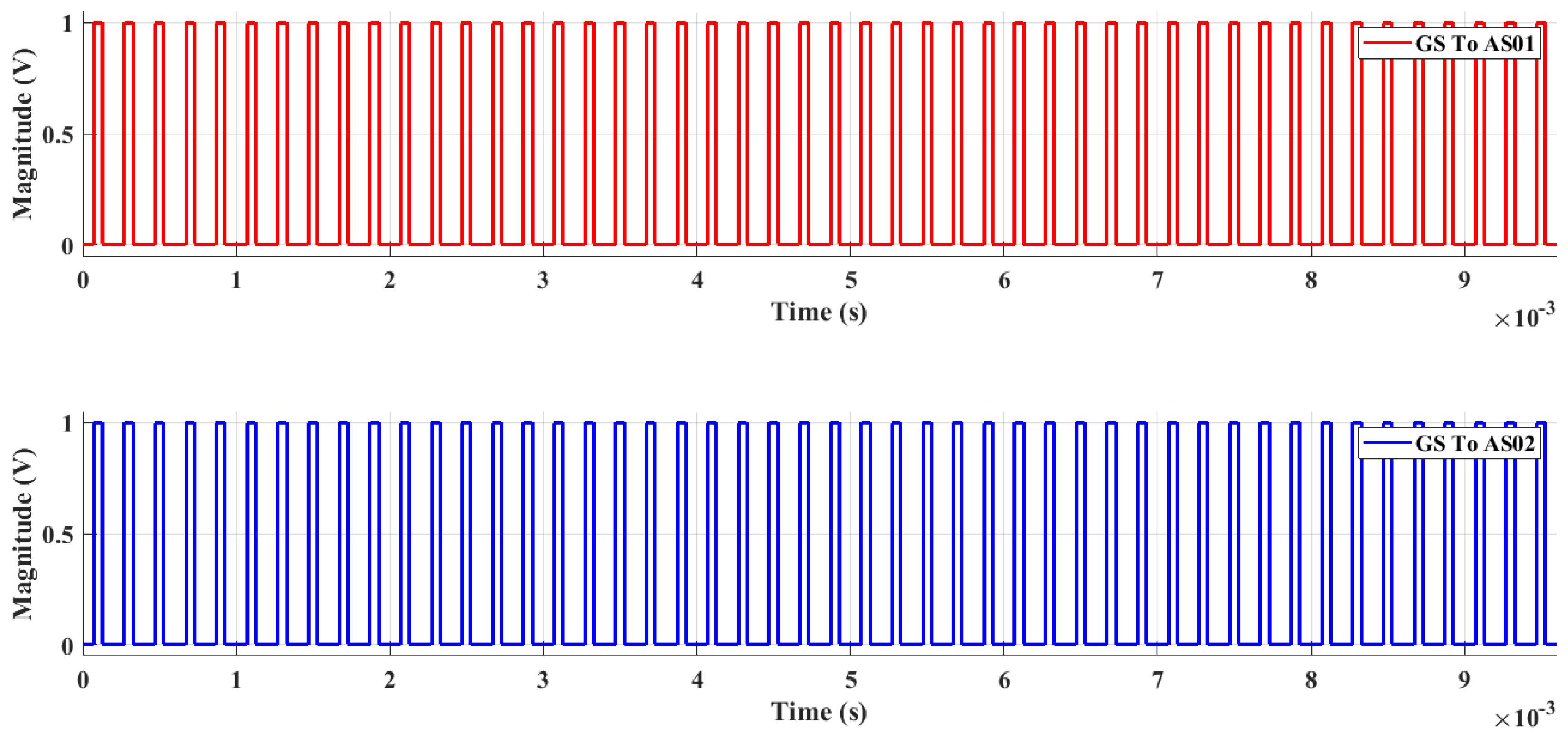
4.1. PWM Signals
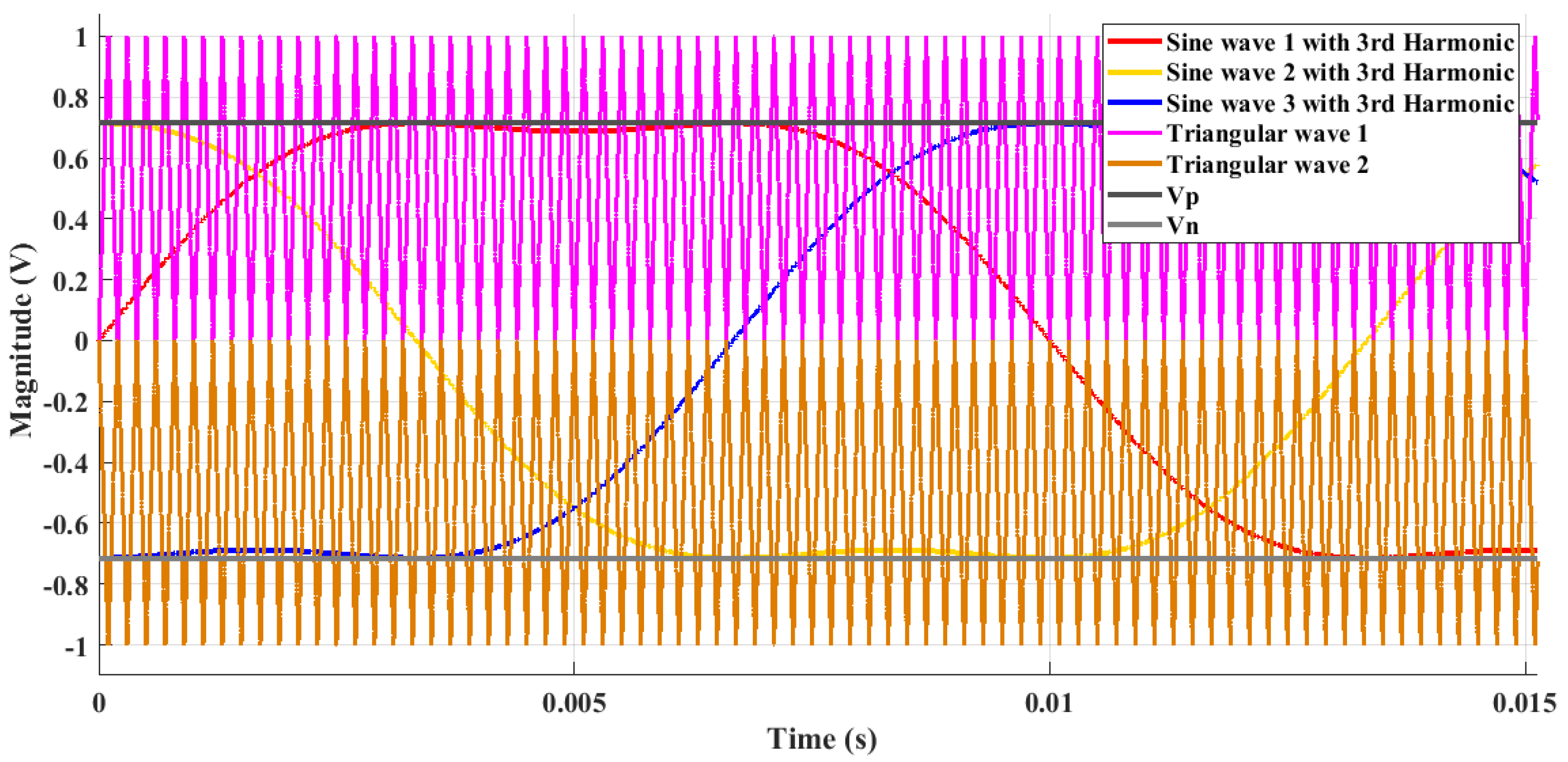
4.2. Maximum Constant Boost Control Method (MCBCM)
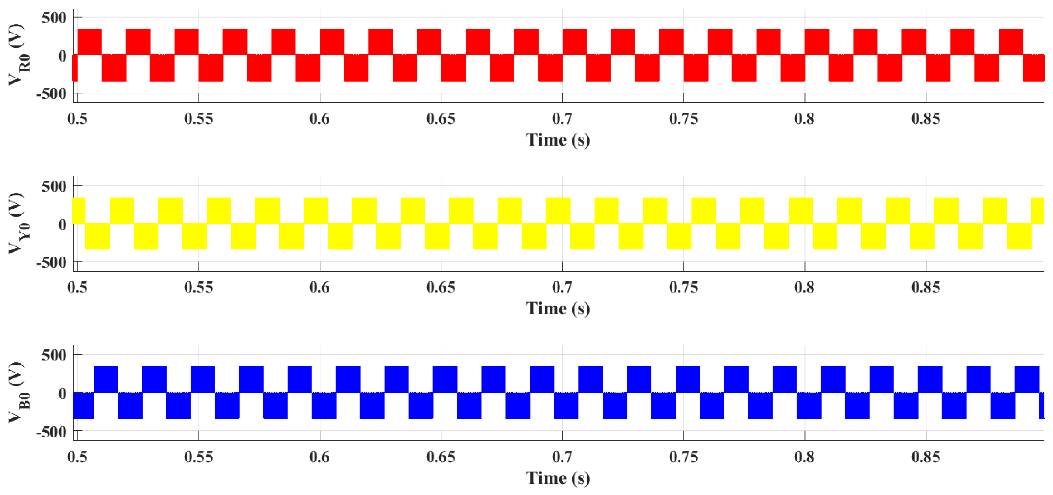
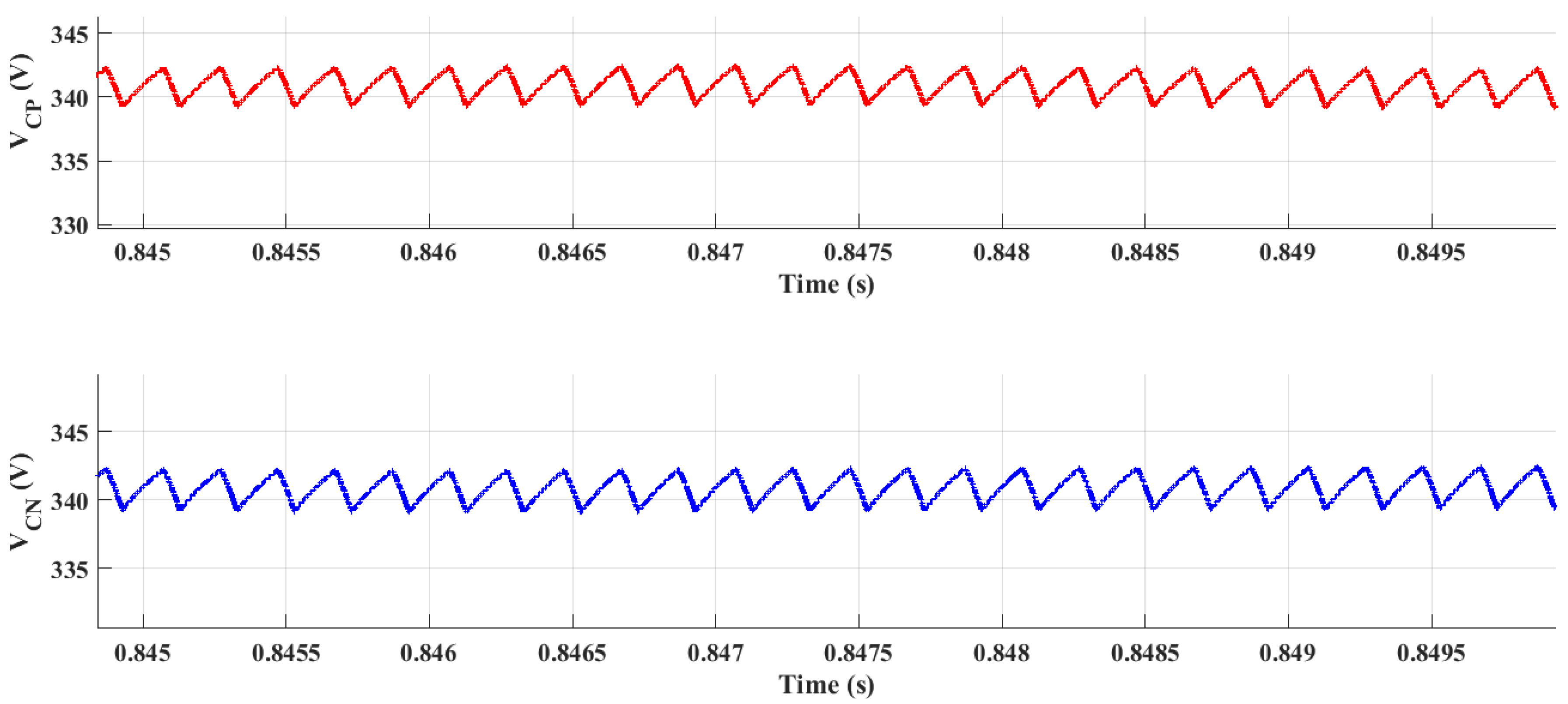
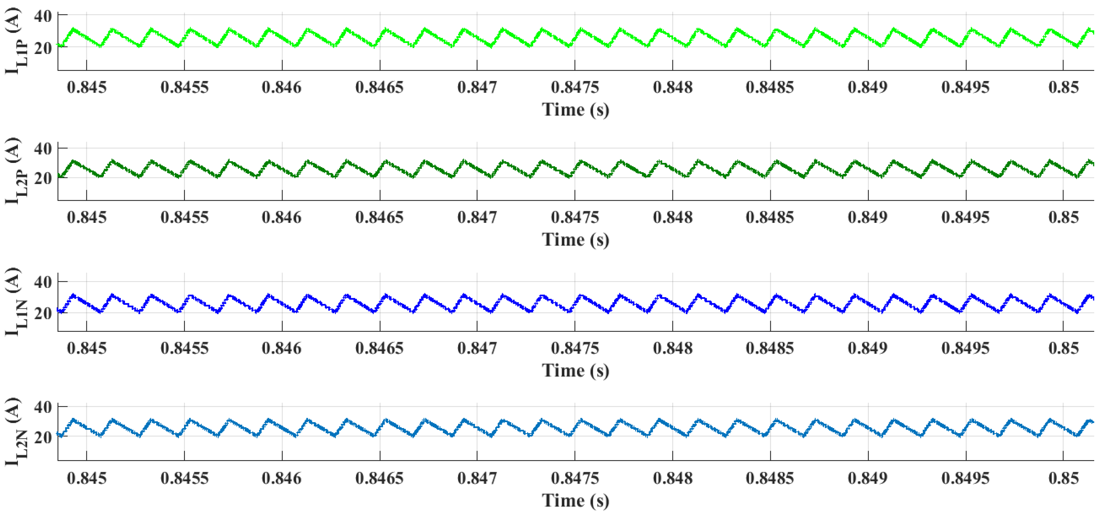
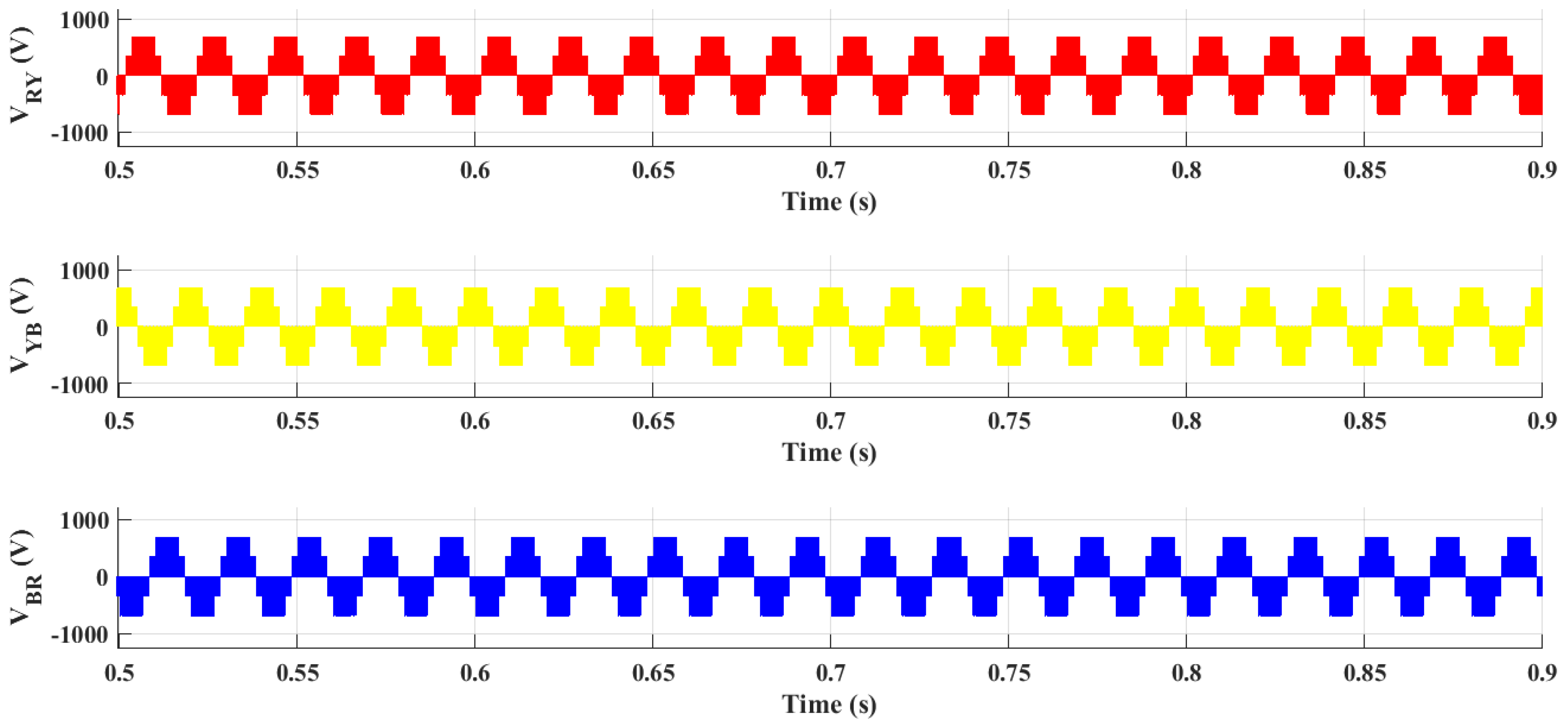
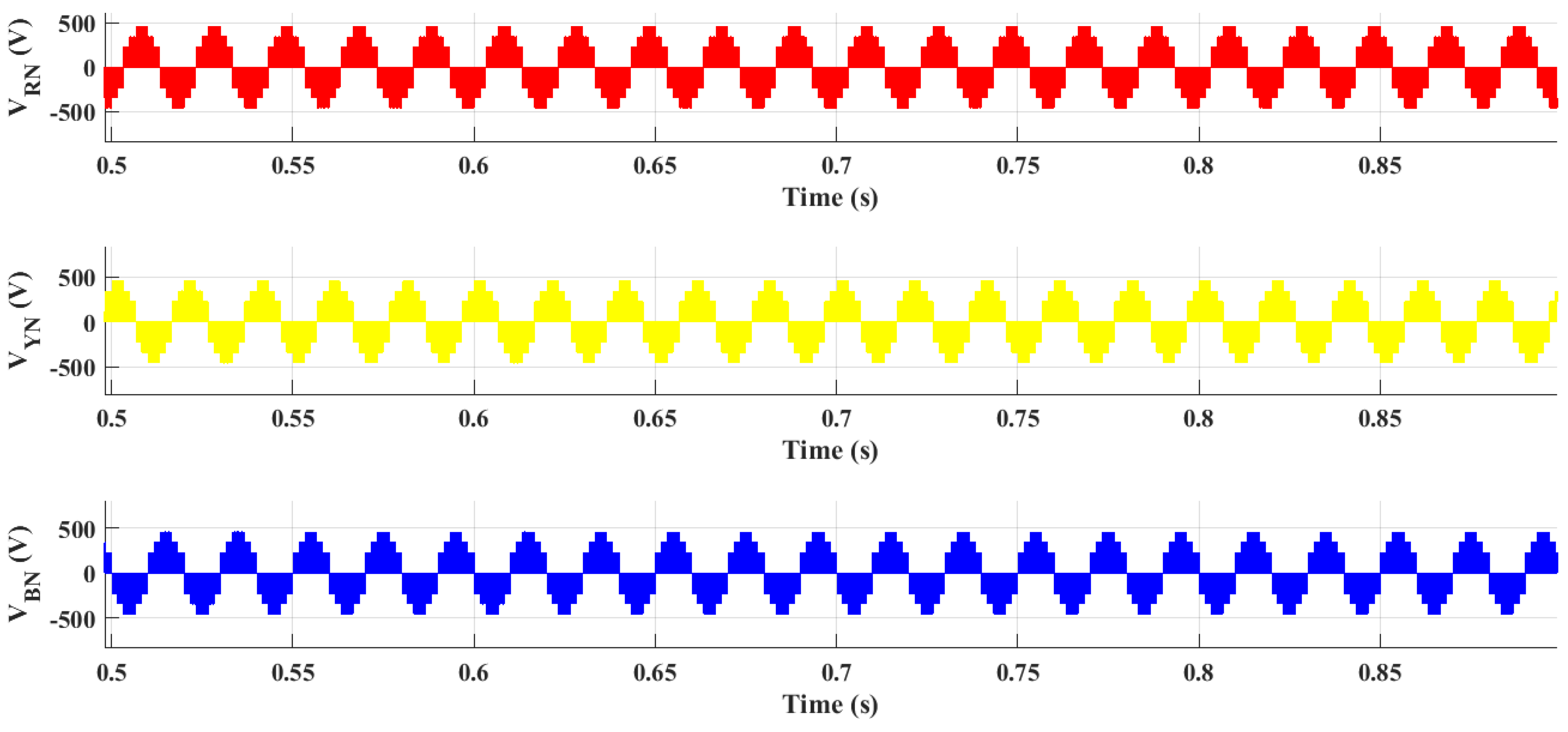
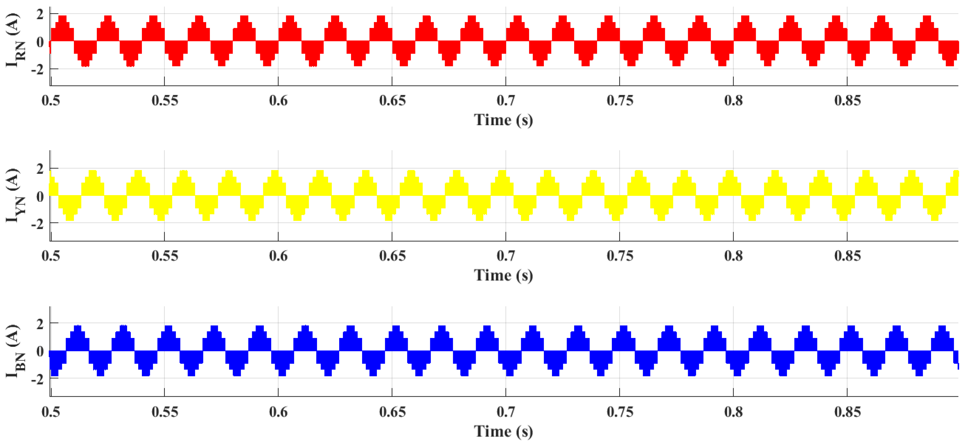
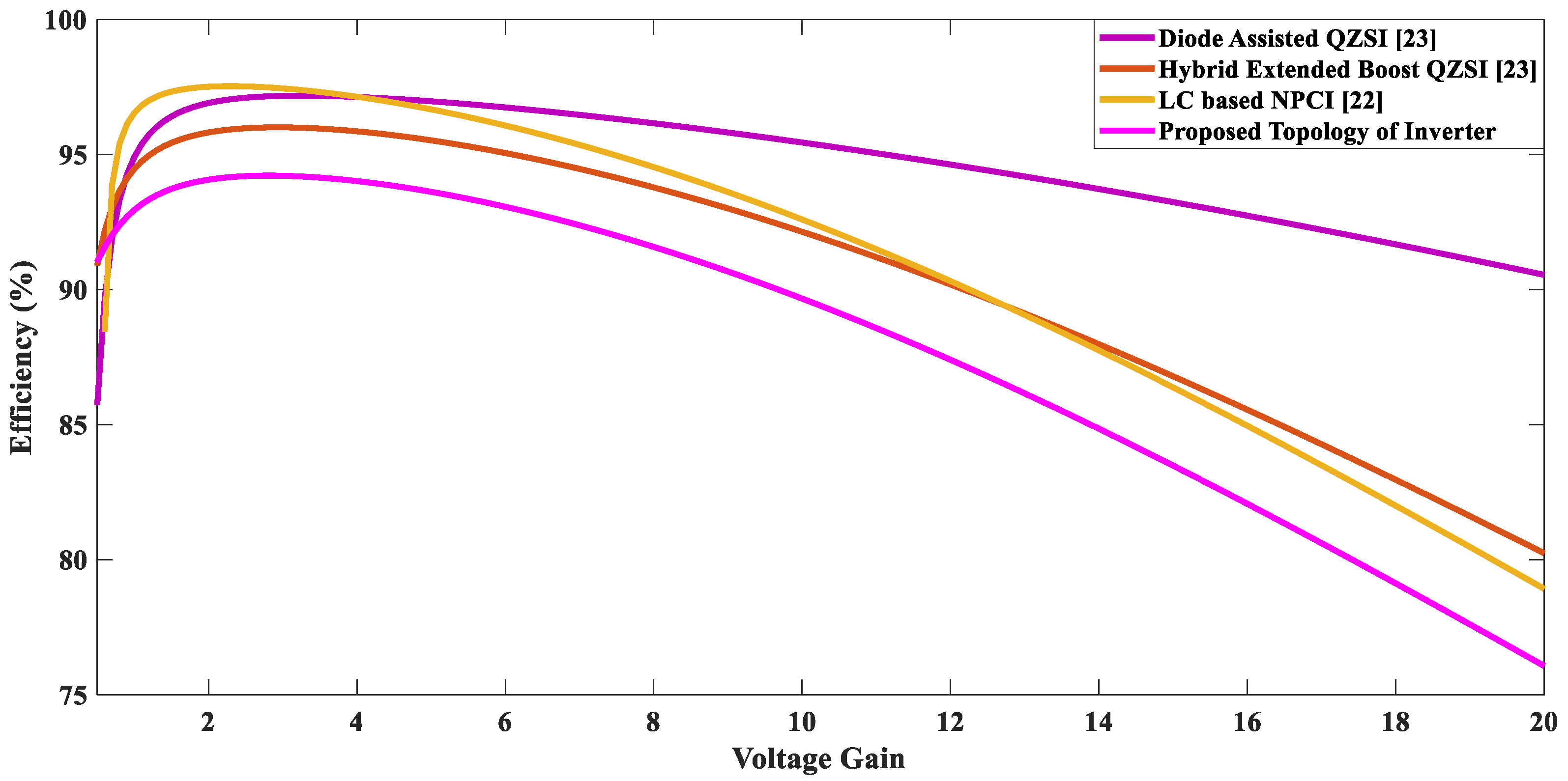
5. Simulations Results and Discussion
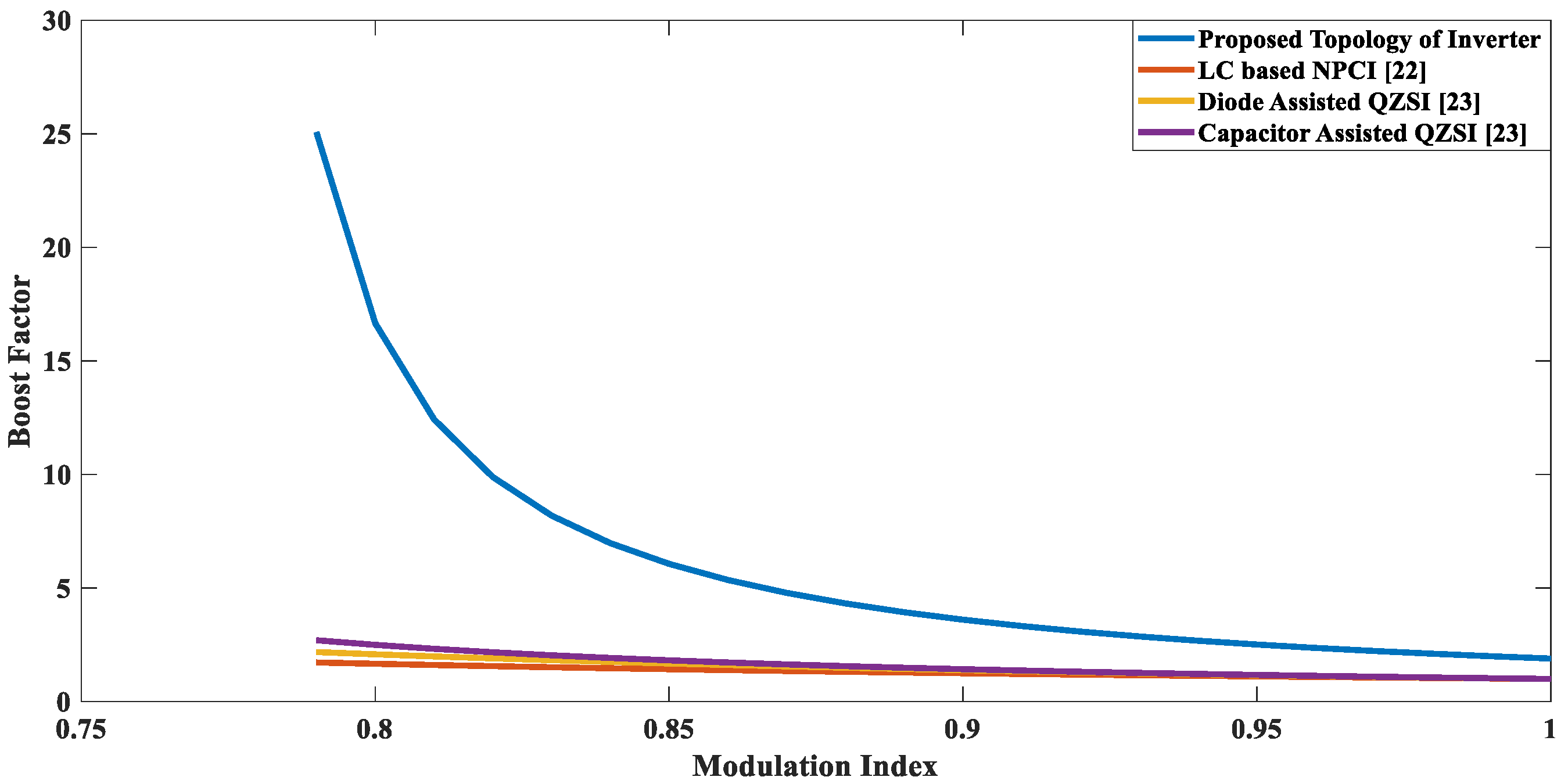
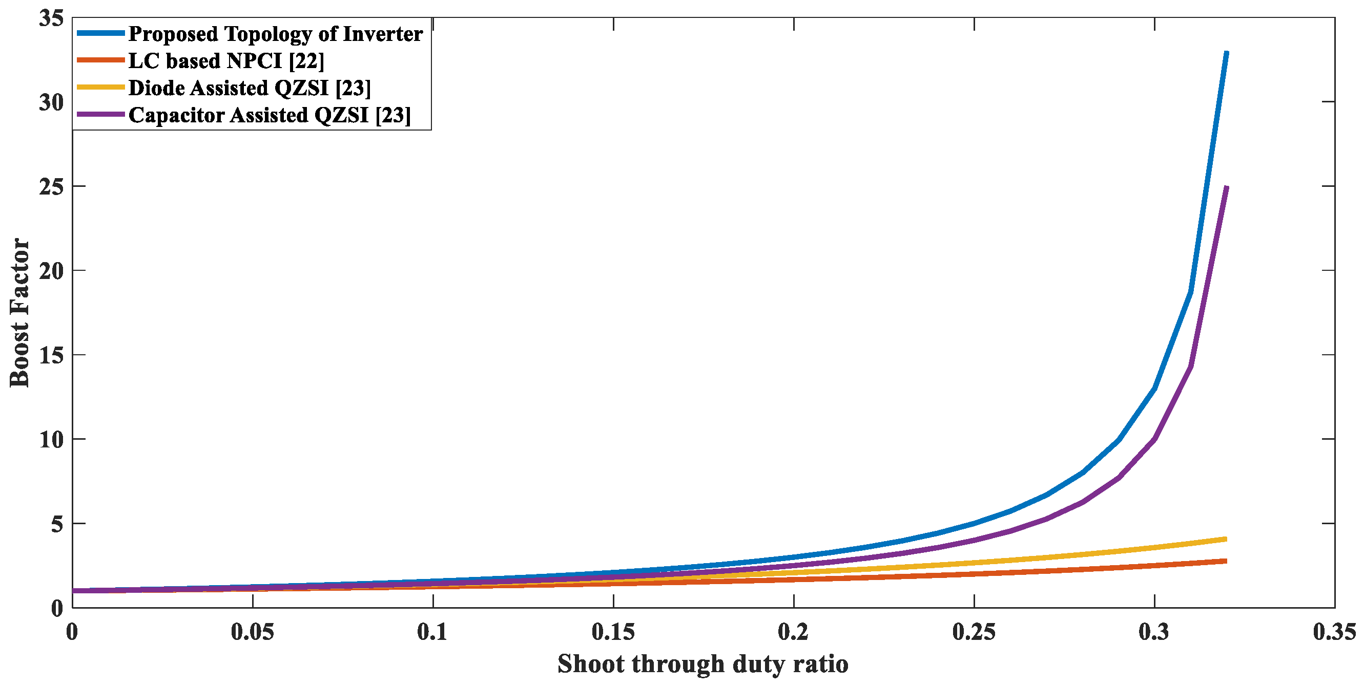
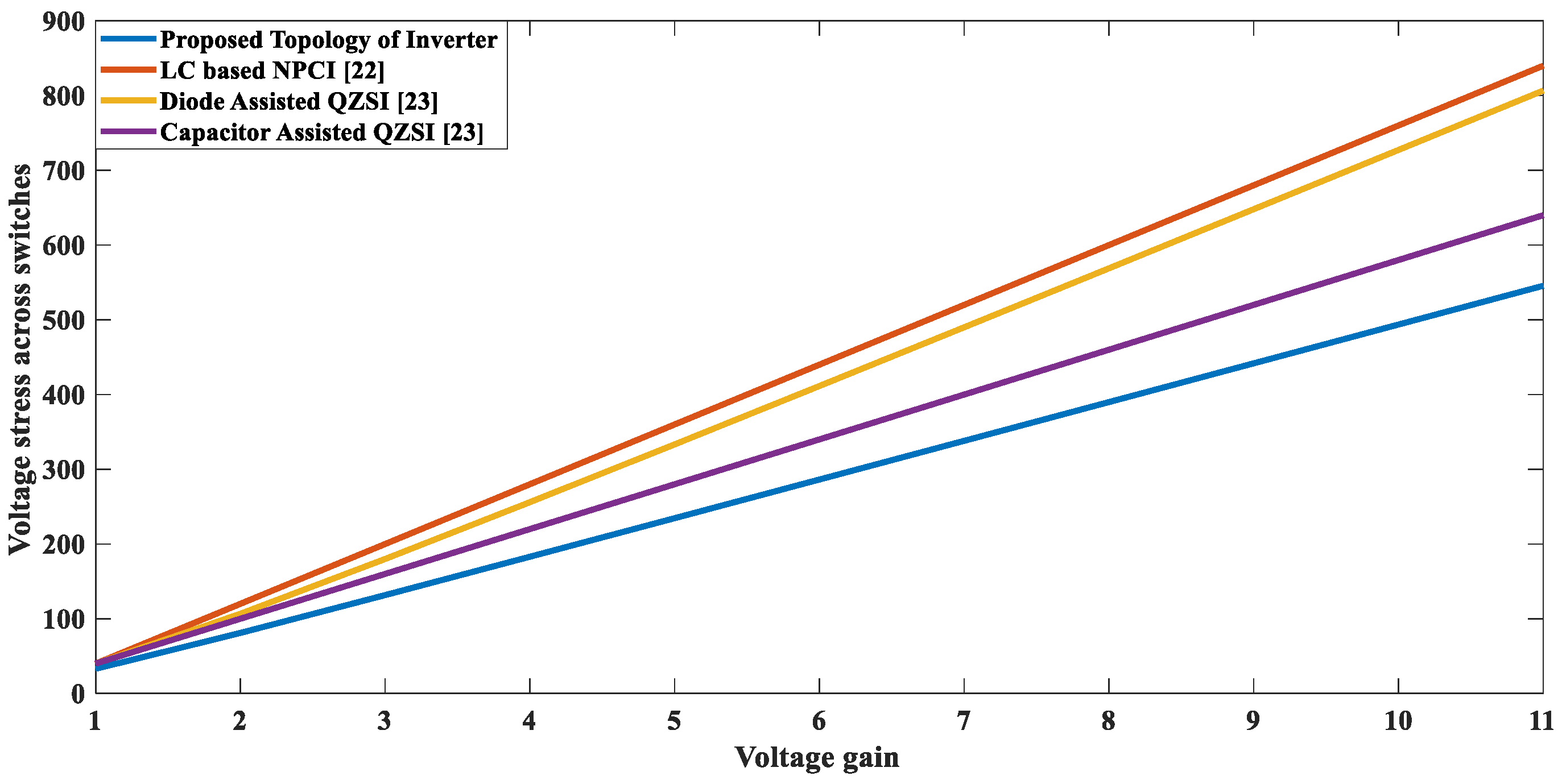
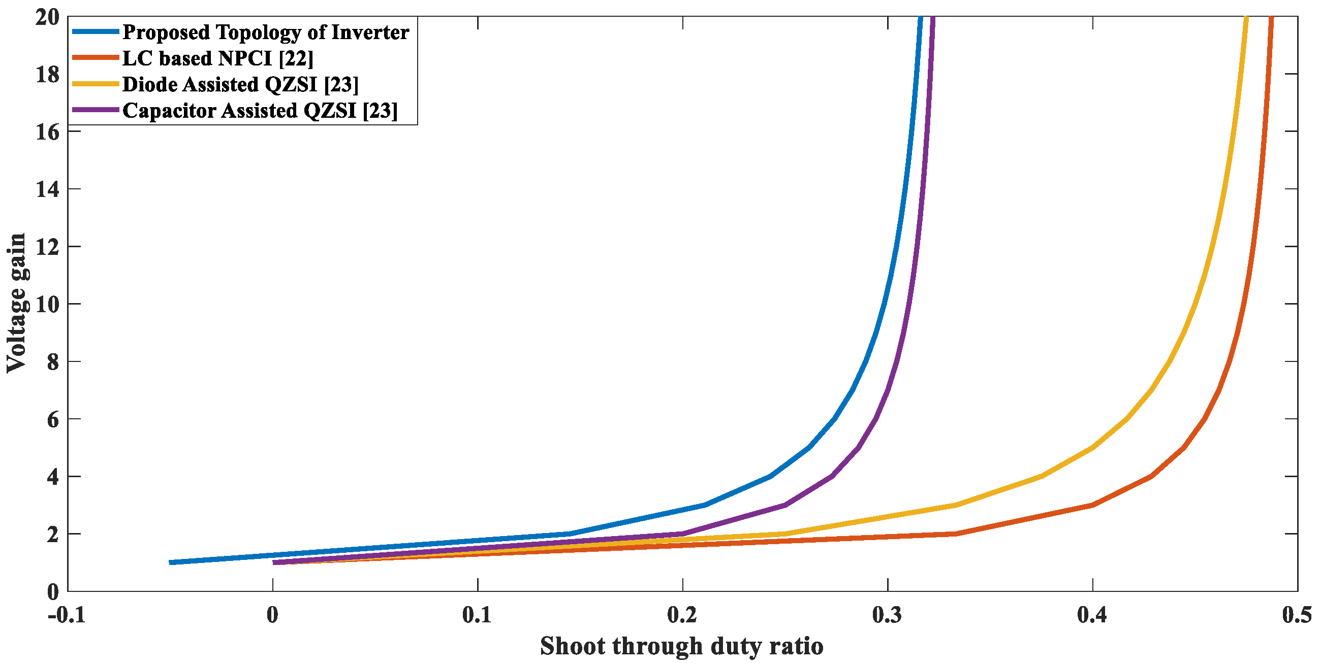
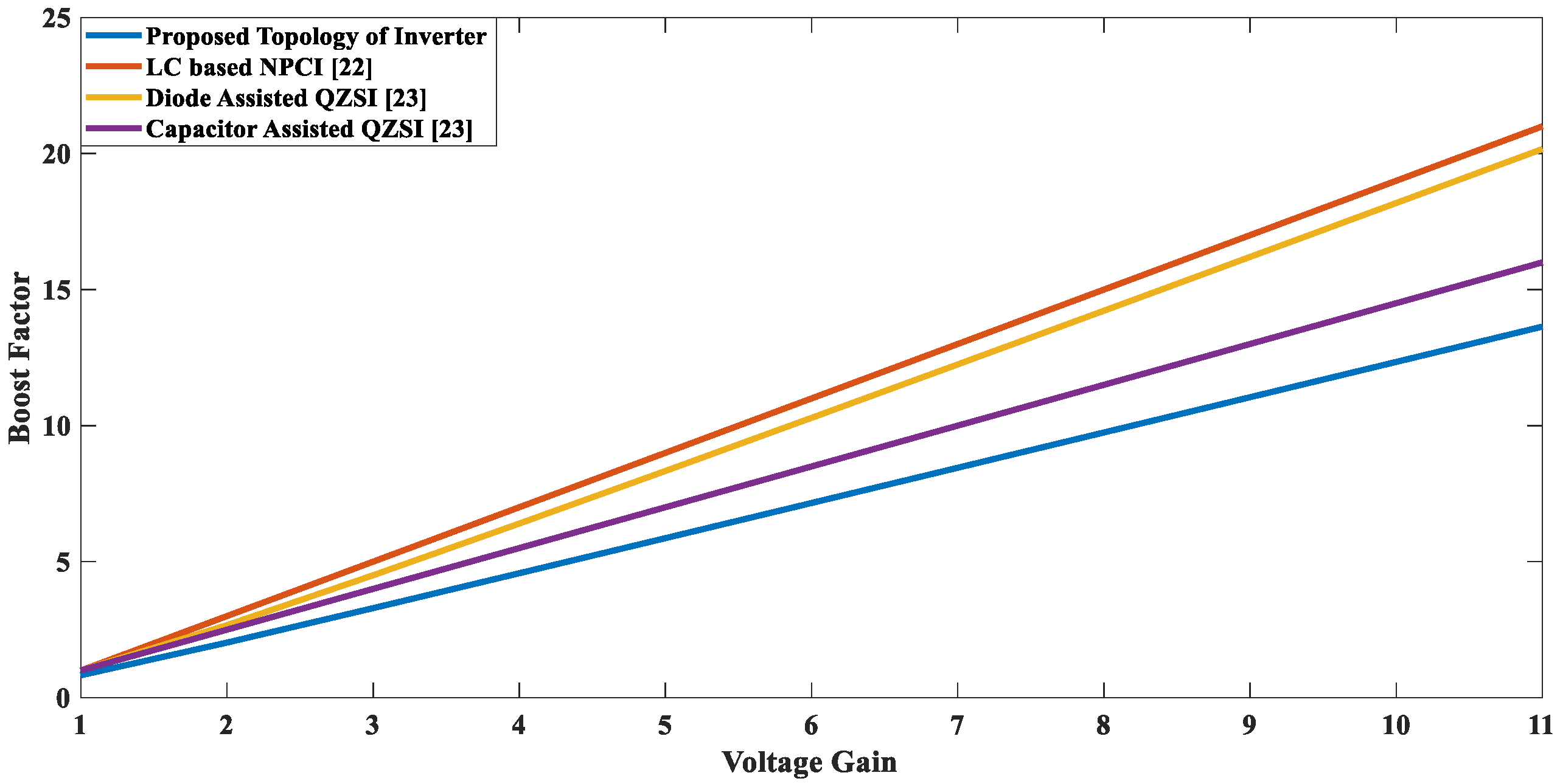
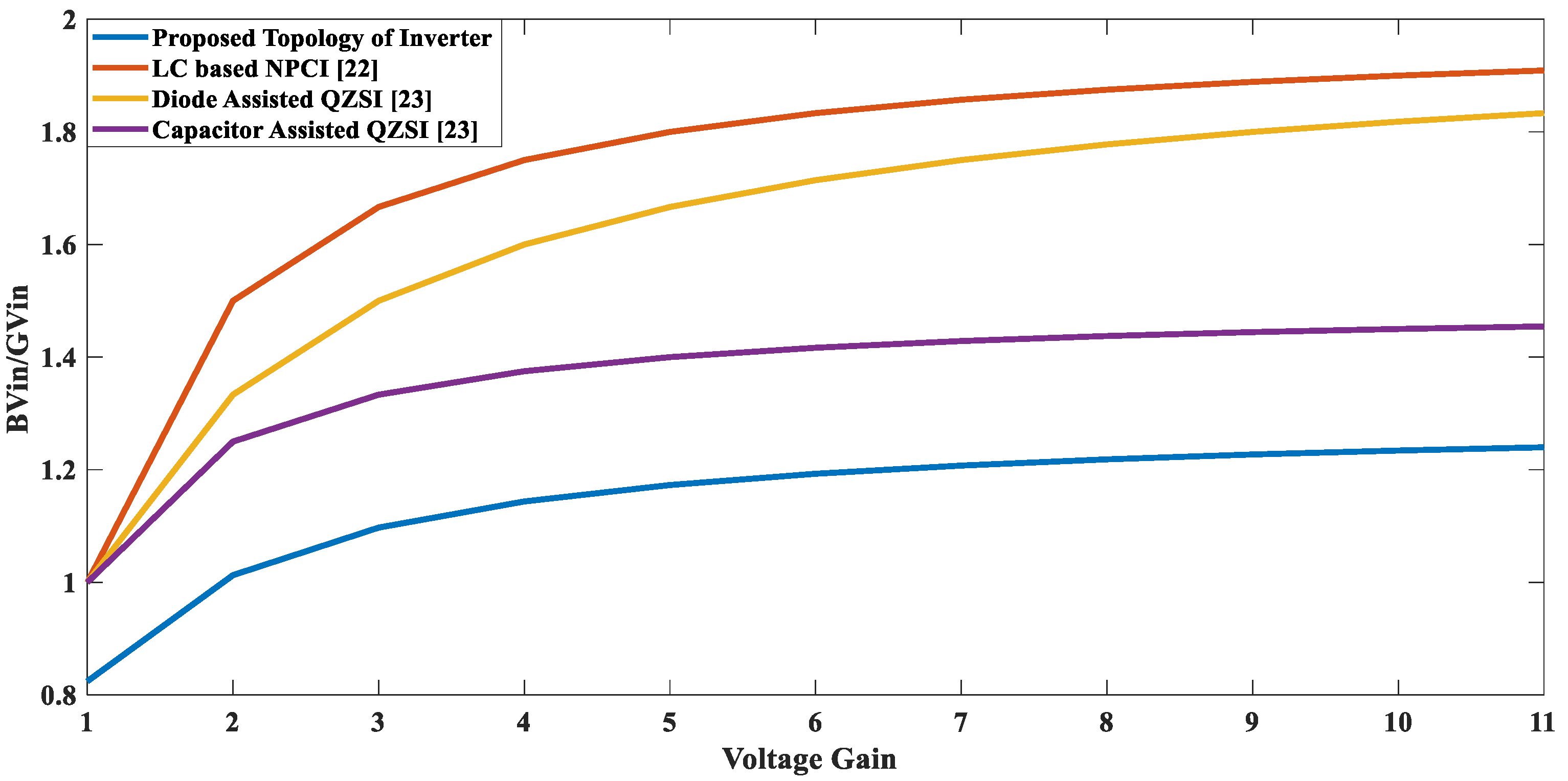
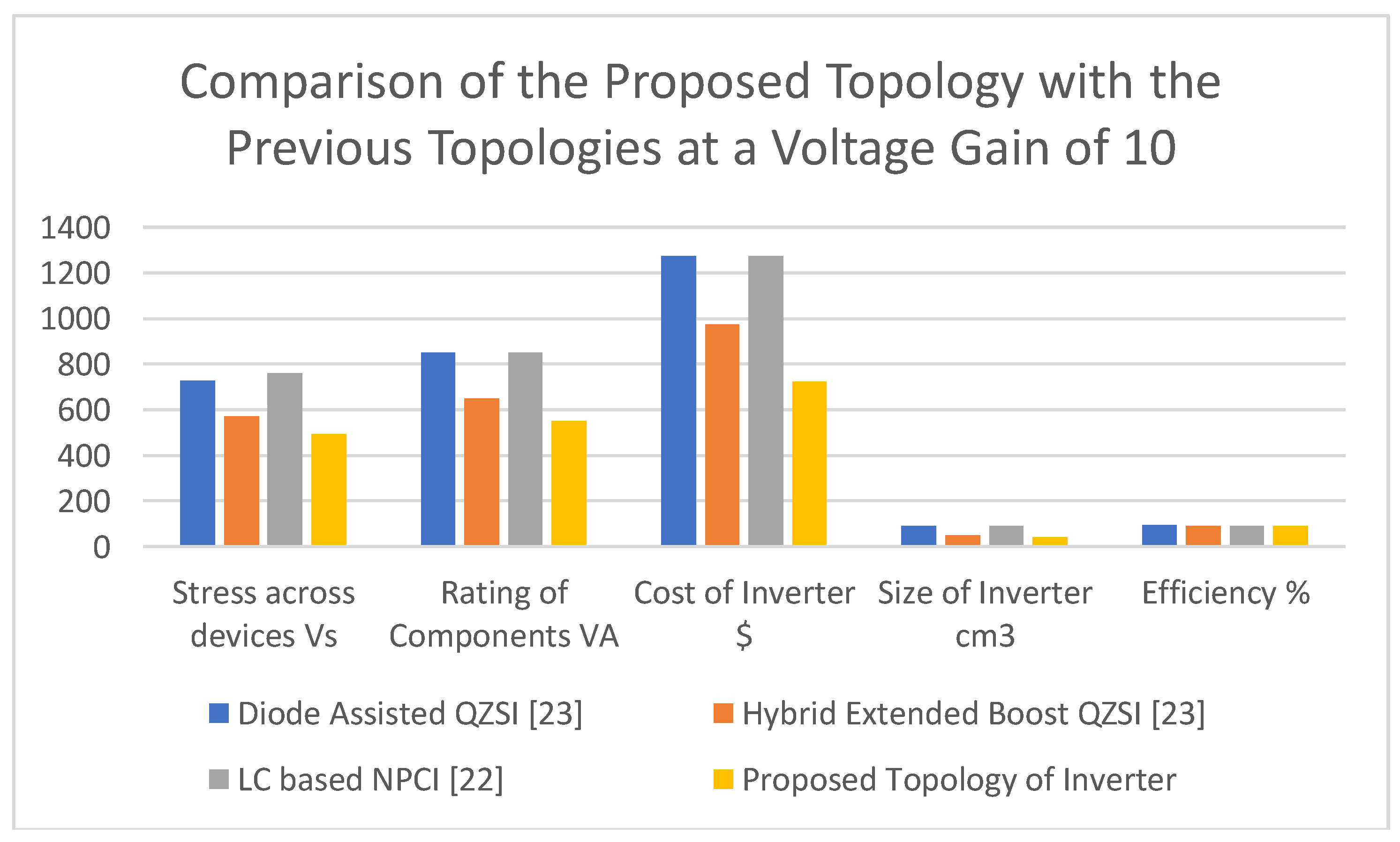
6. Comparison with Previous Topologies
7. Conclusions
Author Contributions
Funding
Conflicts of Interest
References
- Tang, Y.; Xie, S.; Zhang, C. An improved Z-source inverter. IEEE Trans. Power Electron. 2010, 26, 3865–3868. [Google Scholar] [CrossRef]
- Ding, X.; Qian, Z.; Yang, S.; Cui, B.; Peng, F. A high-performance Z-source inverter operating with small inductor at wide-range load. In Proceedings of the APEC 07-Twenty-Second Annual IEEE Applied Power Electronics Conference and Exposition, Anaheim, CA, USA, 25 Feburary–1 March 2007; pp. 615–620. [Google Scholar]
- Tang, Y.; Xie, S.; Zhang, C.; Xu, Z. Improved Z-source inverter with reduced Z-source capacitor voltage stress and soft-start capability. IEEE Trans. Power Electron. 2009, 24, 409–415. [Google Scholar] [CrossRef]
- Vinnikov, D.; Roasto, I.; Jalakas, T. An improved high-power DC/DC Converter for distributed power generation. In Proceedings of the 2009 10th International Conference on Electrical Power Quality and Utilisation, Lodz, Poland, 15–17 September 2009; pp. 1–6. [Google Scholar]
- Anderson, J.; Peng, F.Z. A class of quasi-Z-source inverters. In Proceedings of the 2008 IEEE Industry Applications Society Annual Meeting, Edmonton, AB, Canada, 5–9 October 2008; pp. 1–7. [Google Scholar]
- Anderson, J.; Peng, F.Z. Four quasi-Z-source inverters. In Proceedings of the 2008 IEEE Power Electronics Specialists Conference, Rhodes, Greece, 15–19 June 2008; pp. 2743–2749. [Google Scholar]
- Peng, F.Z.; Yuan, X.; Fang, X.; Qian, Z. Z-source inverter for adjustable speed drives. IEEE Power Electron. Lett. 2003, 1, 33–35. [Google Scholar] [CrossRef]
- Li, Y.; Anderson, J.; Peng, F.Z.; Liu, D. Quasi-Z-source inverter for photovoltaic power generation systems. In Proceedings of the 2009 Twenty-Fourth Annual IEEE Applied Power Electronics Conference and Exposition, Washington, DC, USA, 15–19 February 2009; pp. 918–924. [Google Scholar]
- Ismeil, M.A.; Kouzou, A.; Kennel, R.; Abu-Rub, H.; Orabi, M. A new switched-inductor quasi-Z-source inverter topology. In Proceedings of the 2012 15th International Power Electronics and Motion Control Conference (EPE/PEMC), Novi Sad, Serbia, 4–6 September 2012; pp. DS3d.2-1–DS3d.2-6. [Google Scholar]
- Mosa, M.; Abu-Rub, H.; Rodríguez, J. High performance predictive control applied to three phase grid connected Quasi-Z-Source Inverter. In Proceedings of the IECON 2013-39th Annual Conference of the IEEE Industrial Electronics Society, Vienna, Austria, 10–13 November 2013; pp. 5812–5817. [Google Scholar]
- Loh, P.C.; Gao, F.; Blaabjerg, F.; Goh, A.L. Buck-boost impedance networks. In Proceedings of the 2007 European Conference on Power Electronics and Applications, Aalborg, Denmark, 2–5 September 2007; pp. 1–10. [Google Scholar]
- Loh, P.C.; Gao, F.; Blaabjerg, F. Embedded EZ-source inverters. IEEE Trans. Ind. Appl. 2009, 46, 256–267. [Google Scholar]
- Loh, P.C.; Gao, F.; Blaabjerg, F.; Feng, S.Y.C.; Soon, K.N.J. Pulsewidth-Modulated $ Z $-Source Neutral-Point-Clamped Inverter. IEEE Trans. Ind. Appl. 2007, 43, 1295–1308. [Google Scholar] [CrossRef]
- Loh, P.C.; Blaabjerg, F.; Wong, C.P. Comparative evaluation of pulse-width modulation strategies for Z-source neutral-point-clamped inverter. In Proceedings of the 2006 37th IEEE Power Electronics Specialists Conference, Jeju, Korea, 18–22 June 2006; pp. 1–7. [Google Scholar]
- Loh, P.C.; Lim, S.W.; Gao, F.; Blaabjerg, F. Three-level Z-source inverters using a single LC impedance network. IEEE Trans. Power Electron. 2007, 22, 706–711. [Google Scholar] [CrossRef]
- Loh, P.C.; Gao, F.; Blaabjerg, F.; Lim, S.W. Operational analysis and modulation control of three-level Z-source inverters with enhanced output waveform quality. IEEE Trans. Power Electron. 2009, 24, 1767–1775. [Google Scholar] [CrossRef]
- Maheshwari, R.; Munk-Nielsen, S.; Busquets-Monge, S. Design of neutral-point voltage controller of a three-level NPC inverter with small DC-link capacitors. IEEE Trans. Ind. Electron. 2012, 60, 1861–1871. [Google Scholar] [CrossRef]
- Mo, W.; Loh, P.C.; Blaabjerg, F.; Wang, P. Trans-Z-source and Γ-Z-source neutral-point-clamped inverters. IET Power Electron. 2014, 8, 371–377. [Google Scholar] [CrossRef]
- Wang, X.; Liu, H.; Li, Y. A novel coupled inductor Z-source three-level inverter. IEICE Electron. Express 2017, 14. [Google Scholar] [CrossRef]
- Battiston, A.; Miliani, E.-H.; Pierfederici, S.; Meibody-Tabar, F. A novel quasi-Z-source inverter topology with special coupled inductors for input current ripples cancellation. IEEE Trans. Power Electron. 2015, 31, 2409–2416. [Google Scholar] [CrossRef] [Green Version]
- Yahya, A.; Waqar, T.; Husain, N.; Ali, S.M.U. Hybrid Multilevel Topology Based High Power Quality Inverter. In Proceedings of the APEC’98 Thirteenth Annual Applied Power Electronics Conference and Exposition, Anaheim, CA, USA, 15–19 February 1998. [Google Scholar]
- Sahoo, M.; Keerthipati, S. A three-level LC-switching-based voltage boost NPC inverter. IEEE Trans. Ind. Electron. 2016, 64, 2876–2883. [Google Scholar] [CrossRef]
- Gajanayake, C.J.; Luo, F.L.; Gooi, H.B.; So, P.L.; Siow, L.K. Extended-boost $ Z $-source inverters. IEEE Trans. Power Electron. 2010, 25, 2642–2652. [Google Scholar] [CrossRef]
- Peng, F.Z. Z-Source Inverter. IEEE Trans. Ind. Appl. 2003, 39. [Google Scholar] [CrossRef]
- Nabae, A.; Takahashi, I.; Akagi, H. A new neutral-point-clamped PWM inverter. IEEE Trans. Ind. Appl. 1981, 5, 518–523. [Google Scholar] [CrossRef]
- McGrath, B.P.; Holmes, D.G. Multicarrier PWM strategies for multilevel inverters. IEEE Trans. Ind. Electron. 2002, 49, 858–867. [Google Scholar] [CrossRef]
- Rathore, S.; Kirar, M.K.; Bhardwaj, S.K. Simulation of cascaded H-bridge multilevel inverter using PD, POD, APOD techniques. Electr. Comput. Eng. Int. J. ECIJ 2015, 4, 27–41. [Google Scholar] [CrossRef]
- Haskar Reddy, V.N.; Babu, C.S.; Suresh, K. Advanced Modulating Techniques for Diode Clamped Multilevel Inverter Fed Induction Motor. ARPN J. Eng. Appl. Sci. 2011, 6, 90–99. [Google Scholar]
- Colak, I.; Kabalci, E.; Bayindir, R. Review of multilevel voltage source inverter topologies and control schemes. Energy Convers. Manag. 2011, 52, 1114–1128. [Google Scholar] [CrossRef]
- McGrath, B.P.; Holmes, D.G. A comparison of multicarrier PWM strategies for cascaded and neutral point clamped multilevel inverters. In Proceedings of the 2000 IEEE 31st Annual Power Electronics Specialists Conference. Conference Proceedings (Cat. No. 00CH37018), Galway, Ireland, 23 June 2000; Volume 2, pp. 674–679. [Google Scholar]
- Peng, F.Z.; Shen, M.; Qian, Z. Maximum boost control of the Z-source inverter. IEEE Trans. Power Electron. 2005, 20, 833–838. [Google Scholar] [CrossRef]
- Shen, M.; Wang, J.; Joseph, A.; Peng, F.Z.; Tolbert, L.M.; Adams, D.J. Constant boost control of the Z-source inverter to minimize current ripple and voltage stress. IEEE Trans. Ind. Appl. 2006, 42, 770–778. [Google Scholar] [CrossRef]
- Pan, L. LZ-source inverter. IEEE Trans. Power Electron. 2014, 29, 6534–6543. [Google Scholar] [CrossRef]
- Zhu, X.; Zhang, B.; Qiu, D. Enhanced boost quasi-Z-source inverters with active switched-inductor boost network. IET Power Electron. 2018, 11, 1774–1787. [Google Scholar] [CrossRef]
- Rodriguez, J.; Lai, J.-S.; Peng, F.Z. Multilevel inverters: A survey of topologies, controls, and applications. IEEE Trans. Ind. Electron. 2002, 49, 724–738. [Google Scholar] [CrossRef] [Green Version]
- Peng, F.Z.; Joseph, A.; Wang, J.; Shen, M.; Chen, L.; Pan, Z.; Ortiz-Rivera, E.; Huang, Y. Z-source inverter for motor drives. IEEE Trans. Power Electron. 2005, 20, 857–863. [Google Scholar] [CrossRef]
- Khlebnikov, A.S.; Kharitonov, S.A. Application of the Z-source converter for aircraft power generation systems. In Proceedings of the 2008 9th International Workshop and Tutorials on Electron Devices and Materials, Novosibirsk, Russia, 1–5 July 2008; pp. 211–215. [Google Scholar]


| Sr. No. | ON Switches | OFF Switches |
|---|---|---|
| 1 | , , , , , | , , , , , , , |
| 2 | , , , , , | , , , , , , , |
| 3 | , , , , , | , , , , , , , |
| 4 | , , , , , , , , , | , , , |
| 5 | , , , , , , , , , | , , , |
| 6 | , , , , , , , , , | , , , |
| 7 | , , , , , , , , , , , , , | Nil |
| Parameters/Component | Value |
|---|---|
| Applied DC Voltage | 40 V |
| Capacitor | 1000 µF |
| Inductor | 2 mH |
| Load | 250 Ω |
| Frequency of Reference Signal(s) | 50 Hz |
| Frequency of Carrier Signal(s) | 5000 Hz |
| Modulation Index, M | 0.825 |
| Shoot Through Duty Ratio, D | 0.2855291 |
| Boost Factor | 8.96 |
| Overall Voltage Gain, G | 7.392 |
| Device | Parameter | Value |
|---|---|---|
| Diode | Internal Resistance | 0.001 Ω |
| Forward Voltage Drop | 0.7 V | |
| Snubber Resistance | 500 Ω | |
| Snubber Capacitance | inf | |
| Active Switch | Internal Resistance | 0.001 Ω |
| Snubber Resistance | 1 × 10⁵ Ω | |
| Snubber Capacitance | inf | |
| IGBT | Internal Resistance | 0.01 Ω |
| Snubber Resistance | 1 × 10⁵ Ω | |
| Snubber Capacitance | 1000 F |
| ST Duty Ratio (D) | Modulation Index (M) | Boost Factor (B) |
|---|---|---|
| 0.11 | 1.0277 | 1.6567 |
| 0.13 | 1.0046 | 1.8525 |
| 0.15 | 0.9815 | 2.0909 |
| 0.17 | 0.9584 | 2.3878 |
| 0.19 | 0.9353 | 2.7674 |
| 0.21 | 0.9122 | 3.2703 |
| 0.23 | 0.8891 | 3.9677 |
| 0.25 | 0.866 | 5.0 |
| 0.27 | 0.8429 | 6.6842 |
| 0.2855 | 0.825 | 8.96 |
| 0.29 | 0.8198 | 9.9231 |
| 0.31 | 0.7967 | 18.7143 |
| 0.32 | 0.7852 | 33 |
| 0.33 | 0.7736 | 133 |
| Parameter | Proposed Inverter Topology | LC-based NPCI [22] | Diode Assisted [23] QZSI | Capacitor Assisted QZSI [23] |
|---|---|---|---|---|
| Boost Factor | ||||
| Voltage Gain | ||||
| Modulation Index | ||||
| Shoot- Through Duty Ratio | ||||
| Stress Across Switches |
| Component/Parameter | Symbol | Value |
|---|---|---|
| ESR of Capacitor | RC | 0.08 Ω |
| DCR of Inductor | RL | 0.07 Ω |
| On-Resistance of Active Switch | RS | 0.001 Ω |
| Load Resistance | Rl | 250 Ω |
| Applied DC Voltage | Vin | 40 V |
| Voltage Drop Across Diode | VF | 0.7 V |


© 2020 by the authors. Licensee MDPI, Basel, Switzerland. This article is an open access article distributed under the terms and conditions of the Creative Commons Attribution (CC BY) license (http://creativecommons.org/licenses/by/4.0/).
Share and Cite
Aqeel Anwar, M.; Abbas, G.; Khan, I.; Awan, A.B.; Farooq, U.; Saleem Khan, S. An Impedance Network-Based Three Level Quasi Neutral Point Clamped Inverter with High Voltage Gain. Energies 2020, 13, 1261. https://doi.org/10.3390/en13051261
Aqeel Anwar M, Abbas G, Khan I, Awan AB, Farooq U, Saleem Khan S. An Impedance Network-Based Three Level Quasi Neutral Point Clamped Inverter with High Voltage Gain. Energies. 2020; 13(5):1261. https://doi.org/10.3390/en13051261
Chicago/Turabian StyleAqeel Anwar, Muhammad, Ghulam Abbas, Irfan Khan, Ahmed Bilal Awan, Umar Farooq, and Saad Saleem Khan. 2020. "An Impedance Network-Based Three Level Quasi Neutral Point Clamped Inverter with High Voltage Gain" Energies 13, no. 5: 1261. https://doi.org/10.3390/en13051261
APA StyleAqeel Anwar, M., Abbas, G., Khan, I., Awan, A. B., Farooq, U., & Saleem Khan, S. (2020). An Impedance Network-Based Three Level Quasi Neutral Point Clamped Inverter with High Voltage Gain. Energies, 13(5), 1261. https://doi.org/10.3390/en13051261