1. Introduction
The voltage synchronous phase is one of the key signals of converter control systems in distributed power generation systems. It is of paramount importance to detect the voltage phase quickly and accurately for high-performance system control strategies [
1,
2]. In recent years, increasing numbers of power electronic devices have been put into operation for electricity transformation in the power system. However, the collected power voltage signal often contains high-frequency random noise, which greatly interferes with the accurate detection of the voltage phase and becomes an unfavorable factor for achieving the high-performance control of grid-connected inverters [
3,
4,
5]. Thus, phase detection schemes should have excellent noise immunity to suppress the interference.
In practical terms, phase detection schemes can be divided into open-loop phase detection (OPD) and closed-loop phase detection (CPD). The open-loop phase detection scheme eliminates the PI adjustment process, which can realize the rapid detection of the voltage phase. It is always applied to conditions such as a relatively ideal grid environment, and the requirement of phase accuracy is not very high [
6,
7,
8]. A zero-crossing phase detection scheme is suggested in [
8], which is the most commonly used OPD scheme at present. Its basic principle is to take the zero-crossing point as the reference point, and then the grid voltage phase can be calculated at each moment. However, high-frequency noise will affect the accurate detection of the zero-crossing point and result in phase detection errors. An OPD scheme based on the dq frame is given in [
9], which focuses on the phase detection of single-phase voltage. In [
9], a voltage signal is substituted into the rotational dq frame and converted into the voltage DC component. Then, the single-phase voltage can be quickly determined by a simple calculation. However, it is observed that noise will cause a DC component error after abc/dq transformation, which will thus result in a phase error. Moreover, at least two-phase orthogonal signals are required to complete the coordinate transformation. Delaying the sampling period to construct an orthogonal signal will result in high-frequency noise amplification, which thus further causes phase steady-state error [
4]. In [
10], the authors focus on the rapid phase detection of unbalanced grid voltage, which significantly improves the phase detection speed under complex conditions. However, while extracting the voltage-positive sequence components, random noise may still be amplified during the construction of the orthogonal voltage signal by delaying the sampling period or the first-order differentiating method [
11].
An OPD based on the dq frame scheme has advantages in terms of obtaining the real-time voltage phase and dealing with frequency step changes or phase jumps, and it can realize the fast detection of voltage phases and ensure the superiority of a grid-tied converter control system under adverse grid conditions. However, high-frequency noise is a factor which cannot be ignored and will cause fluctuation changes in the voltage current magnitude and thus result in phase detection errors. A low-pass filter (LPF) is introduced as an effective solution to attenuate high-frequency random noise [
9,
10,
11,
12]. Reducing the filter bandwidth can effectively suppress noise; however, it will limit the dynamic performance of the control system at the same time, which leads to a longer system dynamic response time.
Noise immunity is a key part in the higher phase accuracy of an open-loop phase detection scheme based on a dq frame. Therefore, it is very important not only to study the influencing factors of noise immunity in detail but also to effectively suppress high-frequency noise to reduce phase error and simultaneously ensure the rapidity of phase detection methods.
The paper is organized as follows.
Section 2 presents the basic principle of the dq frame-based OPD scheme suggested in [
9,
10].
Section 3 establishes a detailed phase error analysis model to evaluate the noise immunity of OPD. The improved OPD algorithm achieved by fine-tuning the rotation angle of the dq frame is presented in
Section 4. MATLAB/RT-LAB simulation studies for the enhanced algorithm are presented in
Section 5. Conclusions are given in
Section 6.
2. Basic Principles of OPD
First, three-phase balanced voltages can be described by
where
Um,
ω and
θ represent the voltage magnitude, the gird frequency and initial phase, respectively.
Using Clarke’s and Park’s transformation, the voltages
U = [
Ua Ub Uc]
T in Equation (1) are transformed as
Ud and
Uq as follows:
The DC components of the three-phase voltages can thus be expressed as
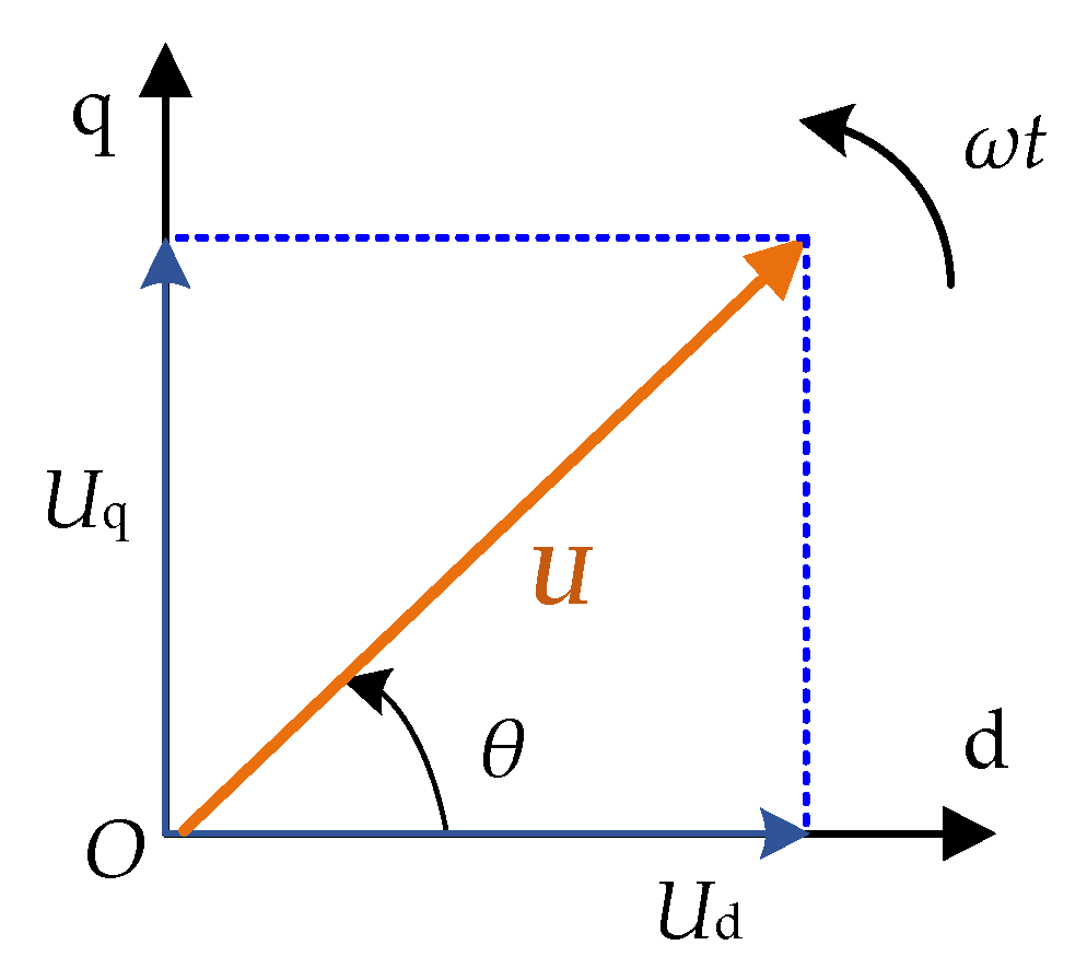
From
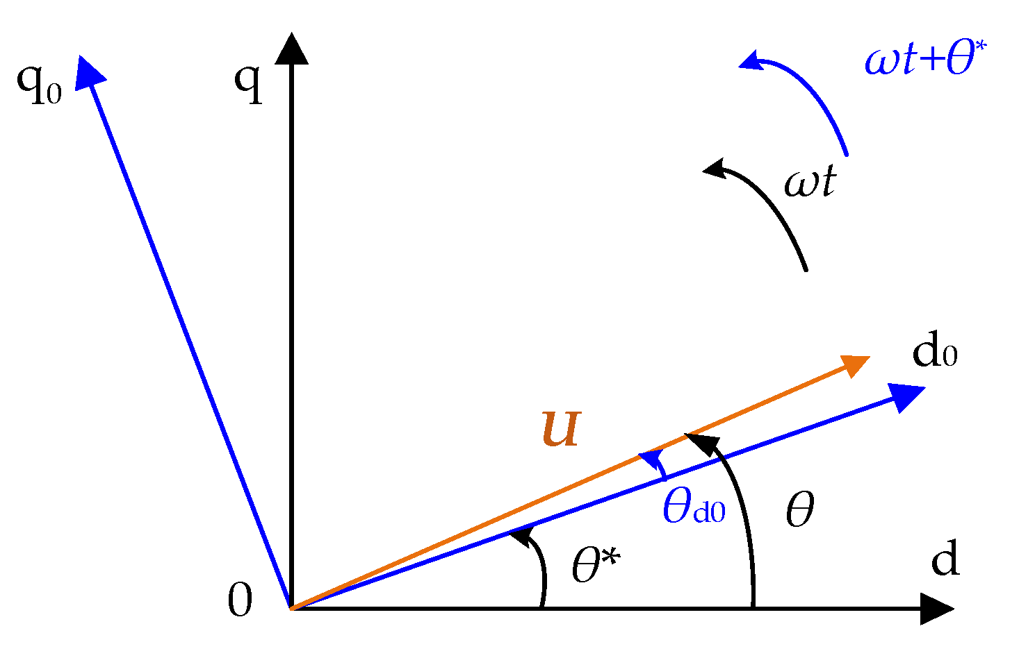
Figure 1, it can be seen that the initial phase
θ of the three-phase gird voltages is the angle between
U and the d axis.
The voltage initial phase
θ can thus be captured by
We define the initial phase angle as agreeing with [0, 2π); however, the phase computed by Equation (4) belongs to (–π/2, π/2). To convert the initial angles to the set interval, this paper employs a compensation phase
θex, which is defined by
In summary, the current position of the three-phase voltages can thus be computed as
Similarly, the magnitude of grid voltages also can be computed as
For the ideal grid voltage conditions without high-frequency random noise interference, substitute Equation (1) into Equations (2), (5) and (7); the instantaneous magnitude and synchronous phase can be captured immediately and accurately, respectively.
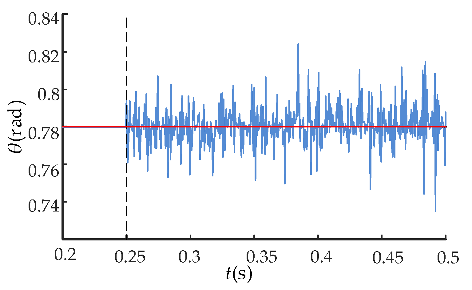
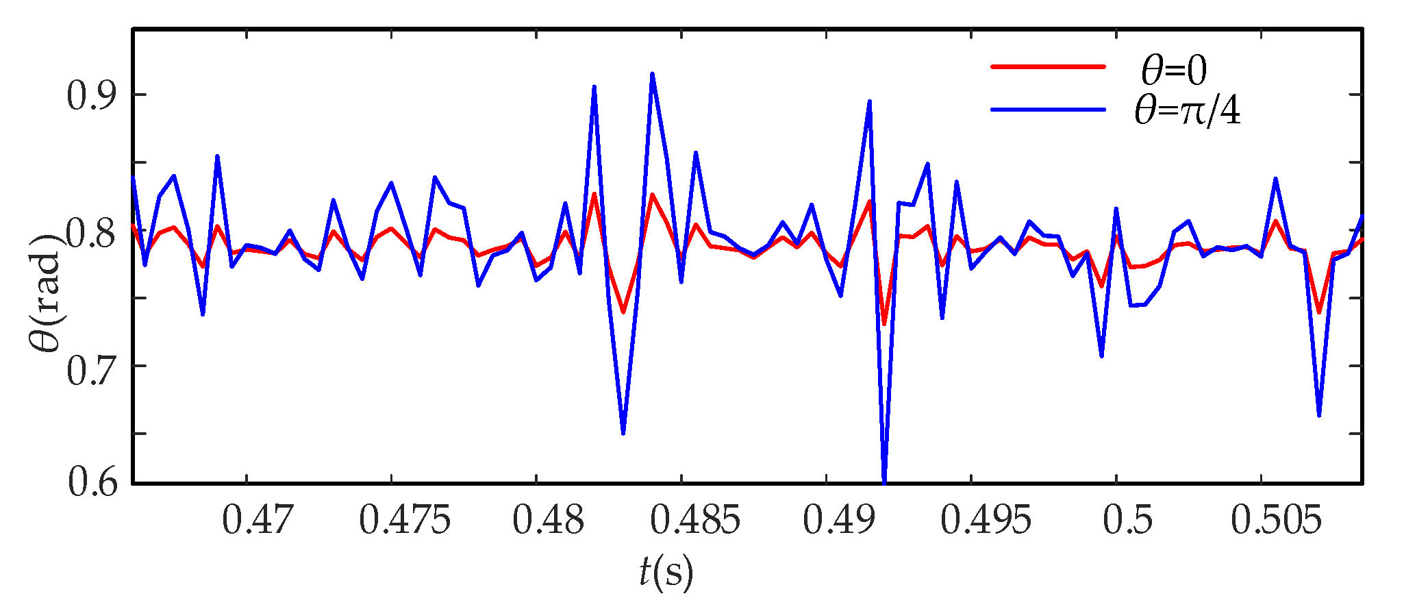
However, when noise interference occurs, the computed magnitude of the grid voltages undoubtedly contains random fluctuations. As shown in
Figure 2, the actual detection phase computed by Equation (4) thus offsets the actual value, which results in an obvious phase error.
In brief, the OPD based on the dq frame exhibits the advantages of rapidity and simplicity, which can detect voltage synchronous phase faster than traditional CPDs and thus ensure the high-performance operation of grid-connected inverters. It is worth noticing that the important premise of improving phase measurement accuracy is to ensure the rapidity of the OPD scheme under noise conditions. Based on this premise, it is necessary to evaluate the noise immunity and thus propose an enhanced scheme to ensure that the phase error is acceptable.
3. Noise Immunity Analysis Model of OPD
The gird voltages are regarded as the combination of the three-phase balanced grid voltages and the high-frequency noise DC components. Thus, the three-phase voltage signal with high-frequency noise could be described as
The physical quantities with superscript ∼ in this paper indicate the existence of random noise.
Considering the existence of high-frequency random noise, Equation (4) can be rewritten as
In Equation (9),
xq and
xd denote noise values in the dq frame, respectively.
θ* is the actual detection phase. Assume
xq ≤
N,
xd ≤
N, where
N is the possible maximum noise value; to analyze the noise immunity systematically in this paper, we define λ as the noise ratio of gird voltages, which can be expressed as
By incorporating Equations (9) and (10), we can get
Figure 3 shows that if the initial phase interval is
θ (0, π/2), obviously, sin
θ > 0 and cos
θ > 0. In the case of cos
θ – λ = 0 or sin
θ – λ = 0, we can observe that
θ = arccos λ or
θ = arcsin λ, respectively.
First, we divide the initial phase interval (0, π/2) into three intervals (i.e., θ (0, arcsin λ), (arcsin λ, arccos λ)), and (arccos λ, π/2). Next, to evaluate the noise immunity of different initial phases in the dq frame, this paper deduces the error formula of these three intervals, respectively.
In the case of
θ (arcsin λ, arccos λ), it is notable that sin
θ ± λ > 0 and cos
θ ± λ > 0; as shown in
Figure 4, the initial phase calculated by Equation (9) satisfies
where
As displayed in
Figure 4, the maximum phase error can thus be denoted as
Figure 5 compares the phase error deduced in Equations (16) and (17). We can see that if
θ (arcsin λ, π/4), the maximum phase error Δ
θmax equals Δ
θUpper =
θmax –
θ. Thus, the value of the actual detection
θ* deviates upwards from the theoretical value.
In the case of θ (π/4, arccos λ), we can see that Δθmax equals ΔθLower = θ – θmin; i.e., the actual detection value falls away from the theoretical value.
In the case of
θ (0, arcsin λ), from Equation (11), it is easy to observe that
θmin < 0,
θmax > 0, and |
θmin| <
θmax. Thus, the maximum phase error in the interval can be expressed as
When
θ (arccos λ, π/2), we can see that
θmax < 0,
θmin > 0, and
θmin < |
θmax|. From Equation (6), if
θ < 0, the compensation phase
θex equals π. Thus, the maximum phase error can be obtained as
As aforementioned, in the case of
θ (0, π/2), the expression of Δ
θmax corresponding to different initial phases under noise conditions can be expressed as
According to
Figure 1 and Equation (20), we can see that the initial phase is the angle between the voltage vector
U and d axis. Obviously, a different initial phase means that if the dq frame is in different positions with voltage
U, this will thus lead to a different voltage initial phase error under high-frequency random noise interference.
In Equation (20), the maximum phase error of
θ (0, π/4) and (π/4, arccos λ) could, respectively, be obtained by
From Equation (21), it can be observed that, when the angle between
U and d axis is around 45°, the phase error is the largest and the noise immunity of OPD is the worst. The maximum phase error is shown as
In addition, substituting
θ = 0,
θ3 = arcsin λ,
θ4 = arccos λ into Equation (20), it is easy to observe that
From Equation (23), it can be seen that, if the angle between U and d axis is 0°, high-frequency noise has the weakest interference on the phase measurement accuracy, and the phase error is thus the smallest.
In the case of the initial phase belonging to the other quadrants, the analysis process and scheme are the same as above and will not be repeated in this paper.
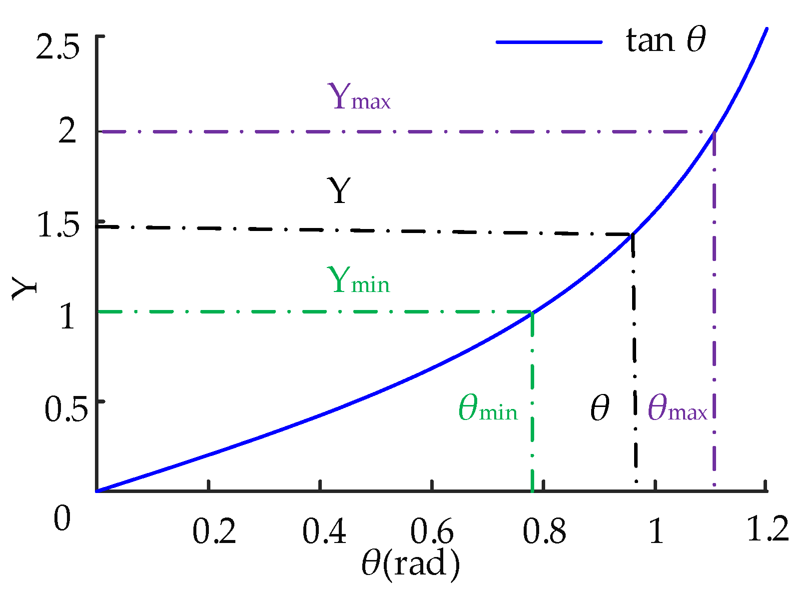
In the actual operating condition, assume that the phase measurement accuracy of the grid-tied inverter is
K under noise interference. From Equation (22), the maximum phase error can be expressed as
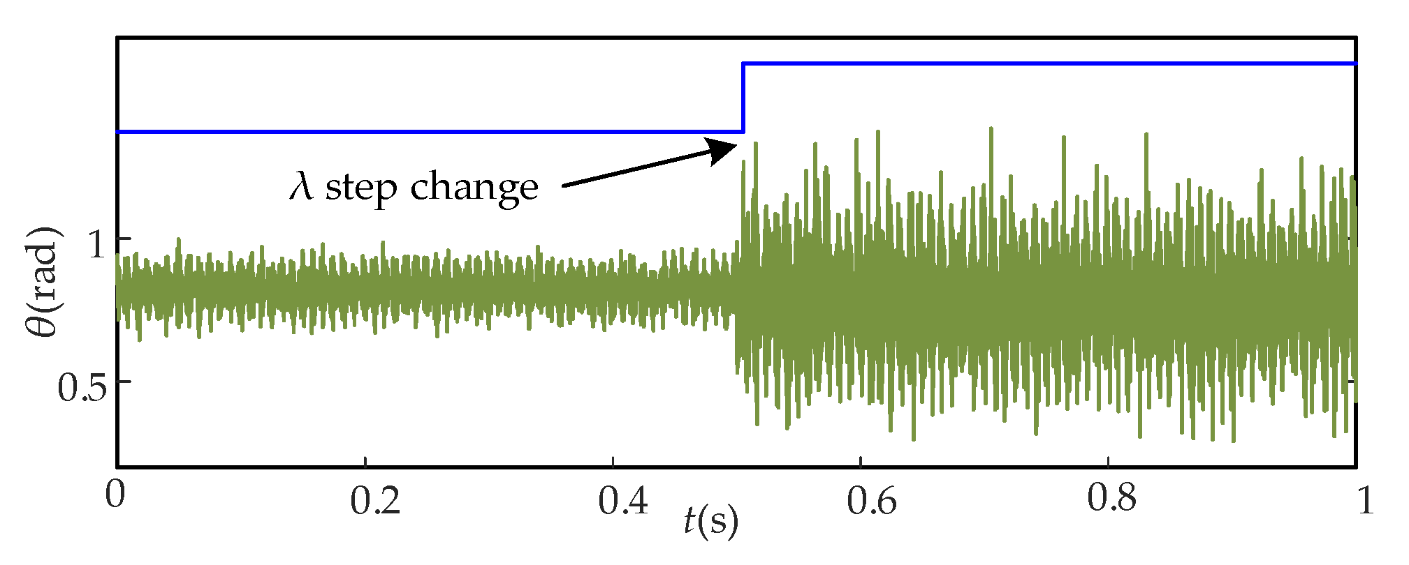
From Equation (24), the relationship between the phase-precision
K and noise ratio λ can be expressed as
If the voltage phase-accuracy is set as K < 2%, the accepted range of the voltage noise ratio agrees with 0 < λ < 8.88%. This means that, if the original voltage magnitude is 100 V and the noise signal value does not exceed 8.88 V, the phase error detected by OPD can meet the accuracy requirement. However, when the high-frequency random noise increases, the phase error is thus larger, which does not meet the requirement of practical accuracy.
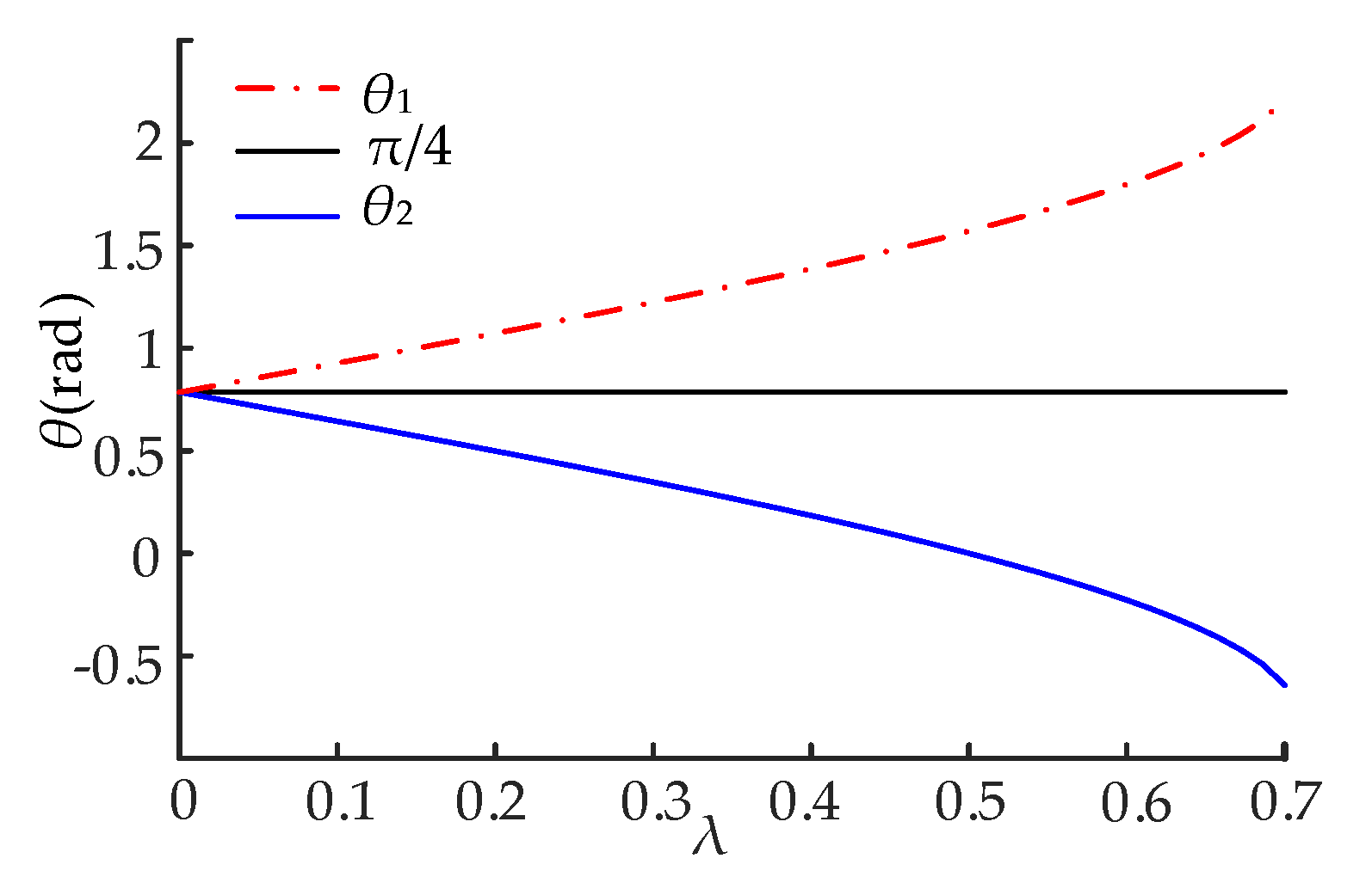
From
Figure 6, if the noise ratio agrees with 0 < λ < 0.1, the initial phase fluctuates at about 45°, which corresponds to the maximum phase error. However, when λ increases, as shown in
Figure 6 and Equation (21),
θ1 and
θ2 are not at the maximum value point.
The bigger λ is, the more θ1 and (or) θ2 deviate from π/4, which will lead to the amplification of Δθmax and other phase errors.
In summary, the conclusions of noise immunity on OPD are as follows:
- (a)
The voltage initial phase detection error is associated with the voltage noise ratio λ. The greater the voltage noise ratio, the greater the phase error. The accuracy of phase detection is greatly affected by the noise value.
- (b)
If the angle between U and d axis is different, OPD has a different noise immunity. When θ ≈ 45°, the phase error is the largest. If θ = 0°, the phase error is the smallest, and the noise interference to phase accuracy is the lowest.
4. Improved OPD
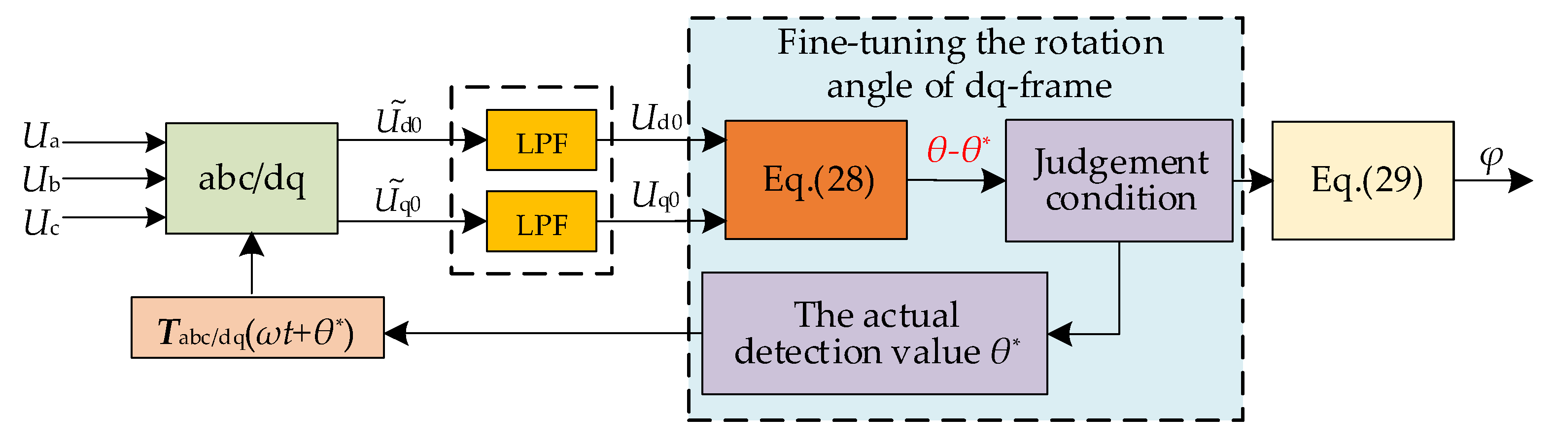
Based on the above, to reduce the phase error, this paper proposes an improved OPD to enhance the noise immunity of OPD. First, the rotation angle of the dq frame is fine-tuned to ensure that the angle between the voltage vector and d axis is always close to 0°, so that the voltage vector could be located in the angle position with the smallest phase error in the dq frame. The noise immunity of OPD could thus be enhanced, and the initial phase detection accuracy can thus be improved. The enhanced OPD algorithm is elaborated in detail below.
From Equation (2) and
Figure 1, it can be seen that, in Clarke’s and Park’s transformation,
ωt is the rotation angle of the dq frame, which determines the rotation speed and relative position relationship between the dq frame and voltage vector
U. For a different initial phase
θ and fixed frequency, the actual detected phase value
θ* has a different phase error (i.e., the closer
θ is to π/4, the larger the detected phase error.). Hence,
ωt +
θ can be used as a simple and effective controlled factor to fine-tune the position of the dq frame.
As shown in
Figure 7,
θ* is the actual detected value of the voltage initial phase under noise interference.
θd0 is the difference between the theoretical initial phase and actual detected value; i.e., the angle between the d
0 axis and voltage
U.
When adding the detected phase value
θ* to the dq coordinate transformation matrix to fine-tune the dq frame,
Tabc/dq (
ωt +
θ*) can thus be rewritten as
After fine-tuning the rotation angle of the dq frame, the voltage DC components in the d
0q
0 frame can thus be expressed as follows:
From Equation (27), the current position of the three-phase voltages could be calculated by
From Equation (28), it can be observed that, under the ideal grid environment (i.e., θ* = θ), the current position of the three-phase voltages calculated by Equation (28) equals that of Equation (6), which shows that the improved OPD algorithm has the same phase detection function as the original OPD.
When the three-phase voltages contain high-frequency random noise, we take θ = π/4 as an example to better illustrate the effect of fine-tuning the rotation angle dq frame to reduce phase detection errors.
First, the relationship between
θ* and
θd0 can be expressed as
From Equation (22), we can see that if
θ equals π/4, the phase error Δ
θ (i.e.,
θd0 ) equals arcsin (λ
1/2) and the actual detected value
θ* equals π/4 – arcsin (λ
1/2); using the original OPD, the current position of the three-phase voltages in the dq frame is shown as
Using Equation (26) to fine-tune the dq frame, the DC components can thus be expressed as
From Equation (31), the current position of the three-phase voltages in the d
0q
0 frame is shown as
From Equations (30) and (32), it can be seen that φd0q0 in Equation (32) is closer to π/4 than φdq in Equation (30), which shows that the improved OPD algorithm can effectively reduce the phase detection error by fine-tuning the rotation angle of the dq frame.
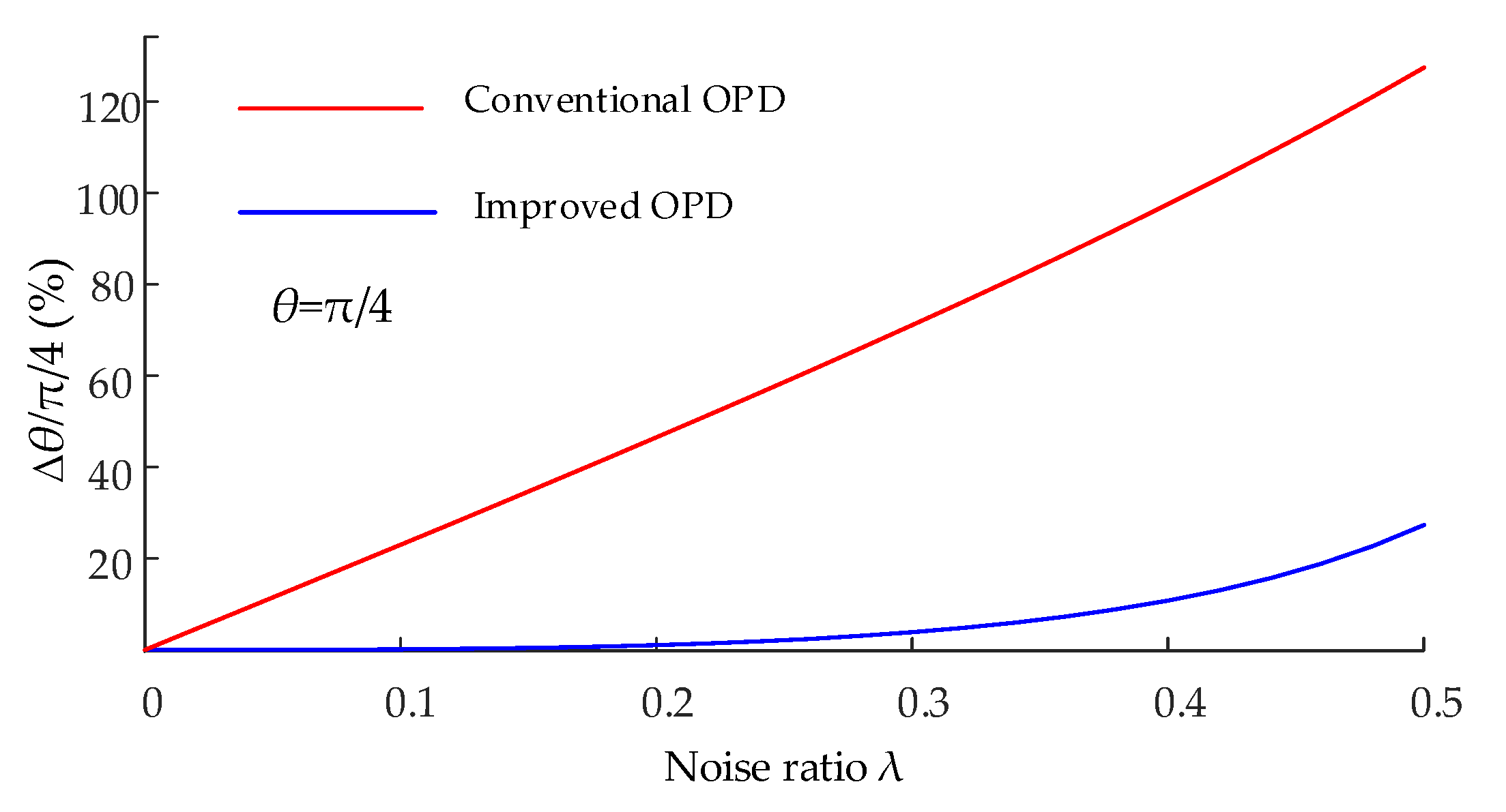
Moreover, the phase error percentage comparison from Equations (30) and (32) is shown in
Figure 8. It can be seen that the proposed improved OPD algorithm can significantly reduce the phase detection error and ensure that the phase detection error is acceptable.
From Equation (32) and
Figure 7, we can see that the larger
θd0, the larger the error calculated by Equation (31) in the d
0q
0 frame. While directly adding the initial phase detection value
θ* into the coordinate transformation matrix without considering the real-time variation of random noise value, which may result in a relatively large angle difference between the d
0 axis and voltage vector
U, the phase detection accuracy of the proposed OPD algorithm will thus be reduced.
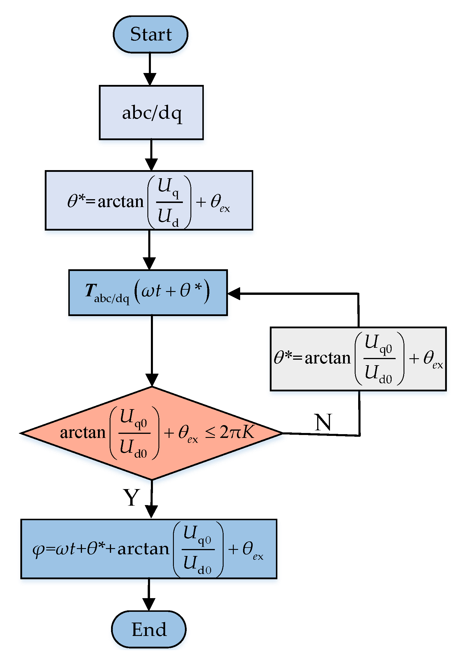
Hence, it is of paramount importance to detect the value of
θd0 in real time to further reduce the phase detection errors. To ensure that the grid voltage vector almost coincides with the d
0 axis in the d
0 q
0 frame, the flow chart of tracking the
θd0 between the voltage vector and d
0 axis and fine-tuning the relative angular position of d
0q
0 frame is shown in
Figure 9.
The judgment condition of angle difference θd0 (i.e., arctan (Uq0/Ud0) + θex) is set as follows:
- (1)
After fine-tuning the rotation angle of the dq frame first, if |arctan(Uq0/Ud0) + θex| ≤ 2πK, it can be seen from Equation (24) that the voltage synchronous phase angle calculated by Equation (30) meets the phase accuracy requirements.
- (2)
Conversely, while the judgment condition is not satisfied (i.e., |arctan (Uq0/Ud0) + θex| > 2πK), the d0q0 frame must be fine-tuned again; arctan (Uq0/Ud0) + θex is simultaneously added to the dq coordinate transformation matrix in Equation (26) for the fine-tuning of the dq frame.
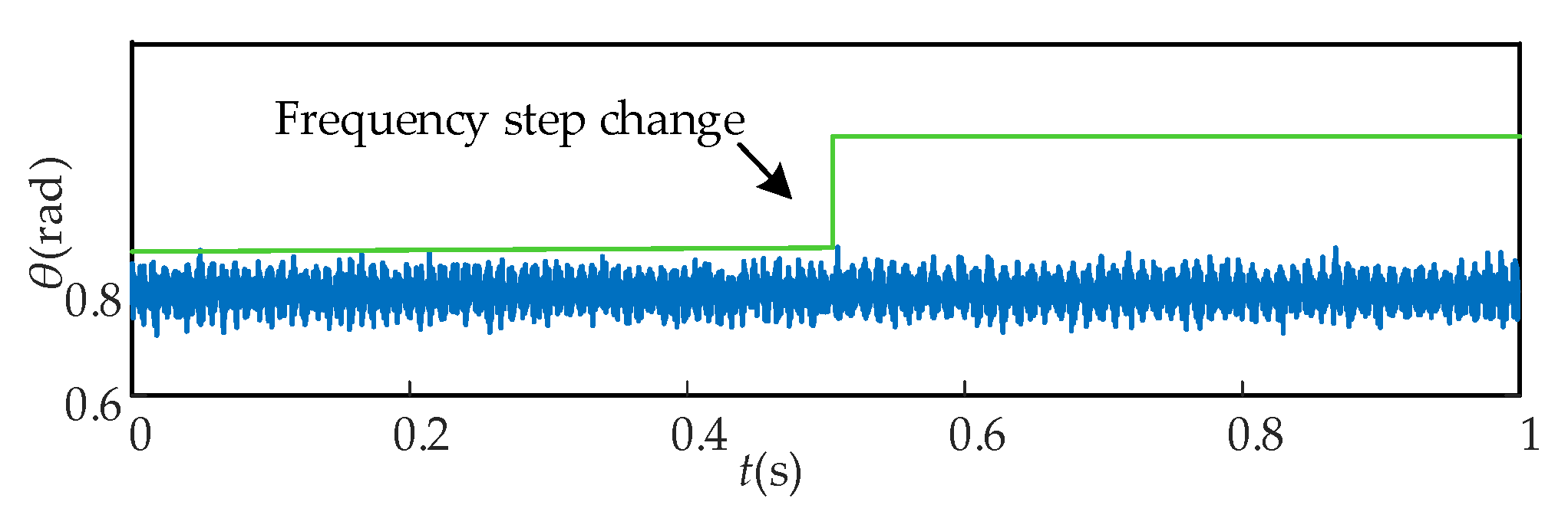
Particularly, when the voltage phase detection requirement for engineering application is higher, even if the included angle of the d axis and voltage vector is close to 0, the phase error may not meet accuracy requirements. Although the enhanced OPD algorithm proposed in this paper can significantly suppress the interference of high-frequency random noise without using LPF, it is difficult to eliminate its influence completely (i.e., 100 % noise suppression).
To further attenuate noise, the high-frequency random noise can be filtered by LPF, however, which will simultaneously sacrifice the dynamic response performance of the control system. The improved OPD algorithm proposed in this paper has achieved the suppression of high-frequency noise for phase measurement accuracy, and the dynamic performance of OPD can thus be enhanced using an LPF with a higher cutoff frequency. The transfer function of the first-order LPF is given as
where
ωf represents the cut-off frequency of LPF.
The scheme of the enhanced OPD algorithm adopting the improved algorithm proposed in this paper is shown in
Figure 10.


