Abstract
The quasi-impedance source inverters/quasi-Z source inverters (Q-ZSIs) have shown improvement to overwhelmed shortcomings of regular voltage-source inverters (VSIs) and current-source inverters (CSIs) in terms of efficiency and buck-boost type operations. The Q-ZSIs encapsulated several significant merits against conventional ZSIs, i.e., realized buck/boost, inversion and power conditioning in a single power stage with improved reliability. The conventional inverters have two major problems; voltage harmonics and boosting capability, which make it impossible to prefer for renewable generation and general-purpose applications such as drive acceleration. This work has proposed a Q-ZSI with five-level six switches coupled inverter. The proposed Q-ZSI has the merits of operation, reduced passive components, higher voltage boosting capability and high efficiency. The modified space vector pulse width modulation (PWM) developed to achieve the desired control on the impedance network and inverter switching states. The proposed PWM integrates the boosting and regular inverter switching state within one sampling period. The PWM has merits such as reduction of coupled inductor size, total harmonic reduction with enhancing of the fundamental voltage profile. In comparison with other multilevel inverters (MLI), it utilizes only half of the power switch and a lower modulation index to attain higher voltage gain. The proposed inverter dealt with photovoltaic (PV) system for the stand-alone load. The proposed boost inverter topology, operating performance and control algorithm is theoretically investigated and validated through MATLAB/Simulink software and experimental upshots. The proposed topology is an attractive solution for the stand-alone and grid-connected system.
1. Introduction
Photovoltaic (PV) energy, extracted through solar cells is a mandatory power generation technology to meet out the global power demand [1]. The most prominent merits in PV generation are reduction of fossil fuel usage, less impact on the environment and reduction in power generation cost [2,3]. The large-scale deviation occurs in the floating power generations that abide by climatic conditions. Unfortunately, the main drawback of the PV array panels is a wide range of drop-in voltage. However, the power electronics devices overcome the voltage drops and floating power generation [4]. The power electronics converter and inverter combinations make PV power transfer an efficient process. The traditional power electronics inverters; voltage-source inverter (VSI), and current-source inverter (CSI) defeats options in the PV power generation with the addition of DC-DC converters. This two-stage power conversion needs more semiconductor switches and passive components; hence they may cause the abrupt disturbance on voltage profile [5]. To prevail over the demerits of traditional inverters, single-stage power conversion is introduce named as Z (impedance) source inverter (ZSI). Impedance networks offer an effective power transformation between the source (input) and an extensive range of loads with high efficiency. However, the ZSI lags in the performance like producing discontinuous nature in the input current; inductors do not withstand high current, and voltage stress on the capacitors [6]. The quasi-Z source has been expected to inherit the merits of the ZSI with reduced passive components, continuous input current, constant DC rail voltage for the inverter, and so on. Before embarking on the investigation of the Z source inverter, it is helpful to look into its evolution. Impedance source topology-based researches have proliferated, from the time it was proposed by Peng et al. in 2003; the variety of alterations and novel Z-source topologies has matured exponentially [7]. In the advancement of ZSI, it finds variety of applications such as; variable-speed electrical drives [8,9], uninterruptible power supply [10], in distributed power generations (such as photovoltaic (PV), fuel cell, and wind, etc.), energy storage system (such as battery and supercapacitor), and electric vehicles [11,12,13]. An earned mark of the Z-source inverter has lost its capability in the form of the input and output voltage ratio profile, switching stress and utilization of higher modulation. These lagging structure needs to be remarked with a quasi (Q)-Z source. The development in the Q-Z source with coupled inductor achieves most compromising effect towards upright of power quality, lower switching dv/dt, better electromagnetic influence, and negligible switching losses [14].
Owing to the advantages and challenges, power electronics researchers have given much interest in impedance-source topology development. The first Z-source was proposed during 2003 (Peng et al.); the variety of alterations, as well as novel topological inventions that have been developed exponentially, are chosen based on the applications and requirements. Concerning power conversion, it is separated into four groups: AC to DC (rectifier), AC to AC (AC voltage regulator), DC to DC (DC chopper), and DC to AC (inverter). This classification is further divided into two-level (conventional VSI) and multi-level DC to AC, AC to AC matrix converters [15] and DC to DC converters in isolated and non-isolated arrangement [16]. Based on the input source (current or voltage), the impedance source topology is further divided into the voltage source and current source Z-source [17]. Besides, considering the impedance components (inductors arrangements), this group can be distributed into coupled inductor (magnetically coupled) or transformer-based [18] and non-transformer (non-magnetically coupled) based [19]. There are selected limitations present in non-magnetically coupled topologies such as lower modulation proportion and lesser, output gain. Therefore, non-transformer topology needs higher boosting inductor and DC-link voltage rating, which may increase the converter switching stress superfluously. Besides, the circuit cost and size for these converters are undesirable. To minimize these concerns, the uses of magnetically coupled inductors or transformers are attractive to increase the operating range and output voltage gain concurrently. The Q-ZSIs proposed in [19,20] offer additional improvement of traditional X shape network topology. Besides the rewards inherited from X shape ZSIs, Q-ZSIs also has its own merits such as continuous current mode operation, reduction of component selection ratings, structured with common DC-rail in the middle of the input and inverter. There are modified Q-ZSI topologies comprehensibly investigated within their improvement to provide continuous input current [21]. Yang et al. propose the current-fed Q-ZSI., including the benefits of the combined buck-boost operation, enhanced reliability, reduced component ratings, as well as single-stage regeneration capability. This topology provides consistency with the input current control and performs better than Q-ZSI.
In the current era, the interests of multilevel inverters (MLIs) have increased than the conventional VSIs, due to their merits [22]. Particularly the development of power semiconductor technology makes it easy to tradeoff the selection of power devices. New MLIs have been recommended in a hybrid approach by involving MOSFETs, IGCTs or GTOs and IGBTs [23,24,25,26,27]. Recently, the interleaved converter topology using coupled-inductors is proposed and extensively applied in low-power claims. These topologies are mostly used to increase the output current with lesser current ripple.
Additionally, the interleaved converter reduces the size of passive components (inductors and capacitors), and the output voltage harmonic profile is considerably increased [28,29,30,31,32,33,34,35,36,37,38,39]. Banaei et al. discussed the switching stress reduction in Z source-based MLI [36]. Alexandre Battiston et al. deliberated the withdrawal of the ripples in the input current with the suitable coupled inductors arrangement [37]. Li et al. proposed the use of the cascading magnetic cells to obtain a high voltage gain [38] and investigated the voltage gain achievement against smaller duty time. Followed by the authors, Lei et al. offered optimized pulse width modulation (PWM) technique with reduction of switching loss, current ripple, low total harmonic distortion (THD) and high boost gain [39]. The space vector PWM is extensively reviewed for impendence sourced VSIs and MLIs [40,41,42,43,44,45,46,47,48,49]. The creation of shoot-through (ST) and placing them in the active switching states, these PWM methods perform better than other carrier-based PWM methods. The ZSI space vector PWM is also studied with two-level MLIs for altering the active and ST switching vector in the space vector diagram for the enhancement of inverter output [44]. However, when connecting a coupled inverter with an impedance network, the PWM methods need to be modified.
Based on this technical background and coupled MLI and control scheme requirements of ZSI, this paper suggests a single-phase MLI coupled inverter topology with five-level output for PV application. This PV tied five-level coupled inverter topology is connecting the modified Q-ZSI with a six-switch coupled inverter, making a single stage DC to AC conversion topology. The proposed Q-ZSI has the merits of operation, namely reduced passive components, voltage boosting capability and high efficiency. The modified space vector PWM is proposed to realize the desired control in impedance network shoot-through and regular inverter switching state to make five-level output. The proposed PWM is integrating the boosting and regular inverter switching state within one sampling period. The PWM has the merits like a reduction of coupled inductor size and triplen harmonic reduction with the enhancement of the fundamental voltage profile.
In comparison with other MLIs, it utilizes only half of the power switch, lower modulation index to obtain high voltage gain. The proposed inverter is simulated and experimentally validated for single phase induction motor load with off-grid fashion. Nevertheless, the proposed inverter topology is a suitable version for both off-grid and on-grid applications.
The paper flow is organized in this way. Section 2 deals with the review of traditional Z-source inverter. The proposed modified Q-impedance converter fed coupled inductor multilevel inverter is explained in Section 3. The modified Space Vector PWM concept and control methods of the proposed inverter are shown in Section 4, Section 5, Section 6 and Section 7 explain the simulation and experimentation, respectively. The conclusion is given in Section 8.
2. Review of Traditional Z-source Inverter
2.1. Review of X-Z Source Topology
Figure 1 illustrates the general impedance-source configuration with the impedance-source network for VSI. The basic Z-source network structure is generalized as a necessary X shaped two-port network using two L and C (linear energy storage elements) (Peng et al. 2003). Perhaps designing different Z-source network configurations to expand the converter performance, non-linear elements (switches, diodes, or/and combination of both) is added in the shape two-port network (Peng et al. 2003).
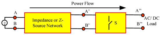
Figure 1.
Impedance source inverter basic block diagram.
According to Figure 2, the impedance-source network has two modes of work. During the mode-1, inverter switch is short-circuited to provide the charging loop for an inductor with input DC source. This state is called the ‘shoot-through (ST) state’. The second mode is the active mode, where energy stored in the inductors is supplied the load via inverter active mode switching. To connect this ST state with regular inverter active switch, there are a variety of modulation methods available. The modulation methods are distributing the ST states equally based on the modulation index of the inverter (Ma). The upper limit of the modulation index is 1-DS. For the maximum boost modulation method, the modulation index is operated in extensive range (Ma ≥ 1); however, the state involves larger (high rating), passive (L and C) elements [8], and correspondingly distributing the active states, the Ma has its maximum Ma ≤ 1–DS [14]. Therefore, VC1 = VC2 = VPL. During this time, high-frequency generation in the active states causes higher frequency ripples, as shown in Figure 2a. According to the characteristics of Z-source inverter boost mode operation, the performance of inductor and capacitor components and DC-link voltage estimation related to input voltage function are shown in Figure 2b. From the characteristics curve, it is understood that the inverter matches the maximum DC-link voltage with the least input voltage. The inductor curve has a challenging dependency with ST time, and the quick capacitance value raise with the decreasing input voltage is essential. Hence, it is noted that passive elements (inductor and capacitor) are carefully chosen based on the input source voltage and power profile. The voltage rating capacitors are required since the voltage across the capacitors is always greater than the input voltage. Similarly, starting current and voltage surge happens because of the enormous inrush input current. Due to the resonance conditions, these surges are not avoidable, and the absence of bidirectional and soft-start capability limits the application for conventional Z-source topology.
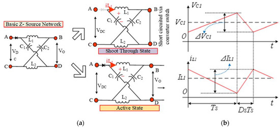
Figure 2.
Impedance source inverter operation: (a) impedance source circuit, shoot through (ST) state, an active state, (b) inductor current and capacitor voltage idealized condition waveforms.
To get improvement in the conventional ZSIs, Q-ZSIs are significantly improved to make use of single-stage power conversions. Considering the circuit operations and boosting, characterizes Q-ZSIs as having similar belongings with conventional ZSIs. Figure 3 illustrates the boost-mode characteristics of ZSIs. The Q-ZSIs differ from the conventional X shape-ZSIs by providing continuous input current through lower capacitor C2 [10]. Regardless of the control strategy of Q-ZSIs, during ST states, the duty ratio is limited concerning inductor rating directly. Hence, there is a possibility of continuous conduction with reduced input inductor current ripples. Besides, Q-ZSI provides the cross conduction switching states to provide the boosting by mutual sharing of inverter switching (top and bottom), which improves the inverter reliability [11]. The Q-ZSI has advantages of reduced component (L and C) ratings, lower switching stress, and continuous current mode operation. The standard ground-sharing option in the Q-ZSI is an additional feature, which is high indeed for PV modules [19]. Even though Q-ZSI has several advantages over conventional X-shape ZSI; it has low DC-link utilization in constant boost operation. To overcome this weakness, Q-ZSIs modified with additional passive components have been proposed [19,20].
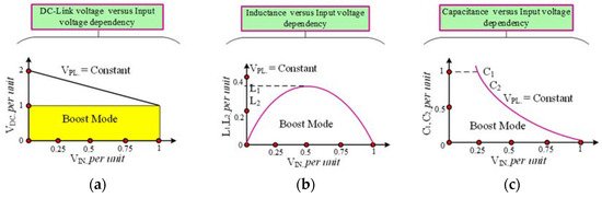
Figure 3.
Boost-mode characteristics of Z-source inverter; (a) DC-link voltage versus input voltage, (b) inductance versus input voltage, and (c) input voltage response versus change in capacitances.
2.2. Different Advanced Z-Source Topologies
Due to the advantages and challenges, power electronics researchers have given much interest in impedance-source topology development. These topologies are categorized into two ways; 1. Transformer based and 2. Without transformer (non-magnetically coupled). Figure 4a–f shows the basic different impedance source topologies.
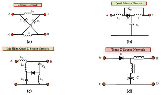
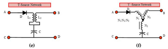
Figure 4.
Different Z-source topologies; (a) Z-source network, (b) Quasi-source network, (c) Modified Quasi-source network, (d) Trans Z-source network, (e) T-source network, (f) Y-source network.
Selected limitations are present in non-magnetically coupled topologies such as low modulation ratio and lesser input-to-output gain. Therefore, this topology needs higher DC-link voltage, which may increase the semiconductors stress needlessly. Besides, the circuit cost and size for these converters are undesirable. Even though the magnetically coupled converters are attractive for their boosting performance, due to the higher DC ripple, the inverter suffers from high harmonics. The disadvantages of magnetically coupled topologies are; (1) raising the shoot-through and magnetizing current while switching; (2) the tightly coupled transformer leads to low leakage impedance; and (3) the need for the snubber circuit is mandatory when the coupling is not fulfilled. Hence, non-magnetic type converters are not highly preferred for PV fed applications [6]. Considering the non-magnetic type converters group, X-shape and Q- impedance converters offer low passive components rating, less duty cycle conversion ratio, and direct conversion. However, it has the poor performance to maintain the input current, reverse blocking capability for the switch, buck-boost operation, absence of bidirectional conversion and direct current control ability. Hence, the paper proposes a coupled inverter connected modified Q-impedance converter to provide single conversion mode power flow operation with multi-level output.
3. Proposed Modified Q- Impedance Converter Fed Coupled Inductor Multilevel Inverter.
The traditional Z source inverters can only allow unidirectional power conversion flow with boosting operation. Nevertheless, the proposed topology is different from the conventional Z source inverter or Q-ZSI family to exchange the diode for bi-directional power flow; the proposed Q-ZSI achieve the boosting capability with single-stage conversion associated with the inverter switching scheme as shown in Figure 5. The first suggestion of a proposed modified Q-impedance network is to obtain the continuous input current is controlled possibility. It consists of the three operating states; (1) active state, (2) shoot-through state, and (3) open-zero states. When related to the conventional X-Z/Q-Z topology, the proposed structure streams the minimum DC voltage on capacitor C2 as well as deliver continuous input current [11,19]. Acknowledging straightforwardness in the control strategy for the proposed quasi-Z-source MLI functions with two operating modes; (1) shoot-through (ST) and, (2) non-shoot-through (NST). In ST mode, among all inverter phase leg, only one leg is conducting for providing ST. In NST mode, all the three leg switches in the inverter are forming the switching states to make a level in MLI. Hence, the inverter is working similar to a standard inverter. The current Z-source inverter switching states are premeditated with two zero states, and six active states. Figure 6 shows the Proposed modified Q-impedance network. The proposed inverter possesses the two open-zero, six active, and one shoot-through states.
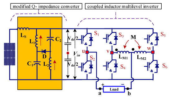
Figure 5.
Proposed modified Q-impedance converter fed coupled inductor multilevel inverter (MLI).
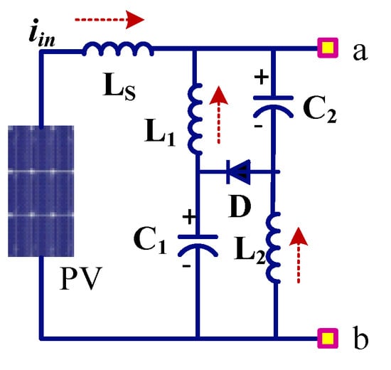
Figure 6.
Proposed modified Q-impedance network.
State-1: Figure 7a shows the active states of the inverter. This mode assumes inductors, L1 and L2 and capacitors, C1 and C2 with chosen identical values as VC1 = VC2 = VC, VL1 = VL2 = VL to maintain a symmetrical output nature. The Kirchhoff’s voltage law is applied in Figure 7a,
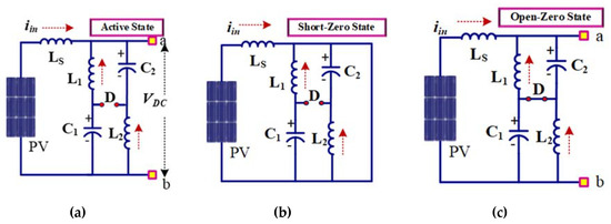
Figure 7.
States of proposed Q- impedance network topology; (a) State-1: active state, (b) State 2: shoot-through states, (c) State-3: open-zero states.
Considering the steady-state average voltage of the inductors in one switching event must be zero. = 0. From Equation (1), the steady-state voltage average of inductors is zero at one single switching period. Hence,
State-2: In this shoot-through state, when any inverter leg is shorted, the PV array voltage is zero, and the diode is off. Thus, the inverter output voltage is zero due to short circuit as shown in Figure 7b, from the equivalent circuit of Figure 7b the KCL equation is given below,
State-3: This is considered to be an open-zero state, where the inverter is switching legs act as an open circuit, and therefore the added capacitor voltages (VC1 and VC2) appear across the Vab. Now, the inductor (L1 and L2) currents flow through diode D1 to charge the capacitors (C1 and C2) as exposed in Figure 7c.
From the circuit operation of the proposed inverter, the total switching period is classified as TA (active state switching time), Tsh (shoot-through state switching time), and Top (open-zero state switching time) within one switching cycle, TA+Tsh+Top =1. Considering any of the three inductors voltage, VL in different states; state-1: VL= Vin-Vout, state-2: VL= Vin, state-3: VL= Vin−2VC.
Since, = 0
From TA+Tsh = 1 − Top
Hence,
The converter DC output voltage boosting (Vboost) has two control degrees of choice (TA and Tsh). Figure 8a shows the graphical understanding between Vboost and input voltage (VPV) concerning duty cycle DA. Here, the operation is split into two modes as (1) Mode-1: without open-zero states, and (2) Mode-2: towards short-zero states to open-zero states.
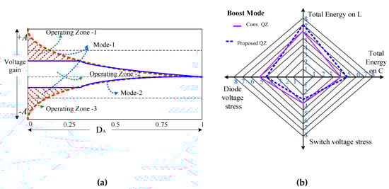
Figure 8.
(a) Converter operation in different modes, Vboost / input voltage (VPV) for duty cycle DA, (b) energy storage capability and voltage stress radar graph of conventional QZ and proposed QZ.
In mode 1 the Top = 0 output voltage depends on the parameter TA = 1 − (Top+Tsh). The entire range of the operation depends on the TA active state switching time. The controlling of the parameter TA decides the boosting capability of the MLI.
In Mode-2, the converter is in shoot-through states, where Top = 1 − TA. Hence the converter provides minimum voltage gain with a specified duty ratio of TA. When converter operation moves from shoot-through states to the open-zero states, the output gain would be situated in the middle of the Mode-1 and Mode-2. The marked red area in Figure 8a shows the mode shift of the converter. Therefore, the converter voltage output can be adjusted to the desired values with two control degrees of freedom Top and TA. Figure 8b shows the radar graph of energy storage capability on C, L, diode voltage stress and switch voltage stress in boost mode for conventional QZ and proposed QZ. It shows the proposed QZ have better energy storage capability and lesser diode and switching voltage stress than conventional QZ.
4. Modes of Operation of Coupled Inductor MLI
The proposed coupled inductor MLI contains a structure having six switches in three legs (u, v and w). The leg v and leg w are connected with identical turns coupled inductor (LM1 and LM2). The ST operation is done through any leg. If the leg u is used for ST, then the switch S1 and S2 are turned ON simultaneously. Since the ST is allowed in any of the MLI legs, the switching reliability is significantly improved. During the Non-ST (active state), the MLI is functioning with either one upper switch and two-lower switches/two-upper switches, and one-lower switch. Hence, during the active state, the inverter is operating with eight modes of operation to produce five-level voltages (−Vdc,−Vdc/2, 0, Vdc/2, and Vdc).
During the regular inverter operating conditions, the boosted voltage is appearing across the inverter and provides pure DC current. For the period of the ST time, the inductor is maintaining its voltage precisely equal to capacitor voltage VC and hence current increases through the inductors leniently and limits the inductor current ripples. The eight modes of operation and their corresponding equivalent circuits of the proposed coupled inductor connected MLI is illustrated in Figure 9.
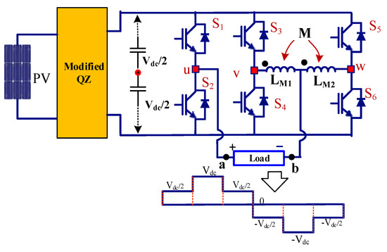
Figure 9.
Coupled inductor MLI.
It is a single-phase circuit with two legs associated with coupled circuits. The quasi fed MLI provides Vpv + VS as input voltage to the coupled inductors (LM1 and LM2). The mutual inductance (M) of the coupled inductors provides the five-level voltage output with a reduction of the switching devices. The level making of the inverter is done through the LM1 and LM2 with the identical sum. The inductor LM1 = LM2 = L is connected between leg v and w. The voltage equation can be expressed as,
where, Vin = input voltage, Vbn = load voltage, and Vwn = w leg voltage
Applying current law of Kirchhoff’s’, the leg current can be written as,
Hence,
The inverter leakage inductance LM1 and LM2 are designed approximately equal to the mutual inductance value; hence leakage inductance equals mutual inductance (L = M). Therefore, the voltage equation on Vbn can be written as,
The voltage output of the inverter can be delivered as,
The different modes of operation of active inverter switching for level making are explained as follows;
Mode-1: During Mode-1, the inverter switches S1, S4, and S6 are turned ON, and S2, S3, and S5 are turned OFF (see Figure 10). Hence, from Equation (12) the load voltage is derived as,
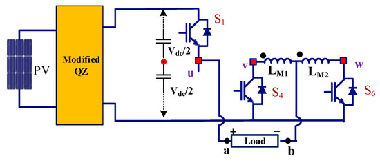
Figure 10.
During mode 1 the inverter switches S1, S4, and S6 are turned ON.
Mode-2: During Mode-2, the inverter switches S1, S4, and S5 are turned ON, and S2, S3, and S6 are turned OFF (see Figure 11). Hence, the inverter produces half of the Vdc (Vs = inverter input voltage). From Equation (12) the load voltage is derived as,
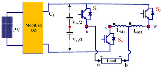
Figure 11.
During Mode-2, the inverter switches S1, S4, and S5 are turned ON.
Mode-3: During the Mode-3, the inverter switches S1, S3, and S6 are turned ON, and S2, S4, and S5 are turned OFF (see Figure 12). Hence, the inverter produces half of the Vdc. From Equation (12) the load voltage is derived as,
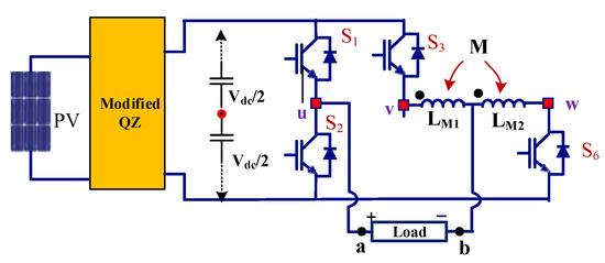
Figure 12.
During mode 3 the inverter switches S1, S3, and S6 are turned ON.
Mode-4: During Mode-4 the inverter switches S1, S3, and S5 (all upper switch) is turned ON, and S2, S4, and S6 (all lower switch) are turn OFF showing in Figure 13. Hence, the inverter produces zero output voltage. From Equation (12) the load voltage is derived as, .
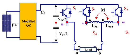
Figure 13.
During Mode-4 the inverter switches S1, S3, and S5 are turned ON.
Mode-5: During Mode-5 the inverter switches S2, S4, and S6 (all lower switch) are turned ON, and S1, S3, and S3 (all upper switch) are turned OFF as shown in Figure 14. Hence, the inverter produces zero output voltage. From Equation (12) the load voltage is derived as, .
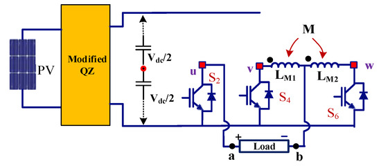
Figure 14.
During mode 5 the inverter switches S2, S4, and S6 are turned ON.
Mode-6: During Mode-6, the inverter switches S2, S4, and S5 are turned ON, and S1, S3, and S6 are turned OFF (see Figure 15). Hence, the inverter produces half of the Vdc. From Equation (12) the load voltage is derived as,
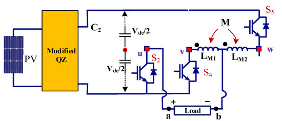
Figure 15.
During mode-6 the inverter switches S2, S4, and S5 are turned ON.
Mode-7: During Mode-7, the inverter switches S2, S3, and S6 are turned ON, and S1, S4, and S5 are turned OFF (see Figure 16). Hence, the inverter produces half of the Vdc. From the Equation.12 the load voltage is derived as,
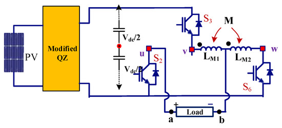
Figure 16.
During Mode-7 the inverter switches S2, S3, and S6 are turned ON.
Mode-8: During Mode-8, the inverter switches S2, S3, and S5 are turned ON, and S1, S4, and S6 are turned OFF (see Figure 17). Hence, the inverter produces full of the Vdc in negative. From Equation (12) the load voltage is derived as,
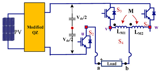
Figure 17.
During Mode-8 the inverter switches S2, S3, and S5 are turned ON.
Table 1 shows the consolidation of the eight modes of operations of the inverter. Of these eight modes, six modes are producing the voltage in different forms between +Vdc to −Vdc. The Mode-4 and Mode-5 are producing the zero voltages, and hence, any one of the modes can be used for zero voltage. Figure 18 illustrates the all mode operation output voltage structure for proposed MLI.

Table 1.
Switching table for the proposed topology.
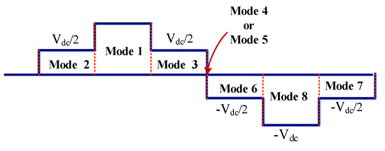
Figure 18.
Output voltage structure for proposed MLI.
5. Modified Space Vector PWM
The Space Vector PWM is a continuous switching PWM technique, which explicitly selects the active and zero states placed within the carrier period [30]. While designing for the boost converter circuitry, the vector-based algorithm possesses the additional switching states which must be imposed to acquire a higher voltage gain in the traditional impedance source inverters. It may lead to impact the switches in the form of stress or failure of a switch [8]. While looking into the traditional strategy, the upper and lower switch combination must be short as the voltage gain may impose distortion on voltage. The proposed space vectors consist of normalized state operation, which generates the voltage gain by operating u, v, w legs upper or lower switches, as shown in Figure 10. The condition ST is incorporated with the regular zero vector operation. The projected control algorithm realizes the least number of switching operations to improve the efficiency of an inverter over one switching cycle, as indicated in Figure 18. The operation time for each period and every switching cycle of the dead time for short-zero as well as open-zero states, should be pre-calculated. The six modes (Mode-1 to Mode-6) of switching states are aligned with active vector and Mode-4, and Mode-5 are placed in zero vector.
In a three-phase balanced system, the voltage equation of Space Vector PWM is predefined as,
Here, Vref is a reference vector (target vector), From Figure 19b in the sector-1, vector Vref can be synthesized as,
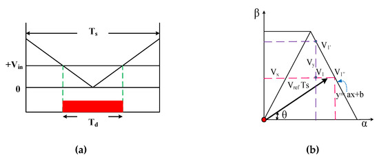
Figure 19.
(a) Dwell time switching states synthesis, (b) proposed control strategy Vref slope.
The V1 and V2 are the adjustment operating vectors at T1 and T2. The Ts is a switching period, and T0 is zero vector time. The pulse period of the active vector is calculated from the below equation when operating in a given switching period Ts.
Hence, the zero-vector time:
The proposed Space Vector PWM strategy is selecting the voltage vector switching sequence, according to Vref. The Vref is the reference vector of output Vab. Hence, the output voltage of the inverter is selected by using switch S1. According to Table 1, when S1 is turned ON, the inverter output voltage Vab is either in positive voltage or zero. Hence the relation is framed between S1 and Vab, for the smooth implementation.
When S1 is turned ON, the Vab ≥ 0 and S1 is low, consequently Vab ≤ 0. Nevertheless, the other switching states should be appropriately combined with S1 to make the desired voltage level of the inverter. In order to select the stable switching states, the dwell time (Td) of the switch is calculated in every switching frequency Ts sampling period. The dwell time concerning inverter DC-link voltage Vin is defined as:
Here, the Vref is related to the sampling period Ts. The ST duty ratio for inverter must be predefined for every switching cycle by adding the ST time within the TS. Figure 19a shows the dwell time control of inverter, and it is related to TS (= 1/fS), and Vin.
To locate the selected switching vector for the Vref, a new method of vector identification is proposed. The strategy is to locate the Vref value and to find out the different switching states in the space vector diagram (SVD) hexagon (see Figure 20). Hence the control strategy is designed in two steps: (1) locate the real and imaginary equivalent of Vref, and (2) find out the control vector within the sector.
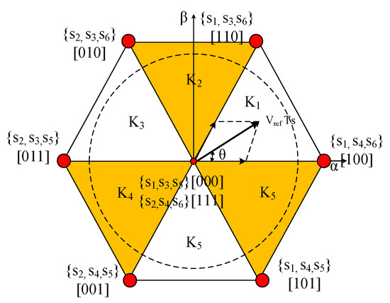
Figure 20.
Space vector diagram and switching table.
Figure 19b represents the proposed control strategy in which, from the Vref slope, the real and imaginary equivalent of Vx and Vy are determined and compared with the targeted switching vector V1 and V1’. Here, when the condition is Vy < a Vx + b, then V1 is selected. Else V1’ is selected. Once this targeting vector is selected, the Td is calculated and then active switching time, ST time and zero switching time is calculated according to the inverter output voltage requirement. Figure 20 represents the overall SVD for the proposed control strategy. Here, the entire active targeted vector is placed inside the SVD sector until the hexagonal boundary. The zero vectors [1, 1, 1] and [0, 0, 0] are placed at the origin. The control switching vector is directly related to the inverter modulation index (ma), where Vin and Vref are related to the inverter output. The maximum inverter control in the linear modulation range is allowed only until Vin [23]. The switching pulse patent of the proposed PWM is prearranged in Figure 21. Once the active and zero states are done, the ST state patent is included in the switching sampling period. The ST state is calculated based on the VPV value. Figure 22 represents the inverter switching pulse. The zero-state sharing ST state and ST time is calculated directly from the following equations:
where B is a boosting factor.
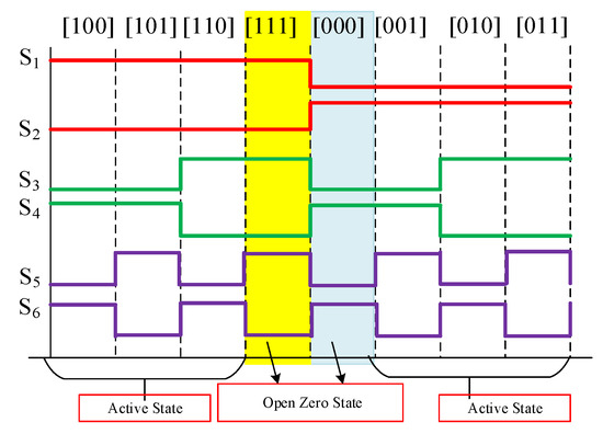
Figure 21.
Space vector PWM algorithm and switching table.
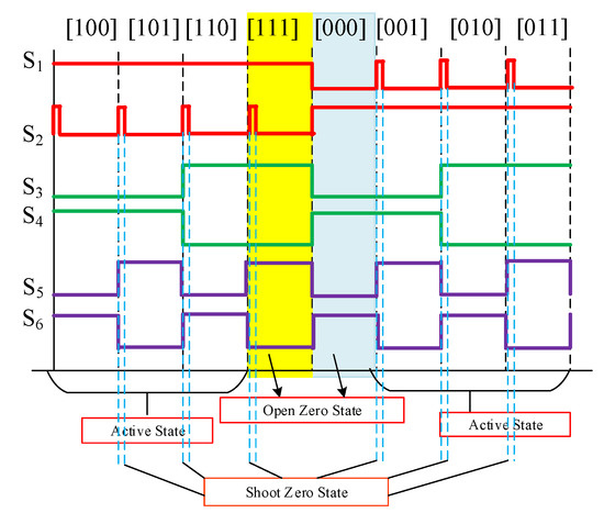
Figure 22.
Proposed impedance source Space vector PWM and switching table.
6. Simulation Result
The PV powered Q-impedance network connected coupled inductor multilevel inverter and its control switching schemes strategy is designed in MATLAB/Simulink software simulation platform (Figure 23). The inverter is powered by 500 Watts peak power PV. The PV module is arranged to get 100 to 120 V to meet the 330 V DC-link voltage of the inverter. The insulation level of the PV array is 1000 W/m2 for 10 s, 800 W/m2 from 10 s to 30 s. The temperature of the PV array is 400°C for 10 s and 300 °C from 10 s onwards. The variation in PV array power input can be overcome by the Perturb and Observe the MPPT algorithm to obtain the constant DC voltage from the PV array. Table 2 shows the simulation parameter for the proposed inverter. The inverter performance is investigated with and without LC filters.
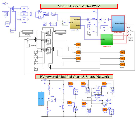
Figure 23.
Simulation diagram of the proposed photovoltaic (PV) powered modified Q-impedance converter fed coupled inductor MLI.
Table 2.
Simulation Parameters.
In order to validate the inverter performance simulation is carried out when the PV input power is kept at 500 W and the input PV voltage, VPV is maintained at 120 V. The impedance network duty ratio (TA and TST) is maintained at 20% to 25% to preserve the inverter input (DC-link) voltage 250 to 350 V. The inverter operation is investigated with their modulation index range ma = 0 to 0.866. The simulation study is carried out for different impedance network duty ratio TST and inverter modulation index range ma. Initially, the inverter is operated with a maximum modulation index of 0.886 with the ST switching time TST of 25%. Figure 24 shows the PWM pulse of inverter switches S1 and S6. The ST time between switch S1 and S2 is represented in Figure 25, in which the 25% switching time is used for ST event, and hence impedance network can boost input PV voltage nearly 290% and achieved 349 V in the output side of the impedance network (DC-link voltage of inverter). During the operation, the voltage of impedance network capacitors VC1 and VC2 shows uniform charging and discharging profile (see Figure 26) along with the uniform inductors current profile ( see Figure 27). Hence, during the ST period, the impedance network can draw the constant current and provide a regulated boost DC-link voltage to the MLI. Figure 28 and Figure 29 illustrates the captured the inverter input DC-link voltage and multi-level output voltage across the load (Vab) respectively. From the results, it can be seen that the 120 V input PV voltage is boosted to 349 V. The inverter load voltage Vab is observed as 247.3 V (RMS). The corresponding Vab voltage THD spectrum is shown in Figure 30 (without filter). Here the inverter voltage THD is observed as 14.15%, which is higher due to the participation of passive elements in the impedance network. Hence the LC filter is connected across the load, and harmonics spectrum is captured (see Figure 31 and Figure 32). The output voltage THD perceived is very less as 2.81%. The inverter load current waveform and its corresponding current THD spectrum are captured and shown in Figure 33a,b. As expected, the current THD is very less (1.7%).
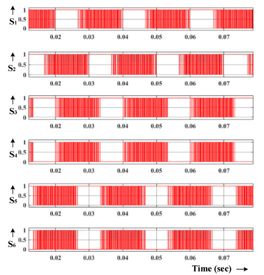
Figure 24.
Modified Q- impedance converter fed coupled inductor MLI.
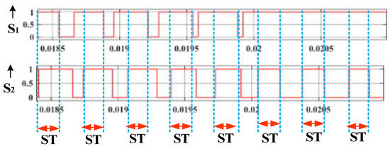
Figure 25.
ST state representations of S1 and S2.
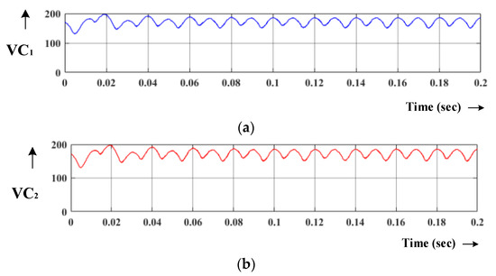
Figure 26.
Voltage waveform of impedance network capacitors at TST = 25%; (a) VC1, (b) VC2.
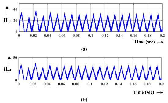
Figure 27.
Current waveform of impedance network inductor at TST = 25%; (a) L1, (b) L2.
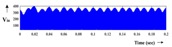
Figure 28.
Inverter DC-link voltage at TST = 25%.
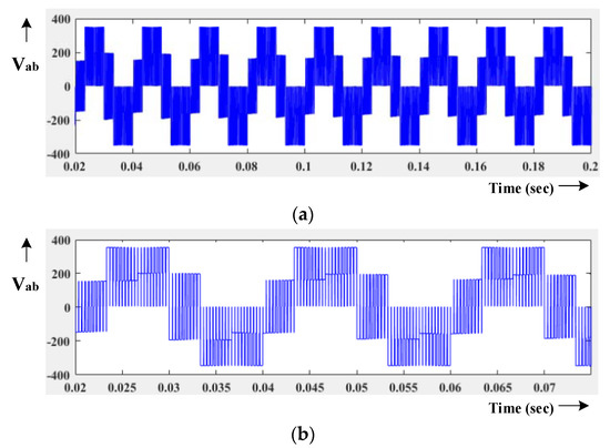
Figure 29.
(a) Inverter output voltage at TST = 25% without filter, (b) zoomed view of the inverter output voltage at TST = 25% without a filter.
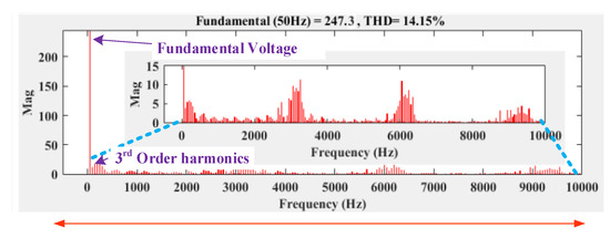
Figure 30.
THD profile of inverter output voltage when TST = 25% without a filter.
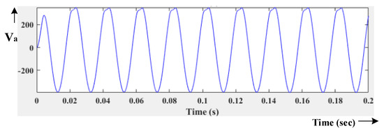
Figure 31.
Inverter output current at TST = 25% with filter.
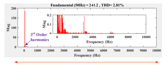
Figure 32.
THD profile of inverter output voltage at TST = 25% with filter.
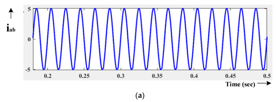
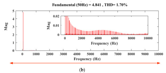
Figure 33.
(a) Inverter output current at TST = 25%, (b) THD profile of inverter output current at TST = 25%.
Next, the simulation study is extended to TST = 20% with 0.866 ma. In this operating condition, the impedance network has boosted the input PV voltage to nearly 230% and maintaining the inverter DC-link voltage at 280 V. The observed DC-link voltage and impedance network capacitor voltages are shown in Figure 34 and Figure 35. While operating the inverter with a modulation index value of ma = 0.866, the inverter has produced the output voltage of 197.23 V, as shown in Figure 36. The inverter output voltage THD is shown in Figure 37. Using LC filter in the inverter output terminal similar to 25% TST performance, the voltage THD for TST = 20% is maintained lesser value as 2.71%. Correspondingly the current THD is observed as 1.70%. In order to validate the higher ST switching time, the simulation is extended to TST = 30% with different modulation indices. During this operating condition, the impedance network passive elements are utilized fully and hence the voltage THD triumphs to a higher value. Figure 38 and Figure 39 illustrates the inverter output voltage and its corresponding voltage THD (without LC filter) for ma = 0.6. Though the inverter voltage is preserved as 292V nearly, the voltage THD is poor. Table 3 and Table 4 illustrates inverter voltage and its THD performances for ma = 0.86 and ma = 0.6 through different duty ratio from 10% to 30% without and with an LC filter, respectively.
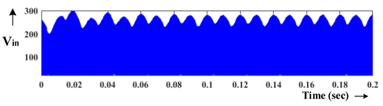
Figure 34.
Inverter DC-link voltage at TST = 20%.
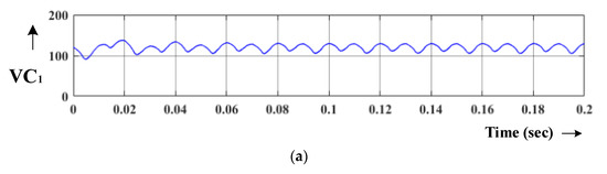
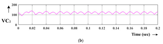
Figure 35.
Voltage waveform of impedance network capacitors at TST = 20%; (a) VC1, (b) VC2.
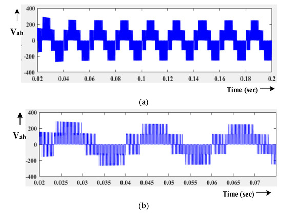
Figure 36.
(a) Inverter output voltage at TST = 25% without filter, (b) zoomed view of inverter output voltage at TST = 25% without filter.
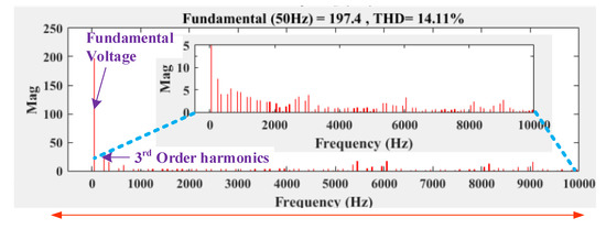
Figure 37.
THD profile of inverter output voltage at TST = 25% without a filter.
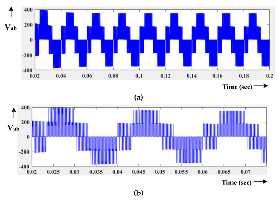
Figure 38.
(a) Inverter output voltage at TST = 30% without filter, (b) zoomed view of the inverter output voltage at TST = 30% without a filter.
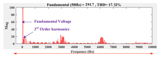
Figure 39.
THD profile of inverter output voltage at TST = 30%.
Table 3.
Detailed simulation results for different duty ratio without an LC filter at ma = 0.86 and 0.6.
Table 4.
Detailed simulation results for different duty ratio with an LC filter at ma = 0.86 and 0.6.
From the tabulated results, it could be seen that DC-link voltage has a linear variation with DST. However, the THD of the inverter voltage increases when increasing the DST. For any value less than or equivalent to DST 25% in any modulation index, the inverter provides a wide range of voltage variation with better voltage and current THD performance.
7. Experimental Result
The proposed PV powered Q-impedance fed coupled inductor multilevel inverter experimental setup was built using six MOSFETs IRF640. The switching signals were associated with the MLI through gate driver TLP250. The switching frequency, fs of the inverter is fixed 10 kHz for the 50 Hz inverter output. The 500 W PV module is arranged to get 100 to 120 V to meet 330 V DC-link voltage to the MLI. The RL load (resistance = 10 Ω and inductance = 5 mH) and LC filter (inductance and capacitor values of 2.5 mH, and 50 µF respectively) are used in the inverter output terminal.
Figure 40 shows the experimental setup photograph. The impedance network and other parameters used for the inverter are the same as the simulation model given in Table 2. The control switching scheme strategy is designed in PIC16F778A microcontroller, and the collaborative results are shown in keyset two channels digital signal oscilloscope (DSO).
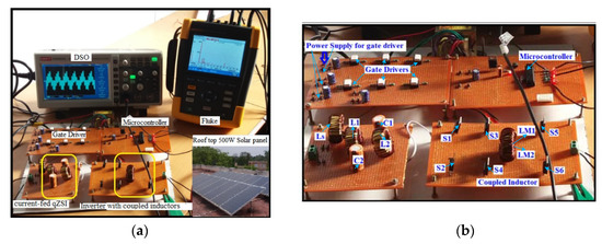
Figure 40.
Experimental setup; (a) overall laboratory-scale 500 W PV powered modified Q-impedance fed coupled inductor MLI, (b) modified Q-impedance fed coupled inductor MLI.
The experimentation is carried out for the 500W constant PV power for 100 V and 5 amps current. The impedance network duty ratio is maintained at 25% with the aim of inverter constant DC-link voltage 300V. The inverter operation is investigated with its modulation index range ma = 0 to 0.866. Initially, the inverter is operated with maximum ma = 0.886, and the results are captured. Figure 41 shows the PWM pulse of inverter switches S1 and S2. The ST time between switch S1 and S2 is represented, in which the 25% switching time is used for ST event, and hence impedance network can generate 300% boosting to maintain the DC-link voltage. Figure 42a shows the current waveform of impedance network inductor L1 and L2. Figure 42b displays the voltage waveform of impedance network capacitors C1 and C2. The voltage profile across the impedance network capacitors VC1 and VC2 are indicating that variation in the VC1 and VC2 are identical. It can be observed that voltages VC1 and VC2 are equally charging the voltage since both are connected in series. Hence the proposed impedance network can provide regulated DC-link voltage to the inverter. Figure 43a,b shows the inverter output voltage (without filters) and input voltage waveform at ma = 0.866. The results show the measured five-level inverter voltage with symmetrical set output voltage 0V, ± 125 V, ± 250 V. The THD value of load voltage is captured using power analyzer and is found to be about 17.1% (shown in Figure 44). The same experimentation is investigated further with filter, and the results are captured. Figure 45a,b shows the filtered output load and load current respectively, where the current and voltage are maintaining their THD lesser as 3.1% and 1.4% respectively (Figure 46a,b).
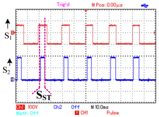
Figure 41.
PWM pulse generation (S1 and S2).
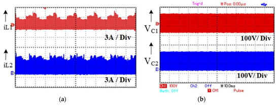
Figure 42.
Experimental result; (a) boost inductor current (iL1 and iL2), (b) voltage waveform of impedance network capacitors C1 and C2.
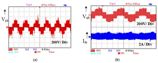
Figure 43.
Experimental result; (a) inverter five-level output voltage, (b) quasi Z-source inverter input current waveform.
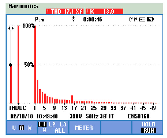
Figure 44.
Experimental voltage THD spectrum without a filter.
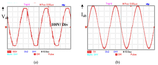
Figure 45.
Experimental result; (a) inverter output voltage with filter, (b) inverter output current waveform with filter.
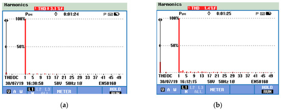
Figure 46.
Experimental result; (a) voltage THD spectrum with filter, (b) current THD spectrum with filter.
To understand the inverter input current control, the duty cycle is varied to 25% and 30%, and results are observed. As expected, the inverter is maintaining the input current regulation at 25% DST. However, when DST is applied to 30%, the impedance network starts losing its input current regulation. Figure 47 illustrates the output voltage of MLI and impedance input current at 25% and 30% DST. From the results, it could be seen that the input PV voltage is boosted via the impedance network to achieve the load voltage of 230 V peak to peak. The DC-link voltage is regulated with a minor ripple of 3%, and hence inverter can maintain its half symmetry and THD of the output voltage is perceived as less. The interesting point to notice at this stage is that the inverter can draw constant current since the impedance network input inductor LS limits the current. The proposed inverter reliability study is conducted for different inverter operating conditions. Table 5 illustrations the switching loss, inverter efficiency, and THD of the proposed inverter for DST 10% to 30% and ma = 0.86. From the results, it can seem that the efficiency is higher in all duty cycle. During the 10% DST, the inverter efficiency is about 95.68%. However, there is a small dip inefficiency at 20% and 30% duty cycle.
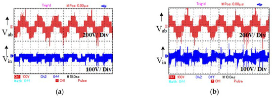
Figure 47.
Experimental result; (a) quasi Z-source coupled MLI output voltage and input current at DST = 25%, (b) quasi Z-source coupled MLI output voltage and input current at DST = 30%.
Table 5.
Switching loss, inverter efficiency, and THD of the proposed inverter for ma = 0.86 and fs = 10 kHz concerning DST from 10% to 30%.
The proposed inverter topology, in comparison with other reported topologies for the gain accomplishments, are deliberated in Table 6. In terms of passive element usage and maximum achievable voltage gain, the proposed topology is better than topology presented in [45,46,47]. By comparing the proposed topology with inverter proposed in [36], though the proposed inverter used one extra inductor, the voltage gain is high (3 times). Figure 48 illustrates the passive components rating, cost, boosting, and THD comparisons with other similar topologies [31,39,48]. The proposed inverter topology attains fewer passive elements usage, higher voltage gain conversion and better voltage THD than [31,39,48]. Thus, the proposed inverter topology presents its efficiency and suitability for PV standalone and grid-connected systems.
Table 6.
Switching loss, inverter efficiency, and THD of the proposed inverter for ma = 0.86 and fs = 10 kHz concerning DST from 10% to 30%.
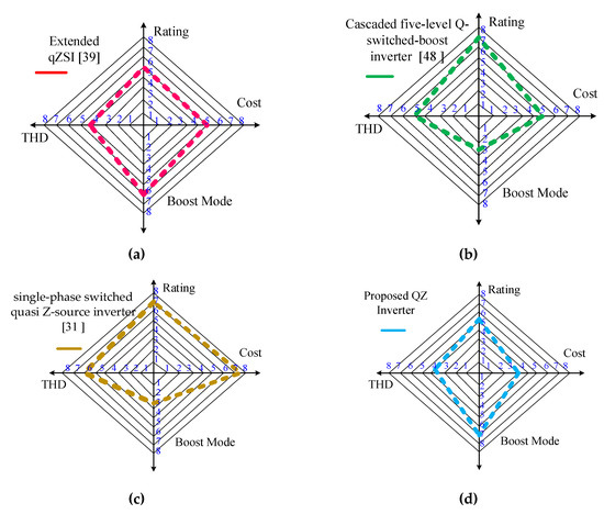
Figure 48.
Passive components rating, cost, boosting, and THD comparisons; (a) Reference [39], (b), Reference [41], (c) Reference [39], (d) proposed QZ Inverter.
8. Conclusions
The proposed Q-source MLI coupled inverter ZSI is a combination of modified Q-source impedance network with six switches coupled inductor connected single-phase five-level MLI. The quasi-Z source coupled inductors MLI tied photovoltaic system with modified space vector PWM produces a maximum voltage gain of 140%. The suggested topology generates the five-level output voltage with the higher voltage gain (maximum voltage gains of 310%) with exceptionally low voltage and current THD. Besides, the proposed MLI reduces the switching stress on the inverter for all the duty cycles in the switching algorithm, when increasing the duty cycle, the boost factor also increases. The proposed quasi Q-ZSI has the merits of operation such as reliability, reduced passive components, voltage boosting capability and reduction in switching stress. The modified space vector PWM is proposed to integrate the boosting and regular inverter switching state within one sampling period.
In comparison with other MLI, it utilizes only half of the power switch, lower modulation index to acquire high voltage gain. The performance of the proposed boost MLI topology and control algorithm is theoretically investigated and validated through MATLAB/Simulink software and experimental upshots. The proposed topology is an attractive solution for stand-alone and grid-connected PV applications.
Author Contributions
M.P. and B.C. have developed the proposed research concept, and they both are involved in studying the execution and implementation with statistical software by collecting information from the real environment and developed the simulation model for the same. S.K.V., S.P., L.M.-P., Y.A. shared their expertise and validation examinations to confirm the concept theoretically with the obtained numerical results for its validation of the proposal. All authors are to frame the final version of the manuscript as a full. Moreover, all authors involved in validating and to make the article error-free technical outcome for the set investigation work.
Funding
No source of funding for this research activity.
Conflicts of Interest
The authors declare no conflict of interest.
References
- Nayak, P.K.; Mahesh, S.; Snaith, H.J.; Cohen, D. Photovoltaic solar cell technologies: Analyzing state of the art. Nat. Rev. Mater. 2019, 4, 269–285. [Google Scholar] [CrossRef]
- Heydari Gharahcheshmeh, M.; Tavakoli, M.M.; Gleason, E.F.; Robinson, M.T.; Kong, J.; Gleason, K.K. Tuning, optimization, and perovskite solar cell device integration of ultrathin poly (3,4-ethylene dioxythiophene) films via a single-step all-dry process. Sci. Adv. 2019, 5, 0414. [Google Scholar] [CrossRef] [PubMed]
- Cui, Y.; Yao, H.; Zhang, J.; Zhang, T.; Wang, Y.; Hong, L.; Xian, K.; Xu, B.; Zhang, S.; Peng, J.; et al. Over 16% efficiency organic photovoltaic cells enabled by a chlorinated acceptor with increased open-circuit voltages. Nat. Commun. 2019, 10, 2515. [Google Scholar] [CrossRef] [PubMed]
- Kavya Santhoshi, B.; Mohana Sundaram, K.; Padmanaban, S.; Holm-Nielsen, J.B. Critical Review of PV Grid-Tied Inverters. Energies 2019, 12, 1921. [Google Scholar] [CrossRef]
- Ellabban; Abu-Rub, H. Z-source Inverter: Topology Improvements Review. IEEE Ind. Electron. Mag. 2016, 10, 6–24. [Google Scholar] [CrossRef]
- Siwakoti, Y.P.; Peng, F.Z.; Blaabjerg, F.; Loh, P.C. Impedance-Source Networks for Electric Power Conversion Part I: A Topological Review. IEEE Trans. Power Electron. 2015, 30, 699–716. [Google Scholar] [CrossRef]
- Peng, F.Z. Z-source inverter. IEEE Trans. Ind. Appl. 2003, 39, 504–510. [Google Scholar] [CrossRef]
- Peng, F.Z.; Yuan, X.; Fang, X.; Qian, Z. Z-source inverter for adjustable speed drives. IEEE Trans. Power Electron. 2013, 1, 33–35. [Google Scholar] [CrossRef]
- Peng, F.Z.; Joseph, A.; Wang, J.; Shen, M.; Chen, Z.L.; Pan, E.; Rivera, O.; Huang, Y. Z-source inverter for motor drives. IEEE Trans. Power Electron. 2005, 20, 857–863. [Google Scholar] [CrossRef]
- Zhou, Z.J.; Zhang, X.; Xu, P.; Shen, W.X. Single-phase uninterruptible power supply based on Z-source inverter. IEEE Trans. Ind.Electron. 2008, 55, 2997–3004. [Google Scholar] [CrossRef]
- Liu, J.; Jiang, S.; Cao, D.; Peng, F.Z. A digital current control of quasi-Z-source inverter with battery. IEEE Trans. Ind. Informat. 2013, 9, 928–936. [Google Scholar] [CrossRef]
- Peng, F.Z.; Shen, M.; Holland, K. Application of Z-source inverter for traction drive of fuel cell-battery hybrid electric vehicles. IEEE Trans. Power Electron. 2007, 22, 1054–1061. [Google Scholar] [CrossRef]
- Zhang, Y.; Shi, J.; Fu, C.; Zhang, W.; Wang, P.; Li, J. An Enhanced Hybrid Switching-Frequency Modulation Strategy for Fuel Cell Vehicle Three-Level DC-DC Converters with Quasi-Z Source. Energies 2018, 11, 1026. [Google Scholar] [CrossRef]
- Loh, P.C.; Gao, F.; Blaabjerg, F.; Feng, S.Y.C.; Soon, N.J. Pulsewidth-modulated Z-source neutral-point-clamped inverter. IEEE Trans. Ind. Appl. 2007, 43, 1295–1308. [Google Scholar] [CrossRef]
- Ge, B.; Li, Q.; Qian, W.; Peng, F.Z. A family of Z-source matrix converters. IEEE Trans. Ind. Electron. 2012, 59, 35–46. [Google Scholar] [CrossRef]
- Vinnikov, D.; Roasto, I. Quasi-Z-source-based isolated DC/DC converters for distributed power generation. IEEE Trans. Ind. Electron. 2011, 58, 192–201. [Google Scholar] [CrossRef]
- Siwakoti, Y.P.; Loh, P.C.; Blaabjerg, F.; Town, G. Y-source impedance network. IEEE Trans. Power Electron. 2014, 29, 3250–3254. [Google Scholar] [CrossRef]
- Ge, B.; Abu-Rub, H.; Peng, F.Z.; Li, Q.; de Almeida, A.T.; Ferreira, F.J.T.E.; Sun, D.; Liu, Y. An energy stored quasi-Z-source inverter for application to photovoltaic power system. IEEE Trans. Ind. Electron. 2013, 60, 4468–4481. [Google Scholar] [CrossRef]
- Yang, S.; Peng, F.Z.; Lei, Q.; Inoshita, R.; Qian, Z. Current-Fed Quasi-Z-Source Inverter with Voltage Buck. IEEE Trans. Ind. Appl. 2011, 47, 882–892. [Google Scholar] [CrossRef]
- Chub, A.; Vinnikov, D.; Liivik, E.; Jalakas, T. Multiphase Quasi-Z-Source DC–DC Converters for Residential Distributed Generation Systems. IEEE Trans. Ind. Electron. 2018, 65, 8361–8371. [Google Scholar] [CrossRef]
- Lei, Q.; Peng, F.Z. Space Vector Pulse width Amplitude Modulation for a Buck–Boost Voltage/Current Source Inverter. IEEE Trans. Power Electron. 2014, 29, 266–274. [Google Scholar] [CrossRef]
- Bharatiraja, C.; Jeevananthan, S.; Munda, J.L.; Latha, R. Improved SVPWM vector selection approaches in OVM region to reduce common-mode voltage for three-level neutral point clamped inverter. Int. J. Electron. Power Energy Syst. 2016, 79, 285–297. [Google Scholar] [CrossRef]
- Manjrekar, M.D.; Steimer, P.K.; Lipo, T.A. Hybrid multilevel power conversion system: A competitive solution for high-power applications. IEEE Trans. Ind. Appl. 2000, 36, 834–841. [Google Scholar] [CrossRef]
- Barbosa, P.; Steimer, P.; Steinke, J.; Meysenc, L.; Winkelnkemper, M.; Celanovic, N. Active neutral-point-clamped multilevel converters. In Proceedings of the Power Electronics Specialists Conference, Recife, Brazil, 16 June 2005; pp. 2296–2301. [Google Scholar]
- Malinowski, M.; Gopakumar, K.; Rodriguez, J.; Perez, M.A. A survey on cascaded multilevel inverters. IEEE Trans. Ind. Electron. 2010, 57, 2197–2206. [Google Scholar] [CrossRef]
- Ruiz-Caballero, D.A.; Ramos-Astudillo, R.M.; Mussa, S.A.; Heldwein, M.L. Symmetrical hybrid multilevel DC-AC converters with reduced number of insulated dc supplies. IEEE Trans. Ind. Electron. 2010, 57, 2307–2314. [Google Scholar] [CrossRef]
- Abdelhakim, A.; Blaabjerg, F.; Mattavelli, P. Modulation Schemes of the Three-Phase Impedance Source Inverters—Part I: Classification and Review. IEEE Trans. Ind. Electron. 2018, 65, 6309–6320. [Google Scholar] [CrossRef]
- Salmon, J.; Ewanchuk, J.; Knight, A.M. PWM inverters using split-wound coupled inductors. IEEE Trans. Ind. Appl. 2009, 45, 2001–2009. [Google Scholar] [CrossRef]
- Ueda, F.; Matsui, K.; Asao, M.; Tsuboi, K. Parallel-connections of pulse width modulated inverters using current sharing reactors. IEEE Trans. Power Electron. 1995, 10, 673–679. [Google Scholar] [CrossRef]
- Bharatiraja, C.; Padmanaban, S.; Siano, P.; Leonowicz, Z.; Iqbal, A. A hexagonal hysteresis space vector current controller for single Z-source network multilevel inverter with capacitor balancing. In Proceedings of the IEEE International Conference on Environment and Electrical Engineering and 2017 IEEE Industrial and Commercial Power Systems Europe, Milan, Italy, 6–9 June 2017. [Google Scholar]
- Nguyen, M.K.; Lim, Y.C.; Park, S.J. Improved trans-Z-source inverter with continuous input current and boost inversion capability. IEEE Trans. Power Electron. 2010, 28, 4500–4510. [Google Scholar] [CrossRef]
- Bharatiraja, C.; Sanjeevikumar, P.; Mahesh; Swathimala, A.S.; Raghu, S. Analysis, design and investigation on a new single-phase switched quasi Z-source inverter for photovoltaic application. Int. J. Power Electron. Drive Syst. 2017, 8, 853–860. [Google Scholar]
- Banaei, M.R.; Dehghanzadeh, A.R.; Salary, E.; Khounjahan, H.; Alizadeh, R. Z-source-based multilevel inverter with reduction of switches. IET Power Electron. 2011, 5, 385–392. [Google Scholar] [CrossRef]
- Battiston, A.; Miliani, E.-H.; Pierfederici, S.; Meibody-Tabar, F. A novel quasi-z-source inverter topology with special coupled inductors for input current ripples cancellation. IEEE Trans. Power Electron. 2015, 31, 2409–2416. [Google Scholar] [CrossRef]
- Li, D.; Loh, P.C.; Zhu, M.; Gao, F.; Blaabjerg, F. Cascaded multicell trans-Z-source inverters. IEEE Trans. Power Electron. 2013, 28, 826–835. [Google Scholar]
- Qin, L.; Dong, C.; Fang, Z.P. Novel loss and harmonic minimized vector modulation for a current-fed quasi-z-source inverter in HEV motor drive application. IEEE Trans. Power Electron. 2013, 29, 1344–1357. [Google Scholar] [CrossRef]
- Bharatiraja, C.; Jeevananthan, S.; Latha, R. Vector Selection Approach-based Hexagonal Hysteresis Space Vector Current Controller for a Three-phase Diode Clamped MLI with Capacitor Voltage Balancing. IET Power Electron. 2016, 9, 1350–1361. [Google Scholar] [CrossRef]
- Bharatiraja, C.; Munda, J.L. Simplified SVPWM for Z Source T-NPC-MLI Including Neutral Point Balancing. In Proceedings of the 4th IEEE Symposium on Computer Applications & Industrial Electronics (ISCAIE2016), Penang, Malaysia, 30–31 May 2016. [Google Scholar]
- Banaei, M.R.; Dehghanzadeh, A.; Oskouei, A.B. Extended switching algorithms based space vector control for five-level quasi-Z-source inverter with coupled inductors. IET Power Electron. 2014, 7, 1509–1518. [Google Scholar] [CrossRef]
- Kumar Gupta, A.; Khambadkone, A.M. A space vector modulation scheme to reduce common mode voltage for cascaded multilevel inverters. IEEE Trans. Ind. Electron. 2007, 22, 1672–1681. [Google Scholar]
- Li, Q.; Wolfs, P.A. review of the single phase photovoltaic module integrated converter topologies with three different dc link configuration. IEEE Trans. Power Electron. 2008, 23, 1320–1333. [Google Scholar]
- Liang, Y.; Liu, B.G.; Abu-Rub, H. Investigation on pulse-width amplitude modulation-based single-phase quasi-Z-source photovoltaic inverter. IET Power Electron. 2017, 10, 1810–1818. [Google Scholar] [CrossRef]
- Tariq, M.; Iqbal, M.T.; Meraj, M.; Iqbal, A.; Maswood, A.I.; Bharatiraja, C. Design of a proportional resonant controller for packed U cell 5 level inverter for grid-connected applications. In Proceedings of the 2016 IEEE International Conference on Power Electronics, Drives and Energy Systems (PEDES), Trivandrum, India, 14–17 December 2016. [Google Scholar]
- Kitson, J.; McNeill, N. A High Efficiency Voltage-Fed Quasi Z-Source Inverter with Discontinuous Input Current Using Super-Junction MOSFETs. In Proceedings of the 8th IET International Conference on Power Electronics, Machines and Drives (PEMD), Glasgow, UK, 19–21 April 2016. [Google Scholar]
- Liu, H.; Li, F.A. Novel High Step-up Converter with a Quasi Active Switched-Inductor Structure for Renewable Energy Systems. IEEE Trans. Power Electron. 2016, 31, 5030–5039. [Google Scholar] [CrossRef]
- Shults, T.E.; Husev, O.; Blaabjerg, F.; Roncero-Clemente, C.; Romero-Cadaval, E.; Vinnikov, D. Novel Space Vector Pulsewidth Modulation Strategies for Single-Phase Three-Level NPC Impedance-Source Inverters. IEEE Trans. Power Electron. 2019, 34, 4820–4830. [Google Scholar] [CrossRef]
- Ho, A.V.; Chun, T.W. A Buck-Boost Multilevel Inverter for PV Systems in Smart Cities. Industrial Networks and Intelligent Systems. Springer Int. Pub. 2018, 295–306. [Google Scholar] [CrossRef]
- Tran, T.T.; Nguyen, M.K. Cascaded five-level quasi-switched-boost inverter for single-phase grid-connected system. IET Power Electron. 2017, 10, 1896–1903. [Google Scholar] [CrossRef]
- Aly, M.; Ahmed, E.M.; Shoyama, M. Thermal Stresses Relief Carrier-Based PWM Strategy for Single-Phase Multilevel Inverters. IEEE Trans. Power Electron. 2017, 32, 9376–9388. [Google Scholar] [CrossRef]


© 2020 by the authors. Licensee MDPI, Basel, Switzerland. This article is an open access article distributed under the terms and conditions of the Creative Commons Attribution (CC BY) license (http://creativecommons.org/licenses/by/4.0/).