1. Introduction
The effective carrier lifetime of a silicon wafer is an important parameter in evaluating the material performance of a crystalline silicon solar cell. The carrier lifetime of a silicon wafer can be determined using various methods such as quasi-steady-state photoconductance (QSSPC) [
1], infrared lifetime mapping (ILM) [
2], carrier density imaging (CDI) [
3], microwave-detected photo conductance decay (µW-PCD) [
4], and photoluminescence (PL) [
5]. Among these, QSSPC based on photoconductance measurement is the most commonly used method. This technique is based on the simultaneous measurement of the excess photoconductance using an inductively coupled coil and generation rate using a reference cell [
1]. It is widely used to determine the carrier lifetime from low to high injection conditions. The injection level-dependent carrier lifetime measured using QSSPC is used to evaluate the emitter current densities [
6,
7] and surface and bulk recombination centers [
8,
9,
10]. Although the QSSPC method is a very useful technique, it can yield inaccurate measurements due to the minority carrier-trapping centers. The bulk presence of trap centers can cause a relatively significant excess of the majority carrier, resulting in the distortion of photoconductance [
8]. This carrier lifetime distortion occurs in a low injection level region close to the maximum power point of a solar cell, making it difficult to correctly analyze the device performance. This manifestation is known as the “carrier-trapping effect.” In the mid-1950s, Hornbeck and Haynes [
11,
12] first reported a carrier-trapping effect in a single crystalline silicon wafer during a photoconductance decay lifetime measurement. They described two defects in the crystalline silicon under its illuminated state: a recombination defect at the high injection level and trapping defect at the low injection level. Since then, several groups have conducted studies reporting on trapping effects in other materials, including single crystalline silicon, thin-film polycrystalline silicon, and cadmium telluride (CdTe) [
13,
14,
15,
16,
17]. Currently, the quality of single crystalline silicon has considerably improved—thus, the trapping effect is hardly observed in photoconductance-based measurements. However, it is still evident in multicrystalline silicon (mc-Si). Macdonald et al. [
18] reported the effect of the defect on the excess conductance and carrier lifetime by an analytical equation using a single defect model. Yashin [
19] noted the influence of defect concentration on the equilibrium concentration. The analytical equation of this trapping effect is typically described by the Hornbeck and Haynes model assumption and Shockley–Read–Hall (SRH) recombination mechanism. Gogolin et al. [
20] and Mcintosh et al. [
21] observed the changes in trapping effect in an mc-Si wafer in terms of the temperature dependence and hydrogen contribution by comparing the theoretical formulas and experimental results based on the SRH recombination mechanism. However, there is insufficient information to provide clear evidence to support these changes. Moreover, there is a minimal difference in the theoretical and experimental results of the variations due to the energy level and concentration of the defects in an mc-Si wafer. A complex procedure is also required to derive the theoretical results. Macdonald and Cuevas [
22] proposed a trapping effect correction method using bias-light terms in the measured QSSPC data that can be rapidly and easily applied to the measured data, thereby extracting the trap density with the bias-light term. In solar cells and other electrical devices using an mc-Si wafer, it is necessary to understand the defect center as this affects the evaluation of the device performance and can suppress the trapping effect. In this study, we observed the variations in the carrier-trapping effect according to the annealing temperature, and the behavior of hydrogen in the grain and grain boundaries in an mc-Si wafer to provide evidence to support changes in the trapping effect.
2. Experimental Method
Figure 1a shows the symmetric Al
2O
3/SiN
x:H/mc-Si structure prepared for QSSPC measurement. A 157 × 157 ± 0.5 mm (6 in) p-type mc-Si wafer with a thickness of 190 ± 10 μm and resistivity of 1–3 Ω·cm was used as the substrate. It has an average grain size of 800 μm, indicating a high grain boundary density, as shown in
Figure 1b. The substrate cleaning procedure is as follows. (1) Standard cleaning 1 was performed to remove organic impurities using a mixed solution of HCl, H
2O
2, and deionized (DI) water. (2) Standard cleaning 2 was performed to remove metal impurities using a mixed solution of HCl, H
2O
2, and DI water. (3) Last-dilute hydrofluoric cleaning treatment was performed. For the grain and grain boundary passivation of the mc-Si wafer, ~80-nm silicon nitride with hydrogen (SiN
x:H) was deposited on the front and rear surfaces using plasma-enhanced chemical vapor deposition (TES Co., Ltd., Gyeonggi-do, Korea). The SiN
x:H deposition conditions were as follows: 30-sccm SiH, 30-sccm NH
3, 2500-sccm N
2, and 150-sccm H
2 gases at a process temperature of 420 °C and a plasma power of 40 W. To prevent the hydrogen release of SiN
x:H during the annealing treatment, ~10-nm Al
2O
3 was used as the capping layer. Al
2O
3 was deposited using thermal atomic layer deposition (NCD Co., Ltd., Korea) on SiN
x:H/mc-Si at a deposition temperature of 250 °C, with reaction sources of trimethylaluminum (Al(CH
3)
3) and H
2O and purge gas of Ar. The annealing treatment was carried out for 20 min at 450, 550, 650, 750, and 850 °C, using a muffled furnace under N
2 atmosphere. The wafer grain size was measured by electron-backscatter diffraction (EBSD, Bruker). The carrier lifetime was measured using Sinton’s WCT-120 lifetime tester, and the variations in the minority carrier-trapping effect according to the annealing temperature condition were analyzed. A time-of-flight secondary ion mass spectroscopy (ToF-SIMS) measurement was performed to examine the hydrogen passivation in the SiN
x:H thin film and mc-Si grains. The sputtering ion beam was a 3.0-keV Cs
+ beam, with a 150 × 150-µm
2 area and an incident angle of 45° during sputtering. The sputtering beam’s current was 30.0 nA. The Bi
+ analysis beam was 30.0-keV, with an area of 50 × 50 µm
2 at the center of Cs
+ sputter craters during data acquisition. The Bi
+ beam current was about 1.0 pA. Hydrogen in the grain boundary was observed using an atom probe tomography (APT) measurement.
3. Results and Discussion
Figure 1 shows a sample schematic diagram of the Al
2O
3/SiN
x:H/mc-Si wafer/SiN
x:H/Al
2O
3 structure prepared for the measurement of the minority carrier lifetime and the results of the grain-size measurement. As shown in
Figure 1b, the mc-Si wafer used in this study has an average grain size of ~800 μm based on the EBSD measurement.
Figure 2 shows the results of the carrier lifetime measurement of the Al
2O
3/SiN
x:H/mc-Si wafer/SiN
x:H/Al
2O
3 samples by QSSPC measurement at different annealing temperatures. There are changes noted in the carrier lifetime based on the annealing temperature. The lifetime curves differ from the general minority carrier lifetime curve of p-type monocrystalline silicon (mono-Si) [
9]. The carrier lifetime of the initial sample (0 °C) rapidly increases at a low injection level (<10
15 cm
−3). This characteristic frequently occurs in mc-Si wafers due to the trapping effect of the minority carriers. As the annealing temperature increases, the carrier lifetime decreases at the low injection level and then rapidly increases again. This confirms that the minority carrier lifetime decreases at the low injection level at annealing temperatures of 0–550 °C and increases again at 650–850 °C. This can be considered as a change in the trapping-center concentration of the minority carrier in the mc-Si wafer. The trapping-center analysis of the mc-Si wafer was conducted based on the SRH recombination model. Mcintosh et al. [
21] analyzed multiple defects using an analytical equation with numerical iteration. Meanwhile, Gogolin et al. [
20] reported the results of the comparative analysis between QSSPC and PL measurements through an analytical equation. However, these methods require complex mathematical processes, and a slight difference was observed between the experimental and theoretical results. Macdonald et al. [
22] reported an analysis method of trapping centers using bias-correction in a photoconductance-based lifetime measurement method.
This method of Macdonald et al. [
22] can simply analyze the actual carrier lifetime without a trapping effect (trap-corrected carrier lifetime,
τcorrected) and extract the trap-center density.
τcorrected can be extracted by applying the carrier density at the bias-light intensity (Δ
nbias-light) to the measurement data as follows:
where Δ
n is the excess carrier concentration and Δ
GL is the generation rate.
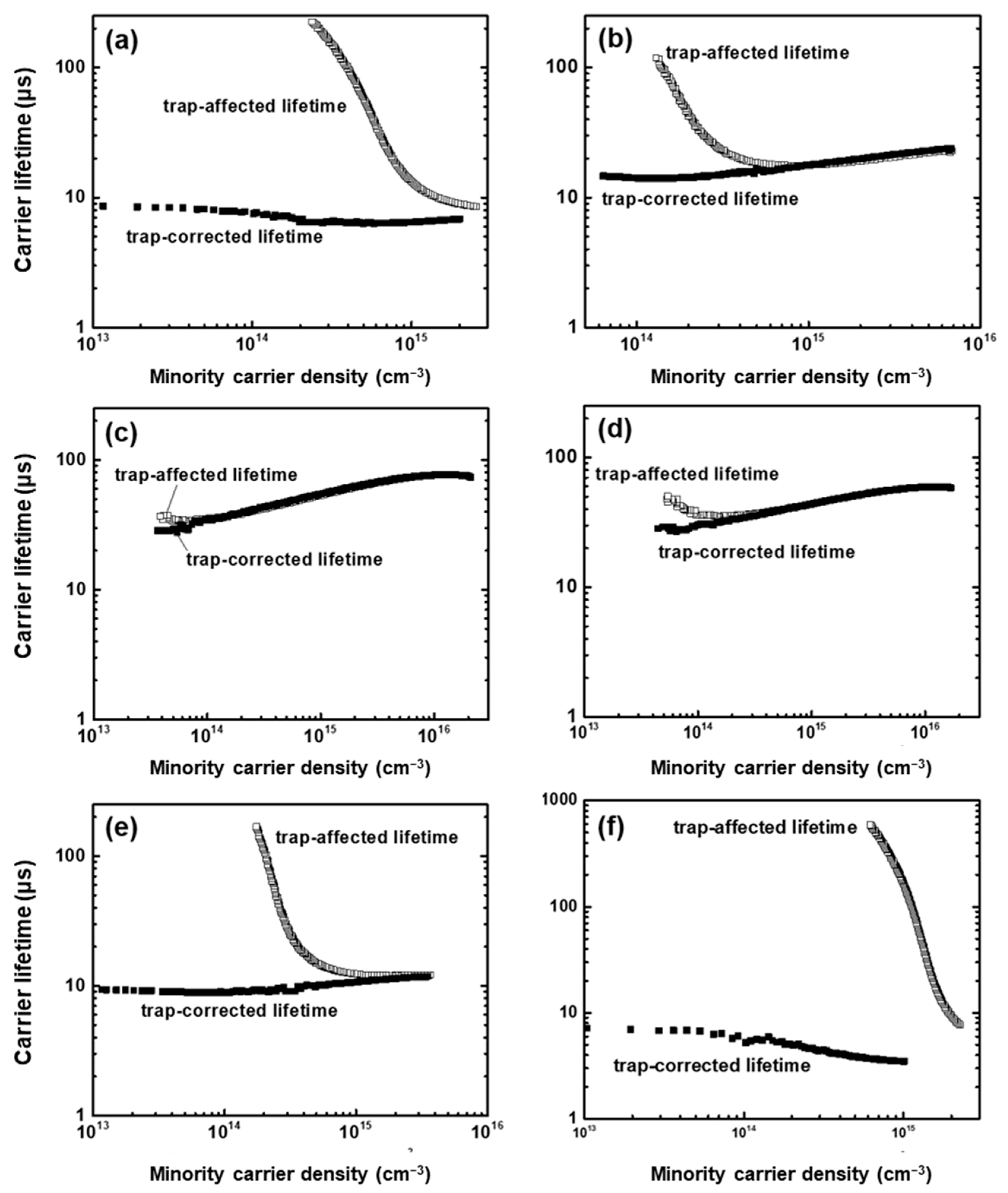
Figure 3 shows the results of the extraction of the corrected carrier lifetime from the measurement results (trap-affected lifetime). Samples are defined as (a) 0 °C (initial), (b) 450 °C, (c) 550 °C, (d) 650 °C, (e) 750 °C and (f) 850 °C. As the annealing temperature increases from 0 to 450 °C, the gap between the trap-affected and trap-corrected lifetimes decreases and then increases again at 650 °C.
Figure 3c exhibits a minimized trapping effect, confirming a carrier lifetime of ~54 μs at 1.0 suns. In contrast, sample F with a maximized trapping effect exhibited a carrier lifetime of ~10 μs at 1.0 suns. The density of the trap center (Ntrap) was extracted using the trap-corrected excess carrier density by bias-light intensity (
) using
where
fabs is the fraction of incident photons absorbed, presented as a function of the particular optical properties of the sample,
τmeasured is the measured carrier lifetime,
q is fundamental charge, and
W is the wafer thickness. The detailed theoretical formulas and methods of the analysis have been described by Macdonald et al. [
22].
Figure 4 shows the results of the analysis of the
Ntrap density as a function of annealing temperature. The
Ntrap density has a relatively large value of 5.2 × 10
14 cm
−3 for sample A and 2.2 × 10
12 cm
−3 for sample C (550 °C), indicating a significant decrease in the number of
Ntrap. Meanwhile, sample F (850 °C) has a fairly large
Ntrap density of 1.2 × 10
15 cm
−3. The results indicated that the increase or decrease in the trapping effect is attributed to the change in the trap-center density in mc-Si.
To determine whether this change was caused by the behavior of the hydrogen in the SiN
x:H thin film, the variation in the amount of hydrogen and its distribution were investigated using ToF-SIMS.
Figure 5 shows the results of the measured amount of hydrogen in the samples according to the changes in the annealing temperature.
At the annealing temperatures of 450 and 550 °C, a similar amount of hydrogen is noted, as shown in
Figure 5a. This decreases at 650 and 850 °C, as shown in
Figure 5b. Hydrogen mapping analysis was also performed in the grain area of the mc-Si wafer to clearly observe the hydrogen distribution. As shown in
Figure 6, hydrogen has a uniform distribution at 0, 450, 550, and 650 °C. However, at 750 and 850 °C, hydrogen is almost entirely released, accumulating in some local areas. The reduction in the carrier lifetime at a high injection level (>10
15 cm
−3) shown in
Figure 2 can be attributed to the deterioration of the passivation properties of the grain area in the mc-Si wafer. The hydrogen distribution of the grain boundary area in the mc-Si wafer is also noted to be related to the trapping effect.
Figure 7 shows the hydrogen distribution in the grain boundary area obtained using an APT measurement. The initial sample (
Figure 7a) showed that the hydrogen distribution did not entirely fill the grain boundary area. In contrast, at an annealing temperature of 550 °C (
Figure 7b), hydrogen sufficiently filled the grain boundary area, whereas at 850 °C (
Figure 7c), the highest hydrogen emission is noted with lesser hydrogen in the grain boundary area than in the initial sample. This is considered as clear evidence of the change in the trapping effect, thereby decreasing and then increasing the carrier lifetime at a low injection level.
To confirm the in-diffusion and out-diffusion energies of hydrogen in the grain boundary area, the activation energy was extracted using an Arrhenius plot based on the change in
Ntrap at different annealing temperatures, as show in
Figure 4. The equation for the Arrhenius plot used to extract the activation energy is
where
Ntrap,0 is the density in the initial state,
EA is the activation energy,
k is the Boltzmann constant, and
T is the absolute temperature. As a shown in
Figure 8, hydrogen has an in-diffusion activation energy of approximately 0.181 eV and out-diffusion activation energy of 1.181 eV. From these results, grain boundary passivation by hydrogen requires a relatively low in-diffusion activation energy, while emission energy from the grain boundary of the passivated hydrogen is 10 times more than the in-diffusion activation energy.
Therefore, the trapping effect decreases at the low temperature region (0–550 °C) due to the improvement of grain boundary passivation properties by the in-diffusion of hydrogen, whereas it increases at the high temperature region (650–850 °C) due to the deterioration of the grain boundary passivation properties by out-diffusion of hydrogen.

 ,
, 


