Abstract
Organic–inorganic perovskites are crystalline light absorbers which are gaining great attraction from the photovoltaic community. Surprisingly, the power conversion efficiencies of these perovskite solar cells have rapidly increased by over 25% in 2019, which is comparable to silicon solar cells. Despite the many advances in efficiency, there are still many areas to be improved to increase the efficiency and stability of commercialization. For commercialization and enhancement of applicability, the development of electron transport layer (ETL) and its interface for low temperature processes and efficient charge transfer are very important. In particular, understanding the ETL and its interface is of utmost importance, and when this understanding has been made enough, excellent research results have been published that can improve the efficiency and stability of the device. Here, we review the progress of perovskite solar cells. Especially we discuss recent important development of perovskite deposition method and its engineering as well as the electron transport layer.
1. Introduction
Perovskite solar cells, since Miyaska et al. reported the organic–inorganic perovskite solar cells [1], have been considered to be a promising candidate as a future energy source because of their potential for very low cost and high efficiency. The perovskite crystalline light absorbers could be easily synthesized by combining an organic and inorganic sources which usually have ABX3 composition [2,3,4]. Resulting perovskites have large absorption coefficient [5], long diffusion length [6], and small exciton binding energy [7]. After solution-processed perovskite material is applied to the solid state solar cell, the efficiency is accelerated, which changed the history of photovoltaics [2,8]. With the rapid growth of efficiency, now over 25% of high-efficiency perovskite solar cell is reported [9], it reached a similar efficiency level to copper indium gallium diselenide (CIGS) solar cells [10], and researches are trying to reach the efficiency of commercial monocrystalline silicon cells.
To achieve the highly efficient perovskite solar cells, not only the materials of ETL (electron transport layer)/perovskite/HTL (hole transport layer), but interface of ETL/Perovskite and Perovskite/HTL should be considered carefully.
According to the material and interface, the device shows different charge generation, electron transport, and blocking recombination behavior in perovskite solar cells. In particular, the electron transfer rate at the ETL/perovskite interface is known to be slower than the hole transfer rate at the perovskite/HTL, which affects not only the hysteresis behavior in efficiency measurement and recombination in device, but also the device stability such as ion migration [11]. Therefore, ETL material selection and engineering are very important to achieve high-efficiency, and highly stable perovskite solar cells.
Up to now, most of the high-efficiency perovskite solar cells are obtained from the structure of n-i-p, and in here, n-type material plays and important role. In high-efficiency n-i-p perovskite solar cell device, mainly meso-porous layer (which requires a high-temperature process) is employed, which is expensive for mass production. For the commercialization of perovskite, an n-type capable of high efficiency and stability of the device is required. In particular, for mass production or flexible device applications, n-type material and engineering are required that can be prepared at low temperatures and provides high efficiency and stability as high as high-temperature processes n-type material. Due to this importance, most of noticeable development in perovskite solar cells were done by engineering perovskite and electron transport layer.
Up to now, TiO2 or SnO2 has been used as an n-type material in high-efficiency devices, and studies have been conducted to increase the efficiency and stability of devices through small changes in materials or interface engineering. In addition, studies on new ETL and interface engineering have shown many possibilities, but do not show the same efficiency and stability as TiO2 or SnO2.
In this review, we will explore the noteworthy achievements in hybrid perovskite solar cells in ETL and its engineering and look at the direction we are going forward.
2. Materials
The ETL plays a key role in the device to extract the electrons from the perovskite layer and block the recombination between electrons in the FTO and holes in the perovskite layer. Up to now, TiO2 has been used as an ETL in most reported PSCs [12]. TiO2 ETLs were widely applied in dye-sensitized solar cells. The conduction band maximum (CBM) and valence band maximum (VBM) of TiO2 are −4.4 eV and −7.63 eV, respectively, which guarantee not only efficient electron transport from the perovskite layer but efficient hole-blocking ability at the perovskite interface [13]. TiO2 film fabrication usually requires a high-temperature process, but recently, colloid-spray coating method was reported enabling 100 °C fabrication of TiO2 layer [14]. We reported that the thickness and contact optimization of the TiO2 ETL is important to get maximized efficiency [15]. However, too thick ETL can minimize the recombination in the device; the electron flow may be hampered due to the high resistance. Thus, contact between FTO and ETL should be considered carefully. TiO2 surface properties can also be controlled and they affect to the device performance. When the bare TiO2 compact layers were treated with TiCl4 and UV ozone, a device treated with TiCl4 showed better surface coverage on the FTO; and a UV treated one showed increased hydrophilicity and increased device performance [16]. In PSCs, two kinds of TiO2 ETL which are compact and meso-porous layer were used [2,12,17,18,19,20,21]. Thin compact layers were deposited on the FTO substrate which were deposited by spin-coating [22], spray pyrolysis [23,24], sol-gel [25], chemical bath deposition [26], and atomic layer deposition (ALD) methods [27]. A TiO2 nano sheet with the perovskite was also employed by eliminating HTM [17]. In meso-porous devices, electrons can be transported through both perovskite and meso-porous layers. Thus, TiO2, which has relatively low mobility (~10−4 cm2 V−1 s−1) [28], was enough to collect the electrons with hysteresis-free behavior. However, without a meso-porous layer, an interface between ETL and perovskite was fully responsible for separating and transporting electrons.
This imbalance of electron and hole mobility cause the hysteric behavior in TiO2 meso-porous skipped devices (in Al2O3 meso-porous and planar devices.) [8,29]. Thus most of the developments in ETLs have been conducted in the planar device to improve not only their efficiency but reduce the hysteresis. This hysteresis behavior caused the different device efficiency according to the measuring environment such as scan direction and scan speed [29,30,31,32,33,34,35,36]. Such phenomena came from trapping electronic carriers, ion migration, and ferroelectric effect of perovskite (Figure 1a) [34,36]. To control these factors, appropriate ETL should be selected. Even ETL free perovskite solar cell with relatively high 13.5% of efficiency was reported [37], which was obtained only from fast current density-voltage (J-V) scan. Generally, maximum power point (MPP) measurement is accepted as a reliable result to evaluate the device efficiency [29] and the MPP efficiency of no ETL device reported as ~0%. A fast scan device could get a relatively high efficiency due to the ion migration at the interface since the pre-bias applied before measuring the device (Figure 1b). However, after it stabilized, the ion would be redistributed and the device cannot get this advantage anymore (Figure 1c) [38]. The permanent built-in potential in the device is very important to maintain the device efficiency for a long time. We also reported that in an ETL free planar device, the ethoxylated polyethylenimine (PEIE) generated the induced dipole in the device which provided a permanent built-in potential for the device result in 12.7% of MPP efficiency [28]. Thus, interfacial engineering at ETL/perovskite is the most vital factor to increase the device performance. An ideal interface has small series resistance (Rs) with large shunt resistance (Rsh) and recombination resistance (Rrec). These resistance values critically affect to the short circuit current density (JSC) of the device; thus to reduce the resistance of electron transport, ETL should have well matched energy level to facilitate electron injection and hole blocking. In addition, electron mobility of the material should be high enough [39]. Therefore, design of the appropriate ETL is really crucial to improve the device efficiency. We summarized the energy level of the ETL materials which have been introduced with high mobility in Figure 2.
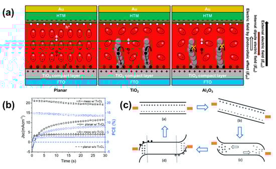
Figure 1.
(a) Schematic illustration of planar, meso-porous TiO2, and Al2O3 scaffolds perovskite device under applied electric field, and plausible physical mechanism of the polarization in ferroelectric perovskite. Reprint with permission [34]; 2015, American Chemical Society. (b) Stabilized maximum power point (MPP) measurement with and without compact layer (c) Schematic illustration of the ion migration at pre-biased state. Reprint with permission [38]; 2015, Royal Society of Chemistry.
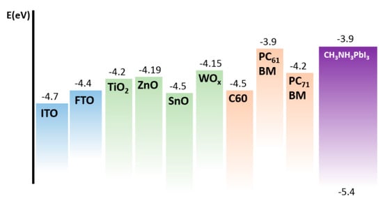
Figure 2.
Summary of energy level of electron transport layer (ETL) materials and perovskite.
ZnO is one of the promising materials as an ETL with −4.19 eV of CBM [11,36]. It has a direct band gap of 3.3 eV and compared the TiO2, the ZnO has conductivity several orders of magnitude higher [40,41] than that of TiO2. Thus, the ZnO could reduce the recombination loss in the device significantly. In addition, ZnO does not need the high temperature sintering process which is ideal for deposition on thermally sensitive substrates (flexible substrate) [42,43].
The low temperature ZnO was employed by cathodic electron deposition to apply the flexible perovskite (Figure 3a) [44]. Of the compact ZnO layer, 50–200 nm was deposited on the flexible substrate which has angular grains (Figure 3b,c). The resulting flexible device showed 8.9% of efficiency. Sol-gel type of ZnO was also introduced due to its simple fabrication process at room temperature processed perovskite solar cells (Figure 3d) [45]. The resulting perovskite solar cell showed 15.7% and 10.2% efficiency of the conventional and flexible device which maintained its efficiency after bending test (Figure 3e,f).
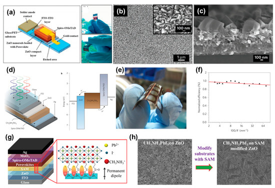
Figure 3.
(a) Schematic illustration of the architecture for the perovskite devices. (b) Top down and (c) cross-sectional SEM images of the ZnO compact layer electrodeposited on FTO. Reprint with permission [44]; 2013, Royal Society of Chemistry. (d) Device structure and energy diagram of ITO/ZnO/CH3NH3PbI3/spiro-OMeTAD/Ag cells. (e) Photo of flexible device, (f) normalized PCE (measured on a flat device) after first bending the substrate. Reprint with permission [45]; 2014, Springer Nature. (g) Schematic illustration of perovskite solar cell employing self- assembled monolayer (SAM) device. (h) Top down images of perovskite on the FTO and modified ZnO. Reprint with permission [46]; 2015, American Chemical Society.
This low efficiency could be improved by forming a dense and compact perovskite layer. To control the morphology of the perovskite on the ZnO compact layer, self-assembled monolayer (SAM) was employed on the ZnO compact layer (Figure 3g). ZnO-SAM compact layer changed the surface properties of the substrates, improving the crystallization and morphology of perovskite layer (Figure 3h) resulting in increased efficiency as high as 15.7% [46]. However, ZnO has a degradation problem like TiO2 does, which will reduce the device stability [47,48].
Therefore, researchers have tried to find other new ETL material. Recently, SnO2 has been attracting much attention as a promising ETL in p-PSCs. The SnO2 particles prepared by low temperature process showed better electronic property than that of prepared by high temperature process. Low temperature processed SnO2 introduced to the sequentially deposited perovskite and vacuum processed perovskite which showed 13% and 15.1% of efficiency respectively [49,50]. Due to the low temperature process (<150 °C), excellent optical and electrical properties (~10−3 cm−1 v−1 s−1) [51] of SnO2, it is employed in many p-PSC [52]. After several rounds of optimizing, the efficiency was increased over 23% [53,54]; however, there was hysteresis between forward and reverse scan efficiency [55]. To overcome this hysteric problem, (FAPbI3)0.85(MAPbBr3)0.15 mixed perovskite was combined with the SnO2 to make a barrier free electron transporting interface. Lower CBM of SnO2 provided the barrier free band alignment between the perovskite and the charge selective contact which removed the hysteresis in the device with high efficiency of 18.4% (Figure 4a,b) [56]. In addition, ALD and chemical bath deposition (CBD) were employed (Figure 4c) to achieve the better contact with the FTO substrate and perovskite on the FTO (Figure 4d) resulted in high efficiency of 19 and 20.8% (Figure 4e), respectively, with high electron extract efficiency (Figure 4c–e) [57]. Apart from the ZnO and SnO2, other inorganic materials are also employed as an ETL [58]. Low temperature process Cs2CO3 was employed on the ITO with 14.4% of high efficiency but it was troublesome in the process because it needed to be repeated to get a desired layer thickness [59]. Indium tin oxide (ITO) was also introduced on the FTO substrate but the device showed high efficiency of 13% only when it was combined with the phenyl-C61-butyric acid methyl ester (PCBM) layer [60]. Low temperature solution processed amorphous WOx was also employed [61,62]. ZnSnO4 was employed to the flexible device by reacting ZnCl2 with SnCl4 which showed high efficiency of 14.4% but it showed hysteresis at the forward scan [63]. In addition, hybrid TiO2/ZnO, was also introduced [64].
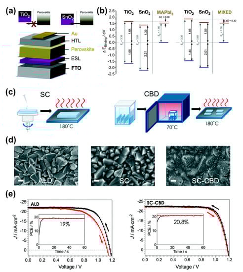
Figure 4.
(a) Energy band diagram of the perovskite films and the ETL in the planar device with schematic energy band and electron flow in the device. (b) Energy band of TiO2 and SnO2 with MAPbI3 and (FAPbI3)0.85(MAPbBr3)0.15. Reprint with permission [56]; 2015, Royal Society of Chemistry. (c) Schematic illustration of preparation of SnO2 by spin coating and chemical bath deposition. (d) Top view images of SnO2 prepared by ALD, SC and SC-CBD methods. (e) J-V and MPP efficiency of the device employed SnO2 and transient absorption measurement of SnO2 and TiO2 based p-PSC. Reprint with permission [57]; 2015, Royal Society of Chemistry.
Organic electron transport layer also employed instead of inorganic ETL. Fullerene derivatives are used mainly as ETL. PCBM is one of the most common fullerene derivative which is modified of C60 fullerene. Even C60 has higher mobility (6.1 cm2 V−1 s−1) and conductivity (2.3 × 10⁻³ Scm−1) than the PCBM (1.6 cm2 V−1 s−1 and 3.2 × 10⁻³ Scm−1, respectively); it is not commonly employed due to its poor solubility in common organic solvent [65]. These fullerene and fullerene derivatives are usually demonstrated in p-i-n structured device due to the low solvent resistance of C60 and PCBM. It is well known that the C60 and its derivative could be washed by organic solvent such as DMF and CB which are common solvents used in perovskite precursor and Spiro-MeOTAD solution [65]. Partially-washed sites could create a shunting pathway and lead hysteresis. Thus, it showed lower efficiency than the conventional n-i-p type device because of low hole mobility and acidic nature of PEDOT: PSS [66]. Recently, modified fullerene derivatives were introduced by cross-linking the fullerenes’ derivatives with each other. The resulting ETL showed increased solvent resistance to the DMF and C60, which also requires a synthesis process [67].
Another approach to improve carrier transport in perovskite solar cells is dipole formation between electrode and perovskite by ionic species. Asymmetry functional group on the metal oxide such as FTO or SnO2 produce the dipole moment leading to fast electron extraction [28]. Since ionic liquid is considered as the suitable material for devices [68], there are several attempts to induce the ionic liquids to perovskite solar cells. In 2018, 1-benzyl-3-methylimidazolium chloride-treated SnO2 based perovskite solar cell was reported [69]. The binding between Sn and electronegative anion of ionic liquid generated perovskite-faced interfacial dipole, leading to reduced RS and improved JSC.
3. Structure and Engineering
To overcome the shortage of nanoparticles, metal oxide nanostructures are fabricated and applied in various research fields such as energy, materials, optics, photonics, and many other physics and electrochemistry areas such as battery, catalysis, fuel cell, sensor, solar cell, and transistor [70]. Basically, nanostructures have an advantage of large surface area and tuned band gap which could give benefit in electrochemistry fields [71]. In addition, the nano-scale size and unusual shape of the nanostructure have shown unique properties [72]. Thus, many researchers have employed these nanostructures as an ETL in perovskite solar cell as well.
Among them, due to their well-matched energy level and electrical properties, many TiO2 nanostructures have been developed for applying solar cells. Common TiO2 nanostructures have a large active area and could enhance the photoelectric properties compared to bulk TiO2 structure. Therefore, ETL which is consisted of TiO2 nanostructures, could provide the improved electron collection and transport with preventing recombination in the dye sensitized solar cells [73,74]. Following the rapid development of perovskite solar cells, many TiO2 nanostructures are applied to improve the device performance [75,76,77,78,79] which successfully increases the power conversion efficiency by enhancing the electron mobility and charge separation at the ETL/perovskite interface compared to the conventional perovskite solar cells [78,80]. Longer length and thinner film thickness of nanostructures such as nanorod, nanofiber, and rutile could provide fast electron diffusion coefficient and lower recombination rate resulting in improved efficiency of 9.4% and 9.82%, respectively [75,76]. Moreover, 1-D nanostructures, such as nanorod and nanotube, could provide a direct electron transport pathway which could be optimized in the synthesis condition. For instance, ZnO-TiO2 core-shell nanostructure (TiO2 covered ZnO nanorod) provides more improved film morphology without UV ozone treatment or TiCl4 surface treatment and enhanced band gap. Thus 1-D ZnO-TiO2 core-shell nanorod which was grown in charge transport direction demonstrate 15.3% of PCE with increased open-circuit voltage (VOC) and short-circuit current (JSC) [79]. In the same way, nanostructured ETL, which consist of TiO2 on the SnO2 nanowire, also showed improved efficiency of 14.2% [81].
Perovskite crystal growing on nanostructure is another major issue. Grain size and film morphology of perovskite crystal is very sensitive according to the property of substrate, so perovskite crystal on the nanostructure exhibits various properties. This phenomenon even interrupts the optimization of devices but can bring the advantage of meso-structured perovskite solar cells, which is the formation of perovskite bilayer due to the difference between the inside and outside of the nanostructure [82]. Combination of small size crystal layer at the nanostructure and large size crystal layer on the small size one carries out the enhanced charge collection and light absorption [4,83].
Moreover, TiO2 morphology control and crystal phase control in nano-scale can be good a trial for highly efficient perovskite solar cells. Due to the large roughness of FTO glass ETL layer on the FTO glass have irregular film thickness with many defects. However, using an anodization method for single crystalline, uniform thickness, and defect-free TiO2 nanostructure which provides efficient electron extraction and hole blocking was demonstrated. Thus, planar perovskite solar cell devices using anodized TiO2 ETL has high efficiency and solves the usual problem of planar device structure such as high hysteresis and small surface contact area at ETL/perovskite interface [15]. Figure 5 shows the anodizing method, transmission electron microscope (TEM) image, and its electron energy loss spectroscopy (EELS) image of anodized TiO2 ETL. Resulting nanostructure showed regular thickness with excellent transparency result in 13.5% of efficiency.
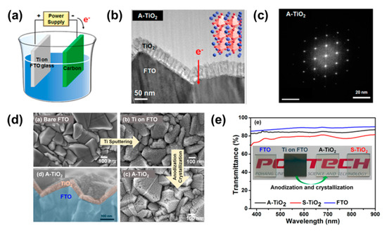
Figure 5.
(a) Illustration of anodizing process. (b) Cross-sectional TEM image of anodized TiO2 (c) electron energy loss spectroscopy (EELS) image of resulting nanostructure. (d) Top down and cross-sectional SEM images of nanostructure on FTO substrate. (e) Transparent measurement of anodized and spin-coated TiO2 layer on FTO substrate. Reprint with permission [15]; 2016, American Chemical Society.
Instead of TiO2 which is hard to applied low temperature process, other band gap suitable oxide nanostructure materials such as ZnO was also employed in perovskite solar cells [45]. By controlling the concentration of ZnO precursor solution and immersion time, various diameters and lengths of nanorods were fabricated. Well optimized ZnO nanorod ETL gave 11.1% of efficiency which showed efficient charge collection than TiO2 nanorod [84].
In addition, an anodizing method can provide the defect-free multi-layered ETL for photovoltaic devices, serving a deep understanding of carrier extraction. The carrier extraction is dominated by mobility of the transport layer and the gap of Gibbs free energy between the transporting layer and perovskite in solar cells. The case study on single SnO2, TiO2, SnO2@TiO2, and TiO2@SnO2 application on perovskite proved that the large free energy difference between perovskite and contact material was effective to extract the electron when the mobility of ETL was higher than 10−4 cm2 V−1 s−1 [85]. Figure 6a shows the scheme and efficiency of the modified ETLs-based perovskite solar cells. By separating a contact material and a transport material, the relationship between electron extraction and Gibbs free energy/mobility was successfully investigated. Using anodized high-crystalline defect-free TiO2 deposition and spin-coated SnO2 with deep energy level, the perovskite solar cell achieved 21.1% in 2017 (Figure 6b). More recently, Wang et al. reported In2O3/SnO2 bi-layered ETL-based perovskite solar cell showing minimized VOC loss and high device stability. These enhancements were originated from the gradient energy alignment of ETL [86]. The gradient energy alignment of the transport layer was typical of the structure design for efficient perovskite solar cell today [87].
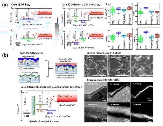
Figure 6.
(a) Illustration and J-V characteristics of different Gibbs free energy and electron mobilities; SnO2, TiO2, SnO2@TiO2, and TiO2@SnO2. (b) Illustration and SEM image of SnO2 on anodized TiO2 layer. Reprint with permission [85]; 2017, American Chemical Society.
One of the problems with p-PSC in low temperature processes is its stability. In many p-PSCs, it has been pointed out that the operation stability is relatively lower than that of the TiO2 meso-based device to which the high temperature process is applied [88]. This is due to imbalance resulting from the difference between the moving speeds of the electrons and holes, thus the electrons cannot be efficiently collected to the electrode at the ETL/perovskite interface, resulting in recombination taking place. This is due to the imbalance resulting from the difference between the hole movement speed and the electron movement speed, and recombination occurs without efficiently transferring charges at the ETL/perovskite interface [89,90]. To solve this problem, studies on improving electrical properties through engineering of ETL/Perovskite interfaces are actively being conducted.
For example, zwitterion-treated SnO2 was introduced to perovskite solar cells, showing 21.4% PCE with enhanced thermal stability in 2018 [91]. This zwitterion materials could make dipole moment at the interfaces, leading to inducing driving force of electrons. More recently, tuned work function of SnO2 and trap passivation of perovskite produced by zwitterion served the higher PCE and longer device stability compared to the reference device [92,93]. In addition, many studies are being conducted to improve the efficiency and stability of devices through interfacial modification using organic molecules on SnO2 [94,95]. Furthermore, biological polymer treatment on SnO2 ETL could control the crystal align of perovskite, improving interface contact and device stability of solar cells [96].
Recently, ETL/perovskite engineering has been reported that performs a dual function of passivating perovskite traps while at the same time changing the surface properties using creatine self-assembly properties for SnO2 [97]. In addition to the organic molecule, an inorganic chemical was also added to improve the quality of the low-temperature processed SnO2 layer. Zhu et al., employed the SnO2-KCl composite ETL to simultaneously passivate the defects at the ETL/perovskite interface and the grain boundaries of perovskite film [98].
Furthermore, this surface treatment strategy can be conducted to flexible devices to improve efficiency of perovskite solar cells. For example, a fullerene has superior electrical properties to replace solid metal oxide layer in optoelectronic device, but also has critical adhesion problem. Song et al. reported that the mixture of fullerene and poly(allylamine) provided enhanced solvent resistance and adequate energy level, achieving 15.1% efficiency of flexible perovskite solar cell (Figure 7a) [99]. The improved characteristics of the interface were investigated by contact angle and electron dynamic measurement systems such as space charge limited current, time-resolved photoluminescence, and impedance analysis (Figure 7b).
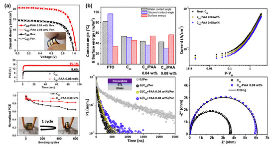
Figure 7.
(a) J-V curve, device stability, and bending test of flexible perovskite solar cell using fullerene and poly(allylamine) (C60-PAA). (b) Contact angle, space charge limited current, time-resolved photoluminescence, and impedance analysis of FTO/C60-PAA based devices. Reprint with permission [99]; 2018, Elsevier.
Doping is other good way to improve the properties of ETL. By doping the material, electron mobility or energy level of the ETL could be enhanced which affects the device performance. An Mg-doped TiO2 layer increased the energy level of ETL which could give the increased VOC value in the perovskite device. Moreover, magnesium oxide and magnesium hydroxide, which formed at ETL/perovskite interface, hinder the recombination in the device result and improved VOC was obtained, thus the resulting perovskite solar cell showed 12.3% of efficiency mainly due to the increased VOC [100]. Zr-doped TiO2 also formed a ZrxTi1−xO2 which moved the energy level of TiO2 resulting in improved VOC with 9.8% efficiency [101]. The device efficiency was also improved by doping of Al. When the Al-doped on TiO2 ETL, traps in the TiO2 were filled by Al, thus, the traps were passivated resulting in a decrease of defect sites. The resulting ETL efficiently blocked the electron recombination which gave 13.8% of efficiency (Figure 8) [102]. Sn was also employed as a doping material on TiO2 ETL. Unlike other doping materials, JSC was increased due to the increased electron mobility with decreased transport resistance [103].
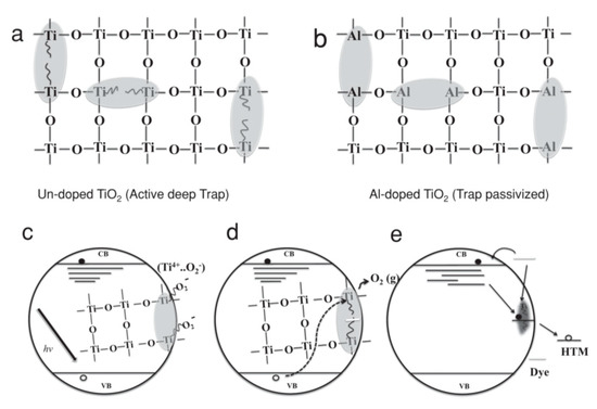
Figure 8.
Al doped TiO2 and the passivation of traps by Al. (a) Oxygen defect inducing deep electronic traps in TiO2. (b) Al substitution passivating oxygen traps. (c) Trap passivation produced by ionization of Ti. (d) Neutralized Ti by holes, which (e) enables charge recombination. Reprint with permission [102]; 2014, STM Signatory.
4. Conclusions and Outlook
Recently, rapid and impressive developments have been achieved in perovskite solar cell field. Understanding of the perovskite materials and electron transport layers (ETL) heavily contribute to this achievement. In this review article, we have given an overview of a historical development of perovskite solar cells focused on the perovskites and electron transport materials. Morphology control, perovskite engineering, and ETL material selection were described to be important factors which directly affect the device performance. Moreover, the correlation between device structures and its required ETL and perovskite characters were also discussed, which is also of great importance to achieve the efficient planar perovskite solar cells. Fabrication methods, including one, two step, vacuum processes, and solvent engineering were shown to influence the crystal growth and the morphology of perovskite. In addition, by choosing the effective ETL, charges from the perovskite effectively separated, thereby impacting on the power conversion efficiency of solar cells. This result indicates that the importance of material and morphology control of perovskite solar cells. So far, the champion cells have been based on the meso-device. However, after engineered the material and interface, perovskite solar cell could show highly efficient performance with simplified structure with flexible application.
The development of perovskite solar cells mainly relies on the composition of perovskite. The composition change of perovskite can improve not only increasing device characteristics of perovskite solar cells but also leading the way to the future-oriented solar cells such as flexible, transparent, or Pb-free perovskite. As perovskite material evolves, it is too self-evident that the deep study of suitable ETLs should be accompanied. For example, it seems that the conventional metal oxide layer with Pb-free Sn-based perovskite cannot fabricate efficient solar cells. Besides, in the near future, new perovskite may require aligned lattice and crystal face orientation to achieve high-crystalline and high-stable perovskite crystal. These needs cannot be satisfied by current metal oxides and will be achieved by continuing the exploration of new materials and deep understanding of electron transfer in the devices.
Author Contributions
Conceptualization, S.S. and J.L.; investigation, S.S and T.K.; resources, S.S. and T.K.; writing—original draft preparation, S.S.; writing—review and editing, J.L. and T.K. All authors have read and agreed to the published version of the manuscript.
Funding
This Research has been performed as a project No KS2022-10 (Advanced materials for low-cost and high-performance solar cells) and supported by the KOREA RESEARCH INSTITUTE of CHEMICAL TECHNOLOGY(KRICT). J.L. acknowledges the supports by research fund of Chungnam National University and also by the National Research Foundation of Korea(NRF) grant funded by the Korea government(MSIT) (No. 2020R1G1A1102777).
Conflicts of Interest
The authors declare no conflict of interest.
References
- Kojima, A.; Teshima, K.; Shirai, Y.; Miyasaka, T. Organometal halide perovskites as visible-light sensitizers for photovoltaic cells. J. Am. Chem. Soc. 2009, 131, 6050–6051. [Google Scholar] [CrossRef] [PubMed]
- Kim, H.S.; Lee, C.R.; Im, J.H.; Lee, K.B.; Moehl, T.; Marchioro, A.; Moon, S.J.; Humphry-Baker, R.; Yum, J.H.; Moser, J.E.; et al. Lead iodide perovskite sensitized all-solid-state submicron thin film mesoscopic solar cell with efficiency exceeding 9%. Sci. Rep. 2012, 2, 591. [Google Scholar] [CrossRef] [PubMed]
- Liu, M.; Johnston, M.B.; Snaith, H.J. Efficient planar heterojunction perovskite solar cells by vapour deposition. Nature 2013, 501, 395–398. [Google Scholar] [CrossRef]
- Burschka, J.; Pellet, N.; Moon, S.J.; Humphry-Baker, R.; Gao, P.; Nazeeruddin, M.K.; Gratzel, M. Sequential deposition as a route to high-performance perovskite-sensitized solar cells. Nature 2013, 499, 316. [Google Scholar] [CrossRef] [PubMed]
- Park, N.G. Organometal Perovskite Light Absorbers toward a 20% Efficiency Low-Cost Solid-State Mesoscopic Solar Cell. J. Phys. Chem. Lett. 2013, 4, 2423–2429. [Google Scholar] [CrossRef]
- Stranks, S.D.; Eperon, G.E.; Grancini, G.; Menelaou, C.; Alcocer, M.J.; Leijtens, T.; Herz, L.M.; Petrozza, A.; Snaith, H.J. Electron-hole diffusion lengths exceeding 1 micrometer in an organometal trihalide perovskite absorber. Science 2013, 342, 341–344. [Google Scholar] [CrossRef] [PubMed]
- Miyata, A.; Mitioglu, A.; Plochocka, P.; Portugall, O.; Wang, J.T.W.; Stranks, S.D.; Snaith, H.J.; Nicholas, R.J. Direct measurement of the exciton binding energy and effective masses for charge carriers in organic-inorganic tri-halide perovskites. Nat. Phys. 2015, 11, 582–594. [Google Scholar] [CrossRef]
- Lee, M.M.; Teuscher, J.; Miyasaka, T.; Murakami, T.N.; Snaith, H.J. Efficient hybrid solar cells based on meso-superstructured organometal halide perovskites. Science 2012, 338, 643–647. [Google Scholar] [CrossRef]
- Jung, E.H.; Jeon, N.J.; Park, E.Y.; Moon, C.S.; Shin, T.J.; Yang, T.-Y.; Noh, J.H.; Seo, J. Efficient, stable and scalable perovskite solar cells using poly (3-hexylthiophene). Nature 2019, 567, 511–515. [Google Scholar] [CrossRef]
- Repins, I.; Contreras, M.A.; Egaas, B.; DeHart, C.; Scharf, J.; Perkins, C.L.; To, B.; Noufi, R. 19.9%-efficient ZnO/CdS/CuInGaSe2 solar cell with 81.2% fill factor. Prog. Photovolt. 2008, 16, 235–239. [Google Scholar] [CrossRef]
- Calado, P.; Telford, A.M.; Bryant, D.; Li, X.; Nelson, J.; O’Regan, B.C.; Barnes, P.R. Evidence for ion migration in hybrid perovskite solar cells with minimal hysteresis. Nat. Commun. 2016, 7, 1–10. [Google Scholar] [CrossRef] [PubMed]
- Im, J.H.; Lee, C.R.; Lee, J.W.; Park, S.W.; Park, N.G. 6.5% efficient perovskite quantum-dot-sensitized solar cell. Nanoscale 2011, 3, 4088–4093. [Google Scholar] [CrossRef] [PubMed]
- Seo, Y.S.; Lee, C.; Lee, K.H.; Yoon, K.B. 1:1 and 2:1 charge-transfer complexes between aromatic hydrocarbons and dry titanium dioxide. Angew. Chem. Int. Ed. 2005, 44, 910–913. [Google Scholar] [CrossRef] [PubMed]
- Paik, M.J.; Lee, Y.; Yun, H.S.; Lee, S.U.; Hong, S.T.; Seok, S.I. TiO2 Colloid-Spray Coated Electron-Transporting Layers for Efficient Perovskite Solar Cells. Adv. Energy Mater. 2020, 2001799. [Google Scholar] [CrossRef]
- Choi, J.; Song, S.; Horantner, M.T.; Snaith, H.J.; Park, T. Well-Defined Nanostructured, Single-Crystalline TiO2 Electron Transport Layer for Efficient Planar Perovskite Solar Cells. ACS Nano 2016, 10, 6029–6036. [Google Scholar] [CrossRef]
- Cojocaru, L.; Uchida, S.; Sanehira, Y.; Nakazaki, J.; Kubo, T.; Segawa, H. Surface Treatment of the Compact TiO2 Layer for Efficient Planar Heterojunction Perovskite Solar Cells. Chem. Lett. 2015, 44, 674–676. [Google Scholar] [CrossRef]
- Etgar, L.; Gao, P.; Xue, Z.; Peng, Q.; Chandiran, A.K.; Liu, B.; Nazeeruddin, M.K.; Gratzel, M. Mesoscopic CH3NH3PbI3/TiO2 heterojunction solar cells. J. Am. Chem. Soc. 2012, 134, 17396–17399. [Google Scholar] [CrossRef]
- Aharon, S.; Gamliel, S.; El Cohen, B.; Etgar, L. Depletion region effect of highly efficient hole conductor free CH3NH3PbI3 perovskite solar cells. Phys. Chem. Chem. Phys. 2014, 16, 10512–10518. [Google Scholar] [CrossRef]
- Bi, D.; Yang, L.; Boschloo, G.; Hagfeldt, A.; Johansson, E.M. Effect of Different Hole Transport Materials on Recombination in CH3NH3PbI3 Perovskite-Sensitized Mesoscopic Solar Cells. J. Phys. Chem. Lett. 2013, 4, 1532–1536. [Google Scholar] [CrossRef]
- Di Giacomo, F.; Razza, S.; Matteocci, F.; D’Epifanio, A.; Licoccia, S.; Brown, T.M.; Di Carlo, A. High efficiency CH3NH3PbI(3−x)Clx perovskite solar cells with poly(3-hexylthiophene) hole transport layer. J. Power Sources 2014, 251, 152–156. [Google Scholar] [CrossRef]
- Abrusci, A.; Stranks, S.D.; Docampo, P.; Yip, H.L.; Jen, A.K.; Snaith, H.J. High-performance perovskite-polymer hybrid solar cells via electronic coupling with fullerene monolayers. Nano Lett. 2013, 13, 3124–3128. [Google Scholar] [CrossRef] [PubMed]
- Hayakawa, A.; Yoshikawa, O.; Fujieda, T.; Uehara, K.; Yoshikawaa, S. High performance polythiophene/fullerene bulk-heterojunction solar cell with a TiOx hole blocking layer. Appl. Phys. Lett. 2007, 90, 163517–163900. [Google Scholar] [CrossRef]
- Cameron, P.J.; Peter, L.M. Characterization of titanium dioxide blocking layers in dye-sensitized nanocrystalline solar cells. J. Phys. Chem. B 2003, 107, 14394–14400. [Google Scholar] [CrossRef]
- Ito, S.; Liska, P.; Comte, P.; Charvet, R.; Péchy, P.; Bach, U.; Schmidt-Mende, L.; Zakeeruddin, S.M.; Kay, A.; Nazeeruddin, M.K. Control of dark current in photoelectrochemical (TiO2/I−–I 3−) and dye-sensitized solar cells. Chem. Commun. 2005, 34, 4351–4353. [Google Scholar] [CrossRef]
- Lee, S.; Cho, I.S.; Lee, J.H.; Kim, D.H.; Kim, D.W.; Kim, J.Y.; Shin, H.; Lee, J.K.; Jung, H.S.; Park, N.G.; et al. Two-Step Sol-Gel Method-Based TiO2 Nanoparticles with Uniform Morphology and Size for Efficient Photo-Energy Conversion Devices. Chem. Mater. 2010, 22, 1958–1965. [Google Scholar] [CrossRef]
- Yella, A.; Heiniger, L.P.; Gao, P.; Nazeeruddin, M.K.; Gratzel, M. Nanocrystalline rutile electron extraction layer enables low-temperature solution processed perovskite photovoltaics with 13.7% efficiency. Nano Lett. 2014, 14, 2591–2596. [Google Scholar] [CrossRef]
- Kim, D.H.; Woodroof, M.; Lee, K.; Parsons, G.N. Atomic Layer Deposition of High Performance Ultrathin TiO2 Blocking Layers for Dye-Sensitized Solar Cells. Chemsuschem 2013, 6, 1014–1020. [Google Scholar] [CrossRef]
- Song, S.; Moon, B.J.; Horantner, M.T.; Lim, J.; Kang, G.; Park, M.; Kim, J.Y.; Snaith, H.J.; Park, T. Interfacial electron accumulation for efficient homo-junction perovskite solar cells. Nano Energy 2016, 28, 269–276. [Google Scholar] [CrossRef]
- Snaith, H.J.; Abate, A.; Ball, J.M.; Eperon, G.E.; Leijtens, T.; Noel, N.K.; Stranks, S.D.; Wang, J.T.; Wojciechowski, K.; Zhang, W. Anomalous Hysteresis in Perovskite Solar Cells. J. Phys. Chem. Lett. 2014, 5, 1511–1515. [Google Scholar] [CrossRef]
- Shao, Y.; Xiao, Z.; Bi, C.; Yuan, Y.; Huang, J. Origin and elimination of photocurrent hysteresis by fullerene passivation in CH3NH3PbI3 planar heterojunction solar cells. Nat. Commun. 2014, 5, 5784. [Google Scholar] [CrossRef]
- Tress, W.; Marinova, N.; Moehl, T.; Zakeeruddin, S.; Nazeeruddin, M.K.; Grätzel, M. Understanding the rate-dependent J–V hysteresis, slow time component, and aging in CH 3 NH 3 PbI 3 perovskite solar cells: The role of a compensated electric field. Energy Environ. Sci. 2015, 8, 995–1004. [Google Scholar] [CrossRef]
- Kim, H.S.; Park, N.G. Parameters Affecting I-V Hysteresis of CH3NH3PbI3 Perovskite Solar Cells: Effects of Perovskite Crystal Size and Mesoporous TiO2 Layer. J. Phys. Chem. Lett. 2014, 5, 2927–2934. [Google Scholar] [CrossRef] [PubMed]
- Unger, E.; Hoke, E.; Bailie, C.; Nguyen, W.; Bowring, A.; Heumüller, T.; Christoforo, M.; McGehee, M. Hysteresis and transient behavior in current–voltage measurements of hybrid-perovskite absorber solar cells. Energy Environ. Sci. 2014, 7, 3690–3698. [Google Scholar] [CrossRef]
- Chen, H.W.; Sakai, N.; Ikegami, M.; Miyasaka, T. Emergence of Hysteresis and Transient Ferroelectric Response in Organo-Lead Halide Perovskite Solar Cells. J. Phys. Chem. Lett. 2015, 6, 164–169. [Google Scholar] [CrossRef] [PubMed]
- Richardson, G.; O’Kane, S.E.; Niemann, R.G.; Peltola, T.A.; Foster, J.M.; Cameron, P.J.; Walker, A.B. Can slow-moving ions explain hysteresis in the current–voltage curves of perovskite solar cells? Energy Environ. Sci. 2016, 9, 1476–1485. [Google Scholar] [CrossRef]
- Beiley, Z.M.; McGehee, M.D. Modeling low cost hybrid tandem photovoltaics with the potential for efficiencies exceeding 20%. Energy Environ. Sci. 2012, 5, 9173. [Google Scholar] [CrossRef]
- Liu, D.; Yang, J.; Kelly, T.L. Compact layer free perovskite solar cells with 13.5% efficiency. J. Am. Chem. Soc. 2014, 136, 17116–17122. [Google Scholar] [CrossRef]
- Zhang, Y.; Liu, M.; Eperon, G.E.; Leijtens, T.C.; McMeekin, D.; Saliba, M.; Zhang, W.; de Bastiani, M.; Petrozza, A.; Herz, L.M. Charge selective contacts, mobile ions and anomalous hysteresis in organic–inorganic perovskite solar cells. Mater. Horiz. 2015, 2, 315–322. [Google Scholar] [CrossRef]
- Liu, H.; Huang, Z.; Wei, S.; Zheng, L.; Xiao, L.; Gong, Q. Nano-structured electron transporting materials for perovskite solar cells. Nanoscale 2016, 8, 6209–6221. [Google Scholar] [CrossRef]
- Fortunato, E.M.; Barquinha, P.M.; Pimentel, A.C.; Gonçalves, A.M.; Marques, A.J.; Martins, R.F.; Pereira, L.M. Wide-bandgap high-mobility ZnO thin-film transistors produced at room temperature. Appl. Phys. Lett. 2004, 85, 2541–2543. [Google Scholar] [CrossRef]
- Nause, J.; Ganesan, S. High-Electron Mobility Transistor with Zinc Oxide. U.S. Patent 7,105,868, 12 September 2006. [Google Scholar]
- Li, F.; Ding, Y.; Gao, P.; Xin, X.; Wang, Z.L. Single-Crystal Hexagonal Disks and Rings of ZnO: Low-Temperature, Large-Scale Synthesis and Growth Mechanism. Angew. Chem. Int. Ed. 2004, 43, 5238–5242. [Google Scholar] [CrossRef] [PubMed]
- Saito, N.; Haneda, H.; Sekiguchi, T.; Ohashi, N.; Sakaguchi, I.; Koumoto, K. Low-temperature fabrication of light-emitting zinc oxide micropatterns using self-assembled monolayers. Adv. Mater. 2002, 14, 418–421. [Google Scholar] [CrossRef]
- Kumar, M.H.; Yantara, N.; Dharani, S.; Graetzel, M.; Mhaisalkar, S.; Boix, P.P.; Mathews, N. Flexible, low-temperature, solution processed ZnO-based perovskite solid state solar cells. Chem. Commun. (Camb.) 2013, 49, 11089–11091. [Google Scholar] [CrossRef] [PubMed]
- Liu, D.; Kelly, T.L. Perovskite solar cells with a planar heterojunction structure prepared using room-temperature solution processing techniques. Nat. Photonics 2014, 8, 133–138. [Google Scholar] [CrossRef]
- Zuo, L.; Gu, Z.; Ye, T.; Fu, W.; Wu, G.; Li, H.; Chen, H. Enhanced photovoltaic performance of CH3NH3PbI3 perovskite solar cells through interfacial engineering using self-assembling monolayer. J. Am. Chem. Soc. 2015, 137, 2674–2679. [Google Scholar] [CrossRef]
- De Jongh, P.; Meulenkamp, E.; Vanmaekelbergh, D.; Kelly, J. Charge carrier dynamics in illuminated, particulate ZnO electrodes. J. Phys. Chem. B 2000, 104, 7686–7693. [Google Scholar] [CrossRef]
- Zhang, H.; Zong, R.; Zhu, Y. Photocorrosion inhibition and photoactivity enhancement for zinc oxide via hybridization with monolayer polyaniline. J. Phys. Chem. C 2009, 113, 4605–4611. [Google Scholar] [CrossRef]
- Song, J.; Zheng, E.; Bian, J.; Wang, X.-F.; Tian, W.; Sanehira, Y.; Miyasaka, T. Low-temperature SnO2-based electron selective contact for efficient and stable perovskite solar cells. J. Mater. Chem. A 2015, 3, 10837–10844. [Google Scholar] [CrossRef]
- Ke, W.; Zhao, D.; Cimaroli, A.J.; Grice, C.R.; Qin, P.; Liu, Q.; Xiong, L.; Yan, Y.; Fang, G. Effects of annealing temperature of tin oxide electron selective layers on the performance of perovskite solar cells. J. Mater. Chem. A 2015, 3, 24163–24168. [Google Scholar] [CrossRef]
- Tiwana, P.; Docampo, P.; Johnston, M.B.; Snaith, H.J.; Herz, L.M. Electron mobility and injection dynamics in mesoporous ZnO, SnO2, and TiO2 films used in dye-sensitized solar cells. ACS Nano 2011, 5, 5158–5166. [Google Scholar] [CrossRef]
- Turren-Cruz, S.-H.; Hagfeldt, A.; Saliba, M. Methylammonium-free, high-performance, and stable perovskite solar cells on a planar architecture. Science 2018, 362, 449–453. [Google Scholar] [CrossRef]
- Jiang, Q.; Zhao, Y.; Zhang, X.; Yang, X.; Chen, Y.; Chu, Z.; Ye, Q.; Li, X.; Yin, Z.; You, J. Surface passivation of perovskite film for efficient solar cells. Nat. Photonics 2019, 13, 460–466. [Google Scholar] [CrossRef]
- Yoo, J.J.; Wieghold, S.; Sponseller, M.C.; Chua, M.R.; Bertram, S.N.; Hartono, N.T.P.; Tresback, J.S.; Hansen, E.C.; Correa-Baena, J.-P.; Bulović, V. An interface stabilized perovskite solar cell with high stabilized efficiency and low voltage loss. Energy Environ. Sci. 2019, 12, 2192–2199. [Google Scholar] [CrossRef]
- Ke, W.; Fang, G.; Liu, Q.; Xiong, L.; Qin, P.; Tao, H.; Wang, J.; Lei, H.; Li, B.; Wan, J.; et al. Low-temperature solution-processed tin oxide as an alternative electron transporting layer for efficient perovskite solar cells. J. Am. Chem. Soc. 2015, 137, 6730–6733. [Google Scholar] [CrossRef]
- Baena, J.P.C.; Steier, L.; Tress, W.; Saliba, M.; Neutzner, S.; Matsui, T.; Giordano, F.; Jacobsson, T.J.; Kandada, A.R.S.; Zakeeruddin, S.M. Highly efficient planar perovskite solar cells through band alignment engineering. Energy Environ. Sci. 2015, 8, 2928–2934. [Google Scholar] [CrossRef]
- Yeo, J.-S.; Kang, R.; Lee, S.; Jeon, Y.-J.; Myoung, N.; Lee, C.-L.; Kim, D.-Y.; Yun, J.-M.; Seo, Y.-H.; Kim, S.-S.; et al. Highly efficient and stable planar perovskite solar cells with reduced graphene oxide nanosheets as electrode interlayer. Nano Energy 2015, 12, 96–104. [Google Scholar] [CrossRef]
- Palilis, L.C.; Vasilopoulou, M.; Verykios, A.; Soultati, A.; Polydorou, E.; Argitis, P.; Davazoglou, D.; Mohd Yusoff, A.R.B.; Nazeeruddin, M.K. Inorganic and Hybrid Interfacial Materials for Organic and Perovskite Solar Cells. Adv. Energy Mater. 2020, 10, 2000910. [Google Scholar] [CrossRef]
- Hu, Q.; Wu, J.; Jiang, C.; Liu, T.; Que, X.; Zhu, R.; Gong, Q. Engineering of electron-selective contact for perovskite solar cells with efficiency exceeding 15%. ACS Nano 2014, 8, 10161–10167. [Google Scholar] [CrossRef] [PubMed]
- Qin, M.; Ma, J.; Ke, W.; Qin, P.; Lei, H.; Tao, H.; Zheng, X.; Xiong, L.; Liu, Q.; Chen, Z.; et al. Perovskite Solar Cells Based on Low-Temperature Processed Indium Oxide Electron Selective Layers. ACS Appl. Mater. Interfaces 2016, 8, 8460–8466. [Google Scholar] [CrossRef] [PubMed]
- Hu, Y.; He, L.; Han, X.; Wang, M.; Yin, Y. Magnetically responsive photonic films with high tunability and stability. Nano Res. 2015, 8, 611–620. [Google Scholar] [CrossRef]
- Wang, K.; Shi, Y.; Li, B.; Zhao, L.; Wang, W.; Wang, X.; Bai, X.; Wang, S.; Hao, C.; Ma, T. Amorphous Inorganic Electron-Selective Layers for Efficient Perovskite Solar Cells: Feasible Strategy Towards Room-Temperature Fabrication. Adv. Mater. 2016, 28, 1891–1897. [Google Scholar] [CrossRef]
- Shin, S.S.; Yang, W.S.; Noh, J.H.; Suk, J.H.; Jeon, N.J.; Park, J.H.; Kim, J.S.; Seong, W.M.; Seok, S.I. High-performance flexible perovskite solar cells exploiting Zn2SnO4 prepared in solution below 100 degrees C. Nat. Commun. 2015, 6, 7410. [Google Scholar] [CrossRef]
- Xu, X.; Zhang, H.; Shi, J.; Dong, J.; Luo, Y.; Li, D.; Meng, Q. Highly efficient planar perovskite solar cells with a TiO2/ZnO electron transport bilayer. J. Mater. Chem. A 2015, 3, 19288–19293. [Google Scholar] [CrossRef]
- Wojciechowski, K.; Leijtens, T.; Siprova, S.; Schlueter, C.; Horantner, M.T.; Wang, J.T.; Li, C.Z.; Jen, A.K.; Lee, T.L.; Snaith, H.J. C60 as an Efficient n-Type Compact Layer in Perovskite Solar Cells. J. Phys. Chem. Lett. 2015, 6, 2399–2405. [Google Scholar] [CrossRef] [PubMed]
- Mali, S.S.; Hong, C.K. pin/nip type planar hybrid structure of highly efficient perovskite solar cells towards improved air stability: Synthetic strategies and the role of p-type hole transport layer (HTL) and n-type electron transport layer (ETL) metal oxides. Nanoscale 2016, 8, 10528–10540. [Google Scholar] [CrossRef]
- Wojciechowski, K.; Ramirez, I.; Gorisse, T.; Dautel, O.; Dasari, R.; Sakai, N.; Hardigree, J.M.; Song, S.; Marder, S.; Riede, M. Cross-Linkable Fullerene Derivatives for Solution-Processed n–i–p Perovskite Solar Cells. ACS Energy Lett. 2016, 1, 648–653. [Google Scholar] [CrossRef]
- Watanabe, M.; Thomas, M.L.; Zhang, S.; Ueno, K.; Yasuda, T.; Dokko, K. Application of Ionic Liquids to Energy Storage and Conversion Materials and Devices. Chem. Rev. 2017, 117, 7190–7239. [Google Scholar] [CrossRef]
- Tran, V.H.; Khan, R.; Lee, I.H.; Lee, S.H. Low-temperature solution-processed ionic liquid modified SnO2 as an excellent electron transport layer for inverted organic solar cells. Sol. Energy Mater. Sol. Cells 2018, 179, 260–269. [Google Scholar] [CrossRef]
- Arico, A.S.; Bruce, P.; Scrosati, B.; Tarascon, J.-M.; Van Schalkwijk, W. Nanostructured materials for advanced energy conversion and storage devices. Nat. Mater. 2005, 4, 366–377. [Google Scholar] [CrossRef]
- Guo, Y.G.; Hu, J.S.; Wan, L.J. Nanostructured materials for electrochemical energy conversion and storage devices. Adv. Mater. 2008, 20, 2878–2887. [Google Scholar] [CrossRef]
- Xia, Y.; Halas, N.J. Shape-controlled synthesis and surface plasmonic properties of metallic nanostructures. MRS Bull. 2005, 30, 338–348. [Google Scholar] [CrossRef]
- Zhu, K.; Neale, N.R.; Miedaner, A.; Frank, A.J. Enhanced charge-collection efficiencies and light scattering in dye-sensitized solar cells using oriented TiO2 nanotubes arrays. Nano Lett. 2007, 7, 69–74. [Google Scholar] [CrossRef] [PubMed]
- Kang, S.H.; Choi, S.H.; Kang, M.S.; Kim, J.Y.; Kim, H.S.; Hyeon, T.; Sung, Y.E. Nanorod-based dye-sensitized solar cells with improved charge collection efficiency. Adv. Mater. 2008, 20, 54–58. [Google Scholar] [CrossRef]
- Kim, H.S.; Lee, J.W.; Yantara, N.; Boix, P.P.; Kulkarni, S.A.; Mhaisalkar, S.; Gratzel, M.; Park, N.G. High efficiency solid-state sensitized solar cell-based on submicrometer rutile TiO2 nanorod and CH3NH3PbI3 perovskite sensitizer. Nano Lett. 2013, 13, 2412–2417. [Google Scholar] [CrossRef]
- Dharani, S.; Mulmudi, H.K.; Yantara, N.; Thu Trang, P.T.; Park, N.G.; Graetzel, M.; Mhaisalkar, S.; Mathews, N.; Boix, P.P. High efficiency electrospun TiO(2) nanofiber based hybrid organic-inorganic perovskite solar cell. Nanoscale 2014, 6, 1675–1679. [Google Scholar] [CrossRef]
- Tao, H.; Ke, W.; Wang, J.; Liu, Q.; Wan, J.; Yang, G.; Fang, G. Perovskite solar cell based on network nanoporous layer consisted of TiO2 nanowires and its interface optimization. J. Power Sources 2015, 290, 144–152. [Google Scholar] [CrossRef]
- Mali, S.S.; Shim, C.S.; Park, H.K.; Heo, J.; Patil, P.S.; Hong, C.K. Ultrathin Atomic Layer Deposited TiO2 for Surface Passivation of Hydrothermally Grown 1D TiO2Nanorod Arrays for Efficient Solid-State Perovskite Solar Cells. Chem. Mater. 2015, 27, 1541–1551. [Google Scholar] [CrossRef]
- Mahmood, K.; Swain, B.S.; Amassian, A. Core-shell heterostructured metal oxide arrays enable superior light-harvesting and hysteresis-free mesoscopic perovskite solar cells. Nanoscale 2015, 7, 12812–12819. [Google Scholar] [CrossRef]
- Lee, J.-W.; Lee, T.-Y.; Yoo, P.J.; Grätzel, M.; Mhaisalkar, S.; Park, N.-G. Rutile TiO2-based perovskite solar cells. J. Mater. Chem. A 2014, 2, 9251. [Google Scholar] [CrossRef]
- Han, G.S.; Chung, H.S.; Kim, D.H.; Kim, B.J.; Lee, J.W.; Park, N.G.; Cho, I.S.; Lee, J.K.; Lee, S.; Jung, H.S. Epitaxial 1D electron transport layers for high-performance perovskite solar cells. Nanoscale 2015, 7, 15284–15290. [Google Scholar] [CrossRef]
- Wu, W.-Q.; Huang, F.; Chen, D.; Cheng, Y.-B.; Caruso, R.A. Thin Films of Dendritic Anatase Titania Nanowires Enable Effective Hole-Blocking and Efficient Light-Harvesting for High-Performance Mesoscopic Perovskite Solar Cells. Adv. Funct. Mater. 2015, 25, 3264–3272. [Google Scholar] [CrossRef]
- Heo, J.H.; Im, S.H.; Noh, J.H.; Mandal, T.N.; Lim, C.-S.; Chang, J.A.; Lee, Y.H.; Kim, H.-J.; Sarkar, A.; Nazeeruddin, M.K. Efficient inorganic-organic hybrid heterojunction solar cells containing perovskite compound and polymeric hole conductors. Nat. Photonics 2013, 7, 486–491. [Google Scholar] [CrossRef]
- Son, D.-Y.; Im, J.-H.; Kim, H.-S.; Park, N.-G. 11% Efficient Perovskite Solar Cell Based on ZnO Nanorods: An Effective Charge Collection System. J. Phys. Chem. C 2014, 118, 16567–16573. [Google Scholar] [CrossRef]
- Song, S.; Kang, G.; Pyeon, L.; Lim, C.; Lee, G.-Y.; Park, T.; Choi, J. Systematically optimized bilayered electron transport layer for highly efficient planar perovskite solar cells (η = 21.1%). ACS Energy Lett. 2017, 2, 2667–2673. [Google Scholar] [CrossRef]
- Wang, P.; Li, R.; Chen, B.; Hou, F.; Zhang, J.; Zhao, Y.; Zhang, X. Gradient energy alignment engineering for planar perovskite solar cells with efficiency over 23%. Adv. Mater. 2020, 32, 1905766. [Google Scholar] [CrossRef]
- Zhang, M.; Ye, M.; Wang, W.; Ma, C.; Wang, S.; Liu, Q.; Lian, T.; Huang, J.; Lin, Z. Synergistic Cascade Carrier Extraction via Dual Interfacial Positioning of Ambipolar Black Phosphorene for High-Efficiency Perovskite Solar Cells. Adv. Mater. 2020, 2000999. [Google Scholar] [CrossRef]
- Meng, L.; You, J.; Yang, Y. Addressing the stability issue of perovskite solar cells for commercial applications. Nat. Commun. 2018, 9, 1–4. [Google Scholar] [CrossRef]
- Heo, J.H.; Han, H.J.; Kim, D.; Ahn, T.K.; Im, S.H. Hysteresis-less inverted CH 3 NH 3 PbI 3 planar perovskite hybrid solar cells with 18.1% power conversion efficiency. Energy Environ. Sci. 2015, 8, 1602–1608. [Google Scholar] [CrossRef]
- Stolterfoht, M.; Caprioglio, P.; Wolff, C.M.; Márquez, J.A.; Nordmann, J.; Zhang, S.; Rothhardt, D.; Hörmann, U.; Amir, Y.; Redinger, A. The impact of energy alignment and interfacial recombination on the internal and external open-circuit voltage of perovskite solar cells. Energy Environ. Sci. 2019, 12, 2778–2788. [Google Scholar] [CrossRef]
- Choi, K.; Lee, J.; Kim, H.I.; Park, C.W.; Kim, G.W.; Choi, H.; Park, S.; Park, S.A.; Park, T. Thermally stable, planar hybrid perovskite solar cells with high efficiency. Energy Environ. Sci. 2018, 11, 3238–3247. [Google Scholar] [CrossRef]
- Xia, H.R.; Li, X.; Zhou, J.Y.; Wang, B.X.; Chu, Y.M.; Li, Y.X.; Wu, G.B.; Zhang, D.Y.; Xue, B.D.; Zhang, X.N.; et al. Interfacial Chemical Bridge Constructed by Zwitterionic Sulfamic Acid for Efficient and Stable Perovskite Solar Cells. ACS Appl. Energy Mater. 2020, 3, 3186–3192. [Google Scholar] [CrossRef]
- Zheng, D.; Peng, R.; Wang, G.; Logsdon, J.L.; Wang, B.; Hu, X.; Chen, Y.; Dravid, V.P.; Wasielewski, M.R.; Yu, J. Simultaneous Bottom-Up Interfacial and Bulk Defect Passivation in Highly Efficient Planar Perovskite Solar Cells using Nonconjugated Small-Molecule Electrolytes. Adv. Mater. 2019, 31, 1903239. [Google Scholar] [CrossRef] [PubMed]
- Yang, Z.; Zhong, M.; Liang, Y.; Yang, L.; Liu, X.; Li, Q.; Zhang, J.; Xu, D. SnO2-C60 Pyrrolidine Tris-Acid (CPTA) as the Electron Transport Layer for Highly Efficient and Stable Planar Sn-Based Perovskite Solar Cells. Adv. Funct. Mater. 2019, 29, 1903621. [Google Scholar] [CrossRef]
- Tang, H.; Cao, Q.; He, Z.; Wang, S.; Han, J.; Li, T.; Gao, B.; Yang, J.; Deng, D.; Li, X. SnO2–Carbon Nanotubes Hybrid Electron Transport Layer for Efficient and Hysteresis-Free Planar Perovskite Solar Cells. Sol. RRL 2020, 4, 1900415. [Google Scholar] [CrossRef]
- You, S.; Zeng, H.; Ku, Z.; Wang, X.; Wang, Z.; Rong, Y.; Zhao, Y.; Zheng, X.; Luo, L.; Li, L. Multifunctional Polymer-Regulated SnO2 Nanocrystals Enhance Interface Contact for Efficient and Stable Planar Perovskite Solar Cells. Adv. Mater. 2020, 2003990. [Google Scholar] [CrossRef] [PubMed]
- Kim, G.-W.; Choi, Y.; Choi, H.; Min, J.; Park, T.; Song, S. Novel Cathode Interfacial Layer using Creatine for Enhancing Photovoltaic Properties of Perovskite Solar Cell. J. Mater. Chem. A 2020. [Google Scholar] [CrossRef]
- Zhu, P.; Gu, S.; Luo, X.; Gao, Y.; Li, S.; Zhu, J.; Tan, H. Simultaneous Contact and Grain-Boundary Passivation in Planar Perovskite Solar Cells Using SnO2-KCl Composite Electron Transport Layer. Adv. Energy Mater. 2020, 10, 1903083. [Google Scholar] [CrossRef]
- Song, S.; Hill, R.; Choi, K.; Wojciechowski, K.; Barlow, S.; Leisen, J.; Snaith, H.J.; Marder, S.R.; Park, T. Surface modified fullerene electron transport layers for stable and reproducible flexible perovskite solar cells. Nano Energy 2018, 49, 324–332. [Google Scholar] [CrossRef]
- Wang, J.; Qin, M.; Tao, H.; Ke, W.; Chen, Z.; Wan, J.; Qin, P.; Xiong, L.; Lei, H.; Yu, H.; et al. Performance enhancement of perovskite solar cells with Mg-doped TiO2 compact film as the hole-blocking layer. Appl. Phys. Lett. 2015, 106, 121104. [Google Scholar] [CrossRef]
- Nagaoka, H.; Ma, F.; deQuilettes, D.W.; Vorpahl, S.M.; Glaz, M.S.; Colbert, A.E.; Ziffer, M.E.; Ginger, D.S. Zr Incorporation into TiO2 Electrodes Reduces Hysteresis and Improves Performance in Hybrid Perovskite Solar Cells while Increasing Carrier Lifetimes. J. Phys. Chem. Lett. 2015, 6, 669–675. [Google Scholar] [CrossRef]
- Pathak, S.K.; Abate, A.; Ruckdeschel, P.; Roose, B.; Gödel, K.C.; Vaynzof, Y.; Santhala, A.; Watanabe, S.-I.; Hollman, D.J.; Noel, N.; et al. Performance and Stability Enhancement of Dye-Sensitized and Perovskite Solar Cells by Al Doping of TiO2. Adv. Funct. Mater. 2014, 24, 6046–6055. [Google Scholar] [CrossRef]
- Zhang, X.; Bao, Z.; Tao, X.; Sun, H.; Chen, W.; Zhou, X. Sn-doped TiO2 nanorod arrays and application in perovskite solar cells. RSC Adv. 2014, 4, 64001–64005. [Google Scholar] [CrossRef]


Publisher’s Note: MDPI stays neutral with regard to jurisdictional claims in published maps and institutional affiliations. |
© 2020 by the authors. Licensee MDPI, Basel, Switzerland. This article is an open access article distributed under the terms and conditions of the Creative Commons Attribution (CC BY) license (http://creativecommons.org/licenses/by/4.0/).