Multileg Interleaved Buck Converter for EV Charging: Discrete-Time Model and Direct Control Design


Abstract
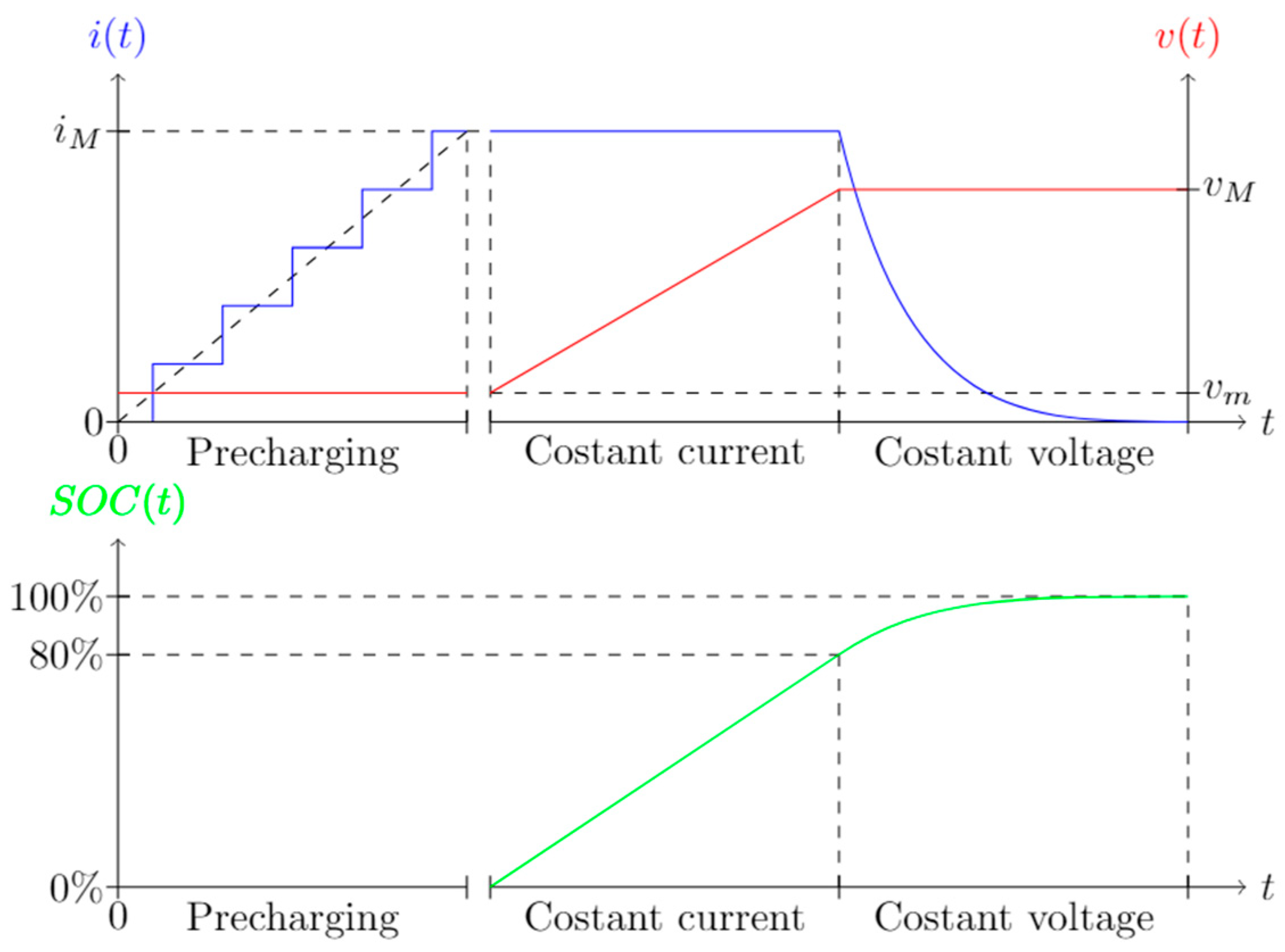
1. Introduction
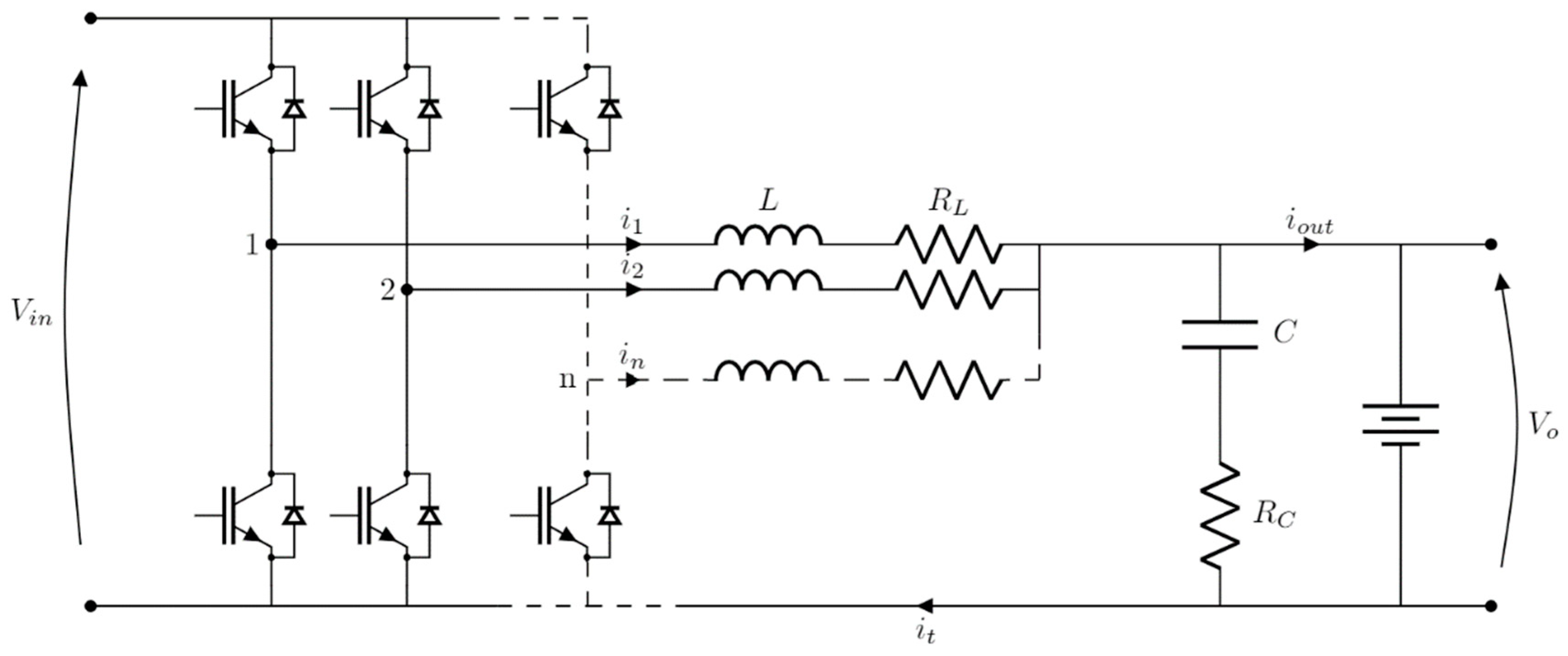
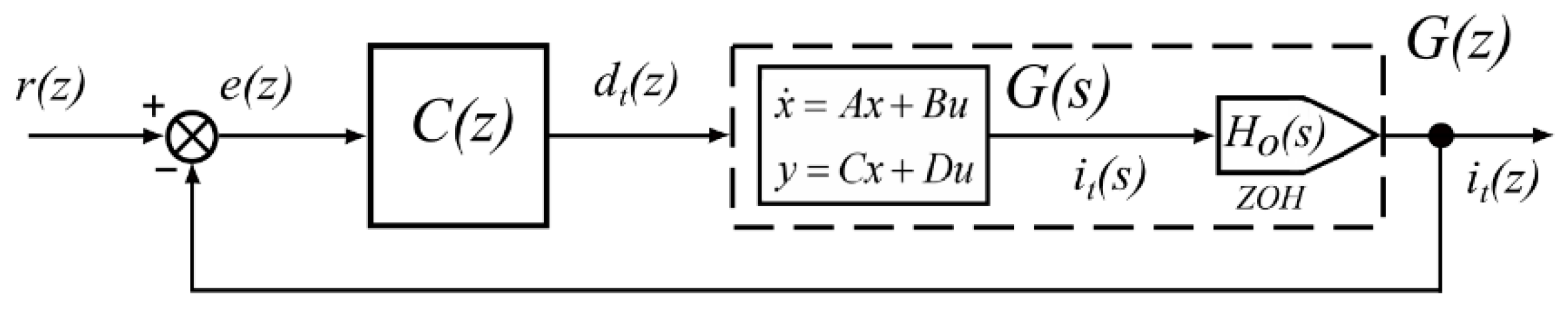
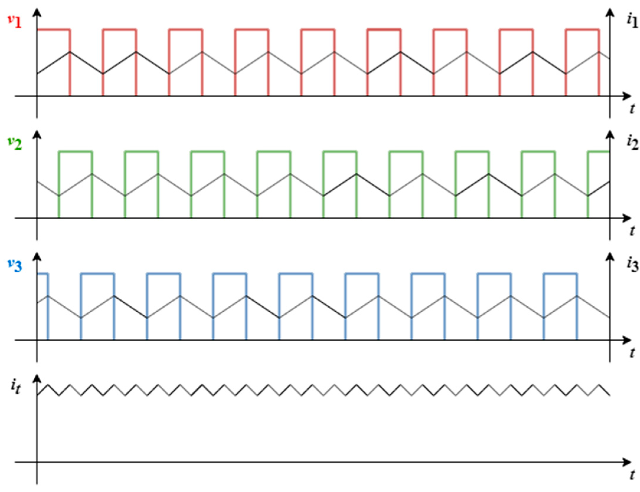
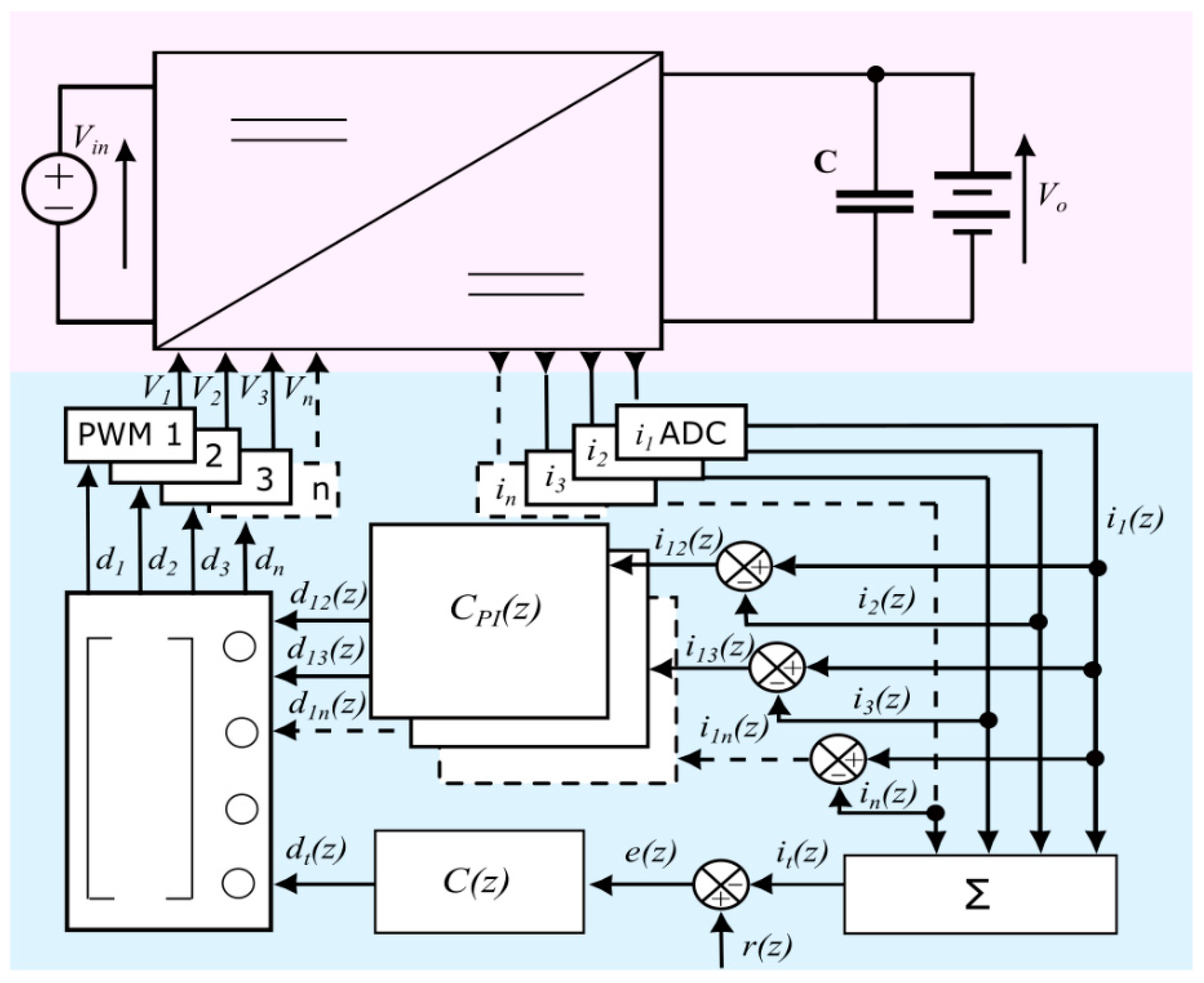
2. Continuous and Discrete-Time Model of n-Leg Interleaved Buck Converter
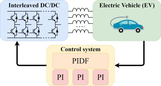
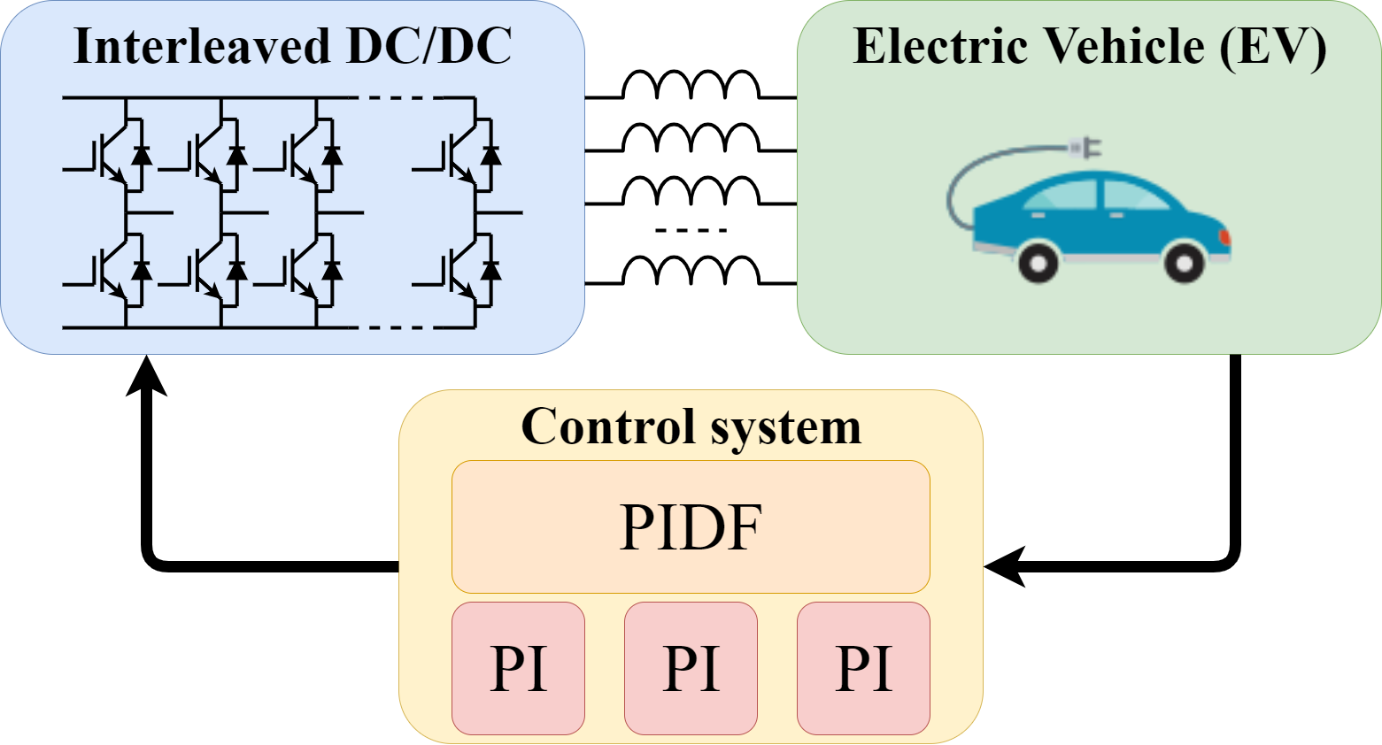
3. The Proposed Control
3.1. Average Duty Cycle Control
Control Problem
- Step 1:
- Calculate the values of ωn, ωo, ξ using (6) on the basis of the parameters of the circuit and determine the discrete transfer function G(z) using (7) and (8).
- Step 2:
- Compute the values of ωd, δd by placing the zeros of (12) in the same location of the complex conjugate poles of G(z) to cancel their detrimental effects using.
- Step 3:
- Evaluate the magnitude and the phase of the frequency response G(ej2ωTs) of the plant multiplied by the frequency response of the factor of the controller (12) that has already been determinedat the desired gain crossover frequency ωg.
- Step 4:
- Compute the magnitude and the phase that the controller should introduce to exactly satisfy the given specification on the phase margin Φm.
- Step 5:
- Calculate the values of the remaining degrees of freedom of the controller (12) using the inversion formulae.The given control problem has a feasible solution if and only if βd > 0 and > 0, see Remark 4.1 in [25].
- Step 6:
- Compute the parameters a1, a2, b0, b1, b2 using (11) to write the controller in the form (10) which is directly implementable on a microcontroller board.
3.2. Circulating Current Control
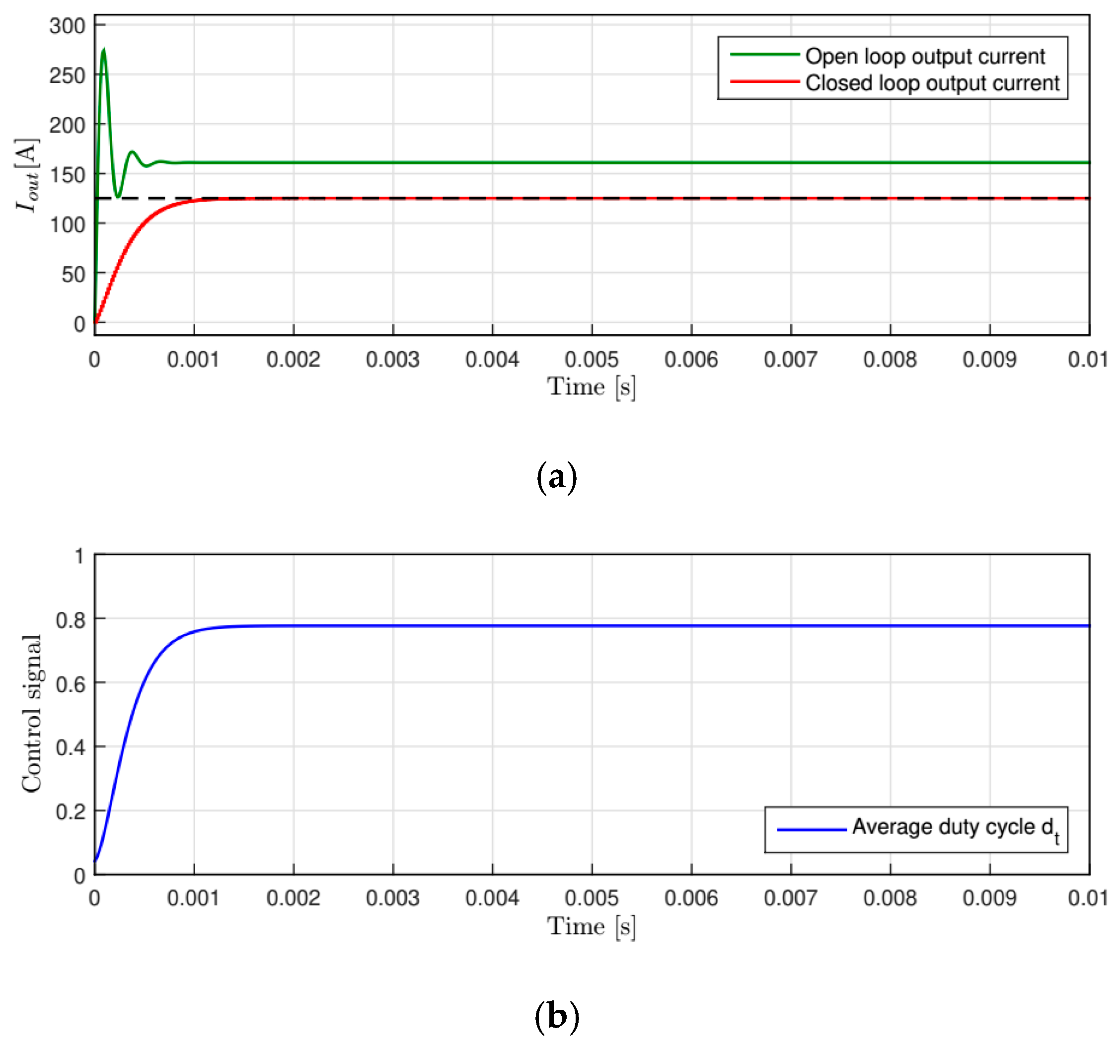
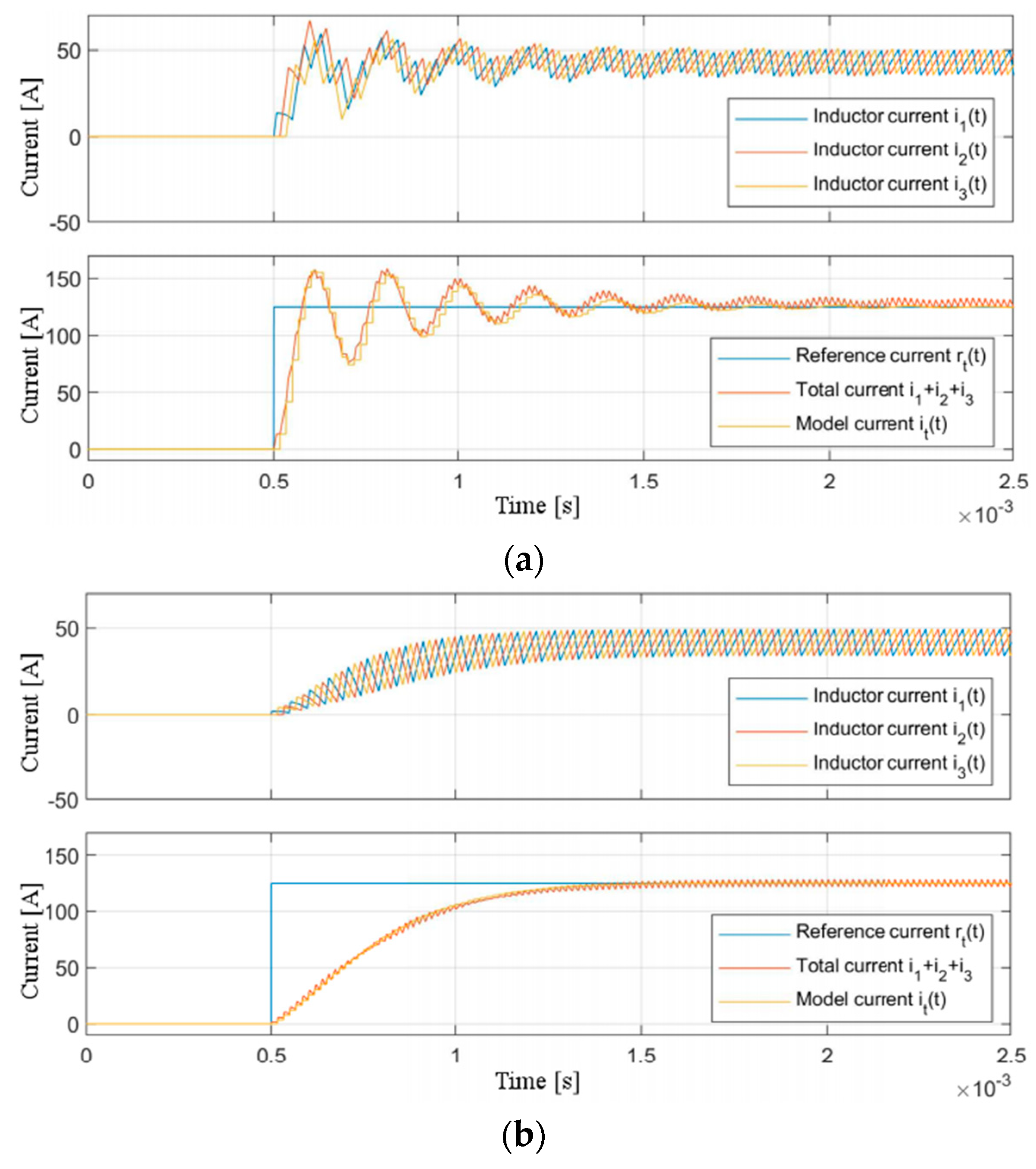
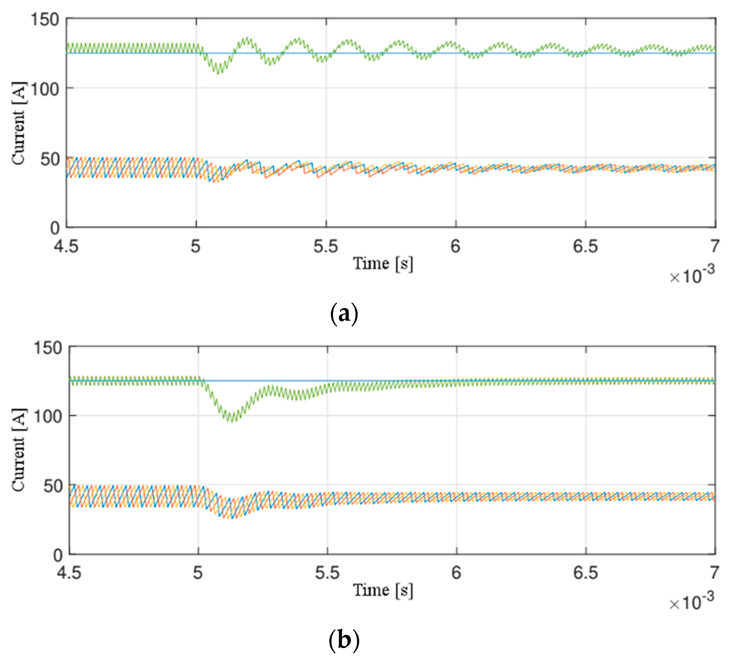
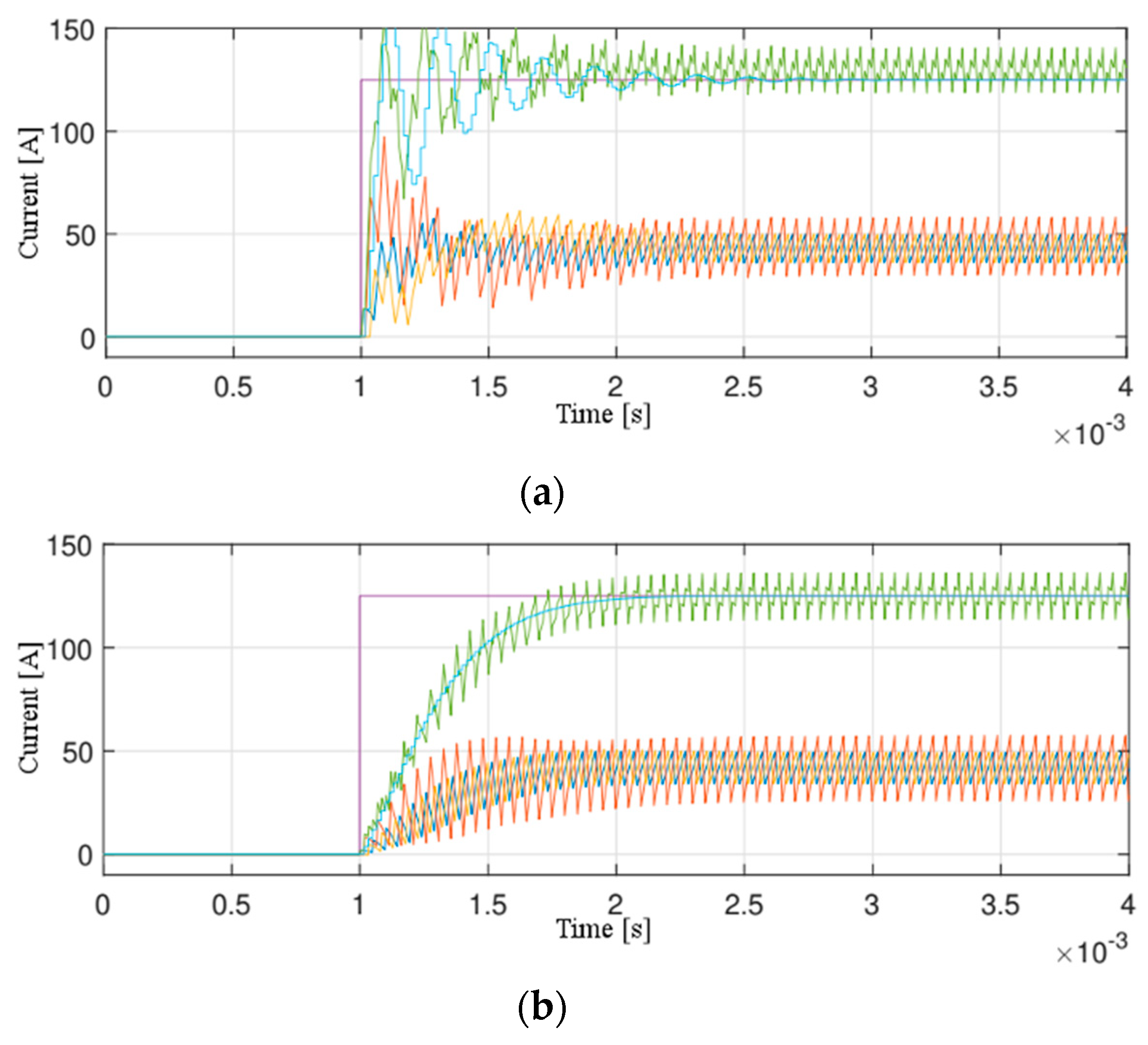
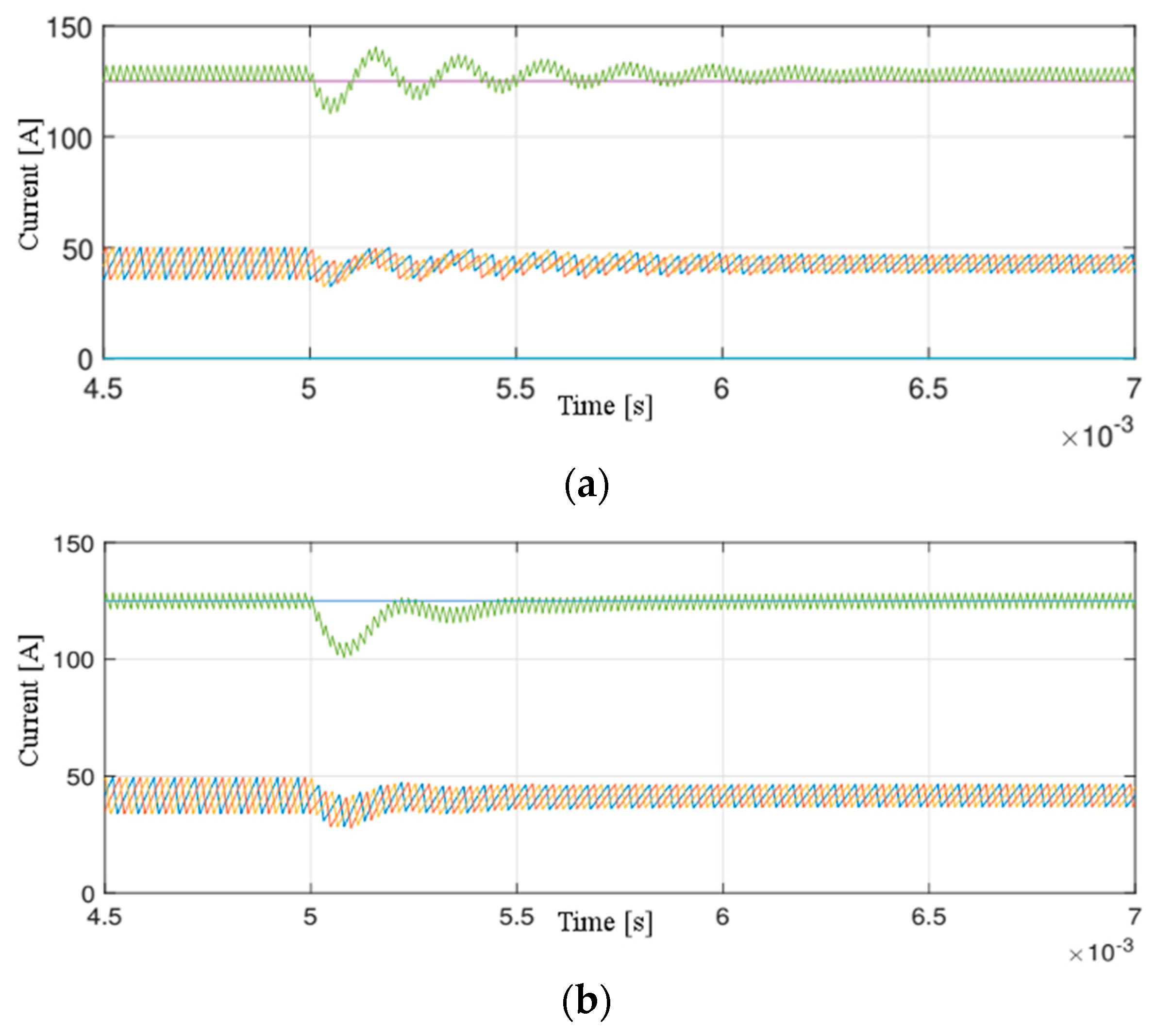
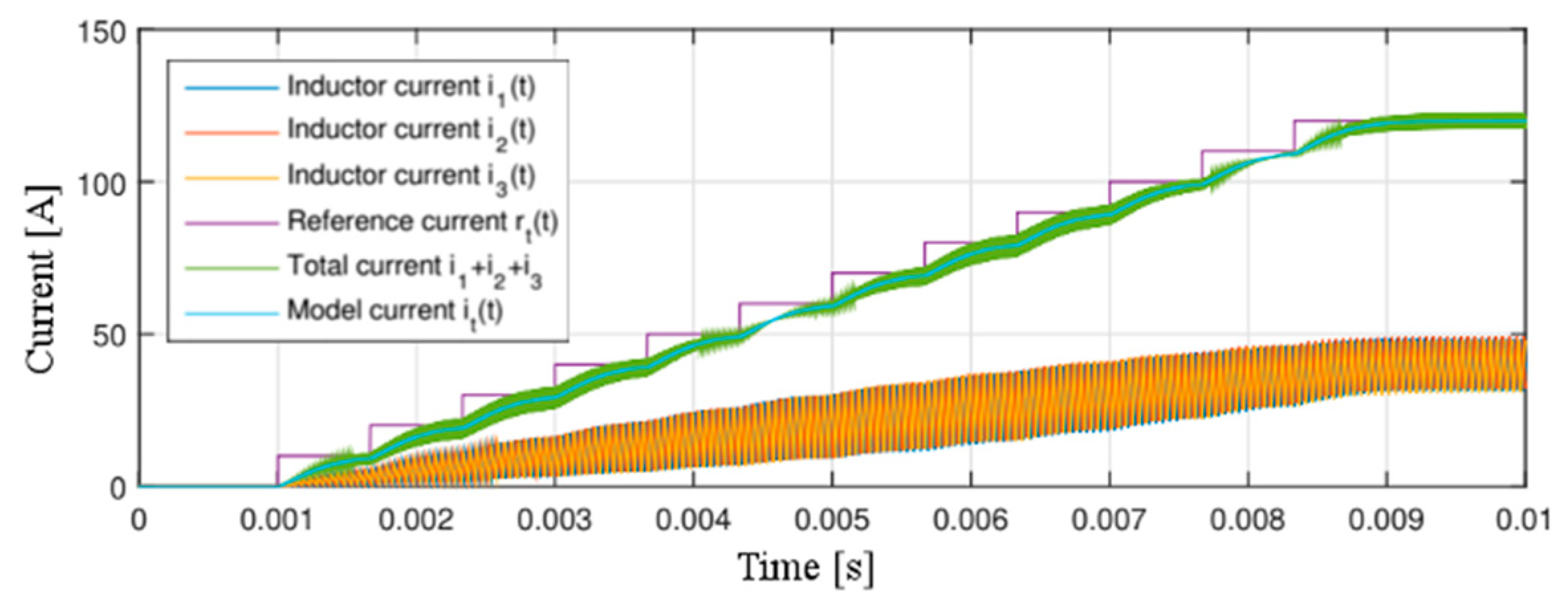
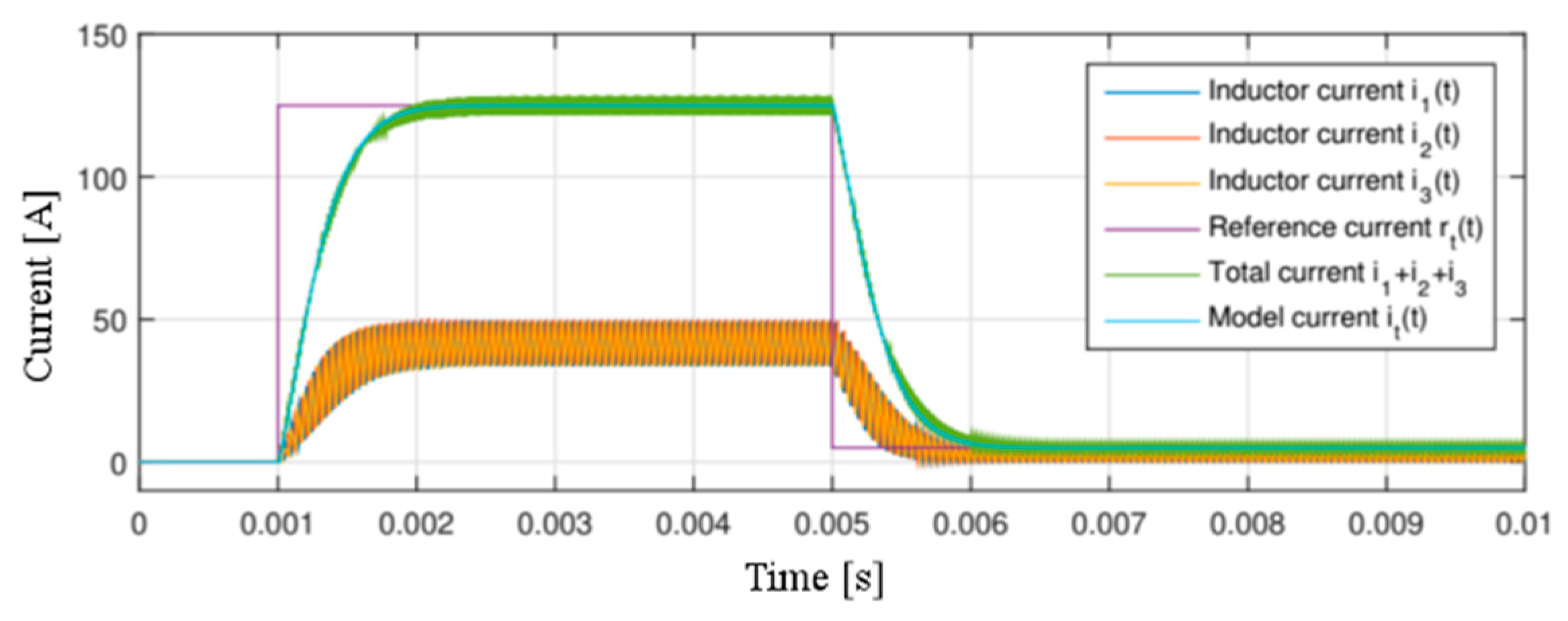
4. Numerical and Experimental Results
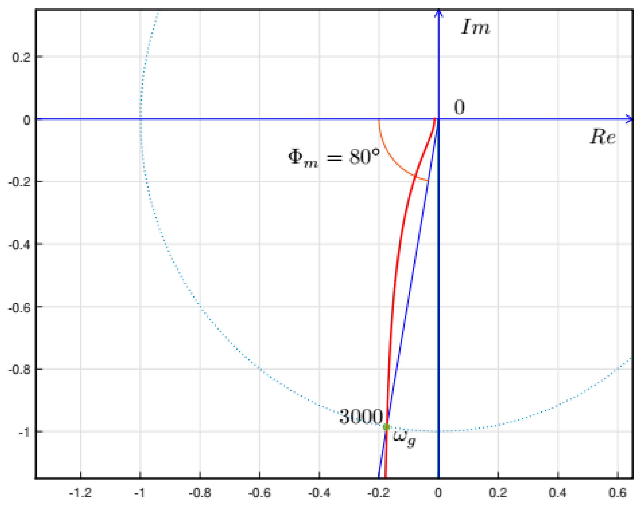
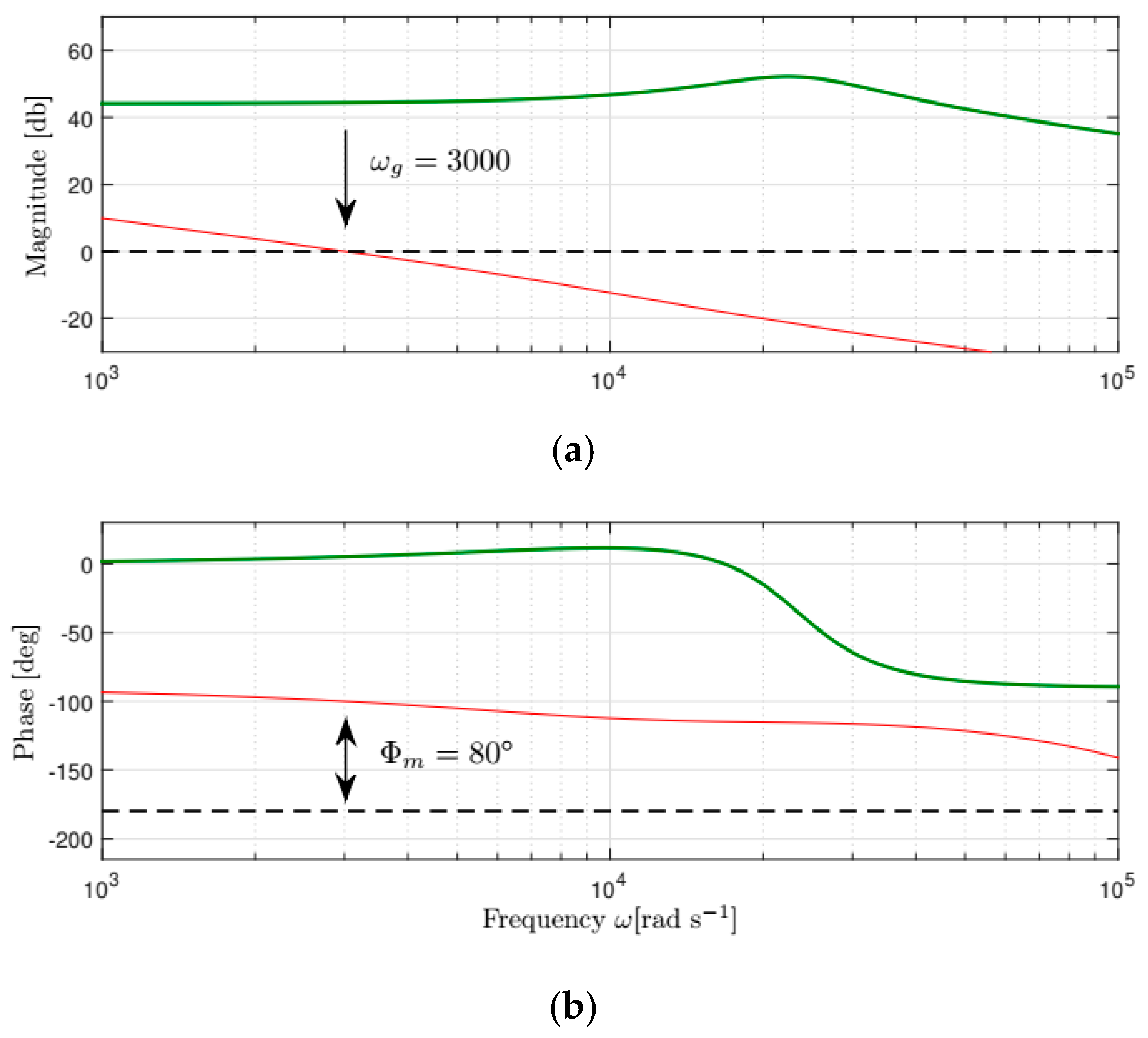
4.1. Proposed Control Procedure
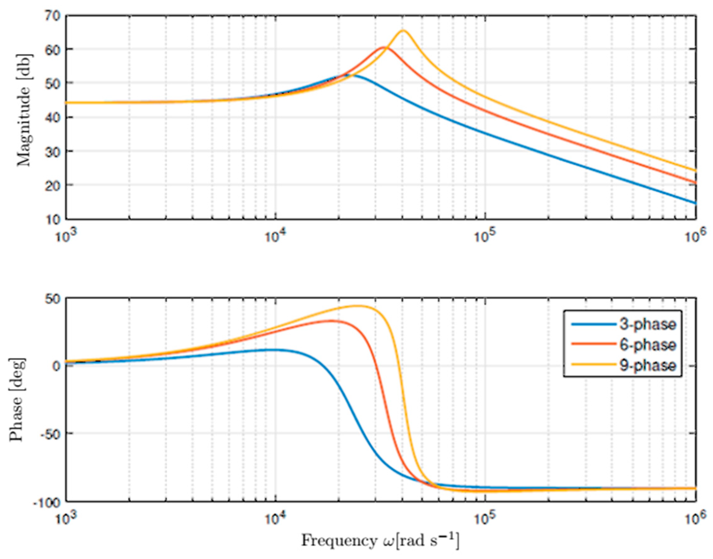
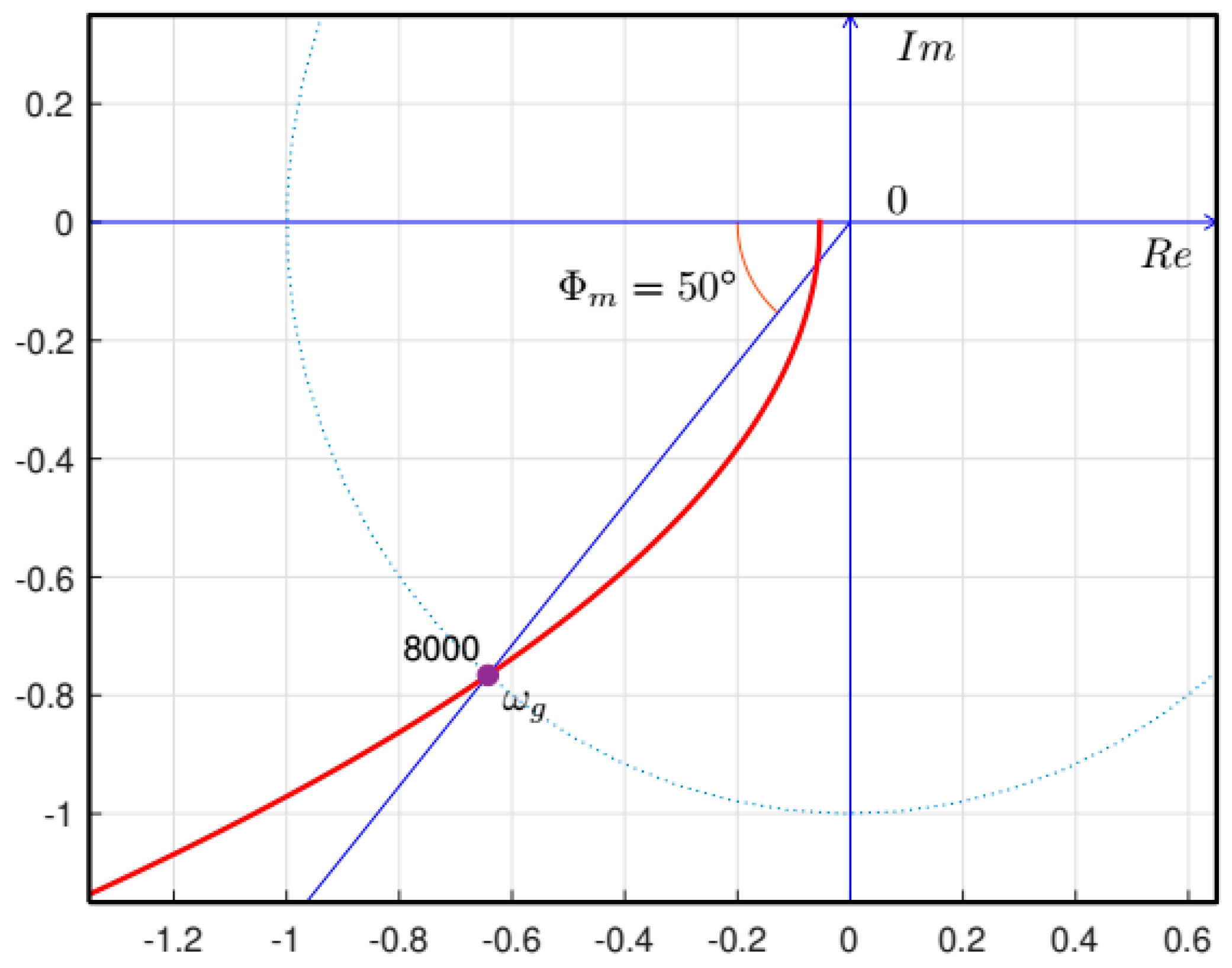
4.2. Numerical Comparison
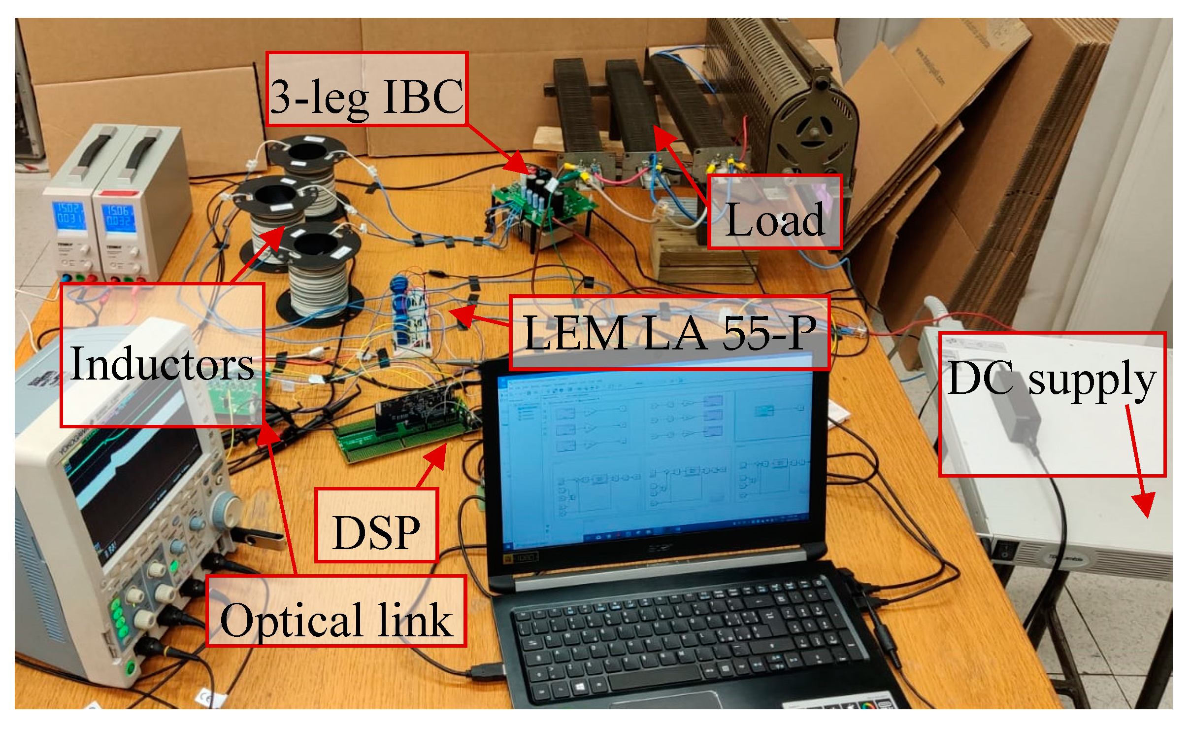
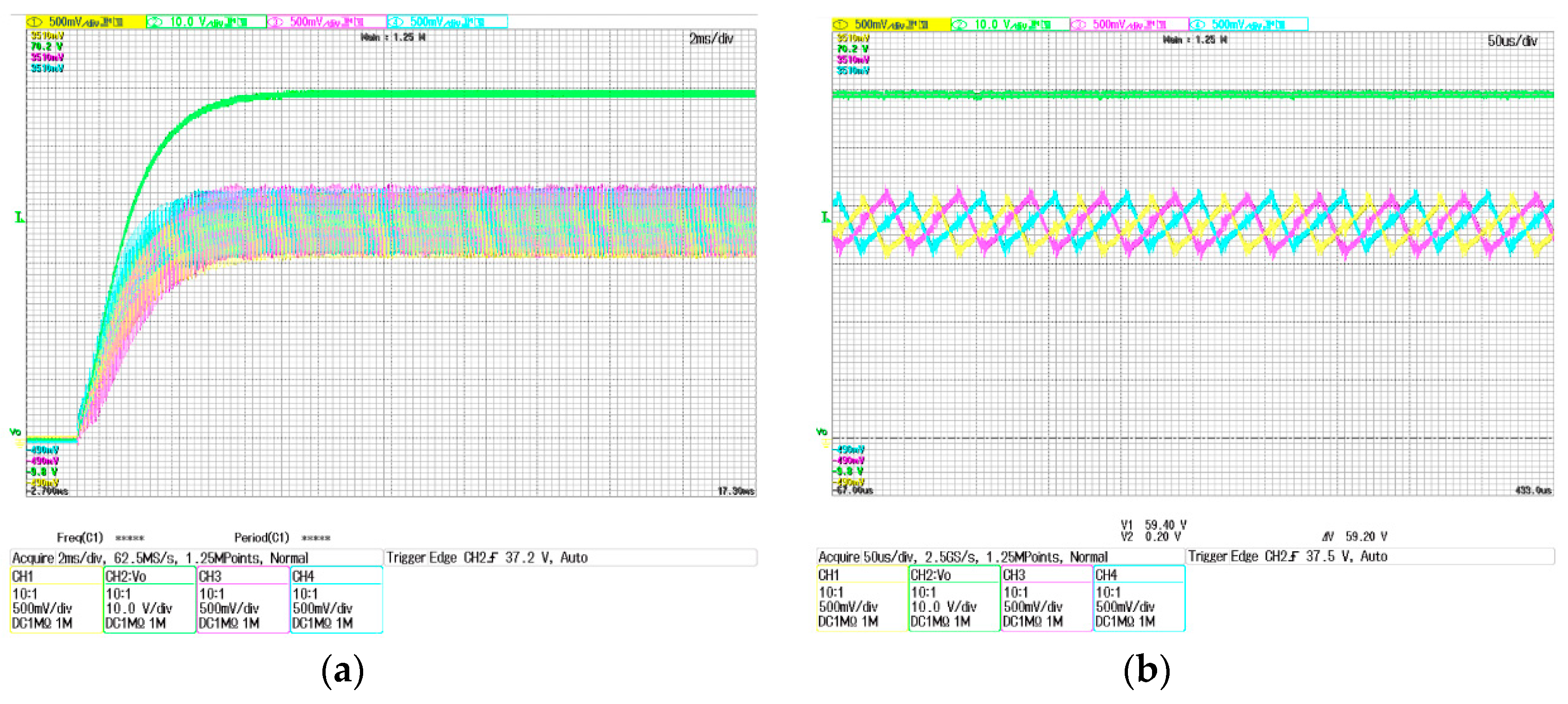
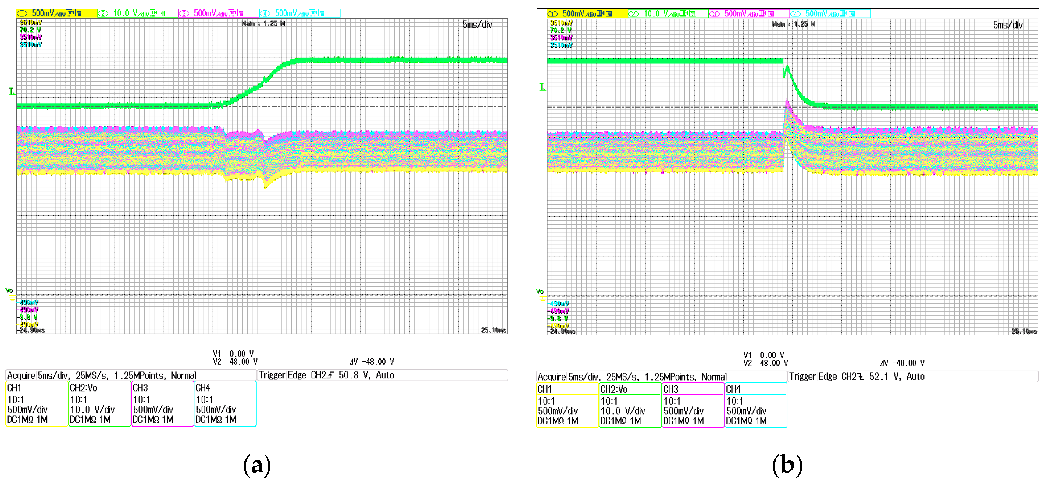
4.3. Experimental Results
5. Conclusions
Author Contributions
Funding
Conflicts of Interest
References
- Chakraborty, S.; Vu, H.-N.; Hasan, M.M.; Tran, D.-D.; Baghdadi, M.E.; Hegazy, O. DC-DC Converter Topologies for Electric Vehicles, Plug-in Hybrid Electric Vehicles and Fast Charging Stations: State of the Art and Future Trends. Energies 2019, 12, 1569. [Google Scholar] [CrossRef]
- Tan, L.; Wu, B.; Yaramasu, V.; Rivera, S.; Guo, X. Effective Voltage Balance Control for Bipolar-DC-Bus-Fed EV Charging Station With Three-Level DC–DC Fast Charger. IEEE Trans. Ind. Electron. 2016, 63, 4031–4041. [Google Scholar] [CrossRef]
- Channegowda, J.; Pathipati, V.K.; Williamson, S.S. Comprehensive review and comparison of DC fast charging converter topologies: Improving electric vehicle plug-to-wheels efficiency. In Proceedings of the 2015 IEEE 24th International Symposium on Industrial Electronics (ISIE), Buzios, Brazil, 3–5 June 2015; pp. 263–268. [Google Scholar]
- Rivera, S.; Wu, B.; Kouro, S.; Yaramasu, V.; Wang, J. Electric Vehicle Charging Station Using a Neutral Point Clamped Converter With Bipolar DC Bus. IEEE Trans. Ind. Electron. 2015, 62, 1999–2009. [Google Scholar] [CrossRef]
- Tamyurek, B.; Torrey, D.A. A Three-Phase Unity Power Factor Single-Stage AC–DC Converter Based on an Interleaved Flyback Topology. IEEE Trans. Power Electron. 2011, 26, 308–318. [Google Scholar] [CrossRef]
- Zhang, D.; Wang, F.; Burgos, R.; Lai, R.; Boroyevich, D. DC-Link Ripple Current Reduction for Paralleled Three-Phase Voltage-Source Converters with Interleaving. IEEE Trans. Power Electron. 2011, 26, 1741–1753. [Google Scholar] [CrossRef]
- Abusara, M.A.; Sharkh, S.M. Design and Control of a Grid-Connected Interleaved Inverter. IEEE Trans. Power Electron. 2013, 28, 748–764. [Google Scholar] [CrossRef]
- Jung, M.; Lempidis, G.; Holsch, D.; Steffen, J. Control and optimization strategies for interleaved dc-dc converters for EV battery charging applications. In Proceedings of the 2015 IEEE Energy Conversion Congress and Exposition (ECCE), Montreal, QC, Canada, 20–24 September 2015; pp. 6022–6028. [Google Scholar]
- Schuck, M.; Pilawa-Podgurski, R.C.N. Ripple Minimization Through Harmonic Elimination in Asymmetric Interleaved Multiphase DC–DC Converters. IEEE Trans. Power Electron. 2015, 30, 7202–7214. [Google Scholar] [CrossRef]
- Lukic, Z.; Ahsanuzzaman, S.M.; Prodic, A.; Zhao, Z. Self-Tuning Sensorless Digital Current-Mode Controller with Accurate Current Sharing for Multi-Phase DC-DC Converters. In Proceedings of the 2009 Twenty-Fourth Annual IEEE Applied Power Electronics Conference and Exposition, Washington, DC, USA, 15–19 February 2009; pp. 264–268. [Google Scholar]
- Cao, P.; Ng, W.T.; Trescases, O. Thermal management for multi-phase current mode buck converters. In Proceedings of the 2011 Twenty-Sixth Annual IEEE Applied Power Electronics Conference and Exposition (APEC), Fort Worth, TX, USA, 6–11 March 2011; pp. 1124–1129. [Google Scholar]
- Jahanbakhshi, M.-H.; Etezadinejad, M. Modeling and Current Balancing of Interleaved Buck Converter Using Single Current Sensor. In Proceedings of the 2019 27th Iranian Conference on Electrical Engineering (ICEE), Yazd, Iran, 30 April–2 May 2019; pp. 662–667. [Google Scholar]
- Balen, G.; Reis, A.R.; Pinheiro, H.; Schuch, L. Modeling and control of interleaved buck converter for electric vehicle fast chargers. In Proceedings of the 2017 Brazilian Power Electronics Conference (COBEP), Juiz de Fora, Brazil, 19–22 November 2017; pp. 1–6. [Google Scholar]
- Colvero Schittler, A.; Pappis, D.; Campos, A.; Dalla Costa, M.A.; Alonso, J.M. Interleaved Buck Converter Applied to High-Power HID Lamps Supply: Design, Modeling and Control. IEEE Trans. Ind. Appl. 2013, 49, 1844–1853. [Google Scholar] [CrossRef]
- Dorf, R.C.; Bishop, R.H. Modern Control Systems; Pearson: London, UK, 2011. [Google Scholar]
- Lee, I.-O.; Lee, J.-Y. A High-Power DC-DC Converter Topology for Battery Charging Applications. Energies 2017, 10, 871. [Google Scholar] [CrossRef]
- Drobnic, K.; Grandi, G.; Hammami, M.; Mandrioli, R.; Ricco, M.; Viatkin, A.; Vujacic, M. An Output Ripple-Free Fast Charger for Electric Vehicles Based on Grid-Tied Modular Three-Phase Interleaved Converters. IEEE Trans. Ind. Appl. 2019, 55, 6102–6114. [Google Scholar] [CrossRef]
- Florides, M. Interleaved Switching of DC/DC Converters. Master’s Thesis, Newcastle University, Newcastle upon Tyne, UK, January 2010. [Google Scholar]
- Guo, L.Y.; Hung, J.Y.; Nelms, R.M. PID controller modifications to improve steady-state performance of digital controllers for buck and boost converters. In Proceedings of the APEC. Seventeenth Annual IEEE Applied Power Electronics Conference and Exposition, Dallas, TX, USA, 10–14 March 2002; pp. 381–388. [Google Scholar]
- Cuoghi, S.; Ntogramatzidis, L.; Padula, F.; Grandi, G. Direct Digital Design of PIDF Controllers with Complex Zeros for DC-DC Buck Converters. Energies 2018, 12, 36. [Google Scholar] [CrossRef]
- Marro, G.; Zanasi, R. New formulae and graphics for compensator design. In Proceedings of the 1998 IEEE International Conference on Control Applications (Cat. No.98CH36104), Trieste, Italy, 4 September 1998; pp. 129–133. [Google Scholar]
- Ntogramatzidis, L.; Ferrante, A. Exact Tuning of PID Controllers in Control Feedback Design. IFAC Proc. Vol. 2011, 44, 5759–5764. [Google Scholar] [CrossRef]
- Cuoghi, S.; Ntogramatzidis, L. Direct and exact methods for the synthesis of discrete-time proportional–integral–derivative controllers. IET Control Theory Appl. 2013, 7, 2164–2171. [Google Scholar] [CrossRef]
- Middlebrook, R.D.; Cuk, S. A general unified approach to modelling switching-converter power stages. In Proceedings of the 1976 IEEE Power Electronics Specialists Conference, Cleveland, OH, USA, 8–10 June 1976; pp. 18–34. [Google Scholar]
- Ito, Y.; Yang, Z.; Akagi, H. DC micro-grid based distribution power generation system. In Proceedings of the Conference Proceedings—IPEMC 2004: 4th International Power Electronics and Motion Control Conference, Xi’an, China, 14–16 August 2004; Volume 3, pp. 1740–1745. [Google Scholar]
- Adrees, A.; Andami, H.; Milanovic, J.V. Comparison of dynamic models of battery energy storage for frequency regulation in power system. In Proceedings of the 2016 18th Mediterranean Electrotechnical Conference (MELECON), Lemesos, Cyprus, 18–20 April 2016; pp. 1–6. [Google Scholar]
- Emadi, A.; Khaligh, A.; Rivetta, C.H.; Williamson, G.A. Constant Power Loads and Negative Impedance Instability in Automotive Systems: Definition, Modeling, Stability, and Control of Power Electronic Converters and Motor Drives. IEEE Trans. Veh. Technol. 2006, 55, 1112–1125. [Google Scholar] [CrossRef]
- Wong, K. Output Capacitor Stability Study on a Voltage-Mode Buck Regulator Using System-Poles Approach. IEEE Trans. Circuits Syst. II 2004, 51, 436–441. [Google Scholar] [CrossRef]


| Label | Description | Case (a) Simulations | Case (b) Experiments |
|---|---|---|---|
| n | Number of legs | 3 | 3 |
| Vin | DC-input nominal voltage | 618 V | 90 V |
| Iref | Output reference current | 125 A | 10 A |
| fsw, fs | Switching and sampling frequencies | 20 kHz, 60 kHz | 20 kHz, 60 kHz |
| A/D | Converter resolution | 12 bits | 12 bits |
| RL, L | Coupling resistance and inductance | 0 Ω, 0.344 mH | 0.91 Ω, 0.99 mH |
| C | Capacitance | 16 µF | 13.5 µF |
| R | Load | [0.10–3.84] Ω | [0.10–5.94] Ω |
© 2020 by the authors. Licensee MDPI, Basel, Switzerland. This article is an open access article distributed under the terms and conditions of the Creative Commons Attribution (CC BY) license (http://creativecommons.org/licenses/by/4.0/).
Share and Cite
Cuoghi, S.; Mandrioli, R.; Ntogramatzidis, L.; Gabriele, G. Multileg Interleaved Buck Converter for EV Charging: Discrete-Time Model and Direct Control Design. Energies 2020, 13, 466. https://doi.org/10.3390/en13020466
Cuoghi S, Mandrioli R, Ntogramatzidis L, Gabriele G. Multileg Interleaved Buck Converter for EV Charging: Discrete-Time Model and Direct Control Design. Energies. 2020; 13(2):466. https://doi.org/10.3390/en13020466
Chicago/Turabian StyleCuoghi, Stefania, Riccardo Mandrioli, Lorenzo Ntogramatzidis, and Grandi Gabriele. 2020. "Multileg Interleaved Buck Converter for EV Charging: Discrete-Time Model and Direct Control Design" Energies 13, no. 2: 466. https://doi.org/10.3390/en13020466
APA StyleCuoghi, S., Mandrioli, R., Ntogramatzidis, L., & Gabriele, G. (2020). Multileg Interleaved Buck Converter for EV Charging: Discrete-Time Model and Direct Control Design. Energies, 13(2), 466. https://doi.org/10.3390/en13020466