Article

A Topology Synthetization Method for Single-Phase, Full-Bridge, Transformerless Inverter with Leakage Current Suppression Part I

1
College of Electrical and Information Engineering, Hunan University, Changsha 410082, China
2
Department of Electrical and Computer Engineering, Queen’s University, Kingston, ON K7L 3N6, Canada
*
Author to whom correspondence should be addressed.
Energies 2020, 13(2), 434; https://doi.org/10.3390/en13020434
Submission received: 23 November 2019 / Revised: 7 January 2020 / Accepted: 10 January 2020 / Published: 16 January 2020

Abstract

:
Single-phase full-bridge transformerless topologies, such as the H5, H6, or the highly efficient and reliable inverter concept (HERIC) topologies, are commonly used for leakage current suppression for photovoltaic (PV) applications. The main derivation methodology of full-bridge topologies has been used based on both a DC-based decoupling model and an AC-based decoupling model. However, this methodology is not suited to the search for all possible topologies, and cannot verify whether they are inclusive. Part I of this paper will propose a new topology derivation methodology based on unipolar sinusoidal pulse width modulation (USPWM) to search all possible full-bridge topologies for leakage current suppression. First of all, a unified circuit model is proposed, instead of the DC- and AC-based models. Secondly, a mathematic method called the MN principle is then proposed to search for all possible topologies, and a derivation procedure is provided. It was verified that all existing topologies could be found using the proposed method; furthermore, seven new topologies were derived. The proposed topology derivation methodology is extended to search topologies under Double-Frequency USPWM (DFUSPWM). Twenty topologies under USPWM and four topologies under DFUSPWM have been derived.

Graphical Abstract

1. Introduction

Photovoltaic (PV) sources are among the most promising renewable energy sources, providing clean and emission free energy [1,2]. The single-phase transformerless inverter system has popularly been used, as it has high efficiency and low cost compared with the transformer inverter system. However, the leakage current is a key issue [3,4,5]. The leakage current generated by PV parasitic capacitors must be limited to satisfy the VDC-AR_N 4015 [6], UL1741 [7], and VDE 0126-1-1 [8] standards. In single-phase, grid-tied inverter systems, half-bridge and full-bridge inverters are typical topologies, as shown in Figure 1.
The Common Mode (CM) current path for grid-tied, transformerless, PV inverter systems is illustrated in Figure 2 [9]. The leakage current path is equivalent to an LC resonant circuit, as shown in Figure 3 [10,11]. VAN and VBN are the voltage difference between points A and N and points B and N, respectively, and L1 and L2 are the output filter inductors. The equivalent CM voltage Vecm is defined as:
V ecm = V AN + V BN 2 + V AN V BN 2 L 2 L 1 L 2 + L 1
For the half-bridge inverter in Figure 1a, only the output filter inductor L1 is employed, so L2 = 0. Thus, (1) can be simplified as follows:
V ecm = V AN + V BN 2 + V AN V BN 2 = V BN
In Figure 1a, two capacitors, Cdc1 and Cdc2, with equal capacitance values are in series. Capacitor Cdc2 is charged or discharged by the grid current, and voltage VBN equals half of the input voltage plus the voltage fluctuation of the line frequency. But the high-frequency fluctuation is so small that it can be ignored. So, VBN is approximately constant. However, the DC voltage utilization of half-bridge inverters is only half that of full-bridge topologies, which means that a high-gain boost converter is needed as the first stage. As such, system efficiency and cost will be adversely affected. When two filter inductors are employed (L1 = L2), equation (1) can be simplified as:
V ecm = V AN + V BN 2 0 = V AN V BN 2
For the full-bridge topology, the leakage current can be eliminated if the common voltage is kept constant. Some state-of-the-art topologies such as H5 [12], HERIC [13,14], and H6 [10,15,16,17,18,19,20,21,22,23,24,25,26,27,28,29,30,31,32,33,34,35,36,37,38,39,40,41,42,43] have been developed. However, there is still a small leakage current because of the parasitic parameters. Thus, the Neutral Point Clamped (NPC) technique is introduced to achieve zero leakage current [44,45,46,47,48]. The full-bridge topologies are divided into DC decoupling model and AC decoupling model [49].
A few rules have been indirectly reported in the literature, as well as some topology synthetization methods such as those based on the DC- and AC-decoupling model, as well as topology derivation methods from H4, H5, and H6. None of the topology synthetization methods currently being used could answer the question of how many topologies could be derived, as there is no unified model. Part I of this paper focus on the topology derivation methodology to achieve small leakage current [50]. It proposes a unified model to replace the DC- and AC-decoupling models based on four rules, including two which have already been reported in the literature [51,52]. More importantly, a mathematic method called the “MN principle” is proposed to derive all the possible topologies. This only focuses on the number of switches in PC and NC modes. The MN principle also verifies that we only need to focus on M ≤ 4, N ≤ 4, because the remaining topologies can always be simplified into one of them. Thus, the method verifies that all possible topologies can be found. The derivation procedures are introduced to determine all the existing topologies and new topologies under unipolar sinusoidal pulse width modulation (USPWM) and Double-Frequency USPWM (DFUSPWM).
Part I of the paper is organized as follows. Section 2 describes the principles of the unified topology model. Section 3 introduces topology derivation under USPWM. The topology derivation under DFUSPWM is introduced in Section 4. Part I of the paper is concluded in Section 5.

2. Principle of Unified Topology Model and Symmetric Methodology

Figure 4 shows the full-bridge topology and a simplified schematic diagram.
In Figure 4a, point P and point N indicate the positive and negative DC bus terminals, respectively, and point A and point B indicate the first and second arm terminals, respectively. The semiconductor switches are always used to connect or disconnect points P and N to points A and B. Figure 4b shows a simplified schematic diagram of the full-bridge topology. Switches TPA, TNA, TPB, and TNB are the equivalent switches between points P and A, between N and A, between P and B, and between N and B, respectively. It should be noted that each equivalent switch can be a single active switch or several active switches connected in series. VPN is the input voltage. The number of switches between points P and A is X1, between points B and N is X2, between points P and B is Y1, and between points N and A is Y2.

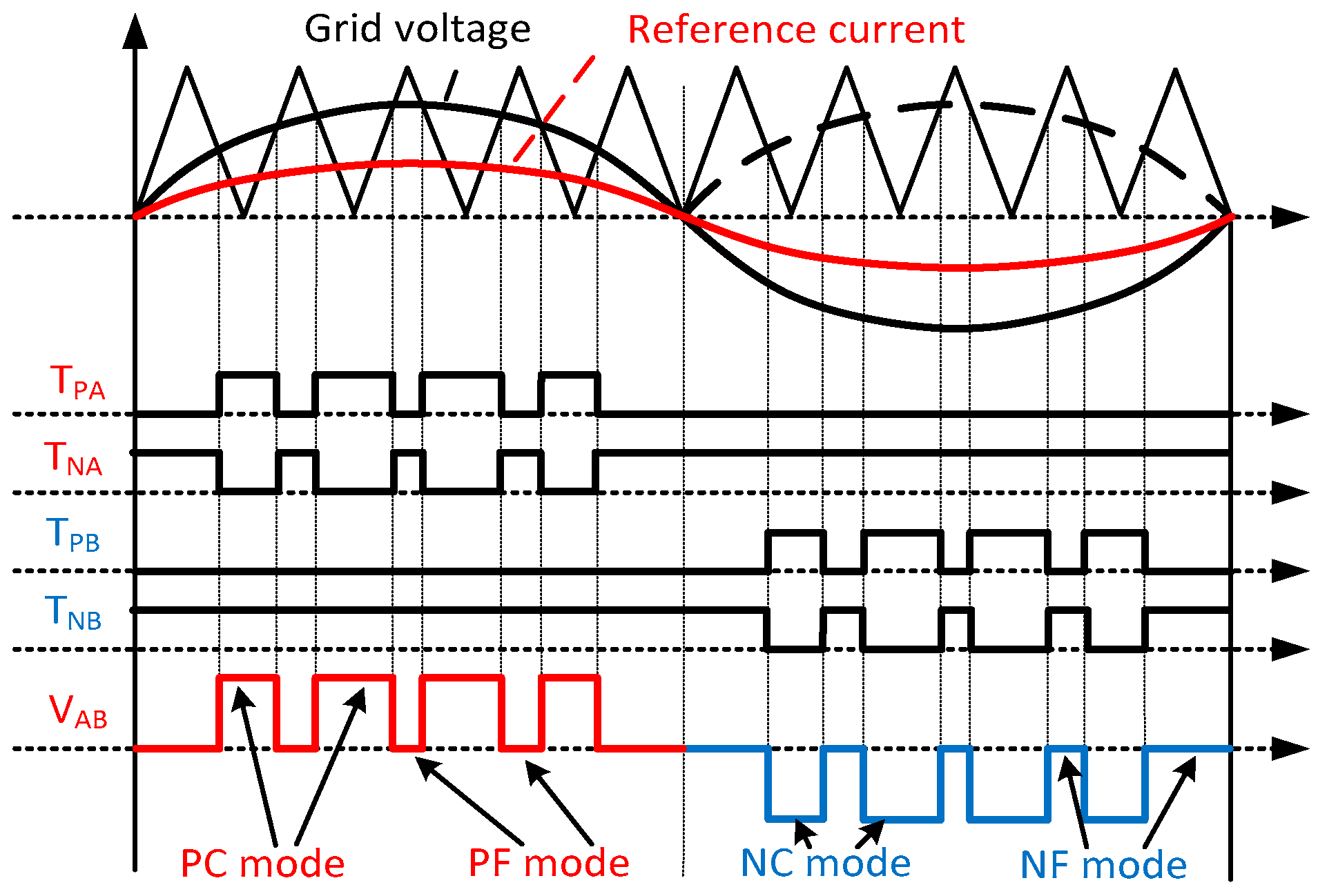
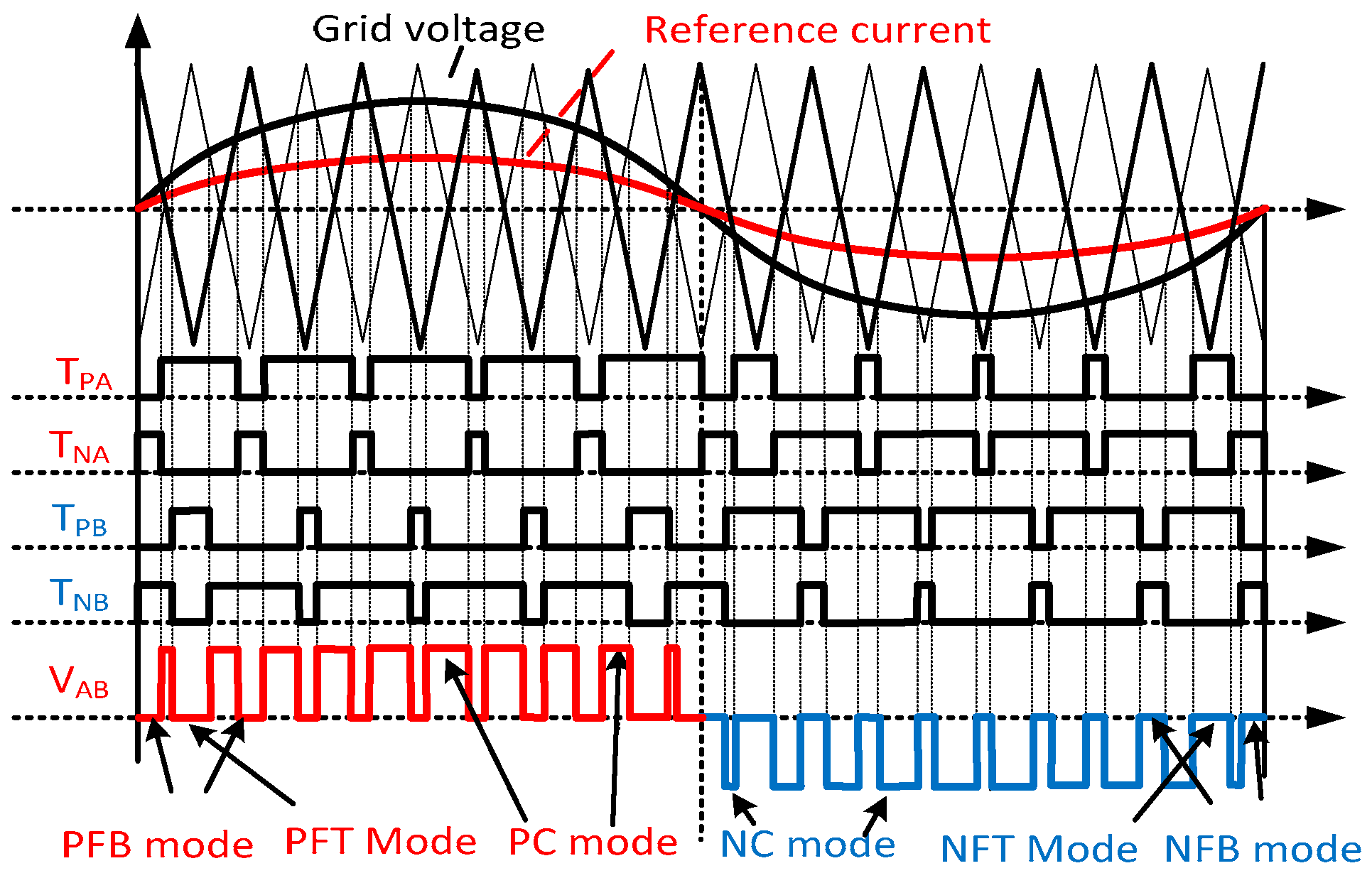
2.1. Principle of USPWM

Figure 5 shows the principle of USPWM. The differential-mode voltage VAB has three levels: +VPN, 0, and −VPN. There are four modes in a total line-frequency period. The inverter is working in positive conduction (PC) mode and negative conduction (NC) mode when VAB equals to +VPN and −VPN. There are two modes if VAB = 0: one is the positive freewheeling (PF) mode when the grid current is positive, and the other is the negative freewheeling (NF) mode when the grid current is negative.

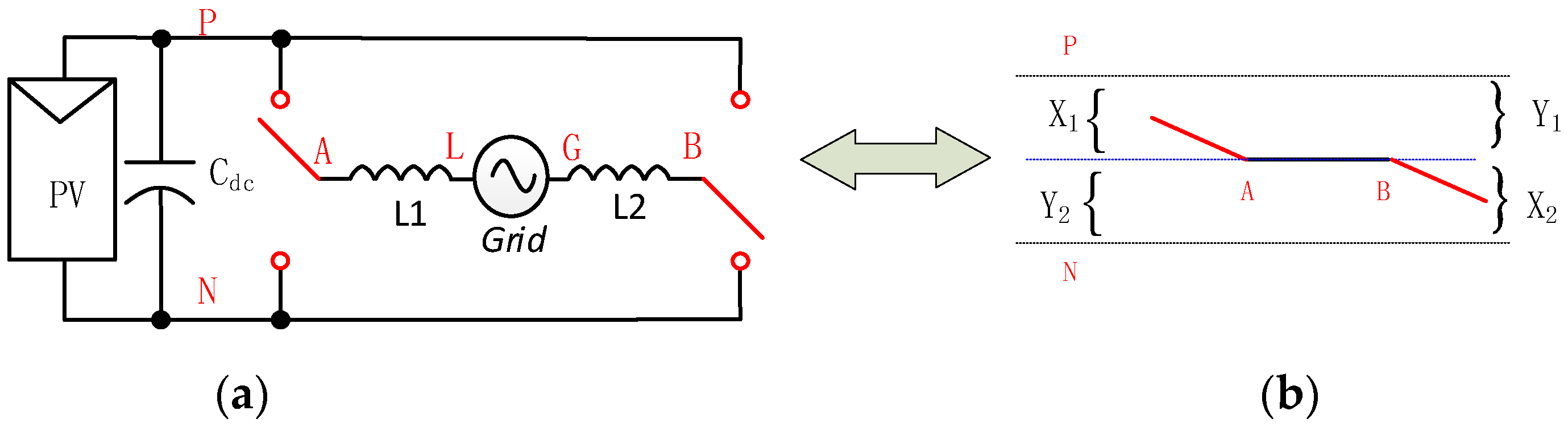
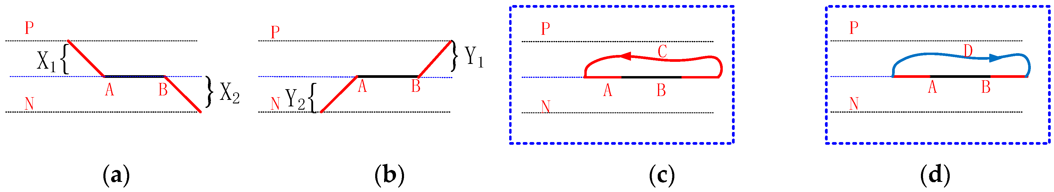
2.2. Unified Topology Model
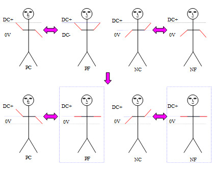
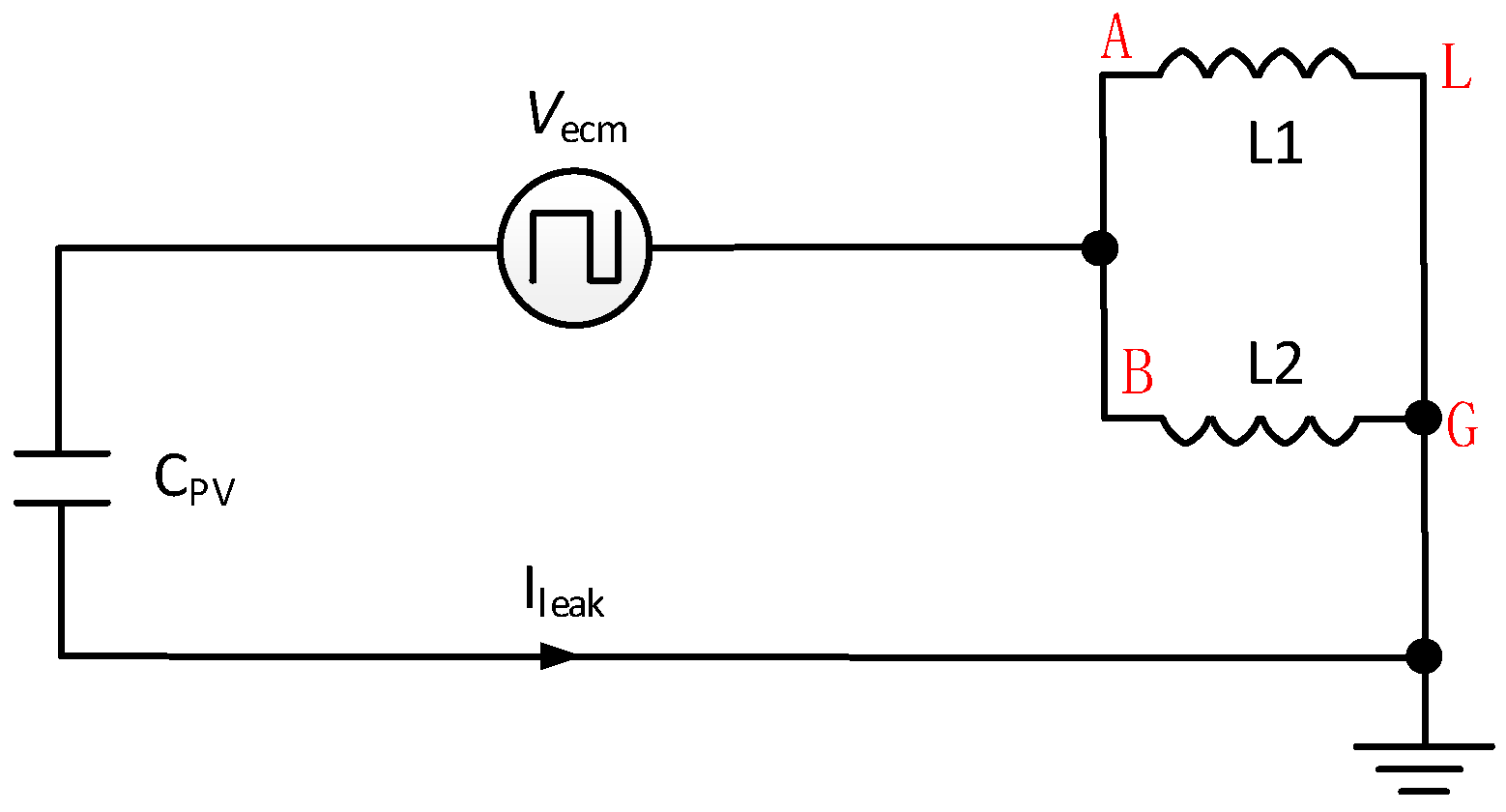
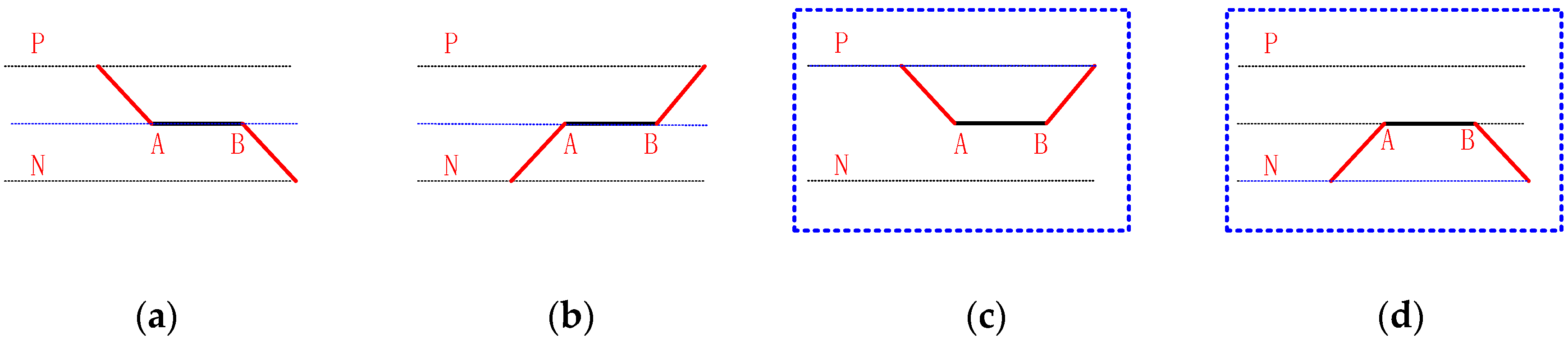
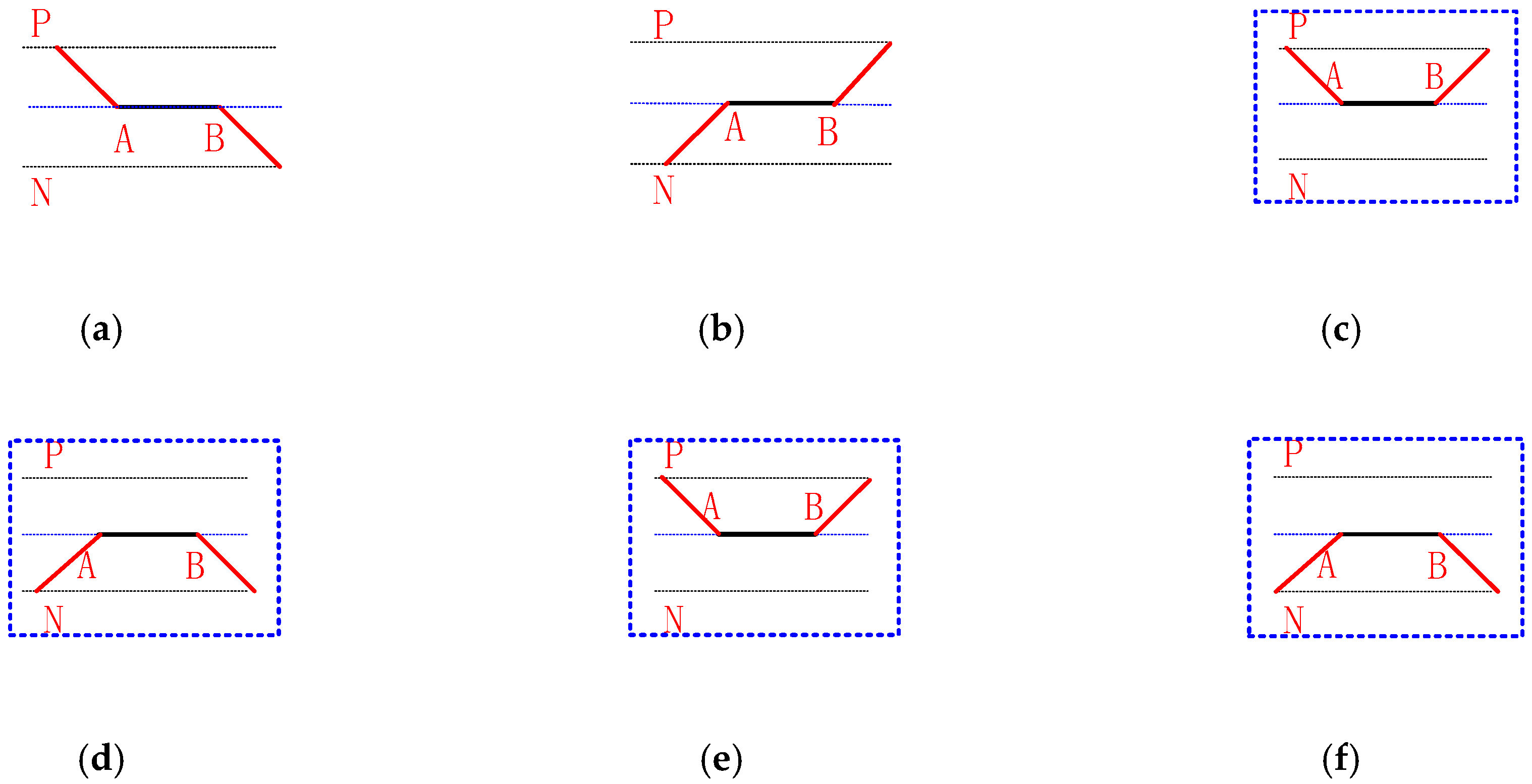
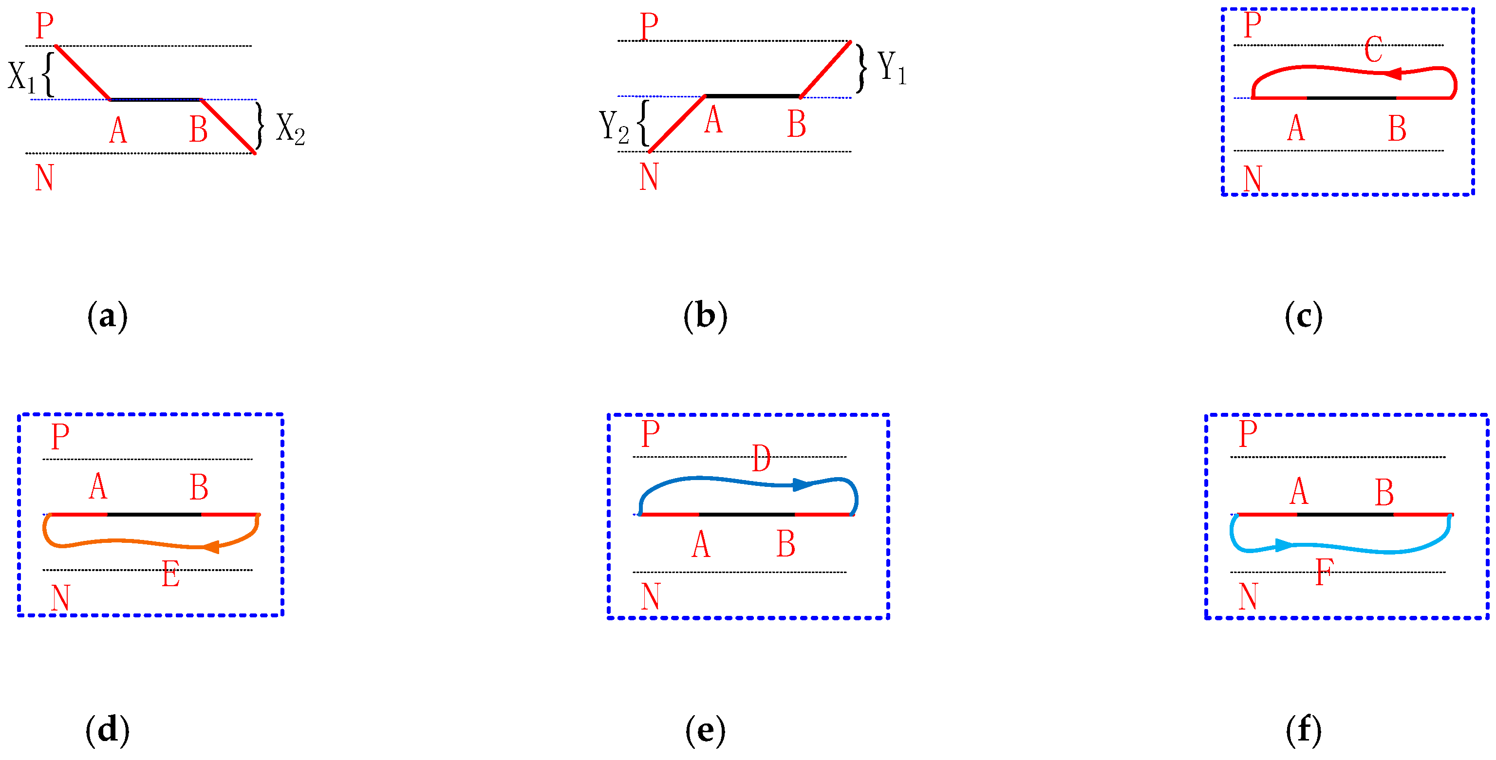
Figure 6 shows four modes under USPWM based on the conventional H4 full-bridge topology. As shown in (4), the CM voltage, Vcm, is half the input voltage in PC and NC modes, equaling either input voltage VPN or zero in PF mode and NF mode.
The CM voltage is not constant at switching frequency, which results in high-frequency leakage current.
V cm = V AN + V BN 2 = { = V PN 2      PC   mode   or   NC   mode = V PN   or   0 PC   mode   or   NC   mode
To minimize the leakage current, the CM voltage must be kept constant. In PC and NC modes, the CM voltage is equal to half of the DC voltage. Thus, the main objective is to keep the CM voltage also being clamped to half of the input voltage in both freewheeling modes (PF and NF).
V cm = V AN + V BN 2 = { = V PN 2    PC   mode   or   NC   mode V PN 2    PC   mode   or   NC   mode
A unified topology model in PF and NF modes, as shown in Figure 7, is proposed [50]. All switches that connect points P and N are off. A controllable branch BCA ^ is added to flow positive current in PF mode, as shown in Figure 7c, and another controllable branch ADB ^ flowing negative current is added in NF mode in Figure 7d. The voltage VAB = 0 in PF and NF modes. To regulate the leakage current, a unified topology model should be constructed according to the following four rules in PF and NF modes:
Rule #1. Turn off all the connections to points P and N.
All switches connected to the positive DC bus (point P) and the negative DC bus (point N) must be off in the PF and NF intervals.
Rule #2. Short-circuit terminals A and B to get VAB = 0.
A, B is short-circuited through one controllable branch in PF and NF modes. One switch and one diode connected in series are used for bidirectional voltage stress and output current flow, respectively. For example, switch TPF and diode DPF are connected in series for positive current flowing from point B to point A. Switch TNF and diode DNF are connected in series for negative current flowing from point A to point B.
Rule #3. Low cost implementation to satisfy Rule #2.
For low cost, the switches which are not connected to points P and N are on to provide output current flow path in PF and NF modes.
Rule #4. Combine PF and NF modes, and cut off the redundant components.
One PF mode and one NF mode implementation are combined to form a topology. The components which are connected in parallel are merged into one as best as they can be. For example, if an extra diode is connected in parallel with the body-diode of a switch, the former is saved to reduce cost, i.e., two switches in parallel are replaced by one switch.
Based on these rules, a systematic methodology called the “MN principle” is proposed, and will be discussed in the following subsection.

2.3. MN Principle

A systematic methodology, the MN principle, is proposed to derive all possible full-bridge topologies with small leakage currents. The MN principle can be described as follows. Let M denote the total number of switches that are turned on in PC mode. Since X1 is the number of switches that connect point P to point A in PC mode, and X2 is the number of switches that connect point B to point N in PC mode, then
M = X 1 + X 2
Similarly, let N denote the total number of switches that are turned on in NC mode. Since Y1 is the number of switches that connect point P to point B and Y2 is the number that connect point A to point N in NC mode, then
N = Y 1 + Y 2
According to rule #1, points A and B must be disconnected to points P and N, which means that at least one switch is needed for TPA, TNB, TPB, and TNA. Thus, the minimum values of X1, X2, Y1, and Y2 should be one, as shown in (8).
M i n ( X 1 , X 2 , Y 1 , Y 2 ) 1
In order to disconnect A, B to P, N in PF and NF modes, according to rule #2, one switch and an extra diode connected in series can be used. Thus, there is one possible way that two switches are in series to implement the equivalent switches TPA, TNB, TPB, and TNA, respectively. For example, two switches, TP1 and TP2, are connected in series between points P and A to implement the equivalent switch, i.e., TPA. Switch TP1 remains off to disconnect points P and A, and switch TP2 remains on to construct the freewheeling branch in PF mode. If three switches, TP1, TP2, and TP3, are in series to implement the equivalent switch TPA, switch TP1 remains off to disconnect points P and A, and two switches TP2 and TP3 are in series to construct the freewheeling branch in PF mode. However, the two switches, TP2 and TP3, can be merged into a single switch. Thus, the maximum value for X1, X2, Y1, and Y2 are less than or equal to 2. Therefore,
M a x ( X 1 , X 2 , Y 1 , Y 2 ) 2
From the above analysis, it may be observed that the MN principle can cover all possible topologies. Some of them can be simplified. Thus, only simplified topologies are introduced in the next section.

3. Topology Derivation under USPWM

In this section, several examples are provided to show how to derive topologies from the MN principle, such as M = 2 and N = 2, M = 2 and N = 3, or M = 3 and N = 2.

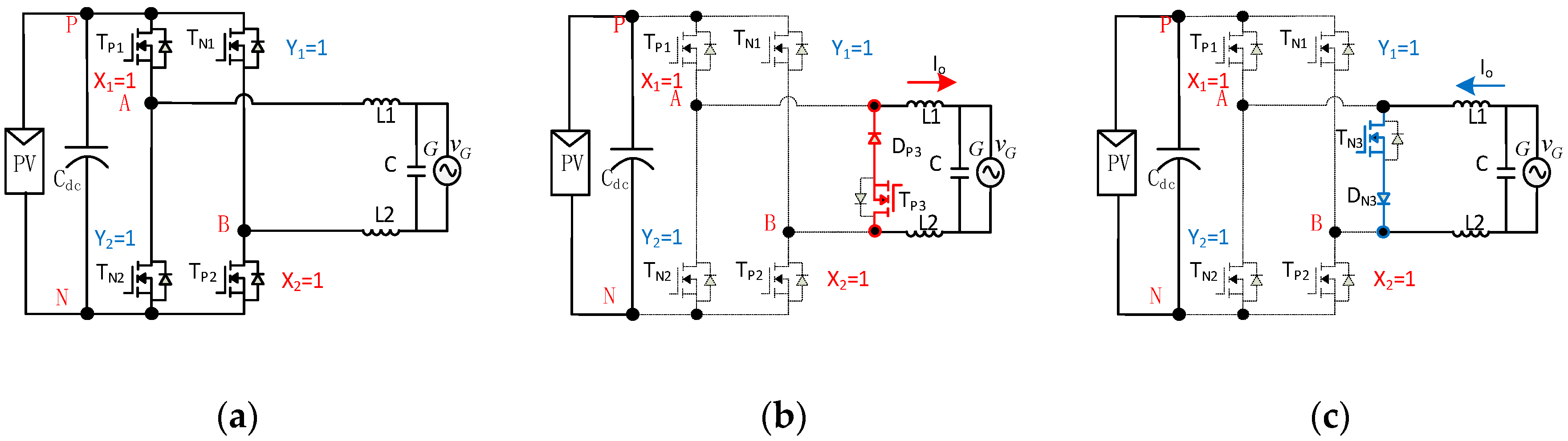
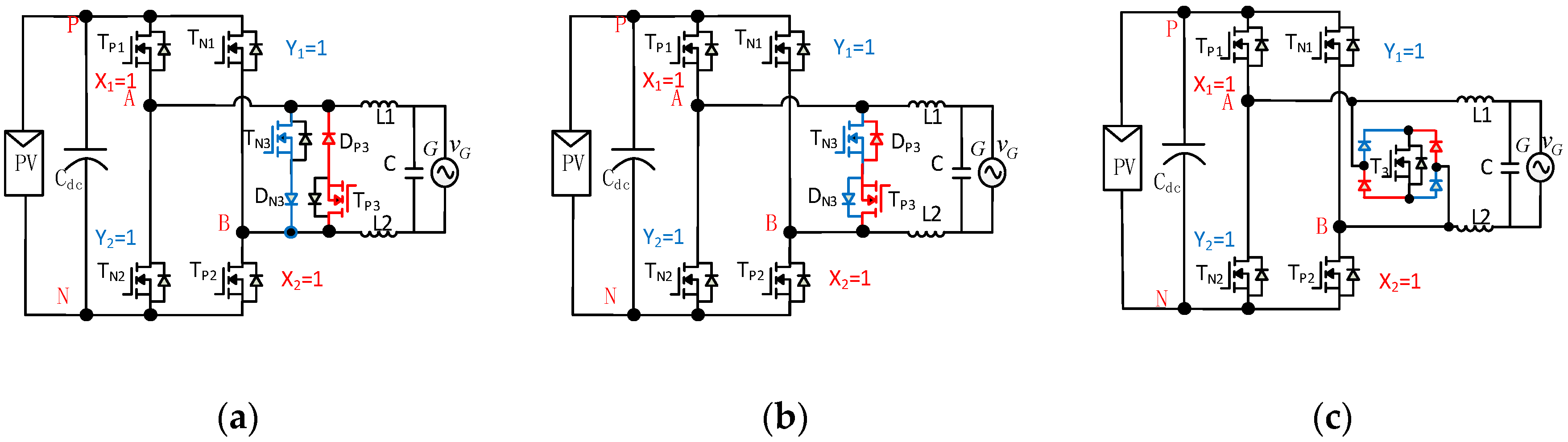
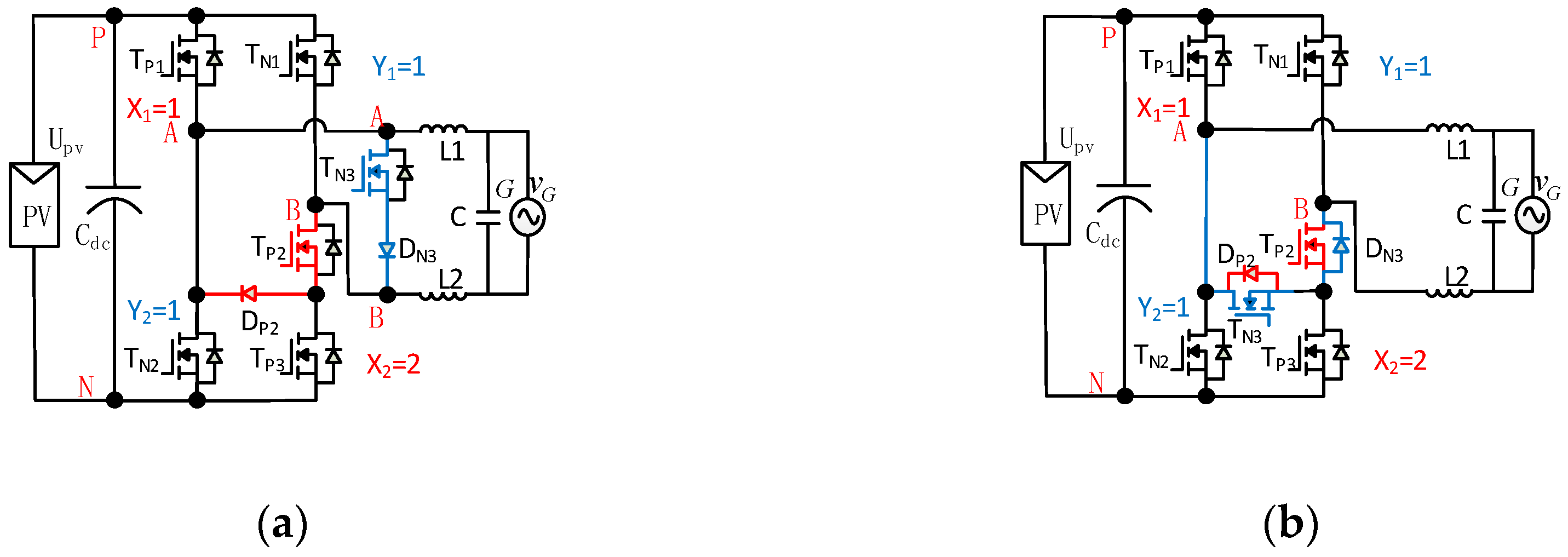
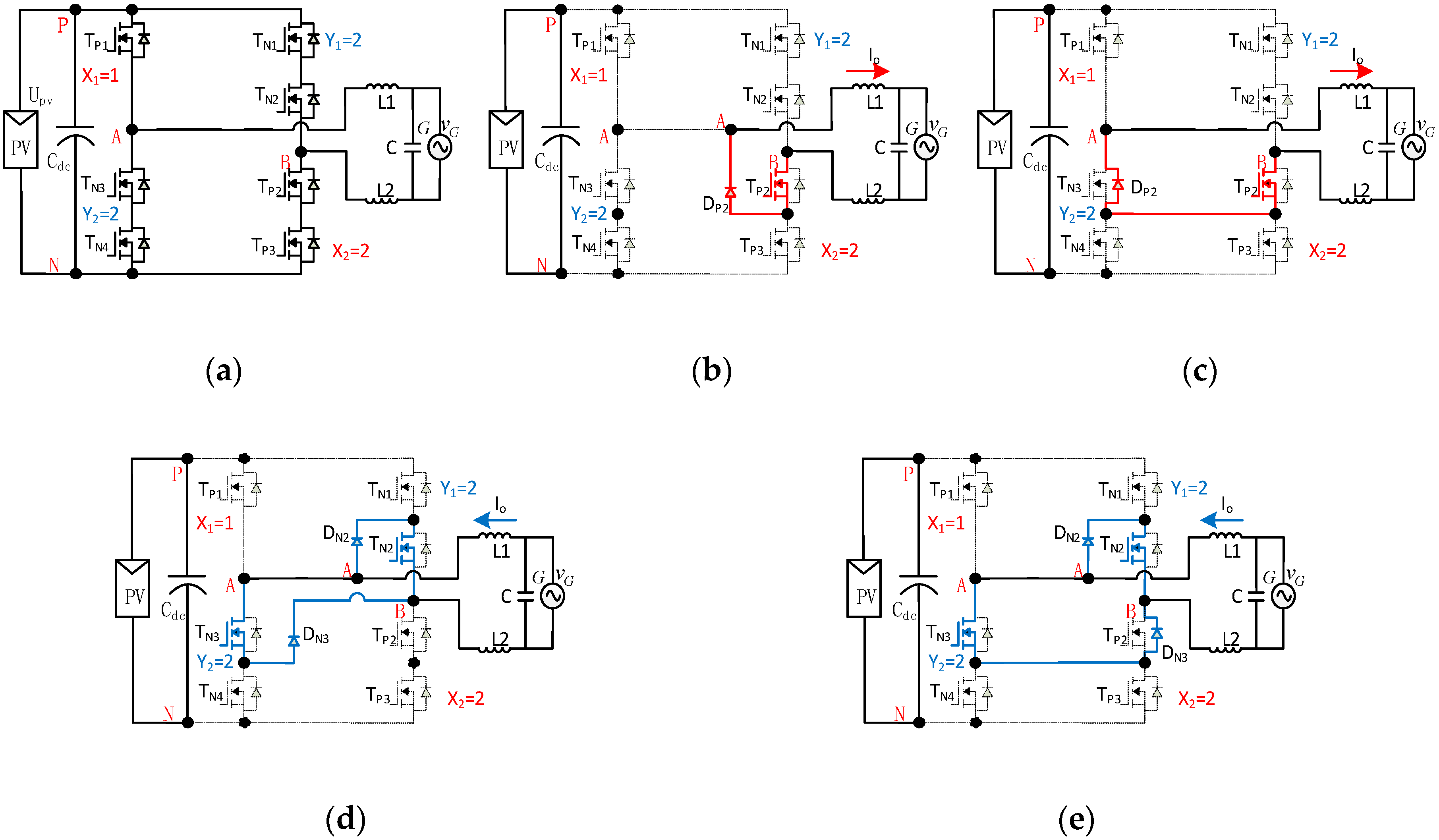
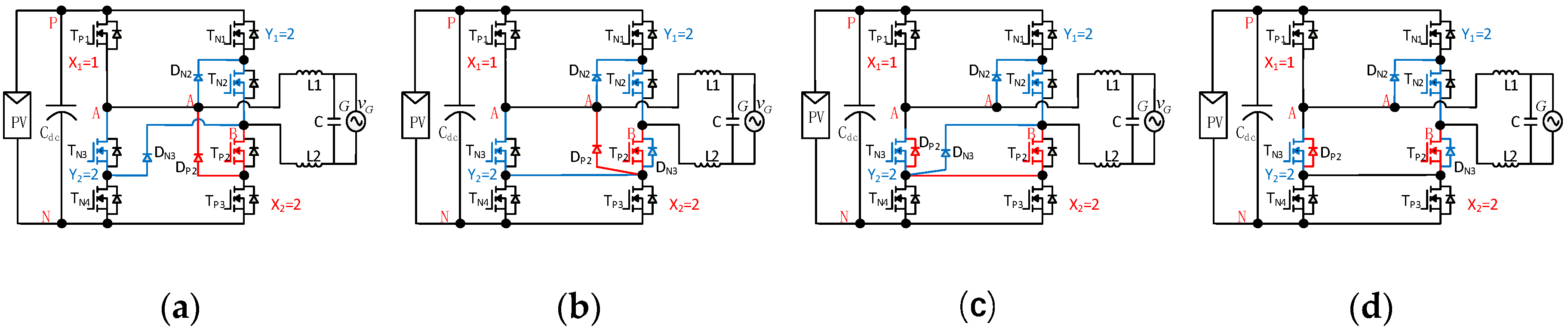
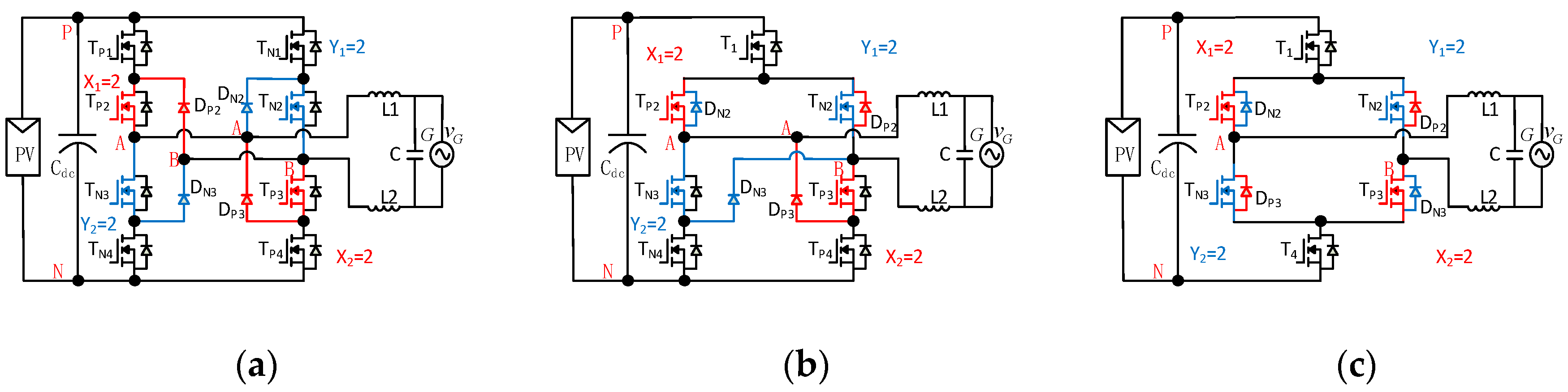
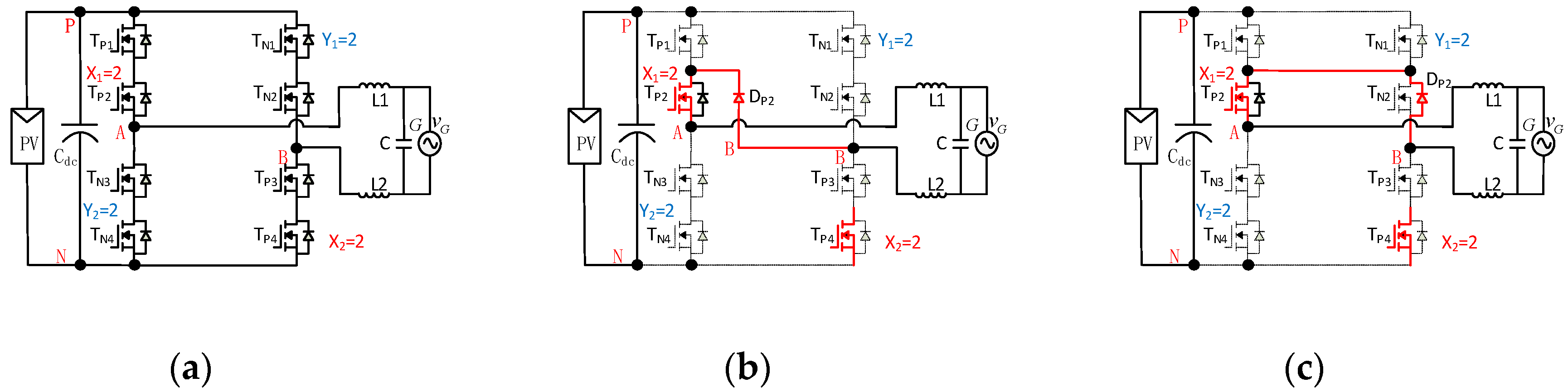
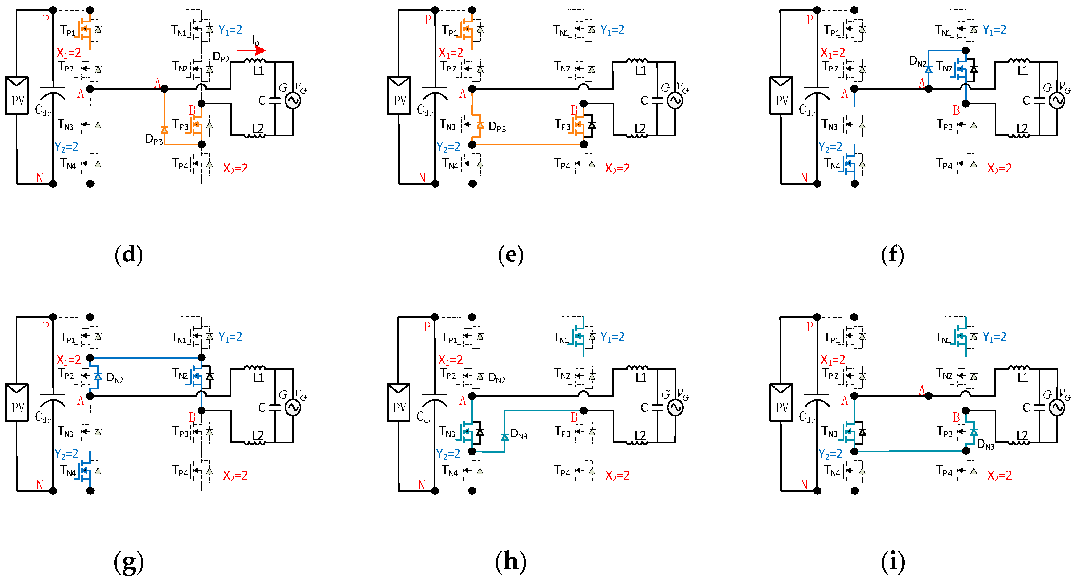
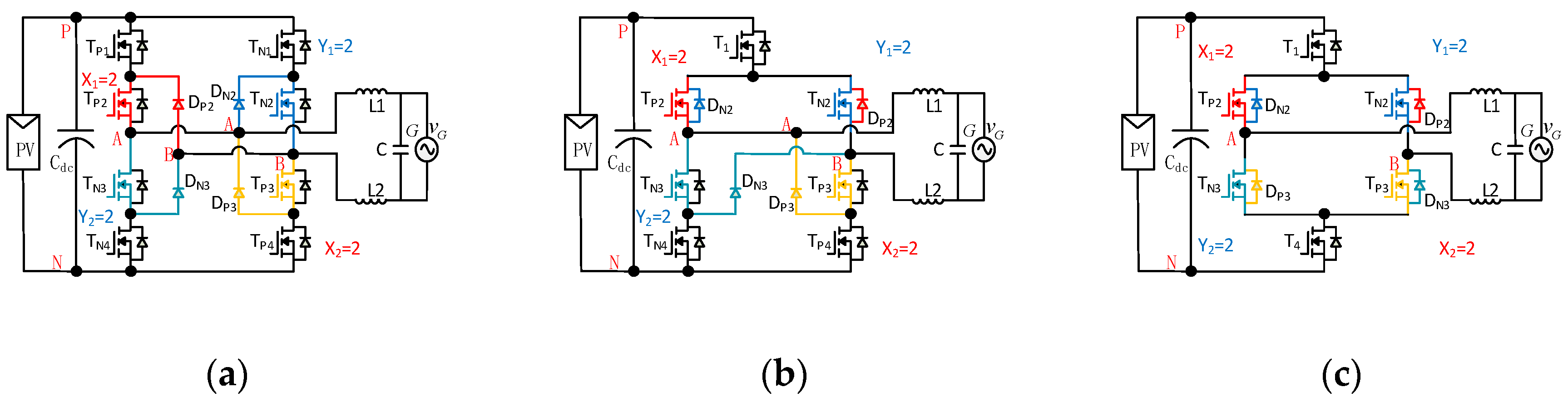
3.1. Case 1: M = 2 and N = 2

When M = 2 and N = 2, there is only one possibility to choose the combined values of X1, X2, Y1, and Y2, i.e., X1 = 1, X2 = 1, Y1 = 1, and Y2 = 1.
Figure 8 shows four modes derived from X1 = 1, X2 = 1, Y1 = 1 and Y2 = 1. The PC and NC modes are shown in Figure 8a. One switch, TP1, is adopted to connect points P and A due to X1 = 1; meanwhile, another switch, TP2, is viewed as a connection between points B and N on X2 = 1 at PC mode. Similarly, two other switches, TN1 and TN2, are added in NC mode with Y1 = 1 and Y2 = 1. Figure 8b shows PF mode. According to rule #1, four switches, i.e., TP1, TP2, TN1, and TN2, are off in PF mode. There is no available switch for output current flow. Thus, an extra switch, TP3, and an extra diode, Dp3, are added in series. This is the only choice available for PF mode. Similarly, for NF mode, an extra switch, TN3, and an extra diode, DN3, are added in series for output current flow, as shown in Figure 8c.
Three topologies derived from X1 = 1, X2 = 1, Y1 = 1, and Y2 = 1 are shown in Figure 9. Figure 9a can be achieved from Figure 8b,c in PF and NF modes. In Figure 9b, the body-diodes of switches TP3 and TN3 are used to replace the extra diodes in Figure 9a. Figure 9c is another topology in which four diodes plus one switch are used to replace the two switches, TP3 and TN3. These are well-known HERIC topologies [13,30].
The topologies from the MN principle may be divided into two families. Those in the first family have extra diode for output current flow in PF and NF modes. In contrast, the topologies in the second family don’t use the extra diode, and the body-diode of the switch is used to allow current to flow, as in the case in Figure 9b in PF and NF modes. Thus, two corresponding topological families under M = 2 and N = 2 are shown in Table 1.

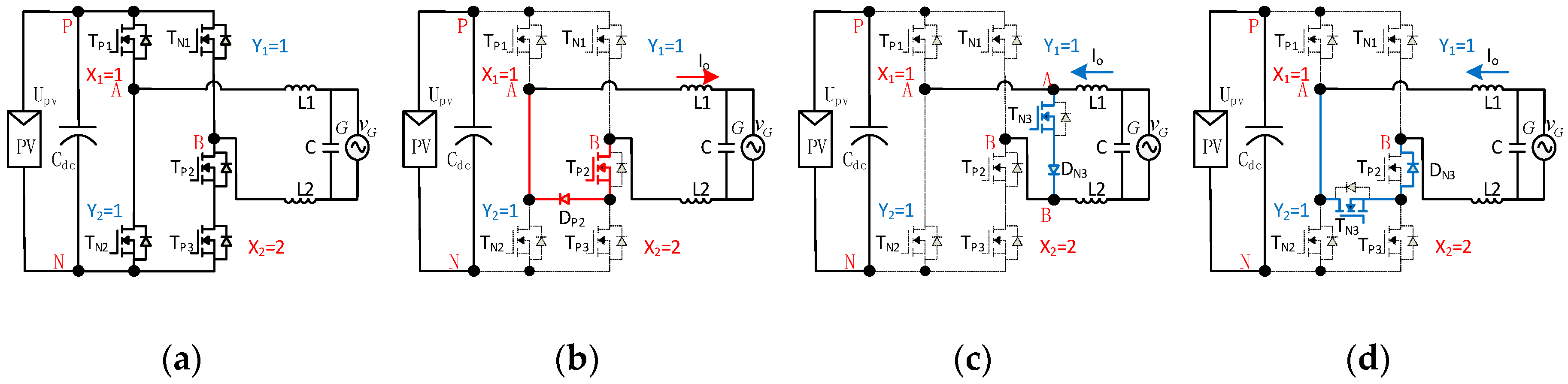
3.2. Case 2: M = 3 and N = 2 or M = 2 and N = 3

For M = 3, N = 2 or M = 2, N = 3, there are same topologies between M = 3, N = 2 and M = 2, N = 3, as they are equivalent by exchanging the two bridges. Thus, M = 3 and N = 2 is made as an example to explain the derivation method. M = 3 and N = 2 means there are two possibilities to choose the combined values of X1, X2, Y1, and Y2, i.e., X1 = 1, X2 = 2, Y1 = 1, and Y2 = 1, and X1 = 2, X2 = 1, Y1 = 1, and Y2 = 1. Considering the symmetrical characteristics with respect to terminals P and N, the two cases are the same. For the sake of brevity, only the former case is analyzed below.
Figure 10 shows four modes under X1 = 1, X2 = 2, Y1 = 1, and Y2 = 1. The PC and NC modes are shown in Figure 10a. One switch, TP1, is used to connect points P and A due to X1 = 1; meanwhile, switches TP2 and TP3 are viewed as a connection between point B and point N as X2 = 2 in PC mode. Similarly, two switches, TN1 and TN2, are added in NC mode with Y1 = 1 and Y2 = 1. According to rule #1, switches TP1, TP3, TN1, and TN2 are off in PF and NF modes. Switch Tp2 is on according to rule #3, and one diode Dp2 is added based on rule #2 in PF mode, as shown in Figure 10b. In NF mode, an extra switch, TN3, plus the diode DN3 are added in series to flow negative output current. The diode is added or served by the body diode of switch TP2. Thus, there are two circuits to realize NF mode, as shown in Figure 10c,d.
According to Figure 10, there are one circuit in PF mode and two circuits in NF mode. There are only two possibilities to combine PF and NF modes. Correspondingly, the two topologies derived from X1 = 1, X2 = 2, Y1 = 1, and Y2 = 1 are shown in Figure 11. Figure 11a shows the topology which combines the PF mode in Figure 10b and the NF mode in Figure 10c, while Figure 11b shows the topology which combines the PF mode in Figure 10b and the NF mode in Figure 10d. Two topological families under M = 3, N = 2 or M = 2, N = 3 are shown in Table 2.

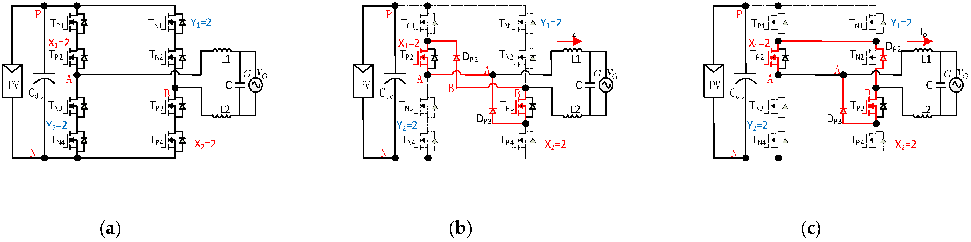
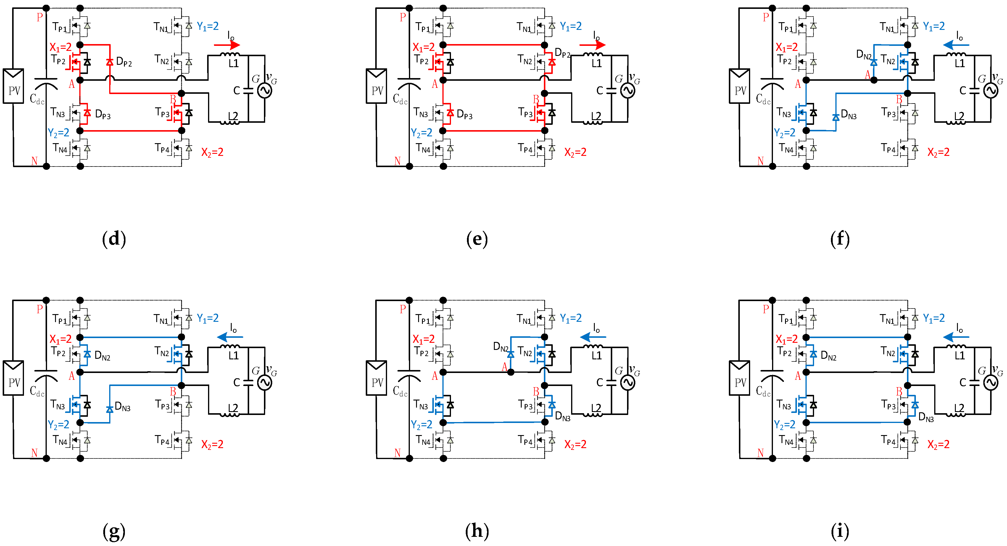
3.3. Case 3: M = 3 and N = 3

M = 3, which means there are two possibilities to choose the combined values of X1 and X2: X1 = 1, X2 = 2, and X1 = 2, X2 = 1. Similarly, N = 3 yields two possibilities to combine Y1 and Y2. One is Y1 = 1 and Y2 = 2 and the other is Y1 = 2 and X2 = 1. It should be noted that the same topologies exist between X1 = 2, X2 = 1, Y1 = 1, Y2 = 2, and X1 = 1, X2 = 2, Y1 = 2, Y2 = 1 when two bridges are exchanged. Thus, there are three possibilities: (1) X1 = 2, X2 = 1, Y1 = 2, and Y2 = 1; (2) X1 = 2, X2 = 1, Y1 = 1, and Y2 = 2; and (3) X1 = 1, X2 = 2, Y1 = 1, and Y2 = 2. Considering the symmetry between terminals P and N, case (1) is the same as case (3). For the sake of brevity, only cases (1) and (2) are analyzed below.
Figure 12 shows four modes under X1 = 2, X2 = 1, Y1 = 2, and Y2 = 1. The PC and NC modes are shown in Figure 12a. As shown in Figure 12a, six switches (TP1, TP2, TP3, TN1, TN2, and TN3) are used for X1 = 2, X2 = 1, Y1 = 2, and Y2 = 1. According to rule #1, switches TP1, TP3, TN1, and TN3 are off in PF and NF modes. One rest switch, TP2, is on according to rule #3, and one diode, DP2, is added based on rule #2 in PF mode, as shown in Figure 12b. Diode DP2 can also be served by the body-diode of switch TN2. The reflected PF mode is shown in Figure 12c. For NF mode, switch TN2 is on for negative output current flow. An extra diode, DN2, is added, as shown in Figure 12d. The body-diode of switch TP2 is served as the diode DN2, as shown in Figure 12e.
According to Figure 12, there are two circuits in PF mode and two in NF mode. There are four possibilities to combine PF and NF modes. Correspondingly, four topologies derived from X1 = 2, X2 = 1, Y1 = 2, and Y2 = 1 are shown in Figure 13. Figure 13a shows the topology combining the PF mode in Figure 12b and the NF mode in Figure 12d. Figure 13b shows the topology combining the PF mode in Figure 12b and the NF mode in Figure 12e. Figure 13c shows the topology combining the PF mode in Figure 12c and the NF mode in Figure 12d, and Figure 13d shows the topology combining the PF mode in Figure 12c and the NF mode in Figure 12e.
According to rule #4, the extra diode DP2 can be absent due to the presence of the body-diode of switch TN2 in Figure 13b. Similarly, the extra diode DN2 can be absent owing to the presence of the body-diode of switch TP2 in Figure 13c. In Figure 13b–d, the two switches, TP1 and TN1, are combined into one switch T1. Thus, the topologies in Figure 13b–d are the same.
Similarly, one topology derived from X1 = 2, X2 = 1, Y1 = 1, and Y2 = 2 is shown in Figure 14.
Correspondingly, two topological families under M = 3 and N = 3 are shown in Table 3.

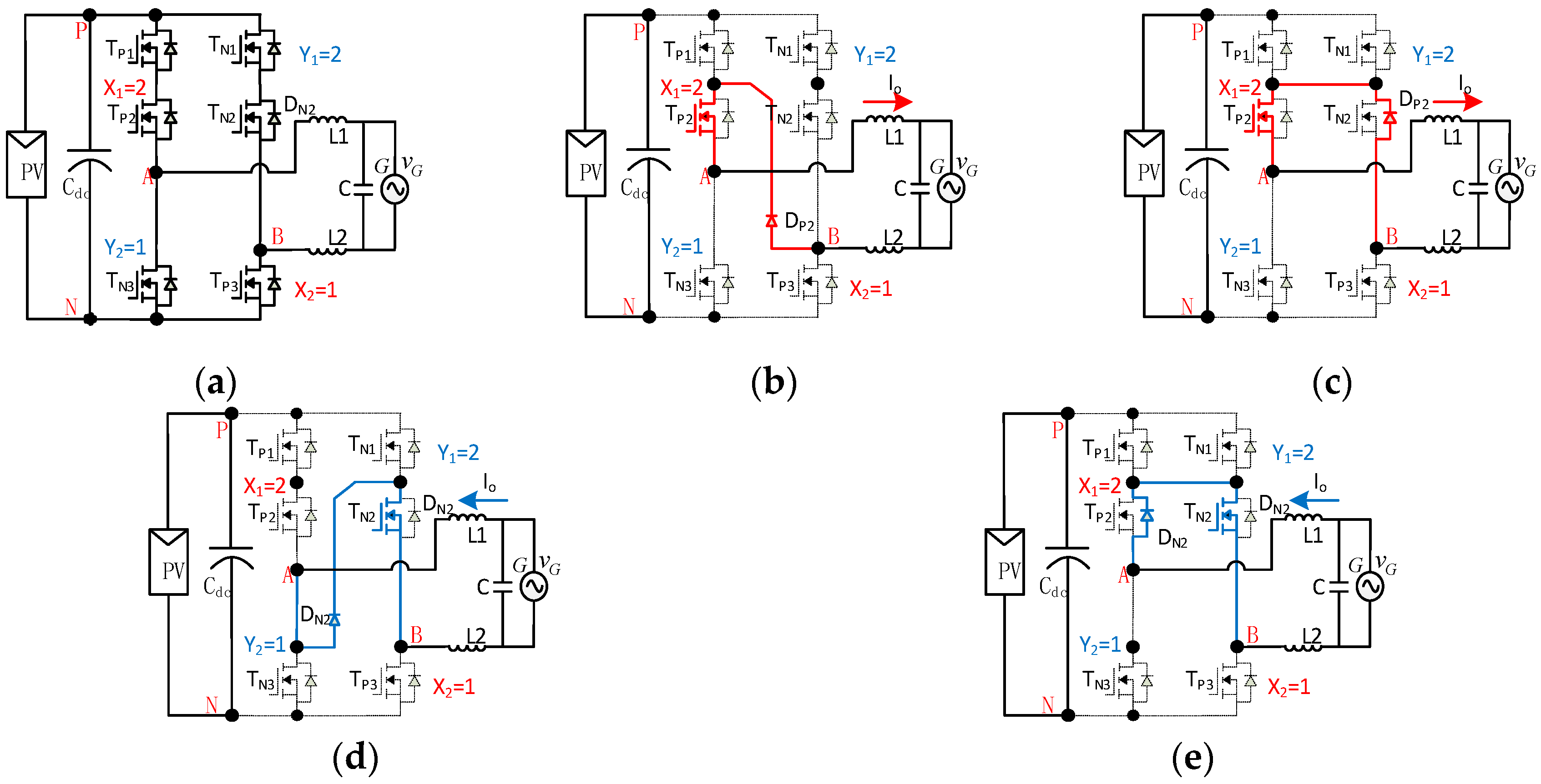
3.4. Case 4: M = 3 and N = 4 or M = 4 and N = 3

The same topologies exist between M = 3, N = 4 and M = 4, N = 3, as they are equivalent by exchanging the two bridges. For M = 3 and N = 4, M = 3 means that there are two possibilities to choose the combined values of X1 and X2: one is X1 = 2 and X2 = 1, and the other is X1 = 1 and X2 = 2. Similarly, N = 4 means three possibilities to combine Y1 and Y2. However, only one combination is available according to Equation (9), i.e., Y1 = 2 and Y2 = 2.
Thus, there are two possibilities to choose the combined values of X1, X2, Y1, and Y2: one is X1 = 1, X2 = 2, Y1 = 2, and Y2 = 2, and the other is X1 = 2, X2 = 1, Y1 = 2, and Y2 = 2. Considering the symmetry between terminals P and N, the two cases are the same. Figure 15 shows four modes under X1 = 1, X2 = 2, Y1 = 2, and Y2 = 2.
The PC and NC modes are shown in Figure 15a. Seven switches (TP1, TP2, TP3, TN1, TN2, TN3, and TN4) are used for X1 = 1, X2 = 2, Y1 = 2, and Y2 = 2, as shown in Figure 15a. From rule #1, the switches TP1, TP3, TN1, and TN4 are off in PF and NF modes. Switch TP2 is on according to rule #3, and one diode DP2 is added based on rule #2 in PF mode, as shown in Figure 15b. Diode DP2 is served by the body-diode of switch TN3; the reflected PF mode is shown in Figure 15c. For NF mode, two switches, i.e., TN2 and TN3, are on for negative output current flow according to rule #3, and two extra diodes, DN2 and DN3, are added from rule #2, as shown in Figure 15d. The body-diode of switch TP2 serves as the diode DN3, as shown in Figure 15e.
According to the above analysis, there are two circuits in PF mode and two in NF mode. Thus, four possible topologies are shown in Figure 16. Figure 16a shows the topology combining the PF mode in Figure 15b and the NF mode in Figure 15d. The other three topologies are shown in Figure 16b–d, respectively; however, they are the same, as diode DP2 in Figure 16b and diode DN3 in Figure 16c can be absent from rule #4. Furthermore, two switches, i.e., TP3 and TN4, are merged into one switch, i.e., T4.
Correspondingly, two topological families under M = 3 and N = 4 or M = 4 and N = 3 are shown in Table 4.

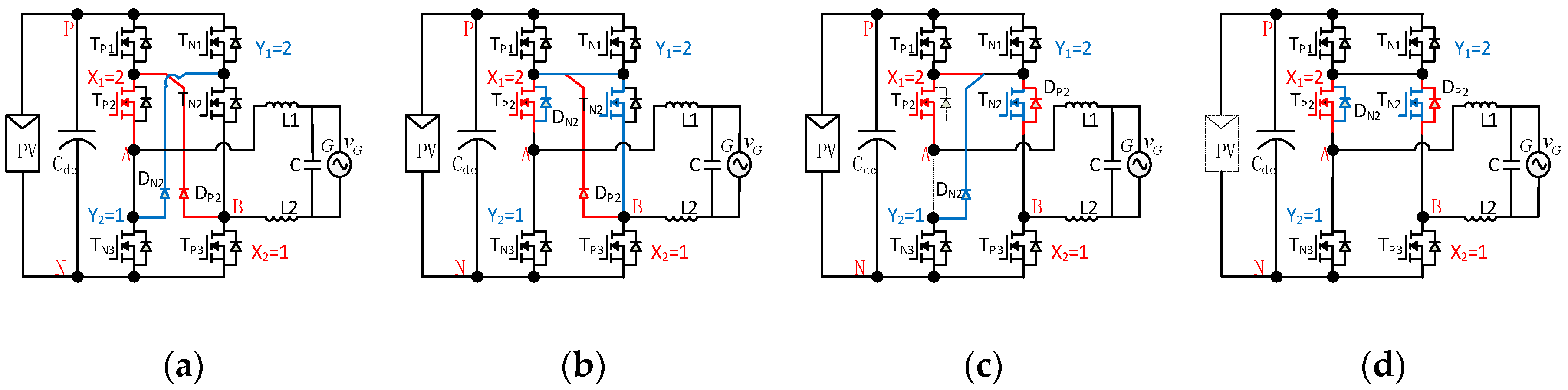
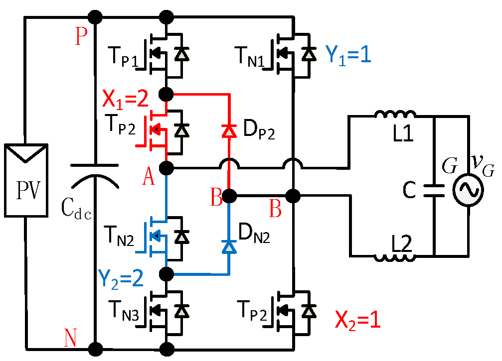
3.5. Case 5: M = 4 and N = 4

In this case, M = 4 and N = 4. According to Equation (9), M = 4 and N = 4 means only one available possibility to choose the combined values of X1, X2, Y1, and Y2, i.e., X1 = 2, X2 = 2, Y1 = 2, and Y2 = 2.
Figure 17 shows four modes under X1 = 2, X2 = 2, Y1 = 2, and Y2 = 2. As shown in Figure 17a, eight switches (TP1~TP4 and TN1~TN4) are used for X1 = 2, X2 = 2, Y1 = 2, and Y2 = 2 in PC and NC modes. With the reference of the above analysis of Cases 1~4, it is easy to make a similar analysis. For the sake of brevity, this is included here.
It may be observed from Figure 17 that there are four circuits in PF mode and four in NF mode. Thus, sixteen possible topologies may be derived from the MN principle. However, these topologies can be simplified based on rule #4, and the four topologies derived from X1 = 2, X2 = 2, Y1 = 2, and Y2 = 2 are shown in Figure 18.
Two corresponding topological families under M = 4 and N = 4 are shown in Table 5.

3.6. All Simplfied Topologies from MN Principle

From the above analysis, two corresponding topological families are summarized in Table 6.
It may be observed from the above analysis that the MN principle can be used to derive all the possible topologies for a single-phase, full bridge, transformerless inverter. Furthermore, thirteen simplified topologies from the MN principle are provided in this paper. All existing topologies (R1–R8, R13) have been covered, and five new topologies marked from R9 to R12 have been found.
For the two topological families with the same M and N, the topologies without an extra diode are of lower cost than those with the extra diode, as the body-diode of switch in the former is used to replace the extra diode; however, the efficiency of the former will likely be a little lower, as that diode has better performance than the body-diode.
(M + N) is the number of conduction switches in PC and NC modes; the bigger (M + N), the higher the conduction loss. Thus, M = N = 2 is the best choice in terms of low conduction loss.
Although M = 4 and N = 4 means large conduction loss under USPWM, the topologies from M = 4 and N = 4 can also work in DFSPWM, where the equivalent switching frequency is double, and the size of the low pass filter is reduced. A detailed description about DFUSWPM will be given in the next section.

4. Topology Derivation under DFUSPWM

In this section, topology derivation methodology is introduced under DFUSPWM. The unified topology model and MN principle are extended to the topologies under DFUSPWM.

4.1. Principle of DFUSPWM

The principle of DFUSPWM is shown in Figure 19. Differential-mode voltage VAB is a three-level waveform.
The levels are +VPN, 0, and −VPN. There are six modes in total line-frequency period. The inverter is working in positive conduction (PC) mode and negative conduction (NC) mode when VAB equals +VPN and −VPN, respectively. There are four modes if VAB equals 0.
To achieve double frequency of voltage VAB, there are two interleaved freewheeling modes when the grid voltage is positive: one is used to refer to the freewheeling current flowing through top switch, which is defined as PFT mode. The other one, called “PFB mode” is used to flow freewheeling current through bottom switch. Similarly, two interleaved freewheeling modes, called “NFT mode” and “NFB mode”, are used in NF mode. The freewheeling current flows through the top switch in NFT and through the bottom switch in NFB mode.
The modes rotate in the sequence of PFT, PC, PFB, and PC in the positive half cycle of the grid voltage. Similarly, the modes rotate in the sequence of NFT, NC, NFB, and NC in the negative half cycle. Thus, the frequency of output voltage VAB is double the switch frequency.
The six modes based on H4 topology in DFUSPWM are shown in Figure 20. The PC and NC modes are shown in Figure 20a and Figure 20b, respectively. In the positive half cycle of grid voltage, two PF modes, i.e., PFT and PFB, are shown in Figure 20c,d. Similarly, two NF modes, i.e., NFT and NFB, are shown in Figure 20e,f in the negative half cycle of the grid voltage.

4.2. Unified Topology Model of DFUSPWM

Figure 21 shows six modes from the unified topology model under DFUSPWM.
All rules under USPWM mentioned in Section 2 are also suitable for DFUSPWM. According to rule #1, points A and B must be disconnected from points P and N in the four freewheeling modes, i.e., the two PF modes and the two NF modes. From rule #2, the branch between points A and B is short-circuited for output current flow. Two new controlled branches, BCA ^ and BEA ^ , are added to flow the positive current in Figure 21c,d. Two controlled branches, ADB ^ and AFB ^ , are added to flow the negative current in Figure 21e,f.
For DFUSPWM, there are two PC modes in a switching period. Thus, according to rule #1, there are at least two couple switches to alternately turn on/off to achieve double frequency. For example, there are two switches, i.e., TP1 connected to point P and TP2 connected to point A, between point P and point A, and two, i.e., TP3 connected to point B and TP4 connected to point N, between point B and point N. Switches TP1 and TP2 are connected in series, as are TP3 and TP4. Switches TP1 and TP3 turn on/off at the same time, and TP2 and TP4 are kept on or off at the same time. Thus, there are two possibilities to disconnect points P and A, and points B and N: one is that switches TP1 and TP3 turn off. The other is that switches TP2 and TP4 turn off. Once switches TP1 and TP3 turn off in PFT mode, switch TP2 is kept on and can be used to construct a freewheeling branch because it connects to point A. Similarly, switch TP3 is kept on and serves to construct a freewheeling branch in the PFB mode when switches TP2 and TP4 turn off. Thus, two PF modes can be achieved when X1 = 2 and X2 = 2. The same is true with Y1 = 2, Y2 = 2.
Figure 22 shows six modes under X1 = 2, X2 = 2, Y1 = 2, and Y2 = 2. The PC and NC modes are shown in Figure 22a. Eight switches (TP1~TP4 and TN1~TN4) are used. The same driving signals are provided for couples of switches TP1 and TP3, TP2 and TP4, TN1 and TN3, and TN2 and TN4.
In PFT mode, switches TP1, TP3, TN1, TN2, TN3, and TN4 are off, and switches TP2 and TP4 are on. One diode, DP2, is added for the positive output current flow, as shown in Figure 22b. Diode DP2 is served by the body-diode of switch TN2. The reflected PFT mode is shown in Figure 22c.
In PFB mode, switches TP2, TP4, TN1, TN2, TN3, and TN4 are off, and switches TP1 and TP3 are on. One diode, DP3, is added for positive output current flow, as shown in Figure 22d. Diode DP3 is served by the body-diode of switch TN3, as shown in Figure 22e. It is easy to make a similar analysis for NFT and NFB modes. Figure 22f,g show the two NFT modes, while the two NFB modes are shown in Figure 22h,i.
It should be noted from the above analysis that there are two PFT modes, two PFB modes, two NFT modes, and two NFB modes. There are eight possible topologies through choosing one PFT mode, one PFB mode, one NFT mode, and one NFB mode. According to rule #4, the four typical topologies in Figure 23 are derived from the MN principle.
Two corresponding topological families under DFUSPWM are shown in Table 7.

5. Conclusions

In this paper, a topology derivation methodology under USPWM is proposed to determine all possible full-bridge topologies for small leakage current. A unified circuit model based on USPWM is provided. Secondly, a mathematic method called the “MN principle” is then proposed to determine all possible topologies. Four rules and a derivation procedure are also provided. Thirteen simplified topologies are derived using this method. All existing topologies have been covered, and four new topologies have been found. These topologies can be classified into two topology families: the first includes topologies in which extra diodes are used for current flowing, while the body-diode functions as the extra diode to flow freewheeling current in the second family topologies. Finally, the proposed method is extended to the topologies under DFUSPWM, and three corresponding topologies have been derived, and two new topologies found.

Author Contributions

Conceptualization, X.Y., X.W.; funding acquisition, X.W.; investigation, X.Y.; software, X.Z.; validation, X.Z., X.W.; writing—original draft, X.Y.; writing—review and editing, H.W. and Y.-F.L. All authors have read and agreed to the published version of the manuscript.

Funding

Research on Topology, Passive Current Sharing Mechanism and Control for Multiphase Resonant Converter with Coupled Resonant Tank: 51977069; Research on High-power and High-efficiency Electro-acoustic Transduction Mechanism and Control Method: 51837005.

Conflicts of Interest

The authors declare no conflicts of interest.

References

  1. Sun, K.; Zhang, L.; Xing, Y.; Guerrero, J.M. A Distributed Control Strategy Based on DC Bus Signaling for Modular Photovoltaic Generation Systems with Battery Energy Storage. IEEE Trans. Power Electron. 2011, 26, 3032–3045. [Google Scholar] [CrossRef] [Green Version]
  2. EPIA. Global Market Outlook for Photovoltaics 2013–2017; European Photovoltaic Industry Association: Brussels, Belgium, 2013. [Google Scholar]
  3. Kjaer, S.B.; Pedersen, J.K.; Blaabjerg, F. A review of single-phase grid-connected inverters for photovoltaic modules. IEEE Trans. Ind. Appl. 2005, 41, 1292–1306. [Google Scholar] [CrossRef]
  4. Blaabjerg, F.; Zhe, C.; Kjaer, S.B. Power electronics as efficient interface in dispersed power generation systems. IEEE Trans. Power Electron. 2004, 19, 1184–1194. [Google Scholar] [CrossRef]
  5. Quan, L.; Wolfs, P. A Review of the Single Phase Photovoltaic Module Integrated Converter Topologies with Three Different DC Link Configurations. IEEE Trans. Power Electron. 2008, 23, 1320–1333. [Google Scholar] [CrossRef] [Green Version]
  6. Power Generation Systems Connected to the Low-Voltage Distribution Network, VDE-AR-N 4105. Available online: https://www.sogou.com/link?url=hedJjaC291MdqKRdyYP6xaEfyF6gLPTmC2Ly98cd-IVBavtdX5bT4M0N-aB7Vy-zp32izvdhNQ_l-ZZN6CSHZQ (accessed on 1 August 2011).
  7. Standard for Inverters, Converters, Controllers, and Interconnection System Equipment for Use with Distributed Energy Resources. UL 1741. Available online: https://standardscatalog.ul.com/standards/en/standard_1741_2 (accessed on 28 January 2010).
  8. Automatic Disconnection Device between a Generator and the Public Low-Voltage Grid, DIN VDE V 0126-1-1. Available online: https://www.beuth.de/en/pre-standard/din-vde-v-0126-1-1/187485608 (accessed on 1 August 2013).
  9. Lopez, O.; Teodorescu, R.; Freijedo, F.; Doval-Gandoy, J. Eliminating ground current in a transformerless photovoltaic application. IEEE Trans. Energy Convers. 2010, 25, 140–147. [Google Scholar] [CrossRef]
  10. Gonzalez, R.; Gubia, E.; Lopez, J.; Marroyo, L. Transformerless Single-Phase Multilevel-Based Photovoltaic Inverter. IEEE Trans. Ind. Electron. 2008, 55, 2694–2702. [Google Scholar] [CrossRef]
  11. Xiao, H.; Xie, S. Transformerless Split-Inductor Neutral Point Clamped Three-Level PV Grid-Connected Inverter. IEEE Trans. Power Electron. 2012, 27, 1799–1808. [Google Scholar] [CrossRef]
  12. Victor, M.; Greizer, K.; Bremicker, A. Method of Converting a Direct Current Voltage from a Source of Direct Current Voltage, More Specifically from a Photovotatic Source of Direct Current Voltage, into a Alternating Current Voltage. U.S. Patent 7,411,802, 12 August 2008. [Google Scholar]
  13. Schmidt, H.; Siedle, C.; Ketterer, J. Wechselrichter zum Unwandeln einer Elektrischen Gleichspannung in einen Wechselstrom oder eine Wechselspannung. EP Patent 2 086 102 A2, 15 May 2003. [Google Scholar]
  14. Patino, D.G.; Erira, E.G.; Fuelagan, J.R.; Rosero, E.E. Implementation a HERIC inverter prototype connected to the grid controlled by SOGI-FLL. In Proceedings of the 2015 IEEE Workshop on Power Electronics and Power Quality Applications (PEPQA), Bogota, Colombia, 2–4 June 2015; pp. 1–6. [Google Scholar]
  15. Zhang, L.; Sun, K.; Xing, Y.; Xing, M. H6 Transformerless Full-Bridge PV Grid-Tied Inverters. IEEE Trans. Power Electron. 2014, 29, 1229–1238. [Google Scholar] [CrossRef]
  16. Yu, W.; Lai, J.S.; Qian, H.; Hutchens, C.; Zhang, J.; Lisi, G.; Djabbari, A.; Smith, G.; Hegarty, T. High-efficiency inverter with H6-type configuration for photovoltaic non-isolated ac module applications. In Proceedings of the 2010 Twenty-Fifth Annual IEEE Applied Power Electronics Conference and Exposition (APEC), Palm Springs, CA, USA, 21–25 February 2010; pp. 1056–1061. [Google Scholar]
  17. Yang, B.; Li, W.; Gu, Y.; Cui, W.; He, X. Improved Transformerless Inverter with Common-Mode Leakage Current Elimination for a Photovoltaic Grid-Connected Power System. IEEE Trans. Power Electron. 2012, 27, 752–762. [Google Scholar] [CrossRef]
  18. Su, X.; Sun, Y.; Lin, Y. Analysis on Leakage Current in Transformerless Single-Phase PV Inverters Connected to the Grid. In Proceedings of the Power and Energy Engineering Conference (APPEEC), 2011 Asia-Pacific, Wuhan, China, 25–28 March 2011; pp. 1–5. [Google Scholar]
  19. Xiao, H.F.; Ke, L.; Li, Z. A Quasi-Unipolar SPWM Full-Bridge Transformerless PV Grid-Connected Inverter with Constant Common-Mode Voltage. IEEE Trans. Power Electron. 2015, 30, 3122–3132. [Google Scholar] [CrossRef]
  20. Xiao, H.; Xie, S.; Chen, Y.; Huang, R. An Optimized Transformerless Photovoltaic Grid-Connected Inverter. IEEE Trans. Ind. Electron. 2011, 58, 1887–1895. [Google Scholar] [CrossRef]
  21. Wang, J.; Ji, B.; Zhao, J.; Yu, J. From H4, H5 to H6 Standardization of full-bridge single phase photovoltaic inverter topologies without ground leakage current issue. In Proceedings of the 2012 IEEE Energy Conversion Congress and Exposition (ECCE), Raleigh, NC, USA, 15–20 September 2012; pp. 2419–2425. [Google Scholar]
  22. Vazquez, G.; Martinez-Rodriguez, P.R.; Sosa, J.M.; Escobar, G.; Juarez, M.A. Transformerless single-phase multilevel inverter for grid tied photovoltaic systems. In Proceedings of the Industrial Electronics Society, IECON 2014—40th Annual Conference of the IEEE, Dallas, TX, USA, 29 October–1 November 2014; pp. 1868–1874. [Google Scholar]
  23. Vazquez, G.; Martinez-Rodriguez, P.R.; Sosa, J.M.; Escobar, G.; Arau, J. A modulation strategy for single-phase HB-CMI to reduce leakage ground current in transformer-less PV applications. In Proceedings of the Industrial Electronics Society, IECON 2013—39th Annual Conference of the IEEE, Vienna, Austria, 10–13 November 2013; pp. 210–215. [Google Scholar]
  24. Figueredo, R.S.; de Carvalho, K.C.M.; Ama, N.R.N.; Junior, L.M. Leakage current minimization techniques for single-phase transformerless grid-connected PV inverters—An overview. In Proceedings of the Power Electronics Conference (COBEP), Gramado, Brazil, 27–31 October 2013; pp. 517–524. [Google Scholar]
  25. Hu, S.; Cui, W.; Li, W.; He, X.; Cao, F. A high-efficiency single-phase inverter for transformerless photovoltaic grid-connection. In Proceedings of the Energy Conversion Congress and Exposition (ECCE), Pittsburgh, PA, USA, 14–18 September 2014; pp. 4232–4236. [Google Scholar]
  26. Salmon, J.; Knight, A.; Ewanchuk, J. Single phase multi-level PWM Inverter topologies using coupled inductors. In Proceedings of the Power Electronics Specialists Conference, Rhodes, Greece, 15–19 June 2008; pp. 802–808. [Google Scholar]
  27. Ozkan, Z.; Hava, A.M. Leakage current analysis of grid connected transformerless solar inverters with zero vector isolation. In Proceedings of the Energy Conversion Congress and Exposition (ECCE), Phoenix, AZ, USA, 17–22 September 2011; pp. 2460–2466. [Google Scholar]
  28. Lopez, O.; Teodorescu, R.; Freijedo, F.; DovalGandoy, J. Leakage current evaluation of a singlephase transformerless PV inverter connected to the grid. In Proceedings of the Applied Power Electronics Conference, APEC 2007—Twenty Second Annual IEEE, Anaheim, CA, USA, 25 February–1 March 2007; pp. 907–912. [Google Scholar]
  29. Ma, L.; Tang, F.; Zhou, F.; Jin, X.; Tong, Y. Leakage current analysis of a single-phase transformer-less PV inverter connected to the grid. In Proceedings of the 2008 IEEE International Conference on Sustainable Energy Technologies, Singapore, 24–27 November 2008; pp. 285–289. [Google Scholar]
  30. Kerekes, T.; Teodorescu, R.; Rodriguez, P.; Vazquez, G.; Aldabas, E. A New High-Efficiency Single-Phase Transformerless PV Inverter Topology. IEEE Trans. Ind. Electron. 2011, 58, 184–191. [Google Scholar] [CrossRef] [Green Version]
  31. Ji, B.; Wang, J.; Zhao, J. High-Efficiency Single-Phase Transformerless PV H6 Inverter with Hybrid Modulation Method. IEEE Trans. Ind. Electron. 2013, 60, 2104–2115. [Google Scholar] [CrossRef]
  32. Islam, M.; Mekhilef, S. A new high efficient transformerless inverter for single phase grid-tied photovoltaic system with reactive power control. In Proceedings of the Applied Power Electronics Conference and Exposition (APEC), Charlotte, NC, USA, 15–19 March 2015; pp. 1666–1671. [Google Scholar]
  33. Islam, M.; Mekhilef, S. High efficiency transformerless MOSFET inverter for grid-tied photovoltaic system. In Proceedings of the 2014 Twenty-Ninth Annual IEEE Applied Power Electronics Conference and Exposition (APEC), Fort Worth, TX, USA, 16–20 March 2014; pp. 3356–3361. [Google Scholar]
  34. San, G.; Qi, H.; Wu, J.; Guo, X. A new three-level six-switch topology for transformerless photovoltaic systems. In Proceedings of the 2012 7th International Power Electronics and Motion Control Conference (IPEMC), Harbin, China, 2–5 June 2012; pp. 163–166. [Google Scholar]
  35. Freddy, T.K.S.; Rahim, N.A.; Wooi-Ping, H.; Seng, C.H. Comparison and Analysis of Single-Phase Transformerless Grid-Connected PV Inverters. IEEE Trans. Power Electron. 2014, 29, 5358–5369. [Google Scholar] [CrossRef]
  36. Yu, W.; Lai, J.S.; Qian, H.; Hutchens, C.; Zhang, J.; Lisi, G.; Djabbari, A.; Smith, G.; Hegarty, T. A novel H6 topology and Its modulation strategy for transformerless photovoltaic grid-connected inverters. In Proceedings of the 2014 16th European Conference on Power Electronics and Applications (EPE’14-ECCE Europe), Lappeenranta, Finland, 26–28 August 2014; pp. 1–8. [Google Scholar]
  37. Dong, D.; Luo, F.; Boroyevich, D.; Mattavelli, P. Leakage Current Reduction in a Single-Phase Bidirectional AC-DC Full-Bridge Inverter. IEEE Trans. Power Electron. 2012, 27, 4281–4291. [Google Scholar] [CrossRef]
  38. Cui, W.; Yang, B.; Zhao, Y.; Li, W.; He, X. A novel single-phase transformerless grid-connected inverter. In Proceedings of the IECON 2011—37th Annual Conference on IEEE Industrial Electronics Society, Melbourne, Australia, 7–10 November 2011; pp. 1126–1130. [Google Scholar]
  39. Gu, B.; Dominic, J.; Lai, J.-S.; Chen, C.-L.; LaBella, T.; Chen, B. High Reliability and Efficiency Single-Phase Transformerless Inverter for Grid-Connected Photovoltaic Systems. IEEE Trans. Power Electron. 2013, 28, 2235–2245. [Google Scholar] [CrossRef]
  40. Gu, B.; Dominic, J.; Chen, B.; Lai, J.-S. A high-efficiency single-phase bidirectional AC-DC converter with miniminized common mode voltages for battery energy storage systems. In Proceedings of the Energy Conversion Congress and Exposition (ECCE), Denver, CO, USA, 15–19 September 2013; pp. 5145–5149. [Google Scholar]
  41. Basu, K.; Mohan, N. A High-Frequency Link Single-Stage PWM Inverter with Common-Mode Voltage Suppression and Source-Based Commutation of Leakage Energy. IEEE Trans. Power Electron. 2014, 29, 3907–3918. [Google Scholar] [CrossRef]
  42. Barater, D.; Buticchi, G.; Crinto, A.S.; Franceschini, G.; Lorenzani, E. Unipolar PWM Strategy for Transformerless PV Grid-Connected Converters. IEEE Trans. Energy Convers. 2012, 27, 835–843. [Google Scholar] [CrossRef]
  43. Barater, D.; Buticchi, G.; Crinto, A.S.; Franceschini, G.; Lorenzani, E. A new proposal for ground leakage current reduction in transformerless grid-connected converters for photovoltaic plants. In Proceedings of the 35th Annual Conference of IEEE Industrial Electronics, 2009, IECON ’09, Porto, Portugal, 3–5 November 2009; pp. 4531–4536. [Google Scholar]
  44. Anandababu, C.; Fernandes, B.G. Improved full-bridge neutral point clamped transformerless inverter for photovoltaic grid-connected system. In Proceedings of the 39th Annual Conference of the IEEE Industrial Electronics Society, IECON 2013, Vienna, Austria, 10–13 November 2013; pp. 7996–8001. [Google Scholar]
  45. Anandababu, C.; Fernandes, B.G. A novel neutral point clamped transformerless inverter for grid-connected photovoltaic system. In Proceedings of the IECON 2013—39th Annual Conference of the IEEE Industrial Electronics Society, Vienna, Austria, 10–13 November 2013; pp. 6962–6967. [Google Scholar]
  46. Zhang, L.; Sun, K.; Feng, L.; Wu, H.; Xing, Y. A Family of Neutral Point Clamped Full-Bridge Topologies for Transformerless Photovoltaic Grid-Tied Inverters. IEEE Trans. Power Electron. 2013, 28, 730–739. [Google Scholar] [CrossRef]
  47. Duan, S.; Liu, B.; Kang, Y. A Single-phase Hybrid-bridge Three-level Inverter. Chinese Patent CN101599713B, 14 September 2011. [Google Scholar]
  48. Gonzalez, R.; Lopez, J.; Sanchis, P.; Marroyo, L. Transformerless Inverter for Single-Phase Photovoltaic Systems. IEEE Trans. Power Electron. 2007, 22, 693–697. [Google Scholar] [CrossRef]
  49. Li, W.; Gu, Y.; Luo, H.; Cui, W.; He, X.; Xia, C. Topology Review and Derivation Methodology of Single-Phase Transformerless Photovoltaic Inverters for Leakage Current Suppression. IEEE Trans. Ind. Electron. 2015, 62, 4537–4551. [Google Scholar] [CrossRef]
  50. Wang, H.; Burton, S.; Liu, Y.-F.; Sen, P.C.; Guerrero, J.M. A systematic method to synthesize new transformerless full-bridge grid-tied inverters. In Proceedings of the 2014 IEEE Energy Conversion Congress and Exposition (ECCE), Pittsburgh, PA, USA, 14–18 September 2014; pp. 2760–2766. [Google Scholar]
  51. Xiao, H.; Xie, S. Leakage Current Analytical Model and Application in Single-Phase Transformerless Photovoltaic Grid-Connected Inverter. IEEE Trans. Electromagn. Compat. 2010, 52, 902–913. [Google Scholar] [CrossRef]
  52. Liu, W.; Niazi, K.; Kerekes, T.; Yang, Y. A Review on Transformerless Step-Up Single-Phase Inverters with Different DC-Link Voltage for Photovoltaic Applications. Energies 2019, 12, 3626. [Google Scholar] [CrossRef] [Green Version]
Figure 1. Topologies of (a) half-bridge inverter; and (b) full-bridge inverter (named H4).
Energies 13 00434 g001
Figure 2. CM current path for transformerless PV inverter.
Energies 13 00434 g002
Figure 3. Equivalent circuit for the CM current path.
Energies 13 00434 g003
Figure 4. (a) Full-bridge topology; (b) Simplified schematic diagram of full-bridge topology.
Energies 13 00434 g004
Figure 5. The principle of USPWM.
Energies 13 00434 g005
Figure 6. Four modes of H4 topology under USPWM. (a) PC mode; (b) NC mode; (c) PF mode; (d) NF mode.
Energies 13 00434 g006
Figure 7. Four modes based on the unified topology under USPWM. (a) PC mode; (b) NC mode; (c) PF mode; (d) NF mode.
Energies 13 00434 g007
Figure 8. Four modes under X1 = 1, X2 = 1, Y1 = 1, and Y2 = 1. (a) PC and NC modes; (b) PF mode; (c) NF mode.
Energies 13 00434 g008
Figure 9. Three topologies under X1 = 1, X2 = 1, Y1 = 1, and Y2 = 1. (a) R1 [13]; (b) R2 [13]; (c) R3 [30].
Energies 13 00434 g009
Figure 10. Four modes under X1 = 1, X2 = 2, Y1 = 1, and Y2 = 1. (a) PC and NC modes; (b) PF mode; (c) NF mode #1; (d) NF mode #2.
Energies 13 00434 g010
Figure 11. Two topologies derived from X1 = 1, X2 = 2, Y1 = 1, and Y2 = 1. (a) R4 [31]; (b) R5 [27].
Energies 13 00434 g011
Figure 12. Four modes under X1 = 2, X2 = 1, Y1 = 2, and Y2 = 1. (a) PC and NC modes; (b) PF mode #1; (c) PF mode #2; (d) NF mode #1; (e) NF mode #2.
Energies 13 00434 g012
Figure 13. Four topologies derived from X1 = 2, X2 = 1, Y1 = 2, and Y2 = 1. (a) R6 [16,31]; (b) R7 (circuit one); (c) R7 (circuit two); (d) R7 (circuit three) [12].
Energies 13 00434 g013
Figure 14. The topology R8 derived from X1 = 2, X2 = 1, Y1 = 1, and Y2 = 2; [38].
Energies 13 00434 g014
Figure 15. Four modes under X1 = 1, X2 = 2, Y1 = 2, and Y2 = 2. (a) PC and NC modes; (b) PF mode #1; (c) PF mode #2; (d) NF mode #1; (e) NF mode #2.
Energies 13 00434 g015
Figure 16. Two topologies derived from X1 = 1, X2 = 2, Y1 = 2, and Y2 = 2. (a) R9 (new); (b) R10 (circuit one); (c) R10 (circuit two); (d) R10 (circuit three) (new).
Energies 13 00434 g016
Figure 17. Four modes under X1 = 2, X2 = 2, Y1 = 2, and Y2 = 2. (a) PC and NC modes; (b) PF mode #1; (c) PF mode #2; (d) PF mode #3; (e) PF mode #4; (f) NF mode #1; (g) NF mode #2; (h) NF mode #3; (i) NF mode #4.
Energies 13 00434 g017aEnergies 13 00434 g017b
Figure 18. Four topologies derived from X1 = 2, X2 = 2, Y1 = 2, and Y2 = 2. (a) R11 (new); (b) R12 (new); (c) R13 [17].
Energies 13 00434 g018
Figure 19. Principle of DFUSPWM.
Energies 13 00434 g019
Figure 20. Six modes based on H4 topology under DFUSPWM. (a) PC mode; (b) NC mode; (c) PFT mode; (d) PFB mode; (e) NFT mode; (f) NFB mode.
Energies 13 00434 g020
Figure 21. Six modes based on unified topology under DFUSPWM. (a) PC mode; (b) NC mode; (c) PFT mode; (d) PFB mode; (e) NFT mode; (f) NFB mode.
Energies 13 00434 g021
Figure 22. Six modes of M10 topology. (a) PC and NC modes; (b) PFT mode #1; (c) PFT mode #2; (d) PFB mode #1; (e) PFB mode #2; (f) NFT mode #1; (g) NFT mode #2; (h) NFB mode #1; (i) NFB mode #2.
Energies 13 00434 g022aEnergies 13 00434 g022b
Figure 23. Four topologies derived from MN principle under DFUSPWM. (a) R11 (new); (b) R12 (new); (c) R14 [17].
Energies 13 00434 g023
Table 1. Topological families under M = 2 and N = 2.
(M, N)M = X1 + X2N = Y1 + Y2Family with Extra DiodeFamily without Extra Diode
(M = 2, N = 2)1 + 11 + 1R1, R3R2
Table 2. Topological families under M = 3 and N = 2 or M = 2 and N = 3.
(M, N)M = X1 + X2N = Y1 + Y2Family with Extra DiodeFamily without Extra Diode
(M = 2, N = 3) Or
(M = 3, N = 2)
1 + 21 + 1R4R5
1 + 11 + 2
2 + 11 + 1
1 + 12 + 1
Table 3. Topological families under M = 3 and N = 3.
(M, N)M = X1 + X2N = Y1 + Y2Family with Extra DiodeFamily without Extra Diode
(M = 3, N = 3)2 + 12 + 1R6R7
1 + 21 + 2
2 + 11 + 2R8None available
1 + 22 + 1
Table 4. Topological families under M = 3 and N = 4 or M = 4 and N = 3.
(M, N)M = X1 + X2N = Y1 + Y2Family with Extra DiodeFamily without Extra Diode
(M = 3, N = 4)
or
(M = 4, N = 3)
1 + 22 + 2R9R10
2 + 21 + 2
2 + 12 + 2
2 + 22 + 1
Table 5. Topological families under M = 4 and N = 4.
(M, N)M = X1 + X2N = Y1 + Y2Family with Extra DiodeFamily without Extra Diode
(4, 4)2 + 22 + 2R11, R12R12
Table 6. Two simplified topological families from MN principle.
(M, N)X1 + X2Y1 + Y2Family with Extra DiodeFamily without Extra Diode
(M = 2, N = 2)1 + 11 + 1R1, R3R2
(M = 2, N = 3) or
(M = 3, N = 2)
1 + 21 + 1R4R5
1 + 11 + 2
2 + 11 + 1
1 + 12 + 1
(M = 3, N = 3)2 + 12 + 1R6R7
1 + 21 + 2
2 + 11 + 2R8None available
1 + 22 + 1
(M = 3, N = 4) or (M = 4, N = 3)1 + 22 + 2R9R10
2 + 21 + 2
2 + 12 + 2
2 + 22 + 1
(M = 4, N = 4)2 + 22 + 2R11, R12R13
Table 7. Two topological families from MN principle under DFUSPWM.
(M, N)X1 + X2Y1 + Y2Family with Extra DiodeFamily without Extra Diode
(M = 4, N = 4)2 + 22 + 2R11, R12, R13R14

