Article

Analysis and Implementation of Inverter Wide-Range Soft Switching in WPT System Based on Class E Inverter

1
College of Electrical Engineering, Shanghai University of Electric Power, No. 2588, Changyang Road, Yangpu District, Shanghai 200090, China
2
Pegasus Power Energy Co., Ltd., Hangzhou 310019, China
*
Author to whom correspondence should be addressed.
Energies 2020, 13(19), 5187; https://doi.org/10.3390/en13195187
Submission received: 25 July 2020 / Revised: 30 September 2020 / Accepted: 1 October 2020 / Published: 5 October 2020
(This article belongs to the Section F: Electrical Engineering)

Abstract

:
This article addresses the problem of hard switching caused by the change of equivalent load in a wireless power transfer (WPT) system based on a class E inverter. Based on the load-sensitive characteristics of the class E inverter, the coil structure is improved, and the self/mutual inductance compensation method of the transmitting coil is proposed to realize a wide range of soft switching. On the basis of fully considering the coupling relationship between the source and load coils, a coil structure with multiple coils in series on the primary side is proposed, and the cross-coupling relationship between the coils is analyzed in detail and simplified. The inverter parameters and coupling mechanism were adjusted by means of coil series reverse connection. Combined with the parameter influence law and the load equivalent principle of the class E inverter, the margin of soft switching at the inverter side was increased and the load offset correction was carried out. The soft-switching effect of the equivalent load from 0 to 3.3 times of ideal load was obtained, and the purpose of improving system reliability and efficiency was achieved. Finally, the feasibility and effectiveness of the proposed method were verified by simulation and experiment.

1. Introduction

With the development of electric power and electronic devices, portable electronic devices have been widely used in human society. Since the emergence of electric energy, wired transmission is still widely used in most cases due to its advantages of low cost and high reliability. However, the aging of lines, arcing, metal exposure, and other problems have an impact on safety, reliability, and service life [1,2,3,4]. Particularly in some multi-plug and high-current applications, the wired transmission still hides the inevitable hidden dangers. With the popularity of portable devices and wearable devices in recent years, people have begun to put forward requirements for the convenience of charging, and society also has higher demands for wireless power transfer (WPT) technology [5,6,7,8,9]. The invention and recent progress of lithium-ion battery technology have significantly promoted the development of portable electronic devices and electric vehicles [10,11,12]. Over the next decade, there will be more rapid expansion and demand of using WPT for all these applications.
In 2007, Professor Marin Soljacic of the Massachusetts Institute of Technology successfully lit a 60 W bulb 2 m away, and wireless power transfer technology was once again the focus of wide attention by scholars. In a magnetically coupled wireless power transfer system, a high-frequency current must be injected into the coil to achieve medium- and short-distance energy transmission. Therefore, the selection requirements for the high-frequency inverter circuit are relatively high. Due to its single switch structure [13,14], a class E inverter has the characteristics of megahertz switching frequency, which can fully meet the switching frequency requirements of the magnetic coupling wireless power transfer system. Under high-frequency conditions, hard switching leads to switching loss increase and the junction temperature rising phenomenon, resulting in the decrease of inverter efficiency or even the damage of the switch [15], which affects the efficiency and reliability of the WPT system. Therefore, it is required that the class E inverter applied in the WPT system achieve a wider range of the soft-switching effect.
Based on the load characteristics of class E inverters, traditional class E inverters can achieve the soft-switching effect only when the actual load is less than or equal to the ideal load Ropt. In order to solve the problem of the high loading sensitivity of a class E inverter applied in WPT, Kazimierzuk et al. [16] proposed a method to eliminate the difference between the actual load and the ideal load in the soft-switching state using an impedance converter. An even-channel class E inverter topology applied to a wireless charging system is proposed in [17], which can suppress even harmonics and reduce the on-load quality factor of the inverter by coupling inductor, thus enhancing the tolerance of resonance parameters. The load-sensitive problem of the class E inverter is solved by paralleling saturable reactors across the transistors in [18]. This method requires the introduction of additional circuit elements to achieve a wide range of soft switches, which also increases the complexity of circuit topology and control cost. Ayachit et al. [19] combined the magnetizing inductance and the leakage inductance into the inverter circuit topology, and unified the expression of the inverter parameters through the coupling coefficient k to achieve a wide range of soft switching. However, this method was implemented under a fixed coupling coefficient (k = 0.77), and did not discuss the impact of changes in the coupling coefficient. A class E inverter with a limited choke was applied to a wireless charging scene with a wide load range [20,21], but this method not only brings a large AC current but also causes electromagnetic interference problems.
In order to solve the problem of hard switching caused by the change of equivalent load of a class E inverter in a wireless power transfer (WPT) system, a wide-range soft-switching method of the class E power amplifier is proposed in this paper. First, the influence of the parameters of the devices in the inverter load network on the switch voltage waveform was analyzed. According to the switching voltage waveform of the class E inverter, the relationship between the inverter parameters, coupling coefficient, and load characteristics was analyzed. Second, the coil structure with multiple sub-coils in series is proposed, and the wide-range soft-switching effect of the class E inverter was achieved by the compensation method of self/mutual inductance regulation; we further combined the coupling coefficient and system parameters to calculate the range of equivalent load margin improvement. Finally, an experimental prototype was built, which was mainly used in the wireless charging shelf of the on-board emergency power supply. The coil was designed according to the product size, and the feasibility and effectiveness of the method were verified through experiments.

2. Analysis of the Operating Characteristics of the System

2.1. Parameter Design Method of the Class E Inverter

The class E power amplifier structure was first proposed by Sokal in 1975. The high-frequency and high-efficiency characteristics of this circuit are suitable for the high-frequency inverter link of wireless power transfer systems. The WPT system based on a class E inverter is shown in Figure 1. It is mainly composed of a high-frequency inverter circuit, a transmitting coil, a receiving coil, a rectifier circuit, and a secondary side load. Where S is the MOSFET, C0 is the voltage-shaping shunt capacitor across the switch; the power MOSFET parasitic output capacitance is included in the overall capacitance in parallel with the transistor. C1 and L1 form a series resonant circuit, LX is the extra inductance, Zeq is the equivalent impedance, which is derived from the secondary load Rload, Lr is the receiving coil, Cr is the compensation capacitor, the line resistance and parasitic resistance are incorporated into Rload, and R1 is composed of the line internal resistance and the device parasitic resistance.
To simplify the analysis of the working process of the inverter, the following idealized assumptions are proposed:
(1)
The duty ratio of the switch S is D = 0.5 [22].
(2)
The choke is purely inductive, the inductance value is sufficiently large, the input current is approximately constant DC, no ripple.
(3)
The parasitic capacitance of the switch is linear and incorporated into the parallel capacitance.
(4)
The time required for the switch turn ON and OFF is idealized to zero, and the conduction impedance is ignored.
(5)
The quality factor Q of the series resonant circuit is large enough, and the output waveform is approximately ideal sinusoidal.
The relationship between the voltage and current time function of the switch of the class E inverter is shown in Figure 2. Idc is the DC current generated by the DC voltage source Udc through the choke inductor Lf, isw is the current flowing through the switch, ic0 is the current flowing through the parallel capacitors at both ends of the switch, and Vs is the drain-source voltage of the MOSFET. Analysis of Figure 2 shows that when the on-off state of the switch changes, the current isw that originally flowed through the switch turns to flow through the parallel capacitor C0, and then C0 begins to charge. When iC0 crosses zero for the first time, the voltage across the switch is the largest. When iC0 crosses zero for the second time, the switching voltage is the minimum voltage that can be reached, and when the class E inverter achieves both zero voltage switching (ZVS) and zero derivative switching (ZDS), SA is equal to SB.
In Table 1, R is the inverter load, Q is the quality factor of the resonant circuit, Q = 9. In this paper, the class E inverter with an output power of 13 W, an equivalent load of 10 Ω, and a switching frequency of 100 kHz is designed by the equation below.

2.2. Influence of Inverter Side Parameters on the Soft-Switching Waveform

From the perspective of parameter design, and analyzing the switching voltage waveform in Figure 2, the MOSFET voltage waveform and load network parameters are shown in Figure 3. In the figure, Req is the equivalent load of the class E inverter; Leq is the equivalent inductance, which is the sum of resonant inductance and additional inductance; and the equivalent capacitance C0eq includes the parasitic output capacitance and parallel capacitance of MOSFET:
In Figure 3, the impact of the load network parameter adjustment on the Vs waveform is shown as follows:
Figure 3a shows the Vs waveform under different Req conditions. In the nominal state, increasing Req causes the trough of the Vs waveform to move upward, and decreasing Req causes it to move downward.
Figure 3b shows the Vs waveform under different Leq conditions. In the nominal state, increasing Leq causes the trough of the Vs waveform to move down and to the right, and reducing Leq causes it to move up and to the left.
Figure 3c shows the Vs waveform under different C0eq conditions. In the nominal state, increasing C0eq causes the trough of the Vs waveform to move up and to the right, and decreasing C0eq causes it to move down and to the left.
According to the reactance equation of capacitance and inductance in Equation (1), the influence of resonant capacitance C1 parameters on the Vs waveform is basically the same as that of Leq. When the C1 increases, the capacitance reactance decreases. Considering the principle of series resonance and the relationship between resonant inductance and equivalent inductance (Leq = L1 + LX), the effect of C1 on the Vs waveform is equivalent to the increase of Leq:
X c = 1 j ω C 1 X L e q = j ω ( L 1 + L X )
It can be seen from Figure 3 that the MOSFET can always be switched on at zero voltage by adjusting the values of C0eq, Leq, and Req.
According to Figure 3, the influence of each parameter in the load network on the voltage waveform Vs of the MOSFET is studied, and the trend of the influence of different parameters on the terminal zero derivative point is integrated as shown in Figure 4.
Figure 3 and Figure 4 show how changes in Leq, C0eq, and Req affect the Vs waveform. Obviously, increasing Leq or Ceq affects the inverter output power, but takes into consideration the necessity of the soft-switching waveform in a high-frequency state. In this case, by adjusting the sizes of C0eq, Leq, and Req, the Vs waveform can always achieve zero voltage turn-on.

2.3. Effect of the Coupling Coefficient on Load Characteristics

The reflection impedance of the Rload equivalent back to the primary side is as follows:
Z e q = j ω L 1 + 1 j ω C 1 + j ω L X + R 1 + ( ω M ) 2 R L O A D + j ω L r + 1 j ω C r
Through the series resonance relation of parameters, the equation above can be simplified to the following:
Z e q = j ω L X + R 1 + ( ω M ) 2 R L O A D = j ω L X + R e q
From Equation (3), equivalent load Req is the sum of parasitic resistance and secondary side reflection resistance, which is directly affected by mutual inductance m between the source coils. It can be seen that equivalent load Req is directly proportional to the square of the coupling coefficient k.
When other parameters are the same, the longer the distance between the source coil and the load coil, the smaller the coupling coefficient. For class E inverters used in WPT systems, Req is affected by the distance between the source coil and the load coil. The closer the distance, the larger the Req, and vice versa, the smaller the Req.
It is concluded that the optimization of load characteristics can also be achieved by coupling relationship. When the parameters of the class E inverter strictly implement ZVS and ZDS, the increase in the load distance reduces Req, does not destroy the soft-switching state, but the closer load distance increases k, which in turn leads to a rapid increase in Req and an increase in the turn-on voltage. The MOSFET becomes a hard switch, which greatly increases the switching loss and can cause S to fail.

3. Design and Analysis of the Self/Mutual Inductance Adjusting Coil

3.1. Influence of Self/Mutual Inductance Change on Load Characteristics
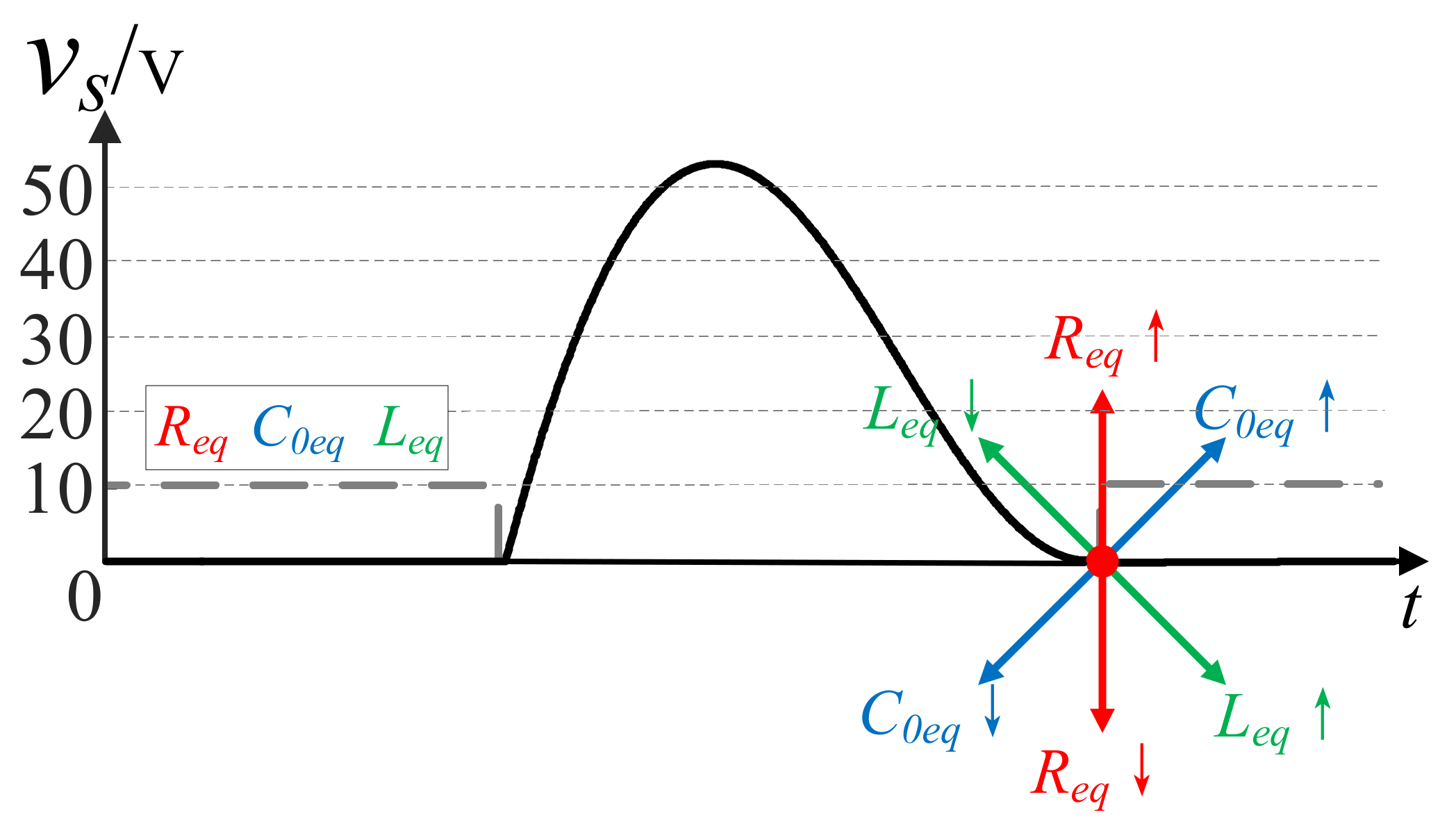
In view of the sensitive load characteristics of the class E inverter, when the equivalent load Req is greater than the optimal load Ropt, the class E inverter is in the hard-switching state. At this time, it is necessary to optimize the topology equivalent parameters to reduce the turn-on voltage and switch loss. Based on the analysis of the relationship between the switching voltage waveform and the topological parameters as well as the coupling coefficient, it can be concluded that:
(1)
When Req is too large, the soft-switching margin can be increased by adjusting C0 and L1.
(2)
Similarly, when the switch is in the hard-switching state, reducing the coupling coefficient k between the source coils of the WPT system can reduce the Req and achieve the soft switching.
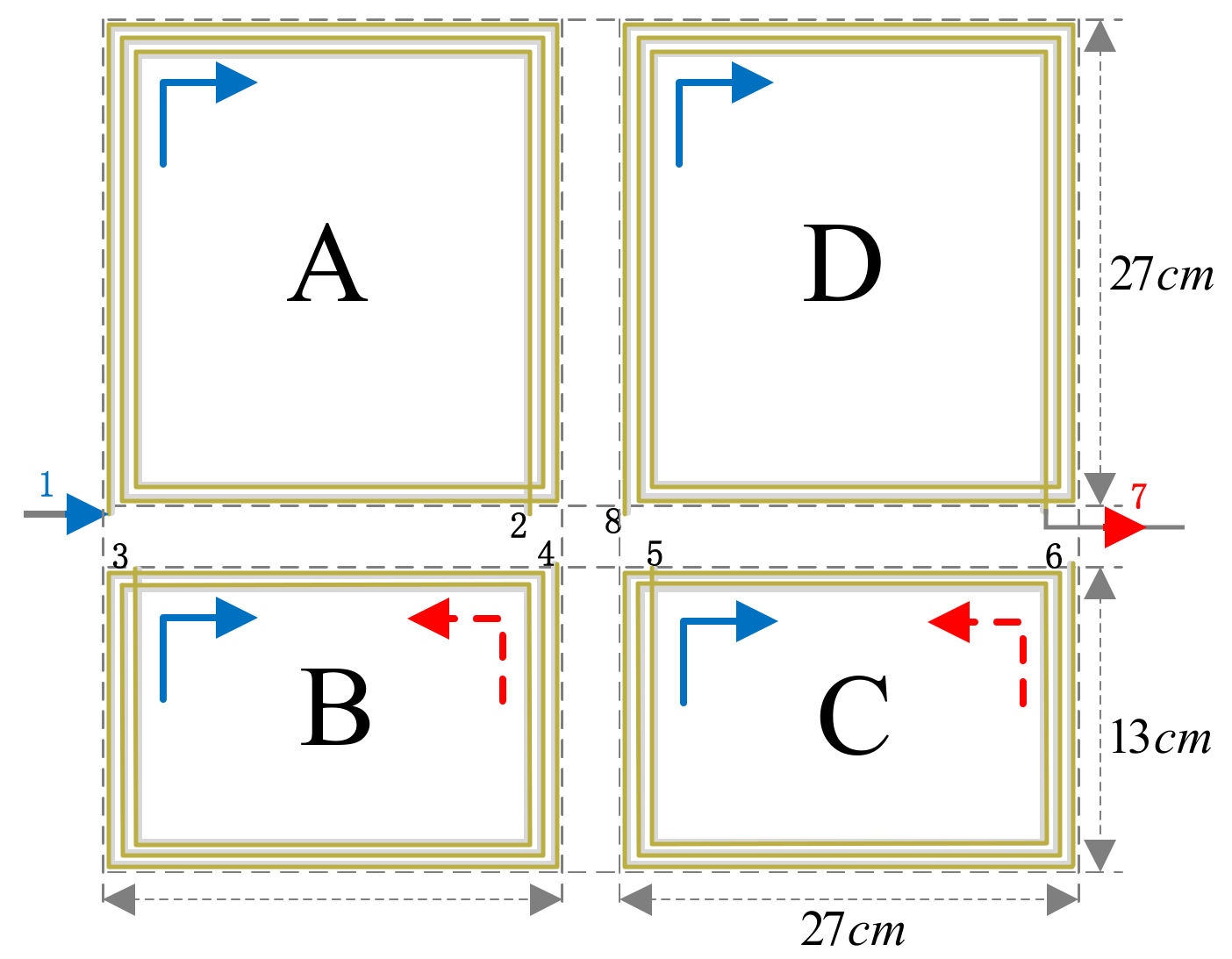
Considering that the transmitting coils are in series with multiple coils, the WPT system has the following changes when the transmitting sub-coils are connected in series and reverse:
(1)
The direction of the magnetic field of the adjusted coil is reversed, and the coupling coefficient k changes accordingly.
(2)
Due to the change of the magnetic field direction of the coil, the self-inductance L1 of the transmitting coil is affected by the change of the self-inductance between the sub-coils.
Therefore, for this paper, we designed a coil structure with multiple coils in series on the primary side. When the equivalent load was too large, on the basis of reducing the parallel capacitance C0, the primary side multi-coils were adjusted in series and reverse connection. A wide range of soft switching of the class E inverter in WPT was achieved by self/mutual inductance regulation of the primary coil. From the perspective of coil structure, an improved scheme is proposed in combination with changes in network parameters and coupling coefficients.

3.2. Analysis of the Multi-Coil Series Theory Model

When the transmitting coil is a series connection of N coils, the equivalent circuit is idealized as shown in Figure 5.
In the figure, V0 is the high-frequency power supply, VR is the sum of the source and load mutual inductance voltages at the receiving end, VA is the sum of the mutual inductance voltages between the transmitting coils, and VB is the sum of the source and load mutual inductance voltages at the transmitter. In order to simplify the calculation, assuming that the equivalent self inductance Lteq and Ct of the transmitting coil are completely resonant, the cross-mutual inductance between the transmitting coils is sorted out, and the matrix is as follows:
M 11 M 12 M 1 N M 21 M 22 M 2 N M N 1 M N 2 M N N I T I T I T I T = V A j ω
The mutual inductance values on the main diagonal are all zero, and the mutual inductance values in the upper and lower triangles are symmetrical. It can be further sorted out as follows:
V R = j ω i = 1 n M r i 1 I T V A = 2 j ω i = 1 n 1 j = i + 1 n M i j I T V B = j ω i = 1 n M r i 1 I R
Considering the coupling mutual inductance of N coils in series:
V 0 0 = 2 j ω i = 1 n 1 j = i + 1 n M i j + R T j ω i = 1 n M r i 1 j ω i = 1 n M r i 1 R + R l o a d I T I R
According to the mutual inductance range of N coil series transmitting end:
j ω M T = 2 j ω i = 1 n 1 j = i + 1 n M i j
The equivalent emission inductance is obtained as follows:
L e q = i = 1 n L n ± 2 i = 1 n 1 j = i + 1 n M i j
According to Equation (7), the self/mutual inductance adjustable range in the ideal state can be obtained, and the actual self/mutual inductance regulating range is constrained by the coil structure adopted.

3.3. Actual Coil Design

In order to achieve the wide-range soft-switching effect under the self/mutual inductance regulation mode, the design of the transmitting coil is shown in Figure 6.
The Litz wire used in the coil is twisted together by 200 strands of enameled wire, each with a diameter of 0.1 mm. The coil is tightly wound from the outside to the inside. The reference current direction of the A and D coils is limited by the port, and they all flow in one direction; the B and C coils are controlled by eight switches, and the current reference directions are both bidirectional. In the WPT system based on a class E inverter, A and D coils play the main coupling part in the coupling mechanism; B and C, as auxiliary coils, play a soft-switching adjustment function role in the inverter side of the system and approach the optimal efficiency point through the change of coupling relationship at the coupling mechanism side.
Using this coil structure, the total inductance of the resonant circuit is composed of four coils in series. Combined with the analysis of coil winding direction and mutual inductance variation range, the self inductance ratio of four small coils is set at 20:2:1:15 in turn. The parameter design can achieve wide-range soft switching, and has little influence on the coupling coefficient in the process of adjustment.
The switch control block diagram is shown in Figure 7. The reference direction of the current of the B and C coils is controlled by the switching of switches S1 to S8, and the magnetic field direction of the coil is changed to obtain the fine adjustment of the equivalent self inductance Lteq and mutual inductance of the transmitting coil. Taking S1 as the reference, the left is the a path, and the right is the b path.
Ansoft Maxwell software 16.0 was used to analyze the magnetic field distribution of the square coil in Figure 6, and the magnetic density vector diagram of the square coil shown in Figure 8 is obtained. According to the magnetic density vector diagram in Figure 8, the magnetic field distribution of the square coil is relatively uniform, and the magnetic induction line is perpendicular to the conductor. Although the magnetic density of the four corners is high, the total magnetic flux is small, so the magnetic field of the square coil can be regarded as parallel to the conductor distribution.
After simplification, the cross-mutual inductance of coils A and C and coils B and D can be ignored. The mutual inductance of the diagonal coils can be regarded as zero; only the influence between adjacent coils needs to be considered.
The mutual inductance compensation scheme is shown in Table 2. Four different mutual inductance values can be obtained by switching the switch mode, and the most suitable state is selected for compensation.
Table 2 shows the mutual inductance compensation value ΔM under different switching modes, and A and B are the switch conduction paths; according to Figure 8, MAC and MBD in the adjustable mutual inductance value are spatially symmetrical, which are not shown in Table 2.
According to Table 2 and Figure 8, switches 1-4 and 5-8 are two switch groups, and the switches in each switch group have the same switch state and path selection. This is because switches 1-4 control coil B current direction and switches 5-8 control coil C current direction. The switch state of the control switch group corresponding to each coil is determined by the first switch, thus reducing the complexity of switch control.
When the relative position of the coils is symmetrical, the coupling coefficient is idealized, and the coupling coefficient k of cross-mutual inductance is regarded as the same value. According to the proportion of the inductance value of each sub-coil, the mutual inductance relationship can be obtained.
M A B = k 20 L C * 2 L C M A D = k 20 L C * 15 L C M B C = k 2 L C * L C M C D = k L C * 15 L C
In order to ensure the soft-switching state on the inverter side, the excessive Zeq (or k) is compensated by self/mutual inductance adjustment. At this time, the magnetic field is slightly offset by the influence of the switching mode due to the compensation coil. By measuring the coupling parameter changes of the above coil structure in the adjustment process, it can be seen that the effective coupling coefficient decreases after compensation. The effective coupling coefficient changes, and the corresponding equivalent load changes under the three compensation modes are shown in Table 3. kopt and Ropt are tracked from the perspective of the coupling mechanism, and the soft-switching range is further increased.

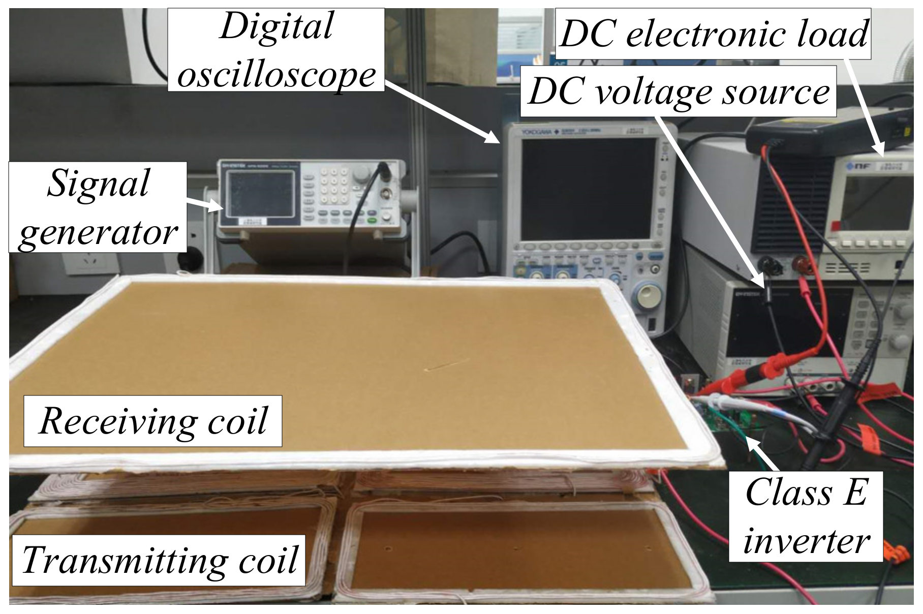
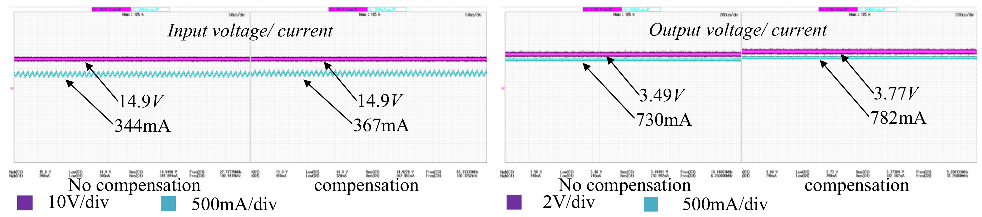
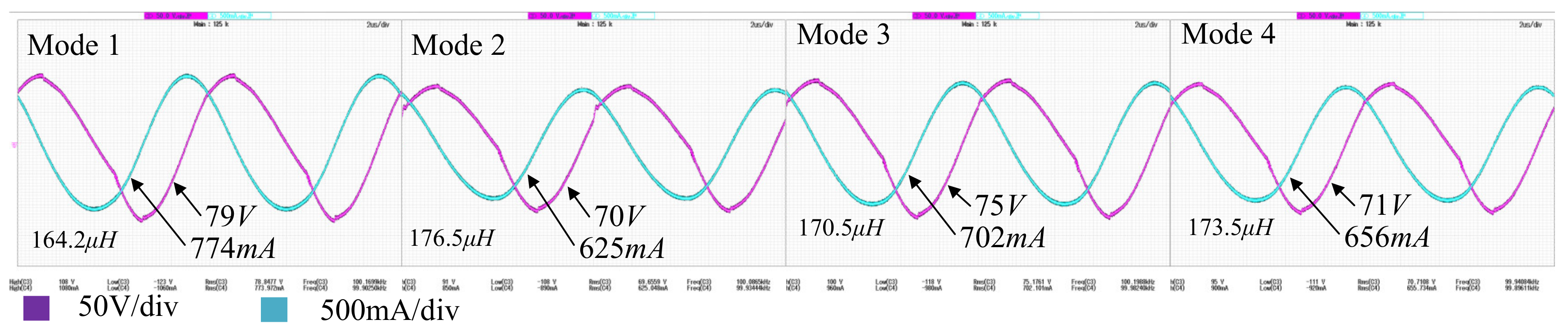
4. Simulation and Experimental Results

According to the basic topology in Figure 1, the WPT system prototype was built. The system compensation control block diagram is shown in Figure 9. First, the equivalent resistance load value was calculated by collecting the voltage and current data at both ends of the load network. Second, we judged whether the equivalent load was greater than the ideal load by judge #1. If it was greater than the ideal load, we adjusted the switch SS in the diagram to make C0 and C01 in series, and selected the compensation method through the compensation range (judge #2) in Table 3.
Finally, the transmitting coil was controlled according to the judgment result. The experimental equipment and structure are shown in Figure 10. In the class E inverter, S is an IRF740 N-channel MOSFET (Vishay, Malvern, PA, USA), and the diodes in the rectifier circuit are SS14 Schottky types (ON Semiconductor, Shenzhen, China).
The parameters of the experimental platform are shown in Table 4:
In the table, Udc is the power supply voltage, f is the switching frequency, C0 is the MOSFET shunt capacitor, C01 is the compensation switching capacitor, LA, LB, LC, and LD are the transmitting sub-coils, r1 and r2 are the AC internal resistance of the transmitting and receiving coils, C1 is the primary compensation capacitor, L2 is the receiving coil, which is designed in a square shape with the same length and width as the transmitting coil, C2 is the compensation capacitance of the receiving coil, Ropt is the optimal load of the inverter, and Rload is the actual load of the secondary side.
The mutual inductance between sub-coils is measured by an impedance analyzer, and the coupling coefficient is determined as kt = 0.0629. C01 is connected in series to the back end of C0 through the switch as the switching point of compensation state. The Leq of the four modes under the coupling coefficient can be obtained through the parameters in Table 4 and Equation (9), in which mode 1 is the normal operation state, and the other modes are the compensation state of the auxiliary coil:
mode 1 : L e q = 164.2 μ H mode 2 : L e q = 176.5 μ H mode 3 : L e q = 170.5 μ H mode 4 : L e q = 173.5 μ H
Figure 11a shows the simulation of switch voltage waveform before and after compensation for the class E inverter, and the effect before and after compensation in the figure can be seen. In the case of no compensation, ZVS and ZDS can be achieved when the equivalent load Req is equal to the optimal load Ropt, and ZVS can also be achieved when Req is less than Ropt. However, when Req is greater than Ropt, the switch-on voltage continues to rise with the increase of Req, which seriously affects the soft-switching state and leads to the increase of switching loss. Therefore, it is necessary to compensate for the case that the equivalent load Req exceeds Ropt. After compensation, all modes can achieve ZVS under the condition of 1.5 times equivalent load. According to the local enlarged drawing, when the equivalent load is 1.5Ropt and 2Ropt, the better soft-switching effect can be obtained by using mode 2 and mode 4 of the coil, respectively. After compensation, the voltage waveform of the MOSFET is improved and the switching loss is reduced. Figure 11b shows the comparison of experimental waveforms with and without compensation for 1.5 Ropt, 2Ropt, 2.3 Ropt, and 3.3Ropt. It can be seen that when Req is greater than Ropt, the MOSFET is in the hard-switching state. After being compensated by the above method, the MOSFET achieves the zero-voltage turn-on state, which is consistent with the theoretical analysis.
Figure 12 shows the voltage and current waveforms before and after compensation of the system under 2.3Ropt. It can be seen that since the input is a voltage source, the input voltage is basically unchanged before and after compensation. After compensation, the input current increased from 344 mA to 367 mA, and the system input power increased by 7%. The output voltage increased from 3.49 V to 3.77 V, the output current increased from 730 mA to 782 mA, and the system output power increased by 16%. In the case of overload, the input and output power of the system improves after compensation.
It can be seen from Figure 13 that in different compensation modes, as the actual inductance value of the transmitting coil increases, the electricity flowing through the transmitting coil decreases correspondingly, and the coil impedance increases slightly and the voltage decreases accordingly.
Figure 14 shows the efficiency and power of the inverter before and after compensation under different coupling coefficients. It can be seen from the figure that when ReqRopt, the efficiency and the power of the class E inverter are the highest. As the coupling coefficient increases, when Req is greater than Ropt, the efficiency of the inverter drops rapidly due to the influence of switching losses. At the same time, due to the deviation of the equivalent load from the optimal load, and according to the equation in Table 1, the output power decreases with the increase of the load, both of which leading to a decrease in the output power of the inverter. After self/mutual inductance compensation, the parameters of the load network after compensation increase the margin of soft switching, and the equivalent load decreases according to Table 3. The two aspects jointly achieve soft switching, reduce switching loss and equivalent load, improve inverter efficiency and power, and suppress MOSFET heating.
First, we analyzed the system efficiency comparison, as shown in Figure 15. The system efficiency of the single coil structure is basically consistent with the efficiency curve of the 4 square coil structure before compensation. In zone I, Req < Ropt, as the distance gradually gets closer, the system efficiency increases with the increase of the coupling coefficient. In zone II, when Ropt < Req, the MOSFET begins to show the hard-switching state, the self/mutual inductance switching compensation starts, but the efficiency decrease caused by switching loss is less than the efficiency improvement brought about by the increase of the coupling coefficient, so the system efficiency still rises before compensation. In zone III, 2.3Ropt < Req < 3.3Ropt (1.6Ropt to 2Ropt after compensation). In this stage, with the increase of equivalent load, the switch on voltage continues to rise, and the switching loss increases rapidly, which is greater than the efficiency improvement brought about by the coupling coefficient, leading to the efficiency decrease before compensation. In zone IV, 3.3Ropt < Req < 4.1Ropt (2Ropt to 2.5Ropt after compensation). Because the equivalent load is too large, self/mutual inductance compensation cannot fully achieve soft switching, but it can still greatly reduce the turn-on voltage. Therefore, the efficiency begins to decrease after compensation, but the efficiency is still improved compared to the uncompensated state. The coupling coefficient and equivalent load in the zones II, III, and IV are reduced after compensation, The maximum coupling coefficient (k = 0.57) and the maximum normalized load (4.1Ropt) before compensation are reduced to 0.41 and 2.5Ropt after compensation, which reduces the deviation of the equivalent load. Then, we analyzed the system output power comparison, as shown in Figure 15. When Ropt < Req, the output power of the single coil structure is slightly improved compared to the 4 square coil structure before and after compensation. With the increase of the equivalent load, when Ropt < Req, the output power of the 4 square coils before compensation and the traditional single coil structure drops rapidly. After adopting self/mutual inductance compensation, the output power of the 4 square coil structure is greatly improved compared to the traditional single coil, and the system output power is increased by 41% at 4.1Ropt.
The experimental results are consistent with the theoretical analysis. The detailed relationship and difference between the inverter efficiency and power in Figure 14 and the system efficiency and power in Figure 15 can be seen from Supplementary Materials. On the basis of this experiment, especially in the case of higher switching frequency, the switching loss continues to increase. At this time, the soft-switching state becomes more important and the compensation effect is further improved. The larger the ideal load Zopt, the smaller the proportion of reactive power consumed by the additional inductance and the active power loss caused by parasitic resistance, and the higher the system efficiency.
According to the experimental results and the above analysis, Table 5 summarizes the comparison between the self/mutual inductance compensation method and other schemes. All three methods achieve the goal of increasing load network deviation compatibility and improving efficiency. However, the self/mutual inductance compensation method does not require additional compensation components except for the switch, and the simultaneous adjustment of network parameters and coupling coefficients is achieved without increasing the complexity of the circuit. Therefore, the proposed method has more controllable parameters, lower control difficulty, and the lowest device cost.

5. Conclusions

In a wireless power transfer system based on class E inverters, changes in coupling strength and changes in load characteristics lead to hard switching of the inverter and reduce inverter efficiency. Therefore, improving the working status of the inverter can effectively enhance the system efficiency.
In this paper, we improved the structure of the inverter side coil through self/mutual inductance regulation. When the load value was greater than the optimal value, the soft-switching margin under the condition of equivalent load change was increased and the equivalent load offset was reduced, so as to achieve a wide-range ZVS from 0 to 3.3Ropt. Through experimental comparison, the overall efficiency of the system after compensation was increased by 5.625%, and the load offset before and after compensation was reduced by 39%. At the same time, in the above circumstances, this method can better improve the heating problem caused by the hard switch of the MOSFET, and improve the stability of the system operation.

Supplementary Materials

The following are available online at https://www.mdpi.com/1996-1073/13/19/5187/s1.

Author Contributions

Methodology, S.Z., J.Z., Y.W., and J.C.; validation, S.Z., L.M., and J.X.; writing—original draft preparation, S.Z., Y.W., and J.X.; writing—review and editing, S.Z., J.Z., L.M., and J.C. All authors have read and agreed to the published version of the manuscript.

Funding

This research was funded by the National Natural Science Foundation of China under Grant 51777120.

Conflicts of Interest

The authors declare no conflict of interest.

References

  1. Liping, L.; Jian, Z.; Qi, W.; Zhao, Y.; Yizhe, W.; Ying, L. Theoretical calculation and evaluation of the line losses on UHV AC demonstration project. In Proceedings of the 2015 IEEE International Conference on Cyber Technology in Automation, Control, and Intelligent Systems (CYBER), Institute of Electrical and Electronics Engineers (IEEE), Shenyang, China, 8–12 June 2015; pp. 1299–1303. [Google Scholar]
  2. Fan, Y.; Jun, L.; Bingbing, L. Design and application of integrated distribution network line loss analysis system. In Proceedings of the 2016 China International Conference on Electricity Distribution (CICED), Xi’an, China, 10–13 August 2016; pp. 1–4. [Google Scholar]
  3. Chen, B.; Xiang, K.; Yang, L.; Su, Q.; Huang, D.; Huang, T. Theoretical Line Loss Calculation of Distribution Network Based on the Integrated Electricity and Line Loss Management System. In Proceedings of the 2018 China International Conference on Electricity Distribution (CICED), Xi’an, China, 17–19 September 2018; pp. 2531–2535. [Google Scholar]
  4. Ni, L.; Yao, L.; Wang, Z.; Zhang, J.; Yuan, J.; Zhou, Y. A Review of Line Loss Analysis of the Low-Voltage Distribution System. In Proceedings of the 2019 IEEE 3rd International Conference on Circuits, Systems and Devices (ICCSD), Chengdu, China, 23–25 August 2019; pp. 111–114. [Google Scholar]
  5. Wei, X.; Wang, Z.; Dai, H.; Duong, T.P.; Lee, J.-W.; Nair, V.V.; Choi, J.R.; Jiang, C.; Chau, K.T.; Liu, C.; et al. A Critical Review of Wireless Power Transfer via Strongly Coupled Magnetic Resonances. Energies 2014, 7, 4316–4341. [Google Scholar] [CrossRef] [Green Version]
  6. Duong, T.P.; Lee, J.-W. A Dynamically Adaptable Impedance-Matching System for Midrange Wireless Power Transfer with Misalignment. Energies 2015, 8, 7593–7617. [Google Scholar] [CrossRef] [Green Version]
  7. Jiang, C.-Q.; Chau, K.-T.; Liu, C.; Lee, C.H.T. An Overview of Resonant Circuits for Wireless Power Transfer. Energies 2017, 10, 894. [Google Scholar] [CrossRef]
  8. Nair, V.V.; Choi, J.R. An Efficiency Enhancement Technique for a Wireless Power Transmission System Based on a Multiple Coil Switching Technique. Energies 2016, 9, 156. [Google Scholar] [CrossRef] [Green Version]
  9. Liu, C.; Hu, A.P.; Nair, N.-K.C. Modelling and analysis of a capacitively coupled contactless power transfer system. IET Power Electron. 2011, 4, 808. [Google Scholar] [CrossRef]
  10. Whittingham, M.S. History, evolution, and future status of energy storage. Proc. IEEE 2012, 100, 1518–1534. [Google Scholar] [CrossRef]
  11. Chen, J. Recent progress in advanced materials for lithium ion batteries. Materials 2013, 6, 156–183. [Google Scholar] [CrossRef] [PubMed]
  12. Chen, J.; Thangadurai, V. Frontiers of energy storage and conversion. Inorganics 2014, 2, 537–539. [Google Scholar] [CrossRef]
  13. Fu, M.; Yin, H.; Liu, M.; Ma, C. Loading and Power Control for a High-Efficiency Class E PA-Driven Megahertz WPT System. IEEE Trans. Ind. Electron. 2016, 63, 6867–6876. [Google Scholar] [CrossRef]
  14. Liu, M.; Fu, M.; Ma, C. Parameter Design for a 6.78-MHz Wireless Power Transfer System Based on Analytical Derivation of Class E Current-Driven Rectifier. IEEE Trans. Power Electron. 2015, 31, 4280–4291. [Google Scholar] [CrossRef]
  15. Yeh, C.; Lin, Y.; Kuo, C.; Huang, C.; Xie, C.; Lu, S.; Yang, W.; Chen, K.; Liu, K.; Lin, Y. A 70 W and 90% GaN-based class-E wireless-power-transfer system with automatic-matching-point-search control for zero-voltage switching and zero-voltage-derivative switching. In Proceedings of the 2018 IEEE International Solid—State Circuits Conference—(ISSCC), San Francisco, CA, USA, 11–15 February 2018; pp. 138–140. [Google Scholar]
  16. Kazimierczuk, M.; Bui, X. Class E DC/DC converters with an inductive impedance inverter. IEEE Trans. Power Electron. 1989, 4, 124–135. [Google Scholar] [CrossRef]
  17. Huang, X.; Chen, W. WPT topology scheme with dual parallel-circuit class E inverters and integrated inductor. In Proceedings of the 2014 International Power Electronics and Application Conference and Exposition, Shanghai, China, 5–8 November 2014; pp. 635–638. [Google Scholar]
  18. Aldhaher, S.; Luk, P.C.-K.; Whidborne, J.F. Tuning Class E Inverters Applied in Inductive Links Using Saturable Reactors. IEEE Trans. Power Electron. 2013, 29, 2969–2978. [Google Scholar] [CrossRef] [Green Version]
  19. Ayachit, A.; Corti, F.; Reatti, A.; Kazimierczuk, M.K. Zero-Voltage Switching Operation of Transformer Class-E Inverter at Any Coupling Coefficient. IEEE Trans. Ind. Electron. 2018, 66, 1809–1819. [Google Scholar] [CrossRef]
  20. Aldhaher, S.; Yates, D.C.; Mitcheson, P.D. Load-Independent Class E/EF Inverters and Rectifiers for MHz-Switching Applications. IEEE Trans. Power Electron. 2018, 33, 8270–8287. [Google Scholar] [CrossRef] [Green Version]
  21. Roslaniec, L.; Jurkov, A.; Al Bastami, A.; Perreault, D.J. Design of Single-Switch Inverters for Variable Resistance/Load Modulation Operation. IEEE Trans. Power Electron. 2014, 30, 3200–3214. [Google Scholar] [CrossRef] [Green Version]
  22. Suetsugu, T.; Kazimierczuk, M. Design procedure of class-E amplifier for off-nominal operation at 50% duty ratio. IEEE Trans. Circuits Syst. I: Regul. Pap. 2006, 53, 1468–1476. [Google Scholar] [CrossRef]
Figure 1. Wireless power transfer (WPT) system based on a class E inverter.
Energies 13 05187 g001
Figure 2. Idealized waveform of the class E inverter.
Energies 13 05187 g002
Figure 3. Voltage waveform comparison of switch under different parameter changes: (a) waveform under different Req conditions; (b) waveform under different Leq conditions; (c) waveform under different C0 conditions.
Energies 13 05187 g003
Figure 4. Influence of network parameters on the voltage waveform of the switch.
Energies 13 05187 g004
Figure 5. Source charge cross-coupling graph for primary side N coil.
Energies 13 05187 g005
Figure 6. Multi-coil series structure.
Energies 13 05187 g006
Figure 7. Model of the variable self inductance switch group.
Energies 13 05187 g007
Figure 8. Magnetic density vector of the square coil.
Energies 13 05187 g008
Figure 9. System control block diagram.
Energies 13 05187 g009
Figure 10. WPT experimental platform.
Energies 13 05187 g010
Figure 11. Self/mutual inductance compensation simulation and experimental verification: (a) simulation of switch voltage waveform before and after compensation of the class E inverter; (b) comparison of experimental waveforms before and after compensation under 1.5Ropt, 2Ropt, 2.3Ropt, and 3.3Ropt.
Energies 13 05187 g011
Figure 12. Voltage and current waveforms before and after compensation of the system under 2.3Ropt.
Energies 13 05187 g012
Figure 13. Voltage drop on the transmitter coil in different compensation modes.
Energies 13 05187 g013
Figure 14. Comparison of inverter efficiency and power before and after compensation.
Energies 13 05187 g014
Figure 15. Comparison of system efficiency and power between this method and the traditional single square coil structure.
Energies 13 05187 g015
Table 1. Calculation equation of main device parameters.
ParameterUdcC0L1C1LX
Equation P 0 ( π 2 + 4 ) R / 8 8 / ω π ( π 2 + 4 ) R Q R / ω 1 / ( ω 2 L 1 ) π ( π 2 4 ) R / ( 16 ω )
Table 2. Mutual inductance compensation value in different switching modes.
ModeABΔM
1 S1-S8 2 ( M A B + M A D + M B C + M C D )
2S1-S8 2 ( M A B M A D M B C + M C D )
3S5-S8S1-S4 2 ( M A B M A D + M B C + M C D )
4S1-S4S5-S8 2 ( M A B M A D + M B C M C D )
Table 3. Effective coupling coefficient and equivalent load change before and after compensation.
ModesEffective Coupling CoefficientEquivalent LoadCompensation Range
Mode 20.78k0.61Req2.5Ropt < Req < 3.3Ropt
Mode 30.90k0.81ReqRopt < Req < 1.8Ropt
Mode 40.81k0.66Req1.8Ropt < 2.5Ropt
Table 4. WPT system parameters.
Parameter/UnitValueParameter/UnitValue
Udc/V15LD/μH71.68
f/kHz100r1,r20.47/0.21
C0/nF29.30C1/nF17.30
C01/nF20.13L2/μH8.415
LA/μH95.60C2/nF301.1
LB/μH9.56Ropt10
LC/μH4.78Rload5.017
Table 5. Comparison with conventional methods.
TypeReference [16]Reference [17]Proposed Self/Mutual inductance Compensation Method
EffectCompatibility range of load network parameter deviation has been improved
MethodReduce loaded quality factor and magnetic integrationAdd saturated reactorSelf/mutual inductance compensation of transmitting coil
Control parametersNoneReactance value of saturated reactorResonant inductance L1 and coupling coefficient k
Pros and cons1. Complex circuit structure
2. High cost
3. No need to control
1. Complex circuit structure
2. Need for additional devices and controls
1. Simple circuit structure
2. No need for additional compensation components
3. Simple control

