Abstract
The main aim of this paper is to analyze the influence of laser shaping of the photovoltaic cell based on its efficiency. The authors described both process of the monocrystalline photovoltaic cell manufacturing, its efficiency, and the possibilities of usage in architecture and the process of creating the photovoltaic cells of unconventional shapes by using laser technology. A method for cutting photovoltaic cells using a fiber laser was presented as well as the parameters of the laser cutting process. The described method allows cutting the massively produced silicon cells according to the predetermined trajectory. Using the proposed process parameters, satisfactory cutting edge quality, and negligible impact of the laser beam on changes in the structure of the photovoltaic cell active layers were achieved. In each cycle of structure cutting, only a small part of the material is removed (from 1 to 2 μm), and depending on the thickness, the process is repeated from 50 to 300 times. It has been shown that the efficiency of the modified cells depends on the ratio of their surface area to the laser cutting line.
1. Introduction
The photovoltaic energy industry is currently one of the fastest growing branches of world economies. The production of photovoltaic cells is increasing exponentially.
The observed increase in the production of energy from photovoltaic panels is the result of technological advances in the field of modern materials and technology, and financial outlays for research and programs dedicated to photovoltaics in many countries [1,2,3].
It is foreseen that in 2050 the world largest participation of global electricity generation will be based on solar energy [1]. The amount of produced energy depends on meteorological conditions [4,5].
The installed photovoltaic systems take up a lot of space. Therefore, especially in cities, photovoltaic (PV) panels are placed on the roofs of buildings or car parks, where they do not only work as sources of electricity, but also play the role of urban infrastructure components [6,7]. Architects try to use the emerging technical structure to create architecturally interesting artistic installations (Figure 1).
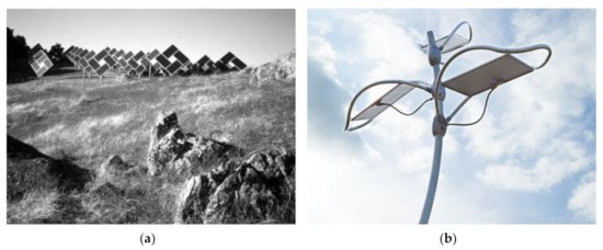
Figure 1.
Examples of PV panels applied in urban structures: (a) Solar electric sunflowers resemble nature itself. The combination of art and technology at the top of the hillside in Northern California [8]. (b) Solar flora—an artistic photovoltaic installation in the New City Schools urban garden in Southern California [9].
In the photovoltaic market, the panels that are built on the base of crystalline silicon exceed over 90% of the global production, one third of which is produced from monocrystalline silicon, while the other part from polycrystalline silicon [2].
Monocrystalline photovoltaic cells, among all kinds of silicon photovoltaic cells, are characterized by the highest efficiency but also the highest production costs [10]. The efficiency of photovoltaic cell prototypes in laboratory tests is up to 24%, while the efficiency of the mass produced 17% [2,11]. Cells made of polycrystalline silicon have lower efficiency and lower manufacturing cost than those made of monocrystalline silicon because of the absence of the costs associated with the energy-intensive single crystal manufacturing process [12,13].
Research on photovoltaic systems is still relevant today with the tendency of the world economy to reduce carbon dioxide emissions. They are being used in various locations and on various grounds. New methods are developed for placing them not only in typical locations, such as free-standing photovoltaic farms or roofs, but also in windows [14], and even on small surfaces, e.g., on textiles [15], as well the methods of producing cells with shapes different than the typical rectangular [16], or to power whole zero/low energy buildings in conditions of certainty and uncertainty forecast [17] using various optimization methods [18,19].
There are many research works in which authors modify the photovoltaic cells to increase and optimize the current module efficiency [20,21]. Improvements can be made, inter alia, more efficiently using solar spectrum in photovoltaic cells by down-conversion [22], a change of photovoltaic cell structure [23]. It is worth to study the influence of photovoltaic cell modification from different point of view among other from the point of view of modification of the photovoltaic cell edge.
Modification of the shape of photovoltaic cells is often carried out with methods borrowed from metalworking. They include mechanical cutting with a flat saw, reinforced wire, diamond discs with an external cutting circuit, and a pure water jet. Using conventional methods, it is not possible to precisely shape silicon wafers. The presented laser technology for cutting photovoltaic cells makes it possible to give any shape to cut elements, which will affect the architectural attractiveness of the designed solar devices. The laser modification of photovoltaic cells is based on laser ablation of material, and it is associated with the absorption of electromagnetic radiation, which results in a significant heating of the structure, local melting, and evaporation of the substrate. The mentioned phenomena are described by Gecys, Westin, and Pawlak’s groups [24,25,26,27]. During laser modification of photovoltaic cells, thermally induced structural local changes [28] or phase transitions to the metallic state [29] could be expected. This is an undesirable phenomenon, which can lead to significant photovoltaic cell efficiency losses [24]. The nanosecond lasers were not used in photovoltaic cell modification because of the high thermal effects [30]. However, the thermal effects, which occurred during modification processes by using the ultra-short pulsed laser, can be reduced in comparison to the nanosecond laser processing.
A lot of materials used in the production of photovoltaic panels, such as silicon or used metals, absorb the laser light of the correct wavelength. Shortwave or pulse wave lasers provide a low optical and thermal penetration. Delicate materials can be machined with a laser without contacting with them. Lots of the solutions and developed technologies have already been implemented in the photovoltaic industry, but the high potential of lasers means that many of them are still in the testing phase [31].
The desired thin layer of photovoltaic cell architecture is obtained by performing a lot of laser scribing on its functional layers: transparent oxide conducting layer (usually ITO), amorphous silicon layers a-Si, and metallization (Al). Lasers (Nd: YAG 1064 nm, pulses of 200 ns) are also used to isolate compact areas in photovoltaic cells [32] and recently to repair the cells with the rear contacts [33]. During processing cells with a laser, the thermal interaction between the laser beam and the substrate must be taken into account, because this can lead to cell destruction. Johnston et al. [34] writes about those phenomena and uses cold ablation for the processing of silicon.
The authors of the paper propose the laser cutting of serially manufactured photovoltaic cells for the production of architectural or marketing elements in which the use of unconventional shapes will be justified. The new developed technology, which is presented in the article, enables laser cutting of silicon cells without their destruction. The proposed method of cutting photovoltaic cells can be used for the production of elements of photovoltaic panels in which it will be necessary to use cells with shapes other than rectangular. Such panels can be used, for example, in the advertising industry and atypical, original architectural solutions.
2. Materials and Methods
2.1. Laser Shaping of Photovoltaic Cells
Up to now, photovoltaic cells have been cut using a stream of water using a waterjet device. The usage of laser technology for cutting photovoltaic panels requires proper selection of laser-beam parameters. Inadequate radiation wavelength, pulse energy, or scanning speed of the beam can cause thermal effects, which leads to the formation of remelting, short-circuiting, and damage to the panels.
Laser cutting is a direct ablative process of a single cell. Subsequently, the linking of cells in a typical (serial-parallel) way is carried out to achieve the best efficiency of the entire photovoltaic panel. The combined cells of both shapes, the unusual and the typical rectangular ones, are then subjected to a conventional glass laminating process and eventually any color on the glass top may be added.
During the experiment of laser cutting, a fiber optic laser (SPI 20P) and a beam scanner were used. The scheme of the laser stand used for cells cutting is shown in Figure 2.
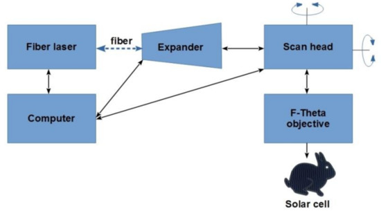
Figure 2.
System for forming the unique shape from PV elements by laser beam.
Technical specifications are listed in Table 1.

Table 1.
Parameters of the devices of the laser system.
To obtain the expected results, the parameters listed in Table 2 were used during the research.
Table 2.
Processing parameters.
The most important parameter during cells laser cutting of is the amount of energy delivered in a single pulse on a specific surface of the material (fluence in J/m2). The surface of the impact depends on the parameters of the optical system (optical fiber diameter, expander, telecentric lens). In our system, the diameter of the focused laser beam is exactly 26 µm, and it cannot be changed. The amount of energy supplied in a given area can, therefore, be regulated by changing the energy of a single pulse. In the used SPI laser, the pulse duration time is precisely defined with a predefined native frequency in the form of the so-called waveforms (wf0–wf25). For each of the 25 waveforms, the fluency in a specific range can be controlled (e.g., for wf0 from 5.37×10⁴ J/m2 to 1.07×10⁶ J/m2). The selection of the appropriate energy is related to the minimum threshold fluency below which ablation does not occur and the maximum value beyond which the processes are very violent and the cell is damaged. The threshold fluency depends among others on the type of material, used admixtures, and the type of surface. For cut cells, the boundary parameters were selected experimentally. Too much energy caused the formation of large temperature gradients, which cause high mechanical stress and cracking of the cells. When selecting the pulse energy, the aim was to minimize the heat-affected zone (HAZ) near the cut edge. HAZ can be seen in photo 5c. This is the area, which extends to about 10 µm from the cut edge, where recrystallization of the solar cell material is clearly visible. The lower energy of the pulse removes the thinner material thickness and, therefore, requires the use of more pulses scanning the surface at the same point. Applying more energy reduces the number of repetitions but increases HAZ. The selected energy value is a compromise between the duration of the cutting process (it can last from several to over a dozen minutes) and the size of the HAZ. In order to obtain the appropriate smoothness of the cutting edge, the appropriate beam scanning speed was selected, closely related to the pulse repetition frequency. The mutual dependence of these two factors affects the overlapping effect, i.e., overlapping of the laser-beam interaction areas. For the pulse repetition frequency of 35 kHz and the beam scanning speed of 200 mm/s, the interval between successive pulses is 5.7 µm. If the speed of 1000 mm/s is used for the same frequency, the distance will be 28.6 µm, which is more than the beam diameter (no overlapping). In order to obtain an appropriate smoothness of the cutting edge, the minimum distance between successive pulses must not be greater than ½ of the beam diameter (13 µm). A too-low beam scanning speed causes excessive heating of the material, which increases the heat-affected zone and increases the temperature gradient. This happens, for example, if for 35 kHz, we use a speed of 50 mm/s and the distance between the pulses is about 1.4 µm. The mentioned description of the process show that the cutting process can be done under the presented values of the laser-beam parameters.
The applied method of photovoltaic cell cutting with a nanosecond laser assumes repeated cutting with a laser beam characterized by very low energy. Depending on the thickness of the sample, it is possible to make from 50 to 200 sequentially cuts. During one cycle, the layer thickness from 1 to 10 μm is removed. The described process is longer but does not cause thermal effects.
When selecting the process parameters (mainly pulse duration, repetition rate, and beam scanning speed), attention should be paid to exposure time of the beam at one point (overlapping). During the optimization of cutting parameters, the following factors were taken into account: formation of oxide layers near the cutting edge, occurrence of short-circuits between the electrodes, and the appearance of microcracks. The occurrence of the above negative effects was verified with microscopic examination and SEM analysis. Experimental studies were supported by preliminary numerical modeling of thermal effects occurring during laser-beam interactions and experimental design techniques.
The main assumption of the presented research is to limit the thermal impact zone by reducing the maximum energy of the pulse. Limiting the pulse energy requires iterative scanning of the cell surface with a series of laser pulses repeated at a certain frequency. The laser beam is guided along the designed cutting line with the set scanning speed correlated with the pulse repetition frequency. In each cycle, only a small part of the material is removed (from 1 to 2 μm), and depending on the thickness, the process is repeated from 50 to 300 times. Although, it should be taken into account that each laser modification causes local thermal changes in structure related to the thermal nature of laser ablation [24,35]. To observe such changes the authors have chosen microscopic research, because in tomography research, the tested material should not be opaque for light [36,37,38].
2.2. Microscopic Research (SEM)
To assess the effect of laser cutting the microscopic research (SEM) was performed using scanning electron microscope—Jeol JSM-IT200 apparatus equipped with energy dispersive X-ray spectroscope Jeol JED-2300. Described apparatus with Jeol software gives possibility of simultaneous observation of morphology of the sample and chemical composition analysis. Depth of the analysis is conditioned by accelerating voltage—in case of performed analysis, it had the value of 15 kV. That gives us depth of material–electron beam electrons interaction of approximately 1.4 μm. Chemical composition is measured for all visible area, and it is the same that is visible at SEM image. The image magnification is set according to the visible sample area, and it is chosen to perform analysis only from the sample surface.
3. Experimental Results
Exemplary shapes of elements which have been cut from silicon mono- and polycrystalline cells are shown in Figure 3. During the proper work of photovoltaic panels, all cells should have two busbars. However, during conducted laboratory tests, the presence of one collecting electrode in modified photovoltaic cells did not affect the obtained efficiency.
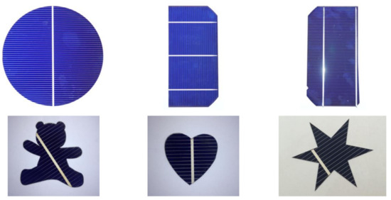
Figure 3.
Shapes of monocrystalline silicon cells that have been cut with the laser technology.
To evaluate the quality of laser cutting of photovoltaic cells SEM microscopy images were taken. The scanning microscope Hitachi S-4200 was used during the research. The image of the sample is shown in Figure 4.
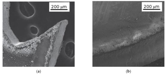
Figure 4.
SEM image of laser modified photovoltaic cells—(a) fragments of sharp point of an element and (b) the edge of the element.
The edge quality was analyzed using the microscopic images. The degree of edge equality and the condition of cell surface (closest to the cutting edge) were checked. As it is shown in Figure 4, the edge surface is not homogeneous. Its inhomogeneity is a consequence of the minor melting resulting from the laser processing with pulses of 220 ns duration and 150 kHz repetition. With the usage of shorter and lower frequencies, such heterogeneity is not observed (Figure 4b). The microscope image, which is shown in Figure 4a shows the fragment of a cut-off element where a sharp edge is obtained.
In addition, the analysis of microscopic images obtained from the Jeol JSM-IT200 microscope was performed. The chemical composition of the cell treated with the laser was analyzed. The results were compared with the chemical composition and images obtained for the sample without modification—Figure 5, Figure 6 and Figure 7. Chemical composition calculations were carried out by Jeol software, which is the part of the used scanning microscope. It was used for analyzing the obtained microscopic images in an automated manner.
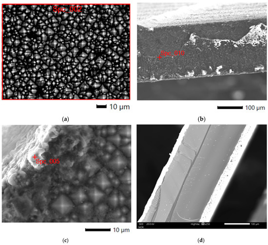
Figure 5.
SEM pictures of the surface of a monocrystalline photovoltaic cell (a) surface without laser modification (1000× magnification), (b) the point on the surface of the cutting line cross-section of the tested sample (250× magnification), (c) the point on the cell surface next to the cutting edge (magnification 2500×), and (d) the surface of the fracture (250× magnification).
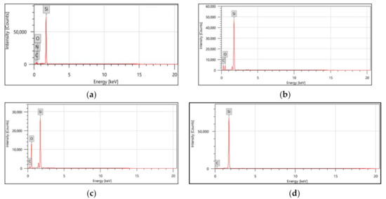
Figure 6.
Chemical composition of the monocrystalline photovoltaic cell surface (a) without laser modification, (b) the point on the surface of the cutting line, (c) the point on the surface of the cell next to the cutting edge, and (d) the point on the surface of the fracture.
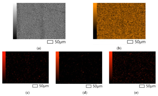
Figure 7.
Analysis of the distribution of chemical elements on the surface of the sample undergoing laser cutting. (a) SEM photo of the sample, (b) Si surface distribution, (c) C surface distribution, (d) O surface distribution, and (e) N surface distribution.
Chemical analysis of the tested surfaces (Figure 6 and Figure 7, Table 3) does not indicate the appearance of additional chemical compounds in the cell subjected to laser cutting. No additional chemical elements are observed in the spectrum obtained for the surface before and after laser cutting. The percentage of elements on the surface without modification differs in value due to the presence of nitrogen atoms on the surface of the tested sample, and the lack of this element at the tested cross-section points on the sample and on the cell surface just at the cutting edge. From the image, analysis in Figure 7 results that there is no change in the distribution of elements both at the cutting surface and on the remaining unmodified surface.
Table 3.
Chemical composition of examined samples.
Observations of the presented images from the point of view of influence of heat generated during laser treatment on changes of structure and surface of cells show lack of thermal degradation of the cells. The analysis of this photograph confirms the possibility of using a laser cutting method also in this case.
The studies conducted by the authors on electrical parameters were performed under typical STC (standard test conditions) laboratory conditions for the AM1.5G spectrum according to the International Electrotechnical Commission standard IEC 60904-1 [4,35]. Both current and voltage parameters of the cells and obtained characteristics are dependent on the length of the cutting edge and on other variables, such as layout and continuity of contacts, crystallization, and thickness of the active layers and surface area relative to the areas under the probes.
During the study, the I-U characteristics of modified samples were determined as in [39]. The I-U relationship for the reference cell was also determined as the comparative characteristics. The obtained I-U curve has been adjusted to several measured points, and graphs for exemplary monocrystalline cell (the great circle) are shown in Figure 8. The results from Figure 8 indicates that the laser cutting has no effect on the structure of the cells. Additionally, for comparison, the plot for modified and reference cells is also presented (reference cell).
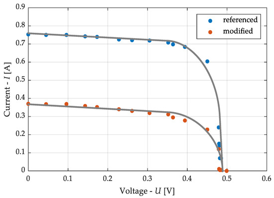
Figure 8.
The current-voltage characteristic of reference photovoltaic cell and the modified photovoltaic cell (the great circle).
Both current and voltage measurements were made with the SANWA PC5000a meter and based on the catalogue data of the meters, each time the accuracy of the measurement was calculated. It equals for the current less than 0.15% and for the voltage less than 0.1%.
The decrease in the efficiency of photovoltaic cells, which are modified with a laser beam, can be caused by overheating the material in the area of thermal impact (local damage of the cell) or short-circuit between the electrodes of the cell. The longer the laser cutting line, the greater the likelihood of damage and short-circuiting. Longer lines arise during cutting more complex shapes. In order to objectively compare more and less complex shapes, the shape factor, which equals to the quotient of the surface area of the sample and the length of the cutting edge, was introduced to the analysis.
The surface area of the specimen S, the circumference of the laser cutting edge L, and their ratio S/L are shown in Table 4. In that table, the example values obtained during the research are presented. The plot of the efficiency against the S/L ratio for examined cells is shown in Figure 9.
Table 4.
Parameters of examined samples.
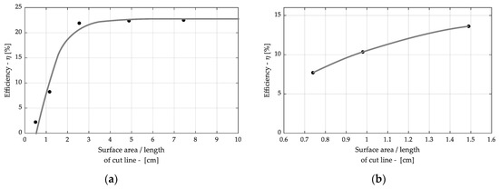
Figure 9.
Functional efficiency dependence on S/L ratio for cells after the laser cut process. (a) Monocrystalline silicon cell and (b) polycrystalline silicon cell.
As it shows in Figure 9, the longer the cut line is relative to the surface of the cell, the smaller the efficiency. From the results presented in Table 4, it can be seen that greater efficiency is obtained for shapes that have a larger S/L ratio. In samples that have this small coefficient (e.g., small circle—0.5), the efficiency is significantly lower. This is due to the appearance of overheated areas near the cut edge. In the HAZ regions, recrystallization processes occur, which cause a local change in the properties of the cell. Wide recrystallization zones arise if too-high pulse energy or too-low beam scanning speed are applied. In such a situation, the sample is overheated. For shapes with a higher S/L ratio, the HAZ zones have a lower percentage of the cut shape area, which reduces their impact on the cell’s efficiency. It is observed that, after modifying the photovoltaic cells during the presented research, there is no short-circuit between the photovoltaic cell electrodes in any of the analyzed shapes (Uoc ≠ 0). The voltage drops and the decrease in efficiency are caused only by damage of the structure near the cutting edge. A significant drop in efficiency occurs only for small elements in which the shape factor is less than one. In the case of large surfaces and short cutting edges (great circle; cell which is cut along the front electrodes), the loss of cell efficiency does not exceed 10% (the difference between 24% and 22%). The change of the cell efficiency is also influenced by the choice of the direction of the cutting line in relation to the position of the busbar (cell which is cut across the front electrodes). The decrease in polycrystalline cell efficiency is less than it is observed for monocrystalline cells.
The presented method of cutting photovoltaic cells is time-consuming, especially for parameters for which the laser beam must be scanned over 50 times. On the other hand, there is no other alternative method of cutting such complex shapes. The use of pico and femtosecond lasers will significantly extend the cutting process and at the same time will increase the costs resulting from the purchase price of such lasers. The proposed method of cutting with a fiber laser is not suitable for cutting organic cells due to the low absorption of organic materials for this wavelength (1064 nm). To increase the absorption for such a wavelength, it is necessary to use appropriate absorbers (Chromium Iron Oxide—PBr 29, Cobalt Chromite Green Spinel—PG 26, Mars black Pbk-11), which affects the properties of the cells themselves. Works on increasing the efficiency of cutting organic cells and cutting perovskite cells are under advanced research. Modification of flexible photovoltaic cells as [40] with lasers are the authors’ future plans.
4. Conclusions
The presented laser cutting method enables the adaptation of series photovoltaic cells based on mono- and polycrystalline silicon to any shape with using nanosecond laser. Thus, it can contribute to create the innovative panel shapes for architectural applications with particular emphasis on decorative ones. Only ablative cutting of semiconductor materials allow us to obtain any trajectories, including curvilinear and sharp elements. The ablative laser shape cutting was accomplished using the laser microprocessor system, whose essential elements were the source of laser radiation and the precision beam scanner. According to the presented method, the laser cutting of cells allowed us to preserve their electrical parameters, but the efficiency of the produced cells with unusual shapes is lower than the efficiency of photovoltaic cells that are available from serial production. The efficiency depends on the ratio between surface area and the length of the cutting line. The use of nanosecond laser pulses to cut photovoltaic components does not change the electrical and mechanical parameters of the cell. According to the results of the research, the small energy of a single pulse (0.42 mJ) causes only local heating of the material (a very high temperature gradient of 106 K/m), so that there are no mechanical stresses. The usage of pulses with lower energy does not cause any effects as opposed to the long lasting process. In the system the following optical limitations occur: the size of the elements cannot be greater than 120 mm and the minimum detail dimensions limit the diameter of the focused beam to 26 µm.
Author Contributions
Conceptualization, E.K. and M.T.; data curation, E.K., M.T., Ł.P. and M.H.; formal analysis, E.K., M.T., Ł.P., B.Š. and S.S.; investigation, E.K., M.T., Ł.P., B.Š., K.S. and S.S.; methodology, E.K., M.T. and S.S.; project administration, E.K. and M.H.; supervision, E.K.; validation, E.K., M.T., K.S. and S.S.; visualization, E.K.; writing—original draft, E.K. and M.T.; writing—review & editing, E.K. and M.T. All authors have read and agreed to the published version of the manuscript.
Funding
This research received no external funding.
Conflicts of Interest
The authors declare no conflict of interest.
References
- IEA—International Energy Agency. 2014. Available online: http://www.iea.org/publications/freepublications/publication/TechnologyRoadmapSolarPhotovoltaicEnergy_2014edition.pdf (accessed on 15 May 2020).
- Goetzberger, A.; Hebling, C. Photovoltaic materials, past, present, future. Sol. Energy Mater. Sol. Cells 2000, 62, 1–19. [Google Scholar] [CrossRef]
- Drzymała, A.J.; Korzeniewska, E. Profitability of solar photovoltaic investment in the light of the new act on renewable energy in Poland. Prz. Elektrotechniczny 2020, 96, 210–213. [Google Scholar]
- Nęcka, K.; Lis, S.; Dróżdż, T.; Oziembłowski, M.; Kiełbasa, P.; Tomasik, M.; Ostafin, M.; Nawara, P. Characteristics of photovoltaic power unit under variable metheorological conditions. Prz. Elektrotechniczny 2016, 12, 105–108. [Google Scholar]
- Tomasik, M.; Knaga, J.; Lis, S.; Gliniak, M. Analysis of the Effectiveness of the Prototype PV Tracking System. In Proceedings of the 2018 Applications of Electromagnetics in Modern Techniques and Medicine, PTZE 2018, Raclawice, Poland, 9–12 September 2018; IEEE: Piscataway, NJ, USA, 2018; Volume 8503095, pp. 101–104. [Google Scholar]
- Korzeniewska, E.; Drzymała, A. Photovoltaic power plants—Technical and economic aspects. Prz. Elektrotechniczny 2013, 12, 324–327. [Google Scholar]
- Tapakis, R.; Charalambides, A.G. Equipment and methodologies for cloud detection and classification: A review. Sol. Energy 2013, 95, 392–430. [Google Scholar] [CrossRef]
- Eiffert, P.; Kiss, G.J. Building-Integrated Photovoltaic Designs for Commercial and Institutional Structures A Sourcebook for Architects. Available online: https://www.nrel.gov/docs/fy00osti/25272.pdf (accessed on 15 May 2020).
- Yankodesign. Available online: http://www.yankodesign.com (accessed on 15 May 2020).
- Dobrzański, L.A.; Drygała, A.; Macek, M.; Giedroć, M. Monocrystalline silicon solar cells applied in photovoltaic system. J. Achiev. Mater. Manuf. Eng. 2012, 1, 7–13. [Google Scholar]
- Zhao, Z.; Li, P.; Wei, Y.; Lu, C.; Tan, X.; Liu, A. 17.3% efficient black silicon solar cell without dielectric antireflection coating. Sol. Energy 2014, 110, 714–719. [Google Scholar] [CrossRef]
- Parida, B.; Iniyanb, S.; Goic, R. A review of solar photovoltaic technologies. Renew. Sustain. Energy Rev. 2011, 15, 1625–1636. [Google Scholar] [CrossRef]
- Green, M.A.; Hishikawa, Y.; Warta, W.; Dunlop, E.D.; Levi, D.H.; Hohl-Ebinger, J.; Ho-Baillie, A. Solar cell efficiency tables (version 50). Prog. Photovolt. Res. Appl. 2017, 25, 668–676. [Google Scholar] [CrossRef]
- Li, Y.; Ji, C.; Qu, Y.; Huang, X.; Hou, S.; Li, C.-Z.; Liao, L.-S.; Guo, L.J.; Forrest, S.R. High Efficiency Semi-Transparent Organic Photovoltaics. In Proceedings of the IEEE 46th Photovoltaic Specialists Conference (PVSC), Chicago, IL, USA, 16–21 June 2019; pp. 98–100. [Google Scholar]
- Hatamvand, M.; Kamrani, E.; Lira-Cantú, M.; Madsen, M.; Patil, B.R.; Vivo, P.; Mehmood, M.S.; Numan, A.; Ahmed, I.; Zhan, Y. Recent advances in fiber-shaped and planar-shaped textile solar cells. Nano Energy 2020, 71, 104609. [Google Scholar] [CrossRef]
- Dharmadasa, I.M.; Roberts, J.S.; Hill, G. Third generation multilayer graded bandgap solar cells for achieving high conversion efficiencies-II. Sol. Energy Mater. Sol. Cells 2005, 88, 413–422. [Google Scholar] [CrossRef]
- Li, H.; Wang, S. Coordinated robust optimal design of building envelope and energy systems for zero/low energy buildings considering uncertainties. Appl. Energy 2020, 265, 114779. [Google Scholar] [CrossRef]
- Kasprzyk, L.; Bednarek, K. Speeding up of electromagnetic and optimization calculations by the use of the parallel algorithms. Prz. Elektrotechniczny 2009, 12, 65–68. [Google Scholar]
- Kasprzyk, L. Optimization of Lighting Systems with the use of the Parallelized Genetic Algorithm on Multi-Core Processors using the NET Technology. Prz. Elektrotechniczny 2012, 88, 131–133. [Google Scholar]
- Rauf, I.A.; Rezai, P. A review of materials selection for optimized efficiency in quantum dot sensitized solar cells: A simplified approach to reviewing literature data. Renew. Sustain. Energy Rev. 2017, 73, 408–422. [Google Scholar] [CrossRef]
- Huang, Z.; Cai, C.; Kuai, L.; Li, T.; Huttula, M.; Cao, W. Leaf-structure patterning for antireflective and self-cleaning surfaces on Si-based solar cells. Sol. Energy 2018, 159, 733–741. [Google Scholar] [CrossRef]
- De La Mora, M.; Amelines-Sarria, O.; Monroy, B.; Hernández-Pérez, C.; Lugo, J. Materials for downconversion in solar cells: Perspectives and challenges. Sol. Energy Mater. Sol. Cells 2017, 165, 59–71. [Google Scholar] [CrossRef]
- Prasad, M.R.; Kadam, V.; Joo, O.-S.; Pathan, H.M. Improving the photovoltaic parameters in Quantum dot sensitized solar cells through employment of chemically deposited compact titania blocking layer. Mater. Chem. Phys. 2017, 194, 165–171. [Google Scholar] [CrossRef]
- Gečys, P.; Markauskas, E.; Žemaitis, A.; Račiukaitis, G. Variation of P2 series interconnects electrical conductivity in the CIGS solar cells by picosecond laser-induced modification. Sol. Energy 2016, 132, 493–502. [Google Scholar] [CrossRef]
- Westin, P.-O.; Wätjen, J.T.; Zimmermann, U.; Edoff, M. Microanalysis of laser micro-welded interconnections in CIGS PV modules. Sol. Energy Mater. Sol. Cells 2012, 98, 172–178. [Google Scholar] [CrossRef]
- Pawlak, R.; Rosowski, A.; Tomczyk, M.; Walczak, M. Laser microscale technologies: Modeling assisted processes. Proc. SPIE 2013, 8703, 87030N. [Google Scholar]
- Pawlak, R.; Tomczyk, M.; Walczak, M.; Mizeraczyk, J.; Tanski, M.; Garasz, K. Selected problems in IR and UV laser micromachining of Si and GaAs in submillimeter scale. Microelectron. Eng. 2016, 151, 47–52. [Google Scholar] [CrossRef]
- Gečys, P.; Markauskas, E.; Gedvilas, M.; Račiukaitis, G.; Repins, I.; Beall, C. Ultrashort pulsed laser induced material lift-off processing of CZTSe thin-film solar cells. Sol. Energy 2014, 102, 82–90. [Google Scholar] [CrossRef]
- Hermann, J.; Benfarah, M.; Bruneau, S.; Axente, E.; Coustillier, G.; Itina, T.E.; Guillemoles, J.-F.; Alloncle, P. Comparative investigation of solar cell thin film processing using nanosecond and femtosecond lasers. J. Phys. D Appl. Phys. 2006, 39, 453. [Google Scholar] [CrossRef]
- Compaan, A.D.; Matulionis, I.; Nakade, S. Laser scribing of polycrystalline thin films. Opt. Lasers Eng. 2000, 34, 15–45. [Google Scholar] [CrossRef]
- Marie, F. Lasers Change the Shape of the Photovoltaics Industry. Photonics Spectra 2012, 46, 61–63. [Google Scholar]
- Abbott, M.D.; Trupke, T.; Hartmann, H.P.; Gupta, R.; Breitenstein, O. Laser isolation of shunted regions in industrial solar cells. Prog. Photovolt. Res. Appl. 2007, 15, 613–620. [Google Scholar] [CrossRef]
- Bovatsek, J.; Tamhankar, A.; Patel, R.; Bulgakova, N.; Bonse, J. Thin film removal mechanisms in ns-laser processing of photovoltaic materials. Thin Solid Film 2010, 518, 2897–2904. [Google Scholar] [CrossRef]
- Johnston, S.; Sulas, D.B.; Kroeger, G.F. Laser cutting and micromachining for localized and targeted solar cell characterization. In Proceedings of the IEEE 46th Photovoltaic Specialists Conference (PVSC), Chicago, IL, USA, 16–21 June 2019; pp. 2753–2757. [Google Scholar] [CrossRef]
- Markauskas, E.; Gečys, P.; Žemaitis, A.; Gedvilas, M.; Račiukaitis, G. Validation of monolithic interconnection conductivity in laser scribed CIGS thin-film solar cells. Sol. Energy 2015, 120, 35–43. [Google Scholar] [CrossRef]
- Rymarczyk, T. Electrical Capacitance Tomography and Optical Detection in Quality Control System. Prz. Elektrotechniczny 2017, 12, 211–214. [Google Scholar]
- Rymarczyk, T.; Tchorzewski, P.; Adamkiewicz, P.; Duda, K.; Szumowski, J.; Sikora, J. Practical Implementation of Electrical Tomography in a Distributed System to Examine the Condition of Objects. IEEE Sens. J. 2017, 17, 8166–8186. [Google Scholar] [CrossRef]
- Gliścińska, E.; Sankowski, D.; Krucińska, I.; Goclawski, J.; Michalak, M.; Rowinska, Z.; Sekulska-Nalewajko, J. Optical coherence tomography image analysis of polymer surface layers in sound-absorbing fibrous composite materials. Polym. Test. 2017, 63, 194–203. [Google Scholar] [CrossRef]
- Pawlak, R.; Kawczyński, R.; Korzeniewska, E.; Lebioda, M.; Rosowski, A.; Rymaszewski, J.; Sibiński, M.; Tomczyk, M.; Walczak, M. Photovoltaic cells of unconventional shapes. Prz. Elektrotechniczny 2013, 7, 288–292. [Google Scholar]
- Znajdek, K.; Szczecińska, N.; Sibiński, M.; Czarnecki, P. Energy converting layers for thin-film flexible photovoltaic structures. Open Phys. 2018, 16, 820–825. [Google Scholar] [CrossRef]
© 2020 by the authors. Licensee MDPI, Basel, Switzerland. This article is an open access article distributed under the terms and conditions of the Creative Commons Attribution (CC BY) license (http://creativecommons.org/licenses/by/4.0/).