Article

Cumulative Fatigue Damage Balancing for Modular Multilevel Converter

1
School of Electric Power Engineering, South China University of Technology, Guangzhou 510640, China
2
Science and Technology on Reliability Physics and Application of Electronic Component Laboratory, The Fifth Electronics Research Institute of Ministry of Industry and Information Technology, Guangzhou 510610, China
3
Guangdong Provincial Key Laboratory of Electronic Information Products Reliability Technology, Guangzhou 510610, China
*
Author to whom correspondence should be addressed.
Energies 2020, 13(18), 4640; https://doi.org/10.3390/en13184640
Submission received: 13 August 2020 / Revised: 30 August 2020 / Accepted: 3 September 2020 / Published: 7 September 2020
(This article belongs to the Section A1: Smart Grids and Microgrids)

Abstract

:
With many advantages, modular multilevel convert (MMC) has been extensively used in high and medium voltage power transmission projects. The thermal performance and reliability of components in MMC are key issues in system operation. However, in the current research on the reliability of MMC components, there are few methods to improve service lifetime expectancy of the components. This paper proposes a balance control algorithm, based on the cumulative fatigue damage of components, feedback to the control terminal for allocating the sub-module (SM) operating state and generating trigger pulses. Finally, the effectiveness of the proposed algorithm is verified and discussed in case studies. It is found that this algorithm is able to improve the aging degree of components in the meanwhile, the improvement in MMC reliability comes at the cost of slightly increasing capacitor voltage fluctuations and total harmonic distortion (THD). Due to the limitation of capacitor thermal performance, SM capacitor banks become a weak link in MMC reliability.

Graphical Abstract

1. Introduction

MMC is used in many medium and high voltage power occasions, which kept evolving with its unique modular structure and other technical advantages, and becomes the most popular voltage source converter [1,2]. MMC can realize DC/AC and AC/DC conversion. As long as the quantity of power modules is increased, the voltage capacity can be greatly improved, which can be well applied to high-level power transmission and distribution projects [3,4].
In China, MMC operating lifetime requirement is 45 years [5], but it is still doubtful whether it can be realized, due to its short operation time, single testing method, and lack of data. In fact, the survey found that the annual failure rate of the HVDC system is 20 times that of conventional transmission systems, 90% of which are caused by power electronic system failure [6]. Because the MMC circuit is constructed based on a large number of vulnerable SMs, its operation is susceptible to a certain SM failure. In engineering practice, although SMs on a bridge arm are connected in series, each SM of bridge arm may have certain differences as a result of various reasons [7,8], such as the installation position, capacitance tolerance, the surrounding environment, etc. From the datasheet of the capacitor manufacturer [9], it can be found that the capacitance value has an error of ±10%. That is to say, components of the same model are subjected to dissimilar degrees of stress in each SM, which results in their differences about junction temperature and lifetime.
The current MMC converter control strategy has two principal purposes: controlling the output voltage and improving the waveform quality. The control strategy mainly focuses on the modulation algorithm and the SM capacitor voltage control. At present, modulation algorithm principally includes pulse width modulation (PWM) and nearest level modulation (NLM) [10,11,12]. In fact, the output waveform of MMC is getting closer and closer to the modulated sine wave, by controlling the operation state of SM (inserted, bypassed). SM capacitor voltage control is mainly to ensure the balance of the SM voltage [13,14,15]. This is a precondition for the normal operation of the converter, which is closely related to the output voltage quality of the converter. Two capacitor voltage balancing methods are: (1) The principle of the capacitor voltage complete sorting strategy (2) The capacitor voltage balancing strategy sorted by state.
In the last five years, several studies have been conducted by researchers to improve MMC thermal performance. Frederik Hahn et al. proposed an active thermal balancing algorithm. It reduced the difference in the junction temperature spread among SMs in all operating conditions without deteriorating the performance of the system [16]. Mohammad Kazem Bakhshizadeh et al. had studied the effect of circulating current in the MMC on the loss and the thermal load of power semiconductor devices, and presented a new control strategy using circulating current to limit the magnitude of thermal cycling [17]. Jing Sheng et al. used symmetrical modulation of active bypass based on half-bridge SM (HBSM) and active thermal control strategy based on full-bridge SM (FBSM), which decreased the junction temperature of the most stressed device in HBSM and FBSM [18]. R. Picas et al. provided a new algorithm to achieve even distribution of switching losses and conduction losses in MMC, which is at the cost of slightly increasing capacitor voltage ripple [19]. Although these methods can improve MMC thermal performance, they are all indirect processes to achieve extended component lifetime. From the existing methods, the thermal performance of MMC can be improved by controlling the components’ junction temperature and power loss. Nonetheless, the cumulative fatigue damage of each SM in MMC is a blind spot during operation. They did not quantify component lifetime extension in their analysis and research. Because in most methods, component lifetime is only the final result rather than control target.
Now with the large-scale utilization of MMC, people urgently need a real time way to judge and decide the next operation based on the current SM lifetime. The operation state distribution of each SM is also not uniform. Some SMs have been inserted for a long time, while others have been in a bypassed state. Owing to the uneven distribution of SM operation state, it is found that the lifetime of SMs is greatly different. This can be said to be a waste of resources for some SMs with low utilization time. As is well known, the component that fails first is the key to the lifetime of the system. If the lifetime of the component with the shortest lifetime can be extended, this is of great significance to the system reliability. In addition, it is still a challenge to effectively improve capacitor thermal performance and reliability.
For this purpose, the contributions of this paper are mainly as follows: First of all, a lifetime balancing algorithm based on MMC cumulative fatigue damage is proposed. The algorithm combines the real time rain-flow counting algorithm to feed back the SM fatigue damage to the control terminal in real time. Fatigue damage of components will no longer be a blind spot for control. Secondly, the difference among the cumulative fatigue damage balancing algorithm and other algorithm is compared and analyzed, as well as the issues to be considered when putting it into practical application. In addition, the selection of algorithm parameters is briefly introduced. The cumulative fatigue damage balancing algorithm can coordinate the lifetime of multiple components, and it is found that the capacitor becomes the weak link, which limits the reliability of the MMC.
The rest of the paper is structured as follows. The Section 2 introduces the SM fatigue damage analysis. The Section 3 describes the principle and process of the novel control algorithm. The Section 4 analyzes and verifies the effectiveness of the novel proposed algorithm. The conclusion is at the end of the article.

2. SM Fatigue Damage Analysis

2.1. SM Fatigue Damage Analysis Flow

The SM fatigue damage analysis first needs to collect the mission profile of MMC operation [20,21]. Including power loss, device junction temperature, device related thermal parameters, etc. Among them, some parameters are not directly available. The junction temperature of insulated gate bipolar transistor (IGBT) and diode can be obtained by the Foster thermal circuit model, and the hot spot temperature of the capacitor can be got by the equivalent thermal circuit. Then the thermal cycles of IGBT and diode are calculated by the rain-flow counting algorithm [22,23]. For capacitors, the duration of their hot spot temperature needs to be recorded and the final cumulative fatigue damage and lifetime are calculated and analyzed by the Miner formula. The fatigue damage analysis flowchart is shown in Figure 1.

2.2. IGBT, Diode Fatigue Damage Analysis

During normal operation of MMC, the electrical characteristics of SM components cannot reach zero power loss. It takes a certain time when the component is turned on or off, and there is a saturation voltage in the component during the on-state. In the off state, current is still present in the device [24]. The power loss of the SM device mainly includes the IGBT conduction loss, switching loss, diode conduction loss, and reverse recovery loss [25]. These parameters need to be calculated by the datasheet provided by the manufacturer. The calculation formula of power loss is as follows:
P T , l o s s = P T , c o n d + P T , s w
P D , l o s s = P D , c o n d + P D , r e c
where, P T , c o n d and P T , s w are on-state loss and switching loss of the IGBT, respectively. Similarly, the total loss of the diode P D , l o s s is the sum of on-state loss P D , c o n d and reverse recovery loss P D , r e c .
Equations (1) and (2) are conducted in detail based on circuit theory in [21,26].
In order to obtain component junction temperature in real time, the junction temperature calculation method based on thermal network analysis is widely used at present. Here, a fourth-order Foster thermal circuit model is used [26,27]. The equivalent thermal circuit model is shown in Figure 2. The power losses of the IGBT and diode are used as the current source of the Foster model. The heat transfer process between the PN junction and the device case is represented by thermal impedances Z thJC _ T and Z thJC _ D . The thermal impedances of IGBT and diode Z thJC _ T and Z thJC _ D can be equivalent to thermal resistance and thermal capacitance in parallel. And RTi and τTi represent the thermal resistance, and thermal capacitance of the IGBT, RDi and τDi represent the thermal resistance and thermal capacitance of the diode, respectively. The heat transfer process between the device case and the heat sink can use the thermal impedance Z thCH _ T and Z thCH _ D . Z ha is thermal impedance of the heat sink. Ta represents the heat sink junction temperature. According to the thermal equivalent network of IGBT module, the steady-state average junction temperature of IGBT and diode, T T , j and T D , j , can be expressed as
T T , j = P T , l o s s ( i = 1 4 R T , j c i + R T , c h ) + T h
T D , j = P D , l o s s ( i = 1 4 R D , j c i + R D , c h ) + T h
T h = ( P T , l o s s + P D , l o s s ) R h a + T a
Specific thermal resistance parameters can be found in the datasheet provided by the manufacturer [28], see Table 1 for details.
After the junction temperature sequence of the device is obtained, the fatigue damage is calculated by the rain-flow counting algorithm. The detailed steps of the real time rain flow algorithm can refer to the literature [22]. The number of power cycles to failure N f can be approximated by (6). N f is related to the average junction temperature T j m and the fluctuation of the junction temperature ΔT [18]. Where the constants α , β have to be fitted by cycling tests.
N f = α · ( Δ T ) β · e E a / ( k B · T j m )
The cumulative fatigue damage (DT) of components can be obtained by adding the stresses experienced by devices under different conditions through the Miner rule [29].
D T = i = 1 n i N f , i
In this equation, N f , i is the number of cycles to failure corresponding to the ith thermal cycle, and n i is the number of the ith thermal cycles. The device lifetime is the reciprocal of the cumulative damage for the whole year.

2.3. Capacitor Fatigue Damage Analysis

Unlike IGBTs and diodes, the lifetime of the capacitor is related to its hot spot temperature. According to the loss characteristics of the capacitor [27,29], the capacitor power loss is the sum of the losses caused by the different frequencies’ currents [23,24].
Figure 3a is a simplified equivalent circuit model of a capacitor. It consists of an ideal capacitor C, an equivalent series resistance (ESR, R E S ), and an equivalent series inductance (ESL, L E S ). Figure 3b is a thermal model of a capacitor. This model describes the relationship between power loss and hot spot temperature. Among them, R ha represents the thermal resistance of the capacitor, and the thermal capacitance C hc and C ca can ignore their influence when calculating the steady-state capacitance hot spot temperature.
According to Figure 3b, the hot spot temperature of the capacitor under steady-state conditions can be expressed as (8). In the formula, Th is the hotspot temperature of the capacitor.
T h = P c , l o s s R h a + T a
R h a = R h c + R c a
The lifetime model of the capacitor can be used as follows [30]:
L ( T h ) = L 0 ( V V 0 ) n · 2 T 0 T h 10
In the formula, V is the actual voltage of the capacitor; V0 is the test voltage. L ( T h ) is the predicted lifetime of the capacitor at a specific hot spot temperature T h ; L0 is the lifetime under test conditions; T h is the actual hot spot temperature of the capacitor (in K); T 0 is the hot spot temperature of the capacitor under the test condition. α is the voltage stress index. For MPPF-Caps, the value of n = 7–9.
This paper uses the cumulative damage theory to quantify the lifetime of SM capacitor under variable operating conditions: it is considered that capacitor age under electrothermal stress, and the fatigue damage accumulates with use time. In a small time interval Δt, which is the temperature sampling period, it is considered that the capacitor’s electrothermal stress is unchanged. According to Miner rule, the cumulative fatigue damage of the capacitor throughout the year is the sum of the fatigue damage caused by the impacts at all sampling points.
D = j = 1 N s Δ t L [ T h ( t ) ]

2.4. Device Fatigue Damage Analysis

The three-phase MMC specified in Table 2 is chosen as the case study. Each phase of the MMC is divided into two upper and lower bridge arms, and a bridge arm consists of N SMs. One SM can be regarded as a discrete voltage source, while SM and equivalent inductors are connected in series on the bridge arm. Each phase of the bridge arm outputs from the midpoint connected by the upper and lower arms. By inserted and bypassed N SMs in the upper and lower arms, the required voltage waveform is outputted.
In order to analyze the fatigue damage of SMs, a 21-level MMC simulation model was built in MATLAB/Simulink. MMC acts as an inverter to realize the function of DC/AC. The modulation of the model is NLM, which uses a capacitor-voltage balancing algorithm. MMC is symmetrical in three phases, each of which is 120 degrees different from each other, so the bridge arm of phase A is taken as an example. The other phases can refer to the same analysis method. IGBT is 5SNA 1800E330400 from ABB, and capacitor is Type 947D polypropylene film DC-link capacitors from Cornell Dubilier [9]. MMC is considered in steady-state operation, and the rated power is transmitted from DC to AC side. The power factor cos ϕ is set to 0.95.
Simulink simulation results show that the device reaches its thermal steady-state in about 2 s. Figure 4 depicts the junction temperature fluctuation of all SMs, it can be seen that the thermal stresses on the 20 SMs are different even for the same components. The thermal performance of D1 and D2 is particularly noticeable. From the enlarged view, Some SM D1s can reach a maximum junction temperature 72 °C. However, the highest junction temperature of some SM D1s is less than 68 °C. D2 also has a maximum junction temperature 63.8 °C for some SMs, and around 60 °C for some SMs. For IGBT, T2 suffers from larger junction temperature fluctuations and average junction temperature. The overall junction temperature of T2 is 15–20 °C higher than T1. The reason for this phenomenon is not only related to the MMC mission profile, but also related to the operation state of the SM. However, in voltage balancing algorithms, the single factor that determines the operation state is the capacitor voltage amplitude. MMC control generally only involves the balance of the capacitor voltage, and rarely considers the balance of the SM operation state distribution.
According to the simulation results, Figure 5 shows that for the same component in the first 10 s, 20 SMs have different degrees of fatigue damage. It can be seen that the differences between the SMs of D1, D2 are large. At the same time scale, the cumulative fatigue damage of T2 is greater than that of T1. This also corresponds to the obvious differences in the junction temperature diagrams. Due to the unbalanced stress on the components, this will eventually lead to a certain difference in their lifetime. In order to more intuitively see the dissimilarity among components, Figure 6 uses the expected lifetime as an indicator to illustrate the cumulative fatigue damage of components. T2 is the most easily damaged component. The shortest lifetime is 25.63 years, and the longest lifetime is 46.44 years. What’s even more remarkable is that the disparity between the shortest and longest lifetime of the component is huge. For example, the range of D1 is 85.37 years, and the range of D2 is 964.3 years.
Since it is the hot spot temperature that affects the capacitor lifetime, the average junction temperature within the sampling time 5 ms is taken as the hot spot temperature of Δt. Capacitor hot spot temperature and cumulative fatigue damage are shown in Figure 4e and Figure 5e. It can be seen that the junction temperature difference of the capacitor is not obvious. Capacitors have a life span of 35.32–36.37 years.
According to the results of components and SM life expectancy analysis in Figure 6 and Figure 7, it is found that there is a distinct lifetime imbalance among components. The T2 life expectancy is the shortest of the five components. From the simulation results, the SM life expectancy is determined by T2. In other words, the lifetime of the first damaged SM is 25.63 years, and the average lifetime of the SMs is 29.13 years. The shortest lifetime component, with the largest cumulative fatigue damage at the same time, is the key to affect the system lifetime. For other components with a longer lifetime, if they can be put into service more frequently, they will bear more of the stress and reduce the lifetime gap between them. This will extend the life expectancy of MMC.

3. Cumulative Fatigue Damage Balancing Algorithm

3.1. Algorithm Principle

Firstly, the temperature of the device is continuously collected and processed. And the real time rain-flow counting algorithm is used to calculate the thermal stress of each component. Cumulative fatigue damage is also constantly updated. Then, MMC control terminal changes the inserted order of SMs according to each SM fatigue damage degree. The control system reduces the priority of the operation for the components with larger cumulative fatigue damage, and increases the priority of the components with less fatigue damage. Cumulative fatigue damage is inversely proportional to lifetime. This allows shorter lifetime components to have a longer rest time, while longer lifetime components can be fully utilized. By reasonably allocating SMs operation time, the utilization time of components is improved. Ultimately, achieve the effect of extending the components lifetime.
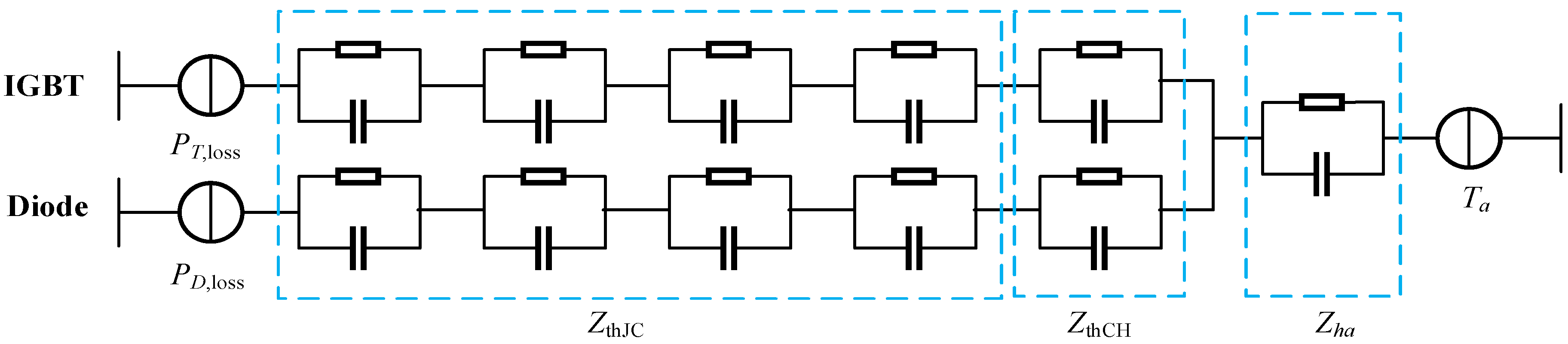
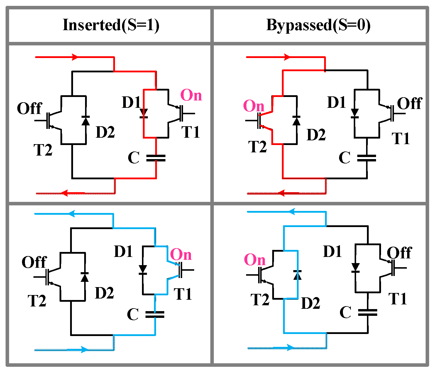
During normal operation of the MMC, the current path in the SM is shown in Figure 8. The capacitor in the SM is connected in series with T1, D1, and in parallel with T2, D2. From the path of current flow, it can be seen that when current flows T1 or D1, the capacitor is in the state of charging or discharging, respectively. Components connects in series withstand the impact of current at the same time, and the component junction temperature also increases. The SM has four operating states, in half of which the capacitor is in the inserted state. This means that the capacitor is subject to more stress than other component due to its high utilization frequency. This also explains why the hot spot temperature and fatigue damage of each SM capacitor have little difference.
Although the capacitor is one of the components in the SM, it is known from the previous analysis that their cumulative fatigue damage does not differ much. Therefore, the focus should be on thermal performance rather than cumulative fatigue damage imbalance. For this purpose, the thermal performance of the capacitor can be improved by appropriate modification control algorithm. The control method can be used to change the junction temperature to capacitor hot spot temperature by referring to the thermal balancing algorithm. The thermal performance of the capacitor is indirectly controlled by T1 and D1. This paper focuses on the method to balance the cumulative fatigue damage of the other four components.
In Figure 9, d is the number of SMs that change the operating state, non is the number of SMs that need to be inserted currently, and non-old is the number of SMs that need to be inserted at the previous moment. According to the operating principle of the SM, when the operation state of d SMs needs to be changed in the next control period.
If d is less than 0 and the bridge arm current is greater than 0, the objective function m3 is calculated, and d SMs are inserted. The current flows through T1, and the capacitors of the SMs are discharged. If d is less than 0 and the bridge arm current is less than 0, the objective function m4 is calculated, and d SMs are bypassed. The current flows through D2. If d is greater than 0 and the bridge arm current is greater than 0, the objective function m1 is calculated, and d SMs are inserted. The current flows through D1, and the capacitors of the SMs are charged. If d is greater than 0 and the bridge arm current is less than 0, the objective function m2 is calculated, and d SMs are passed. The current flows through T2. According to its objective function (12)–(15), which of the N SMs is determined to be in the n o n SMs. The specific workflow of the SM is shown in Figure 9.
When the MMC runs to time t, it calculates the value of d at this time, which indicates that there are d SMs at this time that needs to change the working state. At this moment, it is necessary to determine the SM that changes the working state according to the value of the objective function (12)–(15) of the algorithm. In formulas, v c is the capacitor voltage, DT is the cumulative fatigue damage of IGBT and diode, and α is the weight. Considering the situation of the capacitor voltage and fatigue damage, the objective function values of the 20 SMs are sorted. The smaller the value of the objective function, the higher the priority of the SM to change the working state. Because the smaller the objective function, the smaller the difference between the capacitor voltage and the voltage boundary value, the smaller, cumulative fatigue damage, and the less use of the component. Then, the first d SMs, with the smallest objective function value, are selected to switch the working components according to MMC operation requirements.
m 1 = ( v c v c , m i n ) + α 1 D T D 1
m 2 = ( v c , m a x v c ) + α 2 D T T 2
m 3 = ( v c , m a x v c ) + α 3 D T T 1
m 4 = ( v c v c , m i n ) + α 4 D T D 2

3.2. Algorithm Control Flow

The control strategy based on cumulative fatigue damage balancing combines the fatigue damage analysis of components. It feedbacks the cumulative fatigue damage of each SM to the MMC control terminal in real time. It can be seen that on the basis of Figure 1, a feedback channel is connected from the component fatigue damage to the MMC control terminal.
After the power loss of the device is transmitted to the thermal model, the component junction temperature can be obtained. The junction temperature sequence of IGBT and diode is calculated by the real time rain-flow counting algorithm. The hot spot temperature of the capacitor can be got by the thermal model, and the system records the duration of the hot spot temperature. The cumulative fatigue damage of IGBT, diode, and capacitor are constantly updated after the component lifetime model is determined. The fatigue damage value of the component is transmitted to the algorithm solver. Then, comparing the number of SMs to be inserted at this moment with the number of SMs to be inserted at the previous moment, and determining the operation state of the SM. Finally, MMC control terminal completes the allocation of the SM’s operating state and generate trigger pulses, in the light of the current direction of the bridge arm, the SM’s capacitor voltage and the device fatigue damage.

4. Case Study

4.1. Parameter Settings

To avoid more distractions, the following aspects should be considered: (1) capacitor rated voltage and voltage protection; (2) IGBT collector-emitter voltage and voltage protection; (3) the current cumulative fatigue damage of components.
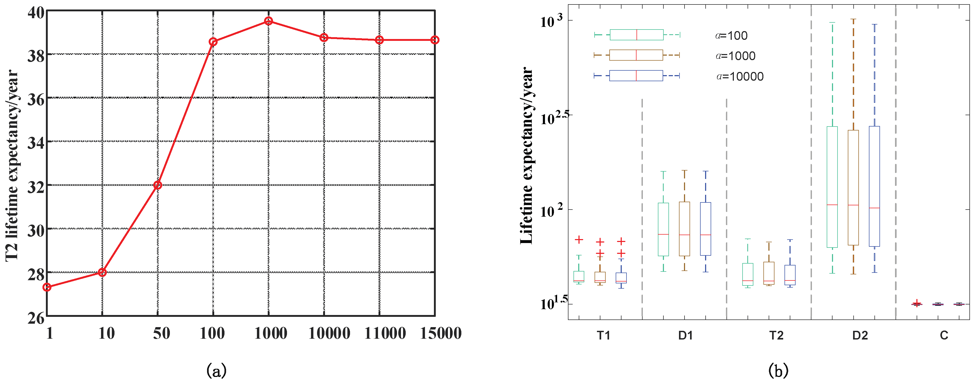
To determine the weight α in the objective function, this paper makes the following assumptions. Because T2 is the most easily damaged device, the main consideration for coefficient selection is the lifetime of T2. When the coefficient a is set to a different value, we can see the life expectancy of T2 from Figure 10a. It can be seen from the figure that when the coefficient is very small, the effect of improving the lifetime of T2 is not obvious. The control parameter (cumulative fatigue damage) did not play a major role. As the coefficient increases, the lifetime of T2 also increases. When a is greater than 10,000, because the cumulative fatigue damage is already in an absolutely large proportion, it is meaningless to continue to increase, and it is found that there is no significant change in the lifetime. So, here we focus on the situation when a = 100, 1000, 10,000. Figure 10b shows the lifetime expectancy of five components when weight α is 100,1000,10,000. As can be seen from the figure, the average lifetime expectancy of five components is not much different. When α = 100, D1 and D2 minimum lifetime expectancy is equivalent to that of α = 1000. T1′s minimum lifetime expectancy is better than the other two. When α = 1000, the maximum lifetime expectancy of T1 is less than the other weights, while the minimum lifetime expectancy is greater than or equal to the other weights. When weight α = 10,000, the minimum lifetime expectancy of all components is less than other weights, except for D2. So, effect of α = 10,000 is not as good as other weights. Since T2 is the most easily damaged component, the minimum T2 lifetime expectancy at α = 1000 is greater than the other weights, which means that it is better to improve the MMC lifetime at α = 1000.
Based on this, this paper sets α = 1000 for simulation. If the value is not appropriate, the effect of the algorithm will be affected. When the MMC is just put into operation, the DT value of each component is very small. The MMC is mainly based on the capacitor voltage balance. As time increases, the proportion of DT will increase, and the value of the weight will determine DT to what extent is gradually working. This is consistent with the actual situation. At the beginning, because the equipment is brand new, the probability of component failure is low. At this time, the balance of capacitor voltage is more important. As the use time increases, people are more concerned about the reliability of MMC, and the influence of DT will gradually increase.

4.2. Cumulative Fatigue Damage Balancing

In order to verify the correctness of the proposed active cumulative fatigue damage algorithm, a 21-level MMC three-phase simulation model is built in MATLAB/Simulink. The parameters of the MMC simulation model are set in Section 2.
Figure 11 shows the T1, T2, D1, D2, C fatigue damage of SMs. Under the proposed algorithm control, the fatigue damage of four components is decreased. Compared with Figure 5, it can be seen that the fatigue damage of the four components has been reduced to different degrees, expect for the capacitor. At the same time, T2 changed from 0.6–1.2 × 10⁻⁸ to 4–8 × 10⁻⁹, and D1 changed from 2.3–8.5 × 10⁻⁹ to 2–6.5 × 10⁻⁹. The effect of algorithm control on T2, D1 is intuitive, and the max fatigue damage is reduced by 34.61% and 21.54%, respectively. This shows that the use of control algorithms can effectively increase components’ lifetime, which has a positive impact on the reliability of SMs. The maximum and minimum cumulative fatigue damage of SMs with and without the control algorithm are discussed, respectively, for purpose of comparing the control algorithm results more clearly. In Figure 12, red, blue, green, and cyan represent the four selected SMs. The solid line represents that none algorithm control is adopted, and the dashed line indicates that the control method is adopted. It can be seen that the control method has significantly reduced the fatigue damage of the most easily damaged SM (red line), T1 SM 10, T2 SM 18, D1 SM 15 and D2 SM 7 respectively reduced by 18.13%, 38.71%, 37.43%, 74.76%. After the control, the fatigue damage of the SM with the least fatigue damage (solid blue line) increases, indicating that by changing the SMs operation priority, the utilization time of vulnerable components could be reduced, and the utilization time of idle components could be increased. As MMC continues to operate, it can be found that the component with the largest fatigue damage has changed. The most vulnerable component is the green dashed line, at this stage, they are T1 SM 14, T2 SM 1, D1 SM 14, D2 SM 20. Due to the balancing effects of the algorithm, the component with the most fatigue damage will always change. It makes the stress of the component is no longer periodic and the component participates in the assigned task more reasonably.
Compared with Figure 7, Figure 13 shows that lifetime expectancy of 20 SMs has been significantly improved. In this case, the SM of minimum lifetime expectancy is SM 20, whose lifetime expectancy is 31.13 years. The average lifetime expectancy of the SM is 31.53 years. At the SM level, the SM lifetime increased by 21.46%.

4.3. Capacitor Thermal Performance Control

From the analysis of the capacitor thermal performance and control mechanism in the second section, it can be seen that the capacitors’ junction temperature and cumulative fatigue damage are not significantly different. So, the cumulative fatigue damage algorithm has no practical significance. In addition, the voltage fluctuation range of the SM is limited, and the hot spot temperature of the capacitor does not change much, which makes the capacitor a weak link in the reliability of MMC. From a practical application point of view, consider indirectly controlling the capacitor hot spot temperature by controlling T1 and D1 through thermal balancing method [7]. Since the thermal performance difference in capacitor is small, a SM is randomly selected from the 20 SMs for reference analysis.
It can be seen from Figure 14 that after the balance algorithm is adopted, the hot spot temperature of the capacitor is reduced. Within the same two sampling time scales, the controlled hot spot temperature of the capacitors decreased by 2.27 °C and 2.35 °C. After the control, the capacitor hot spot temperature has decreased, which shows that controlling T1, D1 can change the thermal performance of the capacitor. This indicates that the thermal performance of the capacitor can be controlled by some methods. However, because T2 is the weakest link, and T1, D1 and the capacitor are interacted with each other. It is difficult for the five components to coordinate and control, so the control of the capacitor can be temporarily ignored.

4.4. Thermal Balancing and Fatigue Damage Balancing

This paper compares and analyzes the lifetime expectancy results of thermal balancing algorithm [16] and the cumulative fatigue damage balancing algorithm. The lifetime expectancy results are shown in Figure 15. The lifetime expectancy of 5 components and 20 SMs is represented by sectors with different radii. The orange in the figure represents the thermal balancing algorithm, and the blue represents the cumulative fatigue damage algorithm. And the dashed semicircle represents the average lifetime expectancy of 20 components. The minimum and maximum lifetime expectancy are marked on the graph.
For T1, the average lifetime expectancy, minimum and maximum lifetime expectancy of the fatigue damage balancing algorithm are greater than the thermal balancing algorithm. It indicates that the effect of fatigue damage balancing algorithm is slightly better than the thermal balancing algorithm, and T1 has a greater lifetime expectancy. For T2, the average lifetime expectancy of the two algorithm is basically equal. But, the minimum lifetime expectancy of the fatigue damage balancing algorithm is slightly larger than thermal balancing algorithm, and the standard deviation of fatigue damage balancing algorithm is 8.12. This illustrates that the lifetime expectancy of 20 T2 using the fatigue damage balancing algorithm is more balanced. For diodes, the D1 and D2 average lifetime expectancy of the fatigue damage balancing algorithm is greater than the thermal balancing algorithm, and the minimum lifetime expectancy of the thermal balancing algorithm D1 is greater than the fatigue damage balancing algorithm.
In terms of the algorithm application, the thermal balancing algorithm only needs to collect the component junction temperature, while the cumulative fatigue damage balancing algorithm needs to process and calculate the junction temperature, so the fatigue damage balance algorithm takes longer time. But, for the control side of the thermal balancing algorithm, the component’s cumulative fatigue damage degree is unknown. To achieve the improvement of component lifetime, by improving component’s thermal behavior is only an indirect method. There are blind spots and limitations for the realization of the ultimate goal. The cumulative fatigue damage algorithm directly feeds the fatigue damage to the control terminal, grasps the usage of each component in real time, and adjusts the component operation state. In theory, this method can more directly and effectively control the components, and finally, achieve the effect of extending components’ lifetime.

4.5. System Efficiency and Application Challenges

It can be known from the previous analysis that the algorithm can increase the device service lifetime, but whether it affects the operation requirements of the system itself also needs analysis and research. MMC main function is to approximate the required voltage waveform through the capacitor voltage. So, the capacitor voltage is an important reference parameter. In this regard, Figure 16 indicates that with the balancing algorithm control, the range of the capacitor voltage fluctuation has increased, and the charge and discharge of the capacitor voltage has been expanded from the previous 910–1190 V to 900–1240 V. The results show that the capacitor voltage fluctuation ceiling increases and the lower limit decreases. The fluctuation range of capacitor voltage is larger than before. But, the increase of capacitor voltage fluctuation basically does not affect the MMC performance. The total harmonic distortion (THD) of the cumulative fatigue damage balancing algorithm is 4.34%, which is higher than that of the capacitor voltage balancing algorithm. The THD of the capacitor voltage balancing algorithm and the thermal balancing algorithm are 3.53% and 4.29%, respectively.
In terms of simulation efficiency, based on the Simulink platform, it takes 0.013 ms to call the capacitor voltage balancing control algorithm, while the cumulative fatigue damage balancing algorithm takes 2.68 ms. This means that the realization of this algorithm has more stringent requirements for the control platform. When the number of SMs N = 20, the control cycle is usually 2 ms. FPGA can meet this requirement, and with the continuous update of technology, the algorithm can be called in a shorter time in the future.
Table 3 shows a comparison between the cumulative fatigue damage balance algorithm and the capacitor voltage balance algorithm. In terms of cost, it requires more storage space and more computing power than the voltage balancing and thermal balancing algorithm. This also means that it requires a higher configuration of hardware and software. Compared with the voltage data obtained from the voltage sensor, the algorithm also needs to calculate the junction temperature and cumulative fatigue damage in real time. This requires additional equipment investment and larger memory. Fortunately, the real time rain-flow algorithm only needs to collect the extreme points in the junction temperature rather than the whole junction temperature waveform. This takes a lot of pressure off the storage devices.
In practical engineering applications, the cumulative fatigue damage balancing algorithm is suitable for MMC projects with high reliability requirements and stricter requirements for SMs service lifetime. It can sacrifice less than 1% of THD to maximize the lifetime of SMs. In addition, it should be applied to small-scale MMC projects, due to equipment and cost reasons.

5. Conclusions

The fatigue damage distribution of the SMs and their power semiconductors in an MMC has been investigated. It has been demonstrated that the fatigue damage, due to various reasons, is unbalance among the SMs so that the SM lifetime is different. For balancing the SM lifetime, a cumulative fatigue damage balancing algorithm has been proposed to reduce the difference of SM cumulative fatigue damage and lifetime. The control algorithm enables the system to grasp the reliability of each SM in real time and feed it back to the control terminal for allocating the SM’s operating state and generating trigger pulses. Finally, the proposed model is verified in the case study.
Finally, three important conclusions can be drawn as follows:
(1)
By balancing the fatigue damage, SM resources are fully utilized so that the MMC lifetime can be effectively extended. In the case, the lifetime of the SM increased by 21.46%.
(2)
The thermal performance of the capacitor can be improved indirectly through the control of T1 and D1. If the capacitor is added into the control link, the control difficulty will be increased, and it is difficult to coordinate the five components. So, if the weakest component is not capacitor, it can be temporarily ignored.
(3)
The cumulative fatigue damage among components is achieved by sacrificing a certain degree of capacitor voltage fluctuations, which may have a certain impact on the capacitor output voltage. In addition, the algorithm has higher requirements on the hardware and software of the control system, and the cost is also higher.

Author Contributions

Conceptualization, G.W.; methodology, L.W.; software, G.O.; validation, P.Y.; investigation, P.Y.; resources, Z.Z. (Zhenwei Zhou); data curation, P.Y.; formal analysis, G.O.; writing—original draft preparation, G.O.; writing—review and editing, L.W.; supervision, G.W.; project administration, Z.Z. (Zheng Zhang); funding acquisition, Z.Z. (Zhenwei Zhou). All authors have read and agreed to the published version of the manuscript.

Funding

This research was funded by Open Research Fund of State Key Laboratory under Grant ZHD201804.

Conflicts of Interest

The authors declare no conflict of interest.

References

  1. Debnath, S.; Qin, J.; Bahrani, B.; Saeedifard, M.; Barbosa, P. Operation, Control, and Applications of the Modular Multilevel Converter: A Review. IEEE Trans. Power Electron. 2015, 30, 37–53. [Google Scholar] [CrossRef]
  2. Alyami, H.; Mohamed, Y. Review and Development of MMC Employed in VSC-HVDC Systems. In Proceedings of the 2017 IEEE 30th Canadian Conference on Electrical and Computer Engineering (CCECE), Windsor, ON, Canada, 30 April–3 May 2017; pp. 1–6. [Google Scholar] [CrossRef]
  3. Nami, A.; Liang, J.; Dijkhuizen, F.; Demetriades, G.D. Modular Multilevel Converters for HVDC Applications: Review on Converter Cells and Functionalities. IEEE Trans. Power Electron. 2015, 30, 18–36. [Google Scholar] [CrossRef]
  4. Zhao, C.; Li, Y.; Li, Z.; Wang, P.; Ma, X.; Luo, Y. Optimized design of full-bridge modular multilevel converter with low energy storage require-ments for HVDC transmission system. IEEE Trans. Power Electron. 2018, 33, 97–109. [Google Scholar] [CrossRef]
  5. Wudongde Power Station Power Transmission Guangdong Guangxi UHV Multi-terminal DC Demonstration Project DC Main Equipment Tender Technical Conditions Announcement [EB/OL]. Available online: http://www.bidding.csg.cn/zbgg/1200165613.jhtml (accessed on 19 June 2018).
  6. Zhao, Z.; Tan, D.; Li, K. Transient Behaviors of Multiscale Megawatt Power Electronics Systems—Part I: Characteristics and Analysis. IEEE J. Emerg. Sel. Top. Power Electron. 2019, 7, 7–17. [Google Scholar] [CrossRef]
  7. Hahn, F.; Buticchi, G.; Liserre, M. Active Thermal Balancing for Modular -Multilevel Converters in HVDC Applications. In Proceedings of the 2016 18th European Conference on Power Electronics and Applications (EPE’16 ECCE Europe), Karlsruhe, Germany, 5–9 September 2016; pp. 1–10. [Google Scholar]
  8. Ma, K.; Liserre, M.; Blaabjerg, F.; Kerekes, T. Thermal Loading and Lifetime Estimation for Power Device Considering Mission Profiles in Wind Power Converter. IEEE Trans. Power Electron. 2015, 30, 590–602. [Google Scholar] [CrossRef]
  9. Type 947D Polypropylene Film Capacitor, DC-Link Capacitors, online Available in Cornell Dubilier Website. Available online: http://www.cde.com/resources/catalogs/947D.pdf (accessed on 6 March 2020).
  10. Mei, J.; Shen, K.; Xiao, B.; Tolbert, L.M.; Zheng, J. A New Selective Loop Bias Mapping Phase Disposition PWM with Dynamic Voltage Balance Capability for Modular Multilevel Converter. IEEE Trans. Ind. Electron. 2013, 61, 798–807. [Google Scholar] [CrossRef]
  11. Moranchel, M.; Bueno, E.J.; Rodriguez, F.J.; Sanz, I. Implementation of nearest level modulation for Modular Multilevel Converter. In Proceedings of the 2015 IEEE 6th International Symposium on Power Electronics for Distributed Generation Systems (PEDG), Aachen, Germany, 22–25 June 2015; pp. 1–5. [Google Scholar] [CrossRef]
  12. Hu, P.; Jiang, D. A Level-Increased Nearest Level Modulation Method for Modular Multilevel Converters. IEEE Trans. Power Electron. 2015, 30, 1836–1842. [Google Scholar] [CrossRef]
  13. Liu, H.; Zhang, C.; Xu, L.; Sun, X.; Gu, S.; Li, X. Voltage Balancing Control Strategy for MMC Based on NLM Algorithm. In Proceedings of the 2019 14th IEEE Conference on Industrial Electronics and Applications (ICIEA), Xi’an, China, 19–21 June 2019; pp. 1075–1079. [Google Scholar]
  14. Wang, K.; Li, Y.; Zheng, Z.; Xu, L. Voltage Balancing and Fluctuation-Suppression Methods of Floating Capacitors in a New Modular Multilevel Converter. IEEE Trans. Power Electron. 2013, 60, 1943–1954. [Google Scholar] [CrossRef]
  15. Fan, S.; Zhang, K.; Xiong, J.; Xue, Y. An Improved Control System for Modular Multilevel Converters with New Modulation Strategy and Voltage Balancing Control. IEEE Trans. Power Electron. 2014, 30, 358–371. [Google Scholar] [CrossRef]
  16. Hahn, F.; Andresen, M.; Buticchi, G.; Liserre, M. Thermal Analysis and Balancing for Modular Multilevel Converters in HVDC Applications. IEEE Trans. Power Electron. 2018, 33, 1985–1996. [Google Scholar] [CrossRef] [Green Version]
  17. Bakhshizadeh, M.K.; Ma, K.; Loh, P.C.; Blaabjerg, F. Indirect thermal control for improved reliability of Modular Multilevel Converter by utilizing circulating current. In Proceedings of the 2015 IEEE Applied Power Electronics Conference and Exposition (APEC), Charlotte, North Carolina, 15–19 March 2015; pp. 2167–2173. [Google Scholar]
  18. Sheng, J.; Xu, H.; Li, W.; He, X.; Lin, L.; Hu, J.; Li, S. Active Thermal Control of Hybrid MMC under Over-Modulation Operation. In Proceedings of the 2018 IEEE International Power Electronics and Application Conference and Exposition (PEAC), Shenzhen, China, 4–7 November 2018; pp. 1–6. [Google Scholar]
  19. Picas, R.; Pou, J.; Zaragoza, J.; Watson, A.; Konstantinou, G.; Ceballos, S.; Clare, J. Submodule Power Losses Balancing Algorithms for the Modular Multilevel Converter. In Proceedings of the IECON 2016 42nd Annual Conference of the IEEE Industrial Electronics Society, Florence, Italy, 23–26 October 2016; pp. 5064–5069. [Google Scholar]
  20. Wang, L.; Xu, J.; Wang, G.; Zhang, Z. Lifetime estimation of IGBT modules for MMC-HVDC application. Microelectron. Reliab. 2018, 82, 90–99. [Google Scholar] [CrossRef]
  21. Du, X.; Zhang, J.; Li, G.; Tai, H.M.; Sun, P.; Zhou, L. Lifetime estimation for IGBT modules in wind turbine power converter system considering ambient temperature. Microelectron. Reliab. 2016, 65, 69–78. [Google Scholar] [CrossRef]
  22. Musallam, M.; Johnson, C.M. An Efficient Implementation of the Rainflow Counting Algorithm for Life Consumption Estimation. IEEE Trans. Reliab. 2012, 61, 978–986. [Google Scholar] [CrossRef]
  23. GopiReddy, L.R.; Tolbert, L.M.; Ozpineci, B.; Pinto, J.O.P. Rainflow Algorithm-Based Lifetime Estimation of Power Semiconductors in Utility Applications. IEEE Trans. Ind. Appl. 2015, 51, 3368–3375. [Google Scholar] [CrossRef]
  24. Yang, Y.; Ma, K.; Wang, H.; Blaabjerg, F. Mission profile translation to capacitor stresses in grid-connected photovoltaic systems. In Proceedings of the 2014 IEEE Energy Conversion Congress and Exposition (ECCE), Pittsburgh, PA, USA, 14–18 September 2014; pp. 5479–5486. [Google Scholar]
  25. Xu, J.; Wang, L.; Li, Y.; Zhang, Z.; Wang, G.; Hong, C. A unified MMC reliability evaluation based on physics-of-failure and SM lifetime correlation. Int. J. Electr. Power Energy Syst. 2019, 106, 158–168. [Google Scholar] [CrossRef]
  26. Ertrk, F.; Hava, A.M. A detailed power loss analysis of modular multilevel converter. In Proceedings of the 2015 IEEE Applied Power Electronics Conference and Exposition (APEC), Charlotte, North Carolina, 15–19 March 2015; pp. 1658–1665. [Google Scholar]
  27. Yu, Y.; Lee, T.Y.; Chiriac, V.A. Compact Thermal Resistor-Capacitor-Network Approach to Predicting Transient Junction Temperatures of a Power Amplifier Module. IEEE Trans. Compon. Packag. Manuf. Technol. 2012, 2, 1172–1181. [Google Scholar] [CrossRef]
  28. Datasheet 5SNA 1800E330400 HiPak IGBT Module. Available online: https://search.abb.com/library/Download.aspx?DocumentID=5SYA1464&LanguageCode=en&DocumentPartId=&Action=Launch (accessed on 12 April 2020).
  29. Tang, Y.; Ran, L.; Alatise, O.; Mawby, P. Capacitor Selection for Modular Multilevel Converter. IEEE Trans. Ind. Appl. 2014, 52, 2080–2087. [Google Scholar]
  30. Feng, G.; Shi, W.; Zhang, H.; Guo, L. Based on linear cumulative damage thrust rod fatigue life prediction. In Proceedings of the 2016 2nd International Conference on Control, Automation and Robotics (ICCAR), Hong Kong, China, 28–30 April 2016; pp. 249–252. [Google Scholar]
Figure 1. SM fatigue damage analysis.
Energies 13 04640 g001
Figure 2. Foster thermal model for insulated gate bipolar transistor (IGBT) and Diode.
Energies 13 04640 g002
Figure 3. Thermal model of a capacitor: (a) Simplified equivalent circuit model and (b) thermal equivalent model.
Energies 13 04640 g003
Figure 4. Components of SMs junction temperature.
Energies 13 04640 g004aEnergies 13 04640 g004b
Figure 5. Components cumulative fatigue damage.
Energies 13 04640 g005
Figure 6. Components’ lifetime expectancy.
Energies 13 04640 g006
Figure 7. SM lifetime expectancy.
Energies 13 04640 g007
Figure 8. Current paths in an SM during normal MMC operation.
Energies 13 04640 g008
Figure 9. Algorithm flowchart.
Energies 13 04640 g009
Figure 10. Weight comparison: (a) T2 lifetime expectancy; (b) Lifetime of five components.
Energies 13 04640 g010
Figure 11. Components cumulative fatigue damage.
Energies 13 04640 g011
Figure 12. Comparison of maximum and minimum cumulative fatigue damage: (a) T1 maximum and minimum cumulative fatigue damage; (b) D1 maximum and minimum cumulative fatigue damage; (c) T2 maximum and minimum cumulative fatigue damage; (d) D2 maximum and minimum cumulative fatigue damage.
Energies 13 04640 g012
Figure 13. SM lifetime expectancy.
Energies 13 04640 g013
Figure 14. Capacitor hot spot temperature.
Energies 13 04640 g014
Figure 15. Thermal balancing and fatigue damage balancing component lifetime expectancy: (a) T1 lifetime expectancy; (b) T2 lifetime expectancy; (c) D1 lifetime expectancy; (d) D2 lifetime expectancy; (e) Capacitor lifetime expectancy.
Energies 13 04640 g015
Figure 16. SM Capacitor voltage.
Energies 13 04640 g016
Table 1. Specifications of the Foster model.
DeviceParameterValue
IGBTRi (K/kW)1.6314.2862.0890.588
τi (ms)2.98648.79364.83593
DiodeRi ( K/kW)2.4414.235.0552.253
τi (ms)2.43436.51116.21641
Table 2. Specifications of the MMC system.
DescriptionValueUnit
MMC rated power20MW
DC-link voltage2000V
SMs per arm20-
SM capacitance0.013F
Arm inductor0.004H
Arm resistance0.1Ω
Grid nominal frequency50Hz
Grid voltage1000V
Grid inductance0.0046H
Grid resistance0.045Ω
Table 3. Comparisons of balancing methods.
MethodTotal Harmonic DistortionVoltage FluctuationService LifetimeHardwareSoftware
Capacitor voltage balancing [13]LowestLowestShortLowestLowest
Thermal balancing [7]MiddleHighestMiddleMiddleMiddle
Cumulative fatigue damage balancingHighestMiddleLongHighestHighest

