Article

Performance Improvement of PWM Control Methods for Voltage Step-Down in Series Resonant DC–DC Converters

Power Electronics Group, Department of Electrical Power Engineering and Mechatronics, Tallinn University of Technology, 12616 Tallinn, Estonia
*
Author to whom correspondence should be addressed.
Energies 2020, 13(17), 4569; https://doi.org/10.3390/en13174569
Submission received: 22 June 2020 / Revised: 28 August 2020 / Accepted: 31 August 2020 / Published: 3 September 2020
(This article belongs to the Section A1: Smart Grids and Microgrids)

Abstract

:
The paper is focused on galvanically isolated series resonant DC–DC converters (SRCs) with a low quality factor of the resonant tank. These converters provide input voltage regulation at fixed switching frequency and good power density. Different modulation methods at the fixed switching frequency enable the implementation of the voltage buck functionality in these converters. The SRC under study is considered as a step-up front-end DC–DC converter for the integration of renewable energy sources in DC microgrids. The paper evaluates the voltage buck performance of the SRC achieved by using different pulse-width modulation (PWM) methods including conventional PWM and shifted PWM. Moreover, the new PWM methods, i.e., the hybrid shifted PWM (HSPWM), improved shifted PWM (ISPWM), and hybrid PWM (HPWM), are proposed to overcome the disadvantages of the existing methods. They improve the power conversion efficiency in the buck mode by reducing the power losses in the semiconductor switches and the isolating transformer of the SRC. The proposed and the existing methods are benchmarked in terms of the components stresses and power conversion efficiency. The presented findings have been experimentally validated by the help of a 200 W prototype, which demonstrated the lowest power loss in the case of the HPWM.

Graphical Abstract

1. Introduction

Much attention is being paid to low-voltage DC microgrids in small-scale systems such as the power systems of buildings. The majority of consumer electronics, such as TVs, computers, lighting, and appliances, are essentially DC loads supplied directly or through a DC–DC converter from a DC microgrid [1]. Residential microgrids are usually designed with a centralized DC bus with an operating voltage of 350–400 V [2,3]. Direct-current devices, renewable energy sources, and energy storage are interfaced with the DC bus through individual DC–DC converters. PV panels, wind turbines, and fuel cells are the most commonly used residential renewable energy sources. DC microgrids are connected to the utility grid using a grid-tied inverter [4,5]. This technology facilitates realization of zero energy buildings as they require on-site energy production to offset their consumption [6]. The main advantage of the DC microgrids is the absence of double (DC–AC–DC) energy conversion between sources and loads. Moreover, the individual DC–DC converters provide a maximum power point tracking and protection functionalities for each energy source, regardless of external conditions and conditions of the microgrid [7].
Galvanic isolation between the grid and the consumers can improve safety and provide better protection of the system. Galvanic isolation can be achieved by employing a low-frequency transformer between the interface inverter and the utility grid, or a high-frequency transformer in the front-end DC–DC converter. A comparison of the two isolation approaches shows that the use of a high-frequency transformer would result in a much smaller size and weight [8,9,10].
The output voltage of renewable sources can vary in a wide range of one to six. For example, shade-tolerant residential PV applications require an input voltage range from 10 V to 60 V [11]. Other examples of applications with a wide input voltage range are railway auxiliary power supplies [12] and interface converters for small variable-speed wind turbines with a permanent magnet synchronous generator [13]. Consequently, the corresponding interface DC–DC converters must control voltage in a wide range. Many industrial DC–DC converters operate in a narrow voltage range to provide maximum efficiency. The wide input range is usually handled using two-stage energy conversion, which compromises the power conversion efficiency and reliability and increases the cost [14].
Due to the lack of standardization, DC microgrids can contain different types of DC–DC converters for each type of renewable energy source. This approach allows converter optimization, thus higher efficiency is achieved. However, it is not easy to implement the approach from an industrial point of view. Hence, costs related to the production of different types of converters slow down the deployment of DC microgrids [15]. The commercialization of a universal DC–DC converter type can greatly benefit the market of DC microgrids. These converters should provide high efficiency, galvanic isolation, and a wide range of voltage and load regulation, while they should be capable of parallel operation to increase the rated power.
The series resonant DC–DC converter (SRC) features high efficiency and galvanic isolation. Previously, they were avoided in many applications because of frequency voltage control and poor controllability at light load [16,17,18,19]. However, it was demonstrated recently that the application of SRC along with the discontinuous resonant current (DRC) implementation of the resonant tank enables various control methods with a fixed switching frequency [20]. The DRC SRC can implement the buck-boost regulation of the input voltage in a wide range while avoiding wide switching frequency variations that could result from frequency voltage control. The boost functionality requires an active boost rectifier and uses the transformer leakage inductance as the AC boost inductor [21]. The buck functionality can be implemented by applying a special modulation to the front-end inverter stage [22]. The quality factor (Q) of the resonant tank must be lower than onein any conditions to ensure the DRC operation. This means that the resonant current drops to zero when the voltage applied to the resonant tank is set to zero. Thus, the DRC could provide a soft-switching operation. Moreover, the DRC utilizes the dead-times between the commutations of the front-end switches when the transformer magnetizing current could recharge parasitic capacitances of the MOSFETs [23,24,25,26,27,28,29].
Various modulation methods have been proposed for the SRC, including the pulse-width modulation (PWM) [23], shifted PWM (SPWM) [26], the phase-shift modulation (PSM) [23,27,28], and the hybrid PSM (HPSM) [29]. Each of the methods provides an opportunity to buck (step-down) the input voltage by regulating the duration of the voltage applied to the resonant tank. All of them are applicable to the full-bridge switching cells. In addition, the PWM methods can also be used for the half-bridge front-end inverters. This study is focused on the PWM methods used in the SRC for the buck mode implementation due to universal applicability to both full- and half-bridge front-end inverters. This study further contributes to the topic of buck mode control of the SRC by analyzing the existing methods and providing closed-form expressions for the DC voltage gain for the first time. In addition, the novel improved PWM methods are synthesized and benchmarked experimentally against each other and the existing PWM methods.

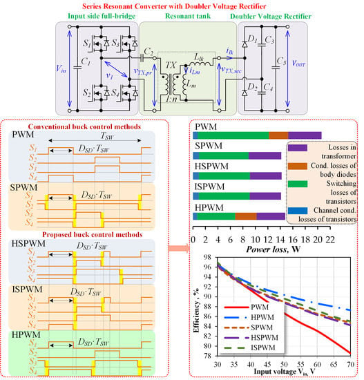
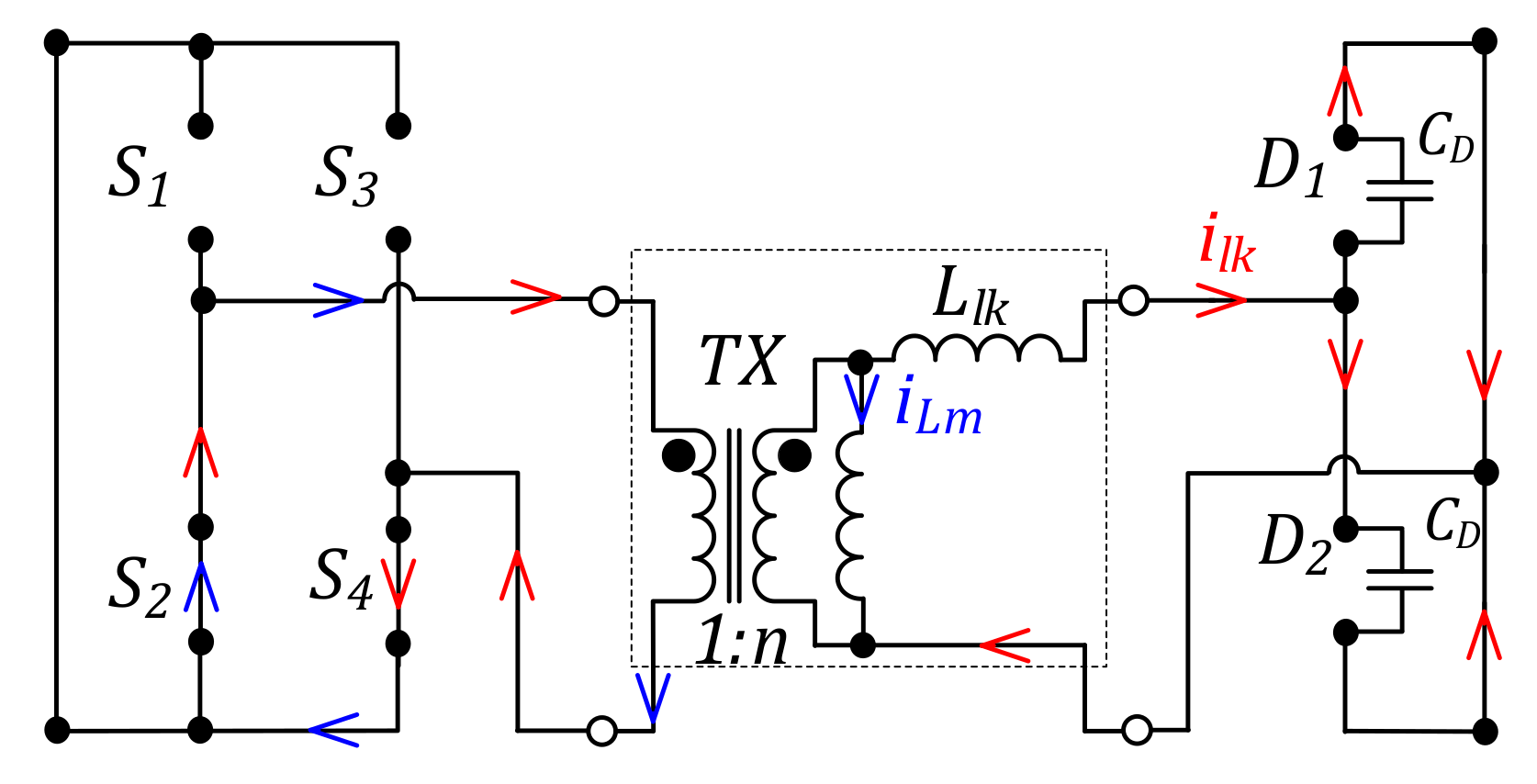
2. Description of the Series Resonant DC–DC Converter

The topology of the case study SRC is shown in Figure 1 [30]. The SRC consists of the full-bridge cell based on MOSFETs at the input side, the voltage doubler rectifier at the output side, an isolation transformer, and DC blocking capacitors in series with the transformer windings (C2, C3, and C4), which form the series resonant tank with the leakage inductance of the transformer.
The angular resonant frequency is defined as
ω r = 1 L l k C r ,
and the characteristic impedance is
Z r = L l k C r ,
where Cr is the equivalent resonant capacitance calculated as
C r = C 2 C 4 C 5 + C 3 ( C 4 + C 5 ) n 2 C 4 C 5 n 2 + ( C 3 n 2 + C 2 ) ( C 4 + C 5 ) ,
Llk is the leakage inductance of the transformer.
The blocking capacitor neutralizes any DC bias current in the isolation transformer windings, thus allowing the application of asymmetrical PWM methods. In the considered case, the topology operates under the DRC mode. Hence, the switching frequency should be 5–10% lower than the resonant frequency to implement sufficient dead-times needed for soft-switching employing the transformer magnetizing current [11].

3. Analysis of Existing PWM Methods

This section analyzes existing PWM methods in detail for buck mode realization in the SRC to determine their disadvantages and challenges. Figure 2 shows the basic waveforms of the SRC operation with the two existing modulations under study: PWM [23] and SPWM [26] methods.

3.1. Methodology

Previously, only explicit expression of the DC gain was provided for the SRC controlled with existing PWM [5] and SPWM [26] methods. The closed-form solution is not presented in the literature. Therefore, an algorithm for deriving a closed-form gain expression of the DC voltage gain is demonstrated for the PWM methods of the SRC. An ideal model of a transformer without resistances is discussed in the article as this methodology does not consider power losses.
The converter DC voltage gain normalized for the transformer turns ratio n is defined in [11]:
G = V o u t n · V i n .
However, [11] does not provide a closed-form solution for expressing Equation (4) as a function of the duty cycle DSD. The analysis of the circuit is based on the assumption of lossless components. An expression for the converter DC voltage gain can be derived using the power balance:
P i n = P o u t .
First, it is assumed that the input power equals the average power fed by the front-end inverter to the isolating transformer (ignoring the influence of the magnetizing inductance):
P i n = 1 T S W 0 T S W v 1 ( t ) n i l k ( t ) d t ,
where v1 is a piecewise-linear function of the front-end inverter voltage, ilk is a piecewise-linear function of the resonant current, TSW is the switching period.
Output power is defined by the output voltage and the load as follows:
P o u t = V o u t 2 R ,
where Vout is the average output voltage, R is the load resistance.
Considering how Equations (6) and (7) can be substituted into Equation (5), power balance takes an equation:
1 T S W 0 T S W v 1 ( t ) n i l k ( t ) d t = V o u t 2 R .
Taking into account Equation (4), an equation of the converter gain can be derived from Equation (8) analytically or numerically as a function of the converter parameters, duty cycle DSD, and the input voltage:
G = f V i n , D S D , n , R , L l k , C r , T S W .
This methodology is universal for all PWM methods considered in this paper. The only difference is how the time-functions of v1 and ilk are defined. Thus, they will be shown for each PWM method below.

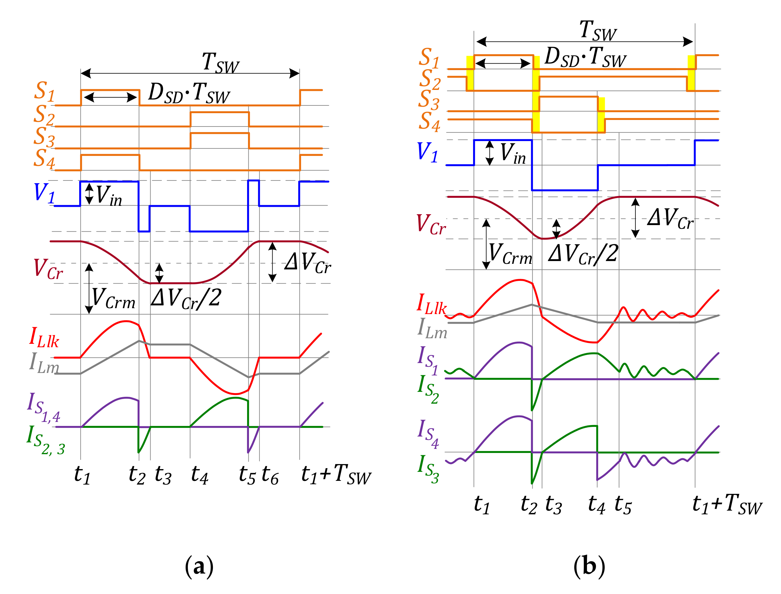
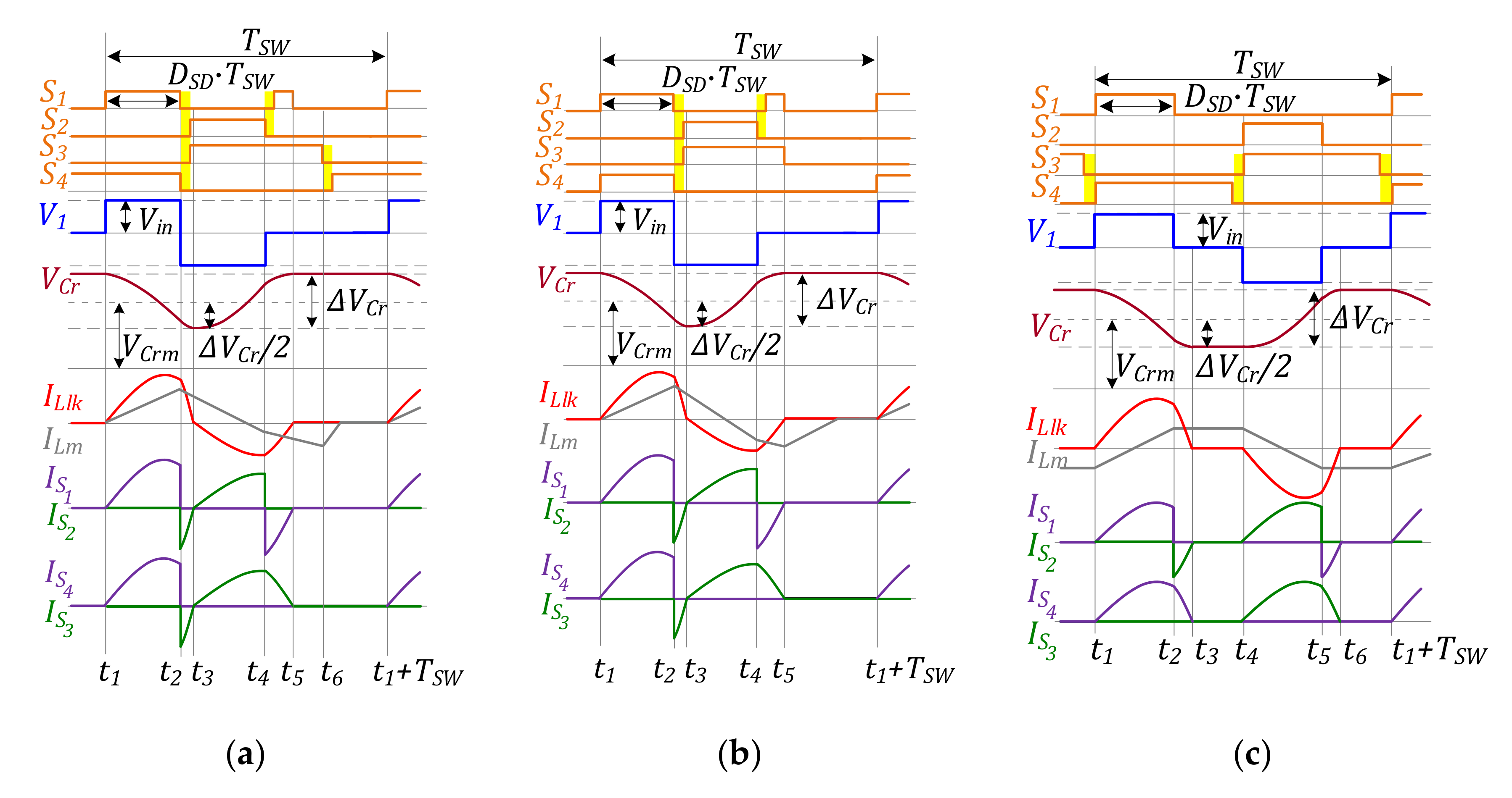
3.2. Conventional PWM Method

The basic control method is the conventional PWM [5]. It is the simplest control method for both the full-bridge and the half-bridge switching cells. The operation principle of the SRC controlled using PWM is shown in Figure 2a. The switches are turned on at zero current, but their turn-off is hard. It is a significant drawback of this modulation method. The duty cycle DSD of the diagonal switches controls the duration of the voltage pulses applied to the resonant tank. The resonant current drops to zero through the body diodes of MOSFETs when the switches are turned off. That is another marked drawback of this modulation since the body diodes of the MOSFETs S1S4 have high conduction and reverse recovery losses. All the switches operate under similar conditions when controlled with the PWM method.
A v1 can be described as a function of time for the conventional PWM method as follows:
v 1 ( t ) = V i n ,   t 1 t < t 2 ; V i n ,   t 2 t < t 3 ; 0 ,   t 3 t < t 4 ; V i n ,   t 4 t < t 5 ; V i n ,   t 5 t < t 6 ; 0 ,   t 6 t < t 1 + T S W .
In a similar way, the current ilk can be defined:
i l k ( t ) = I l k 1 · s i n ( ω r t ) ,   t 1 t < t 2 ; I l k 2 · s i n ( ω r t φ 2 ) ,   t 2 t < t 3 ; 0 ,   t 3 t < t 4 ; I l k 1 · s i n ( ω r t ) ,   t 4 t < t 5 ; I l k 2 · s i n ( ω r t φ 2 ) ,   t 5 t < t 6 ; 0 ,   t 6 t < t 1 + T S W ;
where
I l k 1 = V i n n + v C r ( t 1 ) V o u t Z r ,
I l k 2 = I l k 1 · sin ω r D S D T S W 2 + V i n · n + v C r ( ω r D S D T S W ) V o u t Z r 2 ,
φ 2 = ω r · ( t 3 t 2 ) = arcsin I l k 1 · sin ω r · D S D · T S W I l k 2 ,
and where DSD is the duty cycle of an active state.
The function of the resonant capacitor voltage can also be written as a piecewise-linear function in the PWM case:
v C r ( t ) = I l k 1 · Z r cos ( ω r t ) V i n n + V o u t ,   t 1 t < t 2 ; I l k 2 · Z r c o s ( ω r φ 2 ) 1 + V C r m Δ V C r 2 ,   t 2 t < t 3 ; V C r m Δ V C r 2 ,   t 3 t < t 4 ; I l k 1 · Z r cos ( ω r t ) + V i n n ,   t 4 t < t 5 ; I l k 2 · Z r c o s ( ω r t ) 1 + V C r m + Δ V C r 2 ,   t 5 t < t 6 ; V C r m + Δ V C r 2 ,   t 6 t < t 1 + T S W . ,
where VCrm is the median value of the resonant voltage:
V C r m = V o u t 2 ,
and ΔVCr is the cumulative peak-to-peak voltage ripple of the equivalent resonant capacitor Cr:
Δ V C r = V o u t · T S W C r · R .
Taking into account Equations (8)–(17), the normalized DC voltage gain of the SRC for the PWM method equals
G = B 1 A 1 +   B   A 1 + 1 2 + 4 A B .
There are two parameters used to simplify the equation:
A = C r R f S W ,
B = 1 cos ( ω r D S D T S W ) ,
where fSW = 1/TSW is the switching frequency.
Previously, only explicit expression of the DC gain was provided for the SRC controlled with PWM [5]. The closed-form solution (18) is presented here for the first time. In high step-up applications, the main drawback of the PWM method is high power loss associated with the use of the body diodes of the front-end MOSFETs.

3.3. Conventional Shifted PWM Method

The first step towards improved efficiency provided by the PWM method is to apply the shifted PWM (Figure 2b), as was demonstrated in [26], similar to modulation in [25]. Compared to the conventional PWM, the control signal of the switch S3 here is shifted in the vicinity of the control signal of the switch S4. Hence, they are separated by the dead-time right in the middle of the switching period. The SPWM reduces the conduction losses in the front-end MOSFETs body diodes. The power loss is reduced as the switches S1 and S4 turn off at the instant t3, which causes the body diodes of the switches S2 and S3 to conduct during a short dead-time. However, the S2 and S3 are turned on after the dead-time, which results in bypassing their body diodes through the MOSFET n-channel with much lower conduction losses. In this case, switches S2 and S3 turn on at zero voltage, which would also reduce the switching losses. The voltage applied to the transformer and the output voltage are controlled by the duty cycle of switches S1 and S2 controlled synchronously. At the instant t5, the resonant current drops to zero. Then there is the zero (freewheeling) state of the inverter, where parasitic oscillations occur between the parasitic capacitance of the rectifier diodes and the leakage inductance. These oscillations would add parasitic losses in a converter.
The time function of the voltage v1 can be described for the SPWM method as follows:
v 1 ( t ) = V i n ,   t 1 t < t 2 ; V i n ,   t 2 t < t 3 ; V i n ,   t 3 t < t 4 ; 0 ,   t 4 t < t 5 ; 0 ,   t 5 t < t 1 + T S W . .
The time function of the current ilk is described by (22) for the SPWM method:
i l k ( t ) = I l k 1 · sin ( ω r t ) ,   t 1 t < t 2 ; I l k 2 · sin ( ω r t φ 2 ) ,   t 2 t < t 3 ; I l k 3 sin ( ω r t ) ,   t 3 t < t 4 ; I l k 4 · sin ( ω r t φ 4 ) ,   t 4 t < t 5 ; 0 ,   t 5 t < t 1 + T S W ; .
where Ilk1, φ2, Ilk2 are the same as Equations (12)–(14) for the conventional PWM method.
I l k 3 = V i n n + v C r ( t 3 ) Z r ,
I l k 4 = I l k 3 · sin ω r D S D T S W 2 + v C r ( t 4 ) Z r 2 ,
φ 4 = arcsin I l k 3 · sin ω r D S D T S W I l k 4 .
A function of the resonant capacitor voltage can also be written as a piecewise-linear function in the case of the SPWM method:
v C r ( t ) = I l k 1 · Z r cos ( ω r t ) V i n n + V o u t ,   t 1 t < t 2 ; I l k 2 · Z r c o s ( ω r t φ 2 ) 1 ,   t 2 t < t 3 ; V C r m Δ V C r 2 ,   t 3 t < t 4 ; I l k 3 · Z r cos ( ω r t ) + V i n n ,   t 4 t < t 5 ; I l k 4 · Z r c o s ( ω r t φ 4 ) 1 + V C r m + Δ V C r 2 ,   t 5 t < t 6 ; V C r m + Δ V C r 2 ,   t 6 t < t 1 + T S W ; ,
where VCrm is the median value of the equivalent resonant capacitor voltage:
V C r m = n V i n n V i n c o s ( ω r D S D T S W ) 1 + Δ V C r 2 c o s ( ω r D S D T S W ) n V i n c o s ( ω r D S D T S W ) 1 Δ V C r 2 .
The closed-form solution cannot be presented in a compact form for the SPWM method because expressions for ilk(t), vCr(t), and VCrm are complex. A theoretical analysis of this method was performed using the numerical calculation systematically, taking into account Equations (4)–(9), (12)–(14), (17), and (21)–(27). Numerical values of the resonant current (22) and the resonant voltage (26) are calculated for each time interval step by step. This provides all numerical values for the switching time intervals. Then average input power can be calculated using Equation (6). According to the power balance, the value of the output voltage can be found. The final step for the gain calculation is using Equation (4).
The described algorithm has to be repeated iteratively for each operating point of the input voltage, the duty cycle, and the load power. Moreover, this algorithm provides numerical values for each converter current and voltage.
Next, we summarize the drawbacks of the existing methods. As shown in Figure 2a, four transistors of the front-end inverter are turned off with high current in the case of the conventional PWM method, which results in high turn-off losses and excessive power dissipation in the body diodes. The drawbacks of the SPWM method are parasitic oscillations and magnetizing current circulation in the primary side. The oscillations occur after the resonant current drops to zero at the time instant t5. Then there is the freewheeling state of the front-end inverter, where parasitic oscillations arise between the parasitic capacitances of the rectifier diodes CD and the leakage inductance of the isolating transformer. The equivalent circuit describing these parasitic oscillations is shown in Figure 3. At the same time, the magnetizing current circulates through the primary windings of the transformer and the turned-on bottom switches of the front-end inverter. These drawbacks increase power losses in the transformer and two transistors. The drawbacks of the existing PWM methods motivate the synthesis of new PWM methods that are proposed to avoid the mentioned drawbacks and improve the converter efficiency. The proposed PWM methods are described in the next section.

4. Synthesis of New PWM Methods

To overcome the drawbacks of the existing PWM methods, three novel control methods for the DRC SRC operating in the buck mode are proposed in this section: the hybrid SPWM (HSPWM), the improved SPWM (ISPWM), and the hybrid PWM (HPWM). The generalized operation waveforms of the SRC with the proposed PWM methods are depicted in Figure 4 where the dead-times are highlighted with yellow color.

4.1. Hybrid and Improved SPWM Methods

The HSPWM is the modified version of the SPWM method, where the zero states are avoided by decreasing the duty cycles of switches S1 and S2 (Figure 4a). The steady-state waveforms of the resonant current and the capacitor voltage are similar to those for the baseline SPWM method. The switch S1 turns on again after the switch S2 is turned off, which reduces conduction losses as the body diode of the switch S1 is bypassed. The second turn-on of the switch S1 occurs at zero voltage after the dead-time, following the instant t5 because the body diode is conducting. Switch S1 is turned off at the instant t6 when the resonant current equals zero. Otherwise, there are parasitic oscillations between the output capacitances of rectifier diodes and the leakage inductance of the transformer. Moreover, this modulation reduces conduction times of the body diode to dead-time durations at maximum. Hence, the conduction losses can be reduced significantly.
Equations of the current and voltages for the HSPWM are the same as for the SPWM (21)–(27). In addition, the HSPWM requires on-line calculations of the duration of the interval [t4; t5], which is an additional burden increasing requirements for a microcontroller. This interval of the switch S1 operation can be defined from (25) as
Δ t 4 = t 5 t 4 = φ 4 ω r .
The closed-form solution cannot be presented in a compact form because of the complexity of equations for the HSPWM method. However, it can be calculated easily by following the described methodology. Still, the HSPWM has a drawback. At the instant t6, transistors S3 and S4 are switched complementary with a dead-time. Therefore, their parasitic output capacitances are recharged, which can cause parasitic oscillations, and consequently, decrease the power conversion efficiency.
The ISPWM method shown in Figure 4b is proposed in this paper to avoid the parasitic resonance observed for the SPWM method during the time interval [t5; t1 + TSW] and recharging of output capacitances of the transistors in the HSPWM method. The switch S1 turns on again after the switch S2 is turned off, as in the case of the HSPWM method. The switch S3 as well as the switch S1 is turned off at the instant t5 when the resonant current equals zero, i.e., zero current switching is achieved. After the instant t5, all transistors are turned off. Equations of the current and voltages for ISPWM are the same as for SPWM Equations (21)–(27) and HSPWM Equation (28).

4.2. Hybrid PWM Method

The third proposed PWM method was synthesized to improve the efficiency of the PWM method. The hybrid PWM method shown in Figure 4c was inspired by the research published in [23]. In this case, the second leg switches (S3 and S4) operate complementary with a dead-time. The duty cycle of the second leg switches is nearly 0.5. This is the main difference between the baseline PWM control method and the proposed hybrid PWM.
When the switches S3 and S4 are turned on, their open n-channels bypass corresponding parasitic body diodes connected in parallel when the resonant current falls to zero. As a result, the conduction losses of these two body diodes are eliminated. However, the other two body diodes still have high conduction losses. Besides, the second leg switches turn off in the same way at zero current, which results in soft-switching.
To derive the DC voltage gain expression, the voltage v1 described by Equation (29) has to be considered for the HPWM method.
v 1 ( t ) = V i n ,   t 1 t < t 2 ; 0 ,   t 2 t < t 3 ; 0 ,   t 3 t < t 4 ; V i n ,   t 4 t < t 5 ; 0 ,   t 5 t < t 6 ; 0 ,   t 6 t < t 1 + T S W .
The equations for ilk, Ilk1, φ2, v1, and VCrm for the HPWM method are the same as those for the conventional PWM method Equations (11)–(12), (14)–(16). Only the equation of Ilk2 described by Equation (30) is different for the HPWM method.
I l k 1 = V i n n + v C r ( t 1 ) V o u t Z ,
Taking into account Equations (4)–(9), (11)–(12), (14)–(17), (19), (20), (28)–(39), the normalized DC voltage gain of the SRC for the HPWM control method equals:
G = 1 2 B 1 A + B 2 A 1 2 + 8 A B .
The closed-form solution (31) describes the DC voltage gain of the SRC controlled with the HPWM, which is presented for the first time. It differs from Equation (18) due to the absence of the short voltage pulses of reverse polarity observed in the case of the conventional PWM method when the resonant current falls to zero at the time intervals [t2; t3] and [t5; t6].

5. Comparison of Existing and Proposed PWM Methods

Theoretical analysis of currents and power losses of switches was conducted to evaluate the performance of the proposed PWM methods and compare them to the existing PWM methods. This analysis is based on Equations (1)–(31). Table 1 presents the parameters and the types of components used in the experimental prototype that will be used in the next section. Table 2 shows the general specifications of the MOSFET FDMS86180 from On Semiconductor, which was selected for the given case study. In addition, it has to be taken into account that the transformer TX was implemented using RM14 core of 3C95 ferrite material with an air gap of 0.6 mm, eight turns in the primary winding, and equivalent series resistance of 850 mΩ referred to the secondary winding.

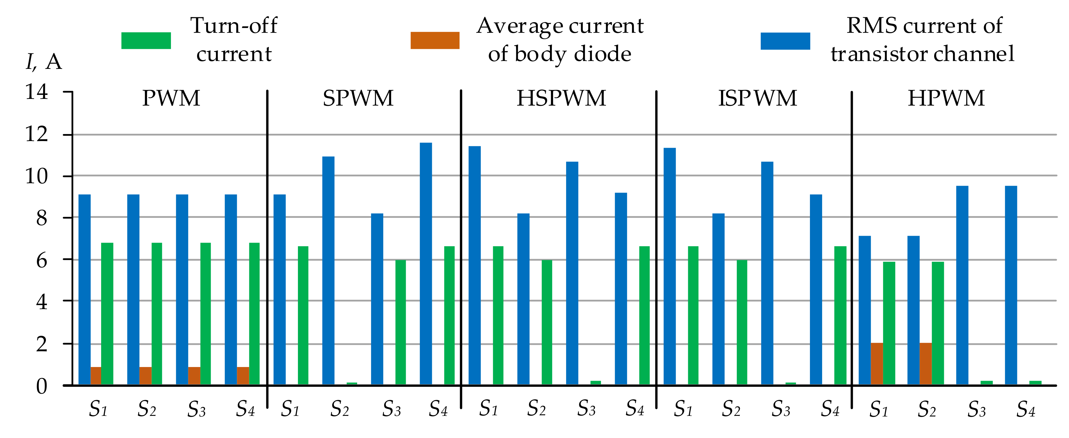
5.1. Comparison of Current Stresses

To benchmark the existing and the proposed PWM methods, current stresses have to be analyzed. Three main current stresses were considered:
  • Turn-off current—as it defines the switching losses of the switches in the case of PWM of the SRC;
  • The RMS current of the MOSFET channel (considering current flowing only when a switch is turned on)—as it influences the conduction losses of the switches;
  • The average current of the body diode (considering negative current flowing when a MOSFET is turned off)—as it could increase the conduction losses in the switches significantly.
The current stress and losses of the output side components are virtually the same for all the PWM methods and thus are excluded from the benchmarking.
A diagram of the transistor channel RMS currents (blue), the average current of body diodes (orange), and the transistor turn-off currents (green) is plotted in Figure 5 for the described PWM methods. The numerical values are provided for the input power (P) of 200 W at the input voltage of 50 V. It can be seen from the diagram that the conventional PWM method has the highest value of the transistor turn-off currents, and a relatively high average current of the body diodes, which are equal for all the switches. Two body diodes have a high value of the average current in the case of the HPWM method. However, the other two diodes have zero average currents. The overall current stress of the body diodes in the case of the HPWM method is lower than that of the conventional PWM method. Moreover, the HPWM method achieves nearly zero switching currents of two transistors. All the shifted PWM methods target the reduction in the conduction losses, as they provide nearly zero average currents of the body diodes. Even though the current stresses redistribute among the switches differently, their cumulative values are the same for the SPWM, HSPWM, and ISPWM methods. Hence, the main practical difference is in avoiding parasitic oscillations that can occur in the SRC during freewheeling or zero states in the front-end inverter.

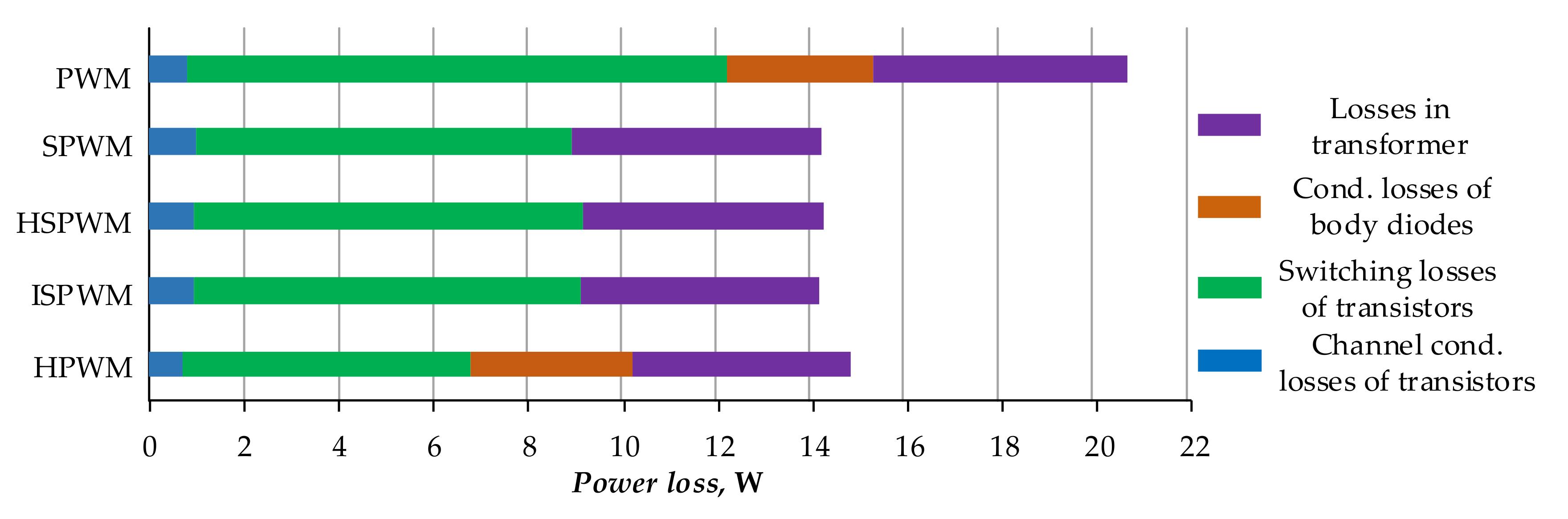
5.2. Comparison of Power Losses in the SRC Controlled by PWM Methods

The calculation of losses in MOSFETs is based on the methodology in [31]. It uses the most conventional approach based on the datasheet parameters, such as parasitic output capacitance, fall and rise times, gate resistance and capacitance. The conduction losses were calculated using conventional methods, where a turned-on MOSFET is replaced with a resistor imitating its drain-to-source resistance in the on-state, while a diode is considered as a series connection of voltage source and a resistance imitating the forward voltage drop and the differential resistance of a diode. The main datasheet parameters used for the calculation of losses are listed in Table 1 and Table 2.
Power losses of the converter are shown in Figure 6 for the described control methods. The bar diagram includes conduction losses of transistors (blue), switching losses of transistors (green), conduction losses of body diodes (orange), and conduction losses of the transformer (magenta) for different PWM methods. These losses are dominant in the given case. Losses in the output side components are not listed as they are virtually the same for all PWM methods, and thus, they are not presented for brevity. Power losses in the rectifier diodes equal about 3 W in each method, which depend directly on the output current, and thus, are virtually the same for all considered methods in the lossless system. Therefore, it was omitted from the comparison of the PWM methods. All PWM methods feature nearly equal but low conduction losses. It is the result of using high-performance MOSFETs with low on-state resistance. The conventional PWM method has the highest switching losses because all four transistors are turned off at a high current. In comparison, the use of the HPWM method results in decreased switching losses in the transistors as only two switches are turned off at a high current. However, body diodes of the transistors S1 and S2 still suffer from high current stress and excessive conduction losses. This aspect would result in increased temperatures of these two transistors and should be taken into account during the thermal design of the converter.
As it was predicted for the shifted PWM methods above, the conduction losses of the transistors are represented by ohmic losses in the transistor channels. At the same time, body diodes experience negligible conduction losses. This reduction is achieved owing to the bypassing of the body diodes similar to the synchronous rectification concept. The idealized analysis of losses shows that the conventional SPWM provides lower losses than the other shifted PWM methods. However, the analysis ignores parasitic effects caused by the parasitic nonlinear output capacitance of the semiconductor devices, which can change distribution among losses in practice. In the case of the HSWPM and ISPWM, the twice higher switching frequency of the switch S1 does not generate much of the additional switching losses as its second turn-on and -off are performed under zero voltage and zero current conditions, respectively. Nevertheless, all shifted methods have higher total switching losses than those of the HPWM method.
Transformer losses are almost the same in all methods, which results from the similarity of the curve shapes of DC voltage gain in relation to the duty cycle DSD. However, the transformer losses of the SRC are the highest for the conventional PWM method due to the shortest duration of the current pulses in the transformer windings among all methods. In general, the shorter the current pulse, the higher the RMS current would be.
From the analysis of Figure 5 and Figure 6, it is evident that the front-end switches feature uneven power losses. As a result, the realization of the given SRC would require a custom approach to the thermal design. On the other hand, it could be assumed that the hottest transistor limits the output power if the custom thermal design is not practical. In this case, the three shifted PWM methods can deliver the highest power if all the transistors operate in the same cooling conditions.

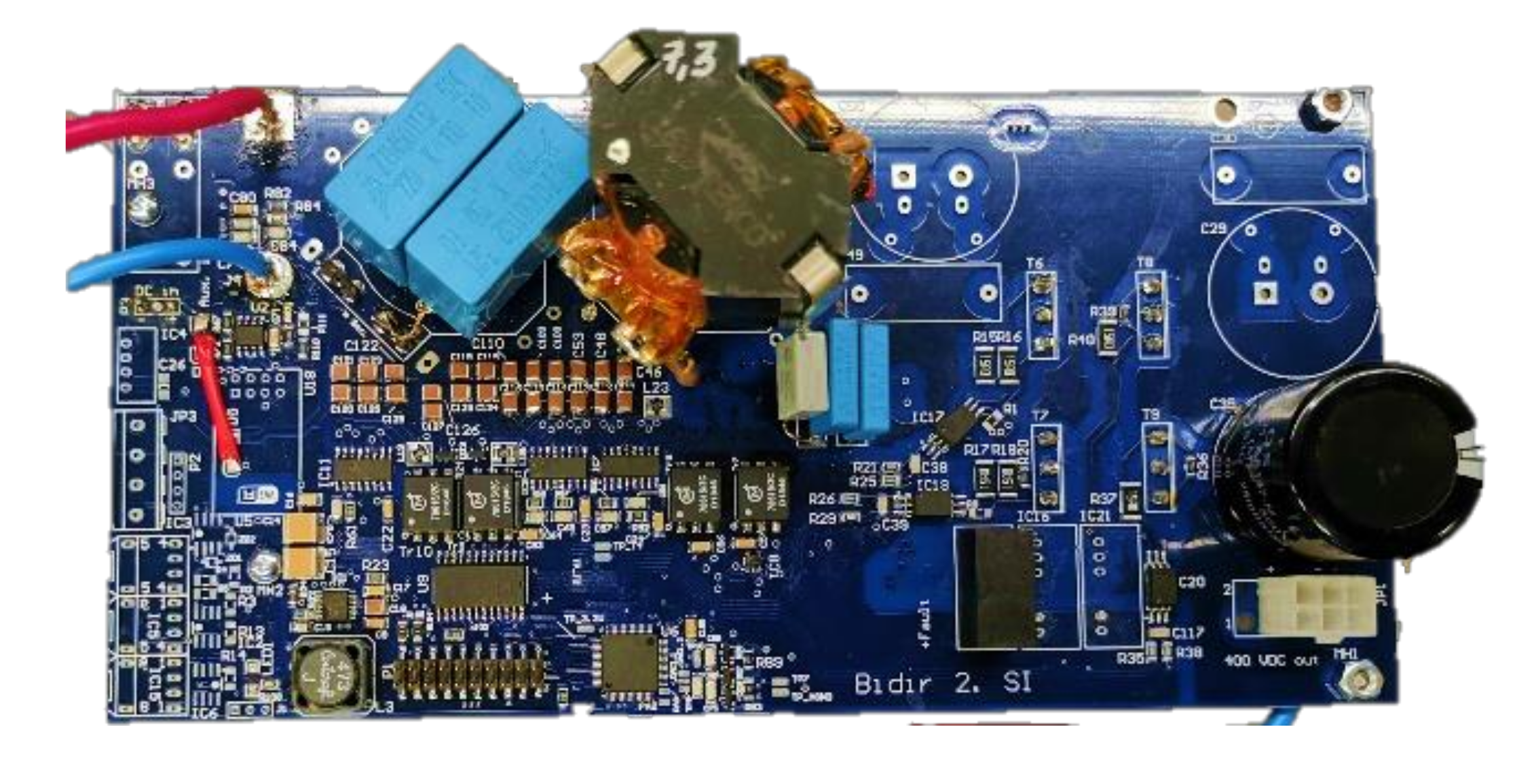
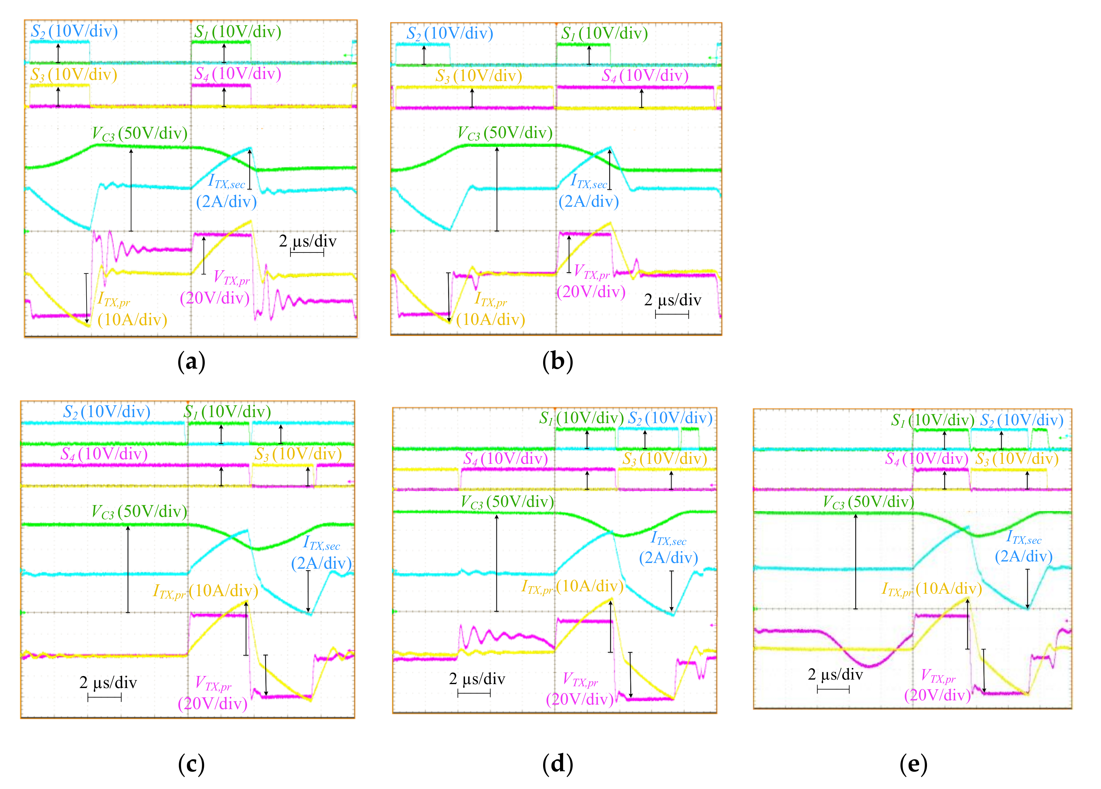
6. Experimental Results

A 200 W prototype of the SRC converter was built to verify the operation of the PWM control methods and compare experimental results with the theoretical analysis. The prototype is shown in Figure 7. The main components used in the prototype are listed in Table 1.

6.1. Steady-State Waveforms

Voltage and current waveforms of the SRC operating with PWM, HPWM, SPWM, HSPWM, and ISPWM control methods at Vin = 40 V, P = 200 W are shown in Figure 8. The following measurement equipment was used: oscilloscope DPO7254, differential voltage probes P5205A, current probes TCP0030A from Tektronix, Beaverton, OR, USA and precision power analyzer WT1800 from Yokogawa, Musashino, Tokyo, Japan.
Shapes of the transformer current waveforms (Figure 8) correspond to the theoretical curve of the resonant current in Figure 2 and Figure 4 for each PWM method. However, in the case of the conventional PWM method, the voltage shape of the transformer primary winding has a parasitic oscillation between the output capacitances of semiconductor devices and the leakage inductance (Figure 8a). For the HPWM and SPWM methods, the resonant current has a parasitic oscillation between the junction capacitances of the rectifier diodes and the leakage inductance (Figure 8b,c). The HSPWM method features parasitic oscillations after the transistor S3 is turned off and S4 is turned on after a short dead-time (Figure 8d). In the case of the ISPWM method, there are parasitic oscillations between the output capacitances of the semiconductor components and the magnetizing inductance of the transformer (Figure 8e). All the described parasitic oscillations occur when the resonant current drops to zero. These oscillations add extra conduction losses in the transformer and semiconductor devices.
It will be shown in the next subsection that the PWM methods feature nearly the same duty cycle DSD at the same DC voltage gain G. The magnitudes of the transformer current depend on the quality factor of the resonant tank, the turns ratio of the transformer, and the load power. Therefore, the magnitudes of the transformer current are practically the same for all modulation methods.

6.2. Normalized DC Voltage Gain
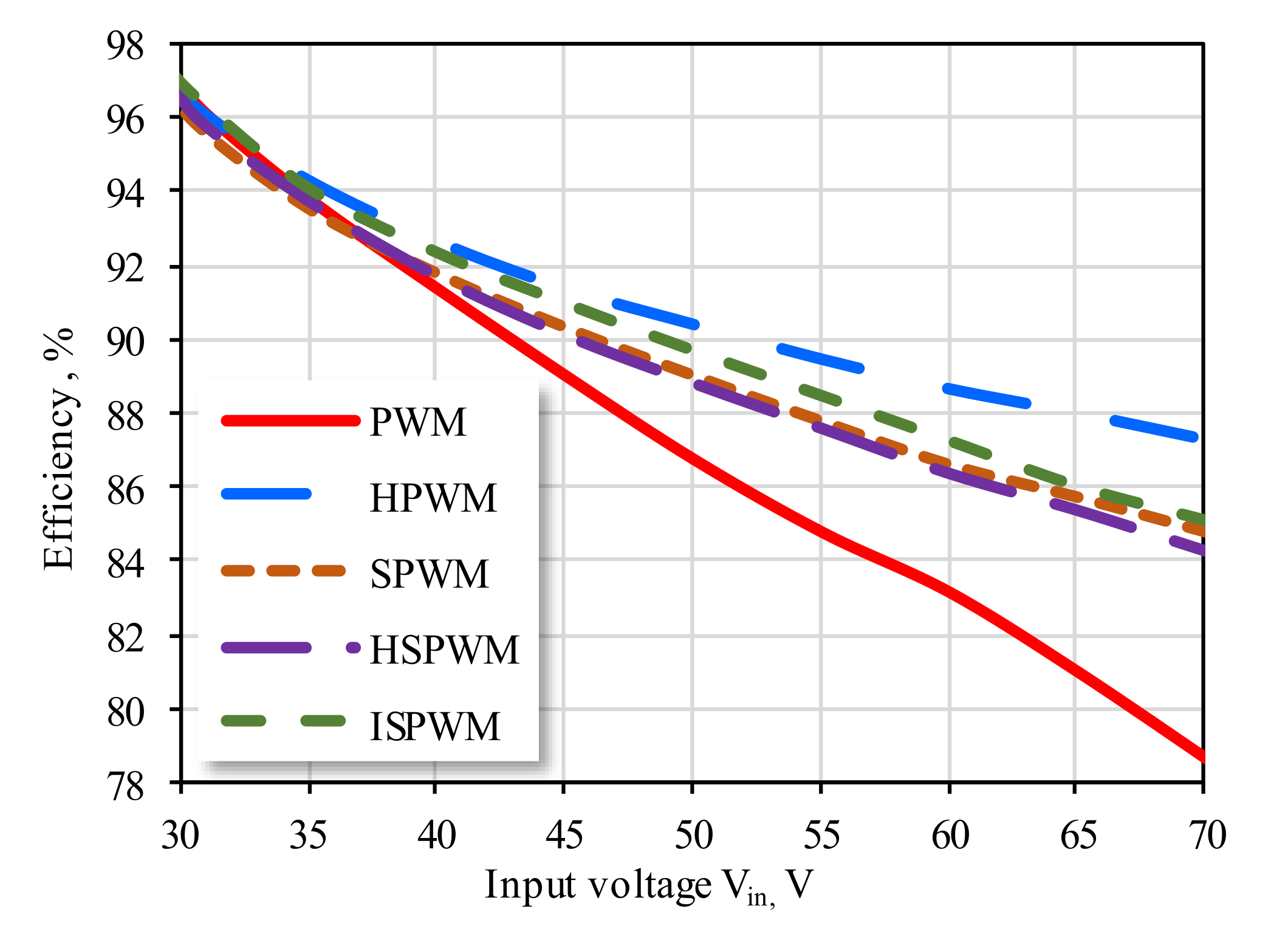
Normalized DC voltage gain of the case study converter as a function of the duty cycle is plotted in Figure 9 at different operating powers p, using Equations (18) and (30) and the numerical analysis based on (21)–(27). It is compared to the experimental results for the input voltage range from 30 to 70 V. The figure shows that the voltage gain curves are almost identical for all the compared methods. It is worth mentioning that each PWM method features a dead control zone where the DC voltage gain G is weakly dependent on the duty cycle DSD. The five methods considered in Figure 9 show good agreement between the theoretical and experimental results. Small differences occur outside the target regulation range and are mostly associated with the assumptions of a lossless system and neglecting the influence of the magnetizing inductance during the analysis.

6.3. Efficiency

The efficiency of the prototype as a function of the input voltage is shown for different PWM methods at P = 200 W in Figure 10. It was observed that the conventional PWM has the highest power losses while the HPWM features the lowest losses among the compared methods.
The maximum efficiency of the prototype equals 97.25% at Vin = 30 V, P = 200 W, DDS = 0.5 for all modulation methods. At this point, there is virtually no voltage step-down performed, i.e., the maximum DC voltage gain is provided, and all semiconductor components are soft-switched. The switches are turned on and turned off at zero current, and the resonant current has a purely sinusoidal shape. However, the duty cycle DSD has to decrease with an increase in the input voltage, which results in increased power losses. The difference in the efficiency between the PWM methods is mostly associated with the switching losses, the conduction losses in the body diodes of the MOSFETs, and additional losses from the parasitic oscillations.
When using PWM control methods, all transistors are turned off at high current, which results in the dominance of the switching losses. The parasitic oscillations add extra losses, as was predicted above. The use of the HPWM method results in decreased switching losses in the transistors S3 and S4. In addition, these transistors are turned on when conducting the negative current. As a result, their body diodes do not conduct any current and, consequently, their conduction losses are minimized. Contrary to that, the body diodes of the transistors S1 and S2 still suffer from high current stress and excessive conduction losses.
Even though all the body diodes have nearly zero conduction losses in the case of the shifted PWM methods, the cumulative switching losses of the transistors are higher in comparison with the HPWM method. As a result, their efficiency is lower than that of the HPWM method. It should be noted that the SPWM and HSPWM methods feature high-frequency parasitic oscillations between the leakage inductance of the transformer and the parasitic capacitances of the semiconductor components. These high-frequency parasitic oscillations increase power losses in the converter components, especially in the transformer winding due to increased influence of skin and proximity effects as high frequencies. On the other hand, parasitic oscillations with the transformer magnetizing inductance were observed at a much lower frequency in the case of ISPWM, which causes lower additional losses and higher efficiency compared to those of the SPWM and HSPWM methods. These additional power losses result in the superiority of the HPWM method over the three shifted PWM methods, which is different from the performance prediction in Figure 6 that ignores these parasitic effects.

7. Conclusions

In low-cost implementations of the series resonant DC–DC converter, the use of the transformer leakage inductance in the resonant tank is required. As a result, operation with a low quality factor of the resonant tank is inevitable. On the other hand, this enables converter operation at a fixed switching frequency. This study targets voltage buck functionality in high step-up SRC using PWM. The focus is on the PWM methods that can be used for both full- and half-bridge converters.
Prior to this study, there were only two PWM methods proposed for this application. This paper introduces a generalized methodology that yields precise estimations of the DC voltage gain for the PWM methods. The two existing PWM methods were analyzed to identify their main drawbacks, such as high switching losses, parasitic oscillations, and excessive conduction losses in MOSFET body diodes. The hybrid PWM method was proposed to reduce switching losses of the conventional PWM method. Improved and hybrid shifted PWM methods were proposed to minimize parasitic oscillations generating additional losses in the case of the conventional shifted PWM method.
The hybrid PWM method provides up to 9% efficiency improvement over the conventional PWM method. On the other hand, the losses are distributed among the switches unevenly in the case of the hybrid PWM, while the conventional PWM has evenly distributed losses. This should be taken into account during the SRC thermal design. The efficiency difference between the shifted PWM methods is much smaller. The improved shifted PWM can provide over 1% improvement over the other shifted PWM methods. The main efficiency improvement is related to avoiding high-frequency parasitic oscillations between the magnetic components and the parasitic capacitances of the semiconductors. Instead, the improved shifted PWM operates with the parasitic oscillations at a considerably reduced frequency related to the magnetizing inductance, which results in lower overall losses. The hybrid PWM provides the best efficiency among other PWM methods, which is up to 3% higher than that of the improved shifted PWM method. It has to be noted that only conventional PWM features equal distribution of power losses among the switches.
The main drawback of the SRC with a low quality factor is in operation at low duty cycle values, resulting in high RMS current stress of the components, which deteriorates the efficiency of the converter. Nevertheless, two directions of efficiency improvement could be suggested for future research: analysis of soft-switching implementation possibilities to reduce the switching losses that are dominant for all PWM methods, and the optimization of the transformer design to reduce the equivalent series resistance of the windings that causes high conduction losses while keeping relatively high leakage inductance of the transformer.

Author Contributions

Conceptualization, V.S. and A.C.; methodology, V.S.; software, V.S.; validation, A.C. and V.S.; formal analysis, A.C. and V.S.; investigation, V.S.; resources, D.V.; data curation, A.C.; writing—original draft preparation, A.C. and V.S.; writing—review and editing, A.C. and D.V.; visualization, A.C. and V.S.; supervision, A.C.; project administration, A.C.; funding acquisition, A.C. All authors have read and agreed to the published version of the manuscript.

Funding

This research was supported in part by the Estonian Research Council grant PSG206, and in part by the Estonian Centre of Excellence in Zero Energy and Resource Efficient Smart Buildings and Districts, ZEBE, grant 2014-2020.4.01.15-0016 funded by the European Regional Development Fund.

Conflicts of Interest

The authors declare no conflict of interest.

References

  1. Rodriguez-Otero, M.A.; O’Neill-Carrillo, E. Efficient Home Appliances for a Future DC Residence. In Proceedings of the 2008 IEEE Energy 2030 Conference, Atlanta, GA, USA, 17–18 November 2008. [Google Scholar] [CrossRef]
  2. Li, W.; Mou, X.; Zhou, Y.; Marnay, C. On Voltage Standards for DC Home Microgrids Energized by Distributed Sources. In Proceedings of the 7th International Power Electronics and Motion Control Conference, Harbin, China, 2–5 June 2012. [Google Scholar] [CrossRef]
  3. Anand, S.; Fernandes, B.G. Optimal Voltage Level for DC Microgrids. In Proceedings of the IECON 2010—36th Annual Conference on IEEE Industrial Electronics Society, Glendale, AZ, USA, 7–10 November 2010. [Google Scholar] [CrossRef]
  4. Dragicevic, T.; Vasquez, J.C.; Guerrero, J.M.; Skrlec, D. Advanced LVDC Electrical Power Architectures and Microgrids: A Step toward a New Generation of Power Distribution Networks. IEEE Electr. Mag. 2014, 2, 54–65. [Google Scholar] [CrossRef] [Green Version]
  5. Rodriguez-Diaz, E.; Chen, F.; Vasquez, J.C.; Guerrero, J.M.; Burgos, R.; Boroyevich, D. Voltage-Level Selection of Future Two-Level LVdc Distribution Grids: A Compromise Between Grid Compatibiliy, Safety, and Efficiency. IEEE Electrif. Mag. 2016, 4, 20–28. [Google Scholar] [CrossRef] [Green Version]
  6. Hannan, M.A.; Faisal, M.; Ker, P.J.; Mun, L.H.; Parvin, K.; Mahlia, T.M.I.; Blaabjerg, F. A Review of Internet of Energy Based Building Energy Management Systems: Issues and Recommendations. IEEE Access 2018, 6, 38997–39014. [Google Scholar] [CrossRef]
  7. Yuan, B.; Yang, X.; Li, D.; Wang, Z. A New Architecture for High Efficiency Maximum Power Point Tracking in Grid-Connected Photovoltaic System. In Proceedings of the 2009 IEEE 6th International Power Electronics and Motion Control Conference, Wuhan, China, 17–20 May 2009. [Google Scholar] [CrossRef]
  8. Carrasco, J.M.; Franquelo, L.G.; Bialasiewicz, J.T.; Galvan, E.; PortilloGuisado, R.C.; Prats, M.A.M.; Leon, J.I.; Moreno-Alfonso, N. Power-Electronic Systems for the Grid Integration of Renewable Energy Sources: A Survey. IEEE Trans. Ind. Electron. 2006, 53, 1002–1016. [Google Scholar] [CrossRef]
  9. Cacciato, M.; Consoli, A.; Attanasio, R.; Gennaro, F. Soft-Switching Converter With HF Transformer for Grid-Connected Photovoltaic Systems. IEEE Trans. Ind. Electron. 2010, 57, 1678–1686. [Google Scholar] [CrossRef]
  10. Min, B.D.; Lee, J.P.; Kim, J.H.; Kim, T.J.; Yoo, D.W.; Song, E.H. A New Topology With High Efficiency Throughout All Load Range for Photovoltaic PCS. IEEE Trans. Ind. Electron. 2009, 56, 4427–4435. [Google Scholar] [CrossRef]
  11. Vinnikov, D.; Chub, A.; Liivik, E.; Roasto, I. High-Performance Quasi-Z-Source Series Resonant DC–DC Converter for Photovoltaic Module-Level Power Electronics Applications. IEEE Trans. Power Electron. 2017, 32, 3634–3650. [Google Scholar] [CrossRef]
  12. Fu, M.; Fei, C.; Yang, Y.; Li, Q.; Lee, F.C. A GaN-Based DC–DC Module for Railway Applications: Design Consideration and High-Frequency Digital Control. IEEE Trans. Ind. Electron. 2020, 67, 1638–1647. [Google Scholar] [CrossRef]
  13. Chub, A.; Husev, O.; Blinov, A.; Vinnikov, D. Novel Isolated Power Conditioning Unit for Micro Wind Turbine Applications. IEEE Trans. Ind. Electron. 2017, 64, 5984–5993. [Google Scholar] [CrossRef]
  14. Krismer, F.; Biela, J.; Kolar, J.W. A Comparative Evaluation of Isolated Bi-Directional DC/DC Converters with Wide Input and Output Voltage Range. In Proceedings of the Fourtieth IAS Annual Meeting. Conference Record of the 2005 Industry Applications Conference, Kowloon, Hong Kong, China, 2–6 October 2005. [Google Scholar] [CrossRef]
  15. Dragicevic, T.; Lu, X.; Vasquez, J.C.; Guerrero, J.M. DC Microgrids—Part II: A Review of Power Architectures, Applications, and Standardization Issues. IEEE Trans. Power Electron. 2016, 31, 3528–3549. [Google Scholar] [CrossRef] [Green Version]
  16. Yu, S.-Y. A New Compact and High Efficiency Resonant Converter. In Proceedings of the 2016 IEEE Applied Power Electronics Conference and Exposition (APEC), Long Beach, CA, USA, 20–24 March 2016. [Google Scholar] [CrossRef]
  17. Yang, B.; Lee, F.C.; Zhang, A.J.; Huang, G. LLC Resonant Converter for Front End DC/DC Conversion. In Proceedings of the APEC. Seventeenth Annual IEEE Applied Power Electronics Conference and Exposition (Cat. No.02CH37335), Dallas, TX, USA, 10–14 March 2002. [Google Scholar] [CrossRef]
  18. Song, Z.; Gao, Y.; Shang, P. Parameter Design Method of a Series-Parallel Resonant Converter. In Proceedings of the 2018 IEEE 4th Information Technology and Mechatronics Engineering Conference (ITOEC), Chongqing, China, 14–16 December 2018. [Google Scholar] [CrossRef]
  19. Rahman, A.N.; Chiu, H.-J.; Hsieh, Y.-C. Design of Wide Input Voltage Range High Step-up DC-DC Converter Based on Secondary-Side Resonant Tank Full Bridge LLC. In Proceedings of the 2018 3rd International Conference on Intelligent Green Building and Smart Grid (IGBSG), Yi-Lan, Taiwan, 22–25 April 2018. [Google Scholar] [CrossRef]
  20. Chub, A.; Vinnikov, D.; Lai, J.-S. Input Voltage Range Extension Methods in the Series-Resonant DC-DC Converters. In Proceedings of the 2019 IEEE 15th Brazilian Power Electronics Conference and 5th IEEE Southern Power Electronics Conference (COBEP/SPEC), Santos, Brazil, 1–4 December 2019. [Google Scholar] [CrossRef]
  21. Yan, J.; Zhao, X.; Chen, C.; Lai, J.-S. Comparison of Secondary Topology of the LLC Converter for Photovoltaic Application. In Proceedings of the 2018 IEEE Energy Conversion Congress and Exposition (ECCE), Portland, OR, USA, 23–27 September 2018. [Google Scholar] [CrossRef]
  22. Vinnikov, D.; Chub, A.; Kosenko, R.; Zakis, J.; Liivik, E. Comparison of Performance of Phase-Shift and Asymmetrical Pulsewidth Modulation Techniques for the Novel Galvanically Isolated Buck–Boost DC–DC Converter for Photovoltaic Applications. IEEE J. Emerg. Sel. Top. Power Electron. 2017, 5, 624–637. [Google Scholar] [CrossRef]
  23. Vandelac, J.-P.; Ziogas, P.D. A DC to DC PWM Series Resonant Converter Operated at Resonant Frequency. IEEE Trans. Ind. Electron. 1988, 35, 451–460. [Google Scholar] [CrossRef]
  24. Moschopoulos, G.; Jain, P. A Series-Resonant DC/DC Converter with Asymmetrical PWM and Synchronous Rectification. In Proceedings of the 2000 IEEE 31st Annual Power Electronics Specialists Conference. Conference Proceedings (Cat. No.00CH37018), Galway, Ireland, 23–23 June 2000. [Google Scholar] [CrossRef]
  25. Sun, X.; Li, X.; Shen, Y.; Wang, B.; Guo, X. Dual-Bridge LLC Resonant Converter With Fixed-Frequency PWM Control for Wide Input Applications. IEEE Trans. Power Electron. 2017, 32, 69–80. [Google Scholar] [CrossRef]
  26. Luan, B.-Y.; Hu, S.; Zhang, Y.-F.; Li, X. Steady-State Analysis of a Series Resonant Converter with Modified PWM Control. In Proceedings of the 2017 12th IEEE Conference on Industrial Electronics and Applications (ICIEA), Siem Reap, Cambodia, 18–20 June 2017. [Google Scholar] [CrossRef]
  27. Singh, Y.V.; Viswanathan, K.; Naik, R.; Sabate, J.A.; Lai, R. Analysis and Control of Phase-Shifted Series Resonant Converter Operating in Discontinuous Mode. In Proceedings of the 2013 Twenty-Eighth Annual IEEE Applied Power Electronics Conference and Exposition (APEC), Long Beach, CA, USA, 17–21 March 2013. [Google Scholar] [CrossRef]
  28. Kim, E.H.; Kwon, B.H. Zero-Voltage- and Zero-Current-Switching Full-Bridge Converter With Secondary Resonance. IEEE Trans. Ind. Electron. 2010, 57, 1017–1025. [Google Scholar] [CrossRef]
  29. Pahlevani, M.; Pan, S.; Jain, P. A Hybrid Phase-Shift Modulation Technique for DC/DC Converters With a Wide Range of Operating Conditions. IEEE Trans. Ind. Electron. 2016, 63, 7498–7510. [Google Scholar] [CrossRef]
  30. Vinnikov, D.; Chub, A.; Korkh, O.; Malinowski, M. Fault-Tolerant Bidirectional Series Resonant DC-DC Converter with Minimum Number of Components. In Proceedings of the 2019 IEEE Energy Conversion Congress and Exposition (ECCE), Baltimore, MD, USA, September 29–3 October 2019. [Google Scholar] [CrossRef]
  31. Graovac, D.; Purschel, M.; Kiep, A. “MOSFET Power Losses Calculation Using the Data-Sheet Parameters”, Infineon Application Note, July 2006. Available online: https://application-notes.digchip.com/070/70-41484.pdf (accessed on 21 June 2020).
Figure 1. Case study series resonant converter.
Energies 13 04569 g001
Figure 2. Series resonant DC–DC converter (SRC) operation with the conventional pulse-width modulation (PWM) [23] (a) and shifted pulse-width modulation (SPWM) [26] (b).
Energies 13 04569 g002
Figure 3. Equivalent circuit describing the parasitic oscillations in the SRC for the SPWM method.
Energies 13 04569 g003
Figure 4. SRC operation with the proposed HSPWM (a), ISPWN (b) and HPWM (c) methods.
Energies 13 04569 g004
Figure 5. Diagram of current stresses of the switches at Vin = 50 V, P= 200 W for different PWM methods.
Energies 13 04569 g005
Figure 6. Diagram of the power losses in the SRC at Vin = 50 V, P = 200 W for different PWM methods.
Energies 13 04569 g006
Figure 7. Prototype of the SRC converter.
Energies 13 04569 g007
Figure 8. Experimental steady-state waveforms of the SRC operating at Vin = 40 V, P = 200 W for PWM (a), HPWM (b), SPWM (c), HSPWM (d), and ISPWM (e) methods.
Energies 13 04569 g008
Figure 9. Normalized voltage gain of the case study SRC for PWM (a), HPWM (b), SPWM (c), HSPWM (d), and ISPWM (e) control methods.
Energies 13 04569 g009
Figure 10. The measured efficiency of the case study SRC for different PWM methods at P = 200 W.
Energies 13 04569 g010
Table 1. General specifications of the converter.
Operating Parameters
Input Voltage Range, Vin30–70 V
Output Voltage, Vout350 V
Switching Frequency, fSW100 kHz
Operating Power Range50–200 W
Components
S1–S4On Semiconductor FDMS 86180
D1, D2CREE C3D02060E
C1, C5150 µF
C252.8 µF
C3, C443 nF
Llk28 µH
Lm1 mH
n6.3
Table 2. General specifications of MOSFET FDMS86180, ON Semiconductor (Phoenix, AZ, USA).
ON-State Resistance2.4 mΩ
Output Capacitor3730 pF
Rise Time12 ns
Fall Time7 ns
Total Gate Charge60 nC
Gate-Source Voltage10 V
Total Gate Resistance3.5 Ω
Gate-Drain Capacitance (VDS = 0 V)500 pF
Body Diode Forward Voltage0.8 V
Body Diode on Resistance28 mΩ

