Article

Circuit-Based Electrothermal Simulation of Multicellular SiC Power MOSFETs Using FANTASTIC

by
Vincenzo d’Alessandro
1,*,
Lorenzo Codecasa
2,
Antonio Pio Catalano
1 and
Ciro Scognamillo
1
1
Department of Electrical Engineering and Information Technology, University Federico II, 80125 Naples, Italy
2
Department of Electronics, Information and Bioengineering, Politecnico di Milano, 20133 Milan, Italy
*
Author to whom correspondence should be addressed.
Energies 2020, 13(17), 4563; https://doi.org/10.3390/en13174563
Submission received: 26 June 2020 / Revised: 29 August 2020 / Accepted: 30 August 2020 / Published: 3 September 2020
(This article belongs to the Special Issue Latest Advances in Electrothermal Models)

Abstract

:
This paper discusses the benefits of an advanced highly-efficient approach to static and dynamic electrothermal simulations of multicellular silicon carbide (SiC) power MOSFETs. The strategy is based on a fully circuital representation of the device, which is discretized into an assigned number of individual cells, high enough to analyze temperature and current nonuniformities over the active area. The cells are described with subcircuits implementing a simple transistor model that accounts for the utmost influence of the traps at the SiC/SiO2 interface. The power-temperature feedback is emulated with an equivalent network corresponding to a compact thermal model automatically generated by the FANTASTIC tool from an accurate 3D mesh of the component under test. The resulting macrocircuit can be solved by any SPICE-like simulation program with low computational burden and rare occurrence of convergence issues.

1. Introduction

Silicon carbide (SiC) power devices are promising candidates for energy distribution, as well as for automotive, aircraft, and spacecraft applications, by virtue of their inherent features like high breakdown voltage, low on-state resistance, and excellent high-temperature capability [1].
Unfortunately, such devices often operate under critical conditions with a large amount of heat generation, which may lead to reliability degradation or even to an irreversible device failure in harsh cases. As a consequence, reliable simulation tools accounting for electrothermal (ET) effects are highly desired to define the thermal dissipation constraints and optimize the design of the transistor layout and/or of the cooling system. Such tools must be suited to describe temperature and current nonuniformities, which are often responsible for the safe operating area shrinking of transistors with a multicellular pattern. However, conceiving and developing a viable simulation strategy are challenging tasks due to multiple reasons. Fully numerical 3D ET analyses with device simulators concurrently solving the semiconductor and heat transfer equations are computationally unfeasible. Commonly-adopted approaches rely (i) on the interaction between a circuit simulation program and a 3D thermal-only numerical solver in a relaxation procedure [2,3], or (ii) on the extension of a finite-volume/-element software package to account for the electrical behavior of the transistor with simplified models [4,5]. However, for the specific case of SiC power devices, results can be trustworthy only by using models that accurately describe the key physical parameters and their non-intuitive temperature dependences, which are rather different compared to the traditional silicon (Si) counterparts. In addition, regardless of the technology, the pre-processing geometry/mesh construction within the environment of the thermal solver is onerous and troublesome. Lastly, these approaches are very resource-hungry and prone to convergence failures, especially if dynamic simulations under critical conditions have to be performed.
In this paper, an innovative circuit-based ET simulation approach is proposed for multicellular SiC power MOSFETs, with the ambition of optimizing the trade-off between computational efficiency and accuracy. The strategy is articulated as follows: (i) the device is discretized into an assigned number N of individual cells (each associated to an independent heat source) described with a simple, yet accurate model accounting for the relevant influence of SiC/SiO2 interface traps; (ii) the cell model is implemented with a SPICE-compatible subcircuit; (iii) an exceptionally accurate 3D finite-element method (FEM) description of the device is effortlessly obtained through a commercial solver aided by an in-house routine; (iv) the FANTASTIC code [6] is invoked, which automatically generates a dynamic compact thermal model (DCTM) of the device from the FEM representation, and thus builds an electrical network emulating the power-temperature feedback; (v) such a network is enriched with suitable voltage sources to account for nonlinear thermal effects, and the resulting circuit is referred to as thermal feedback block; (vi) a purely-electrical macrocircuit describing the whole ET behavior of the power device is constructed by connecting the N cell subcircuits to the thermal feedback block; (vii) the macrocircuit can be solved by any commercial circuit simulator in very short times and with unlikely occurrence of convergence problems. A multicellular 4H-SiC power MOSFET soldered on a direct bonded copper (DBC) substrate and operated under dc, short-circuit (SC), and unclamped inductive switching (UIS) conditions is considered as a case study.
This work extends the preliminary contribution [7], where a fully circuital representation of the SiC power MOSFET was obtained and solved with a similar approach. However, the generation of the thermal feedback block, based on Foster networks, was carried out in a long pre-processing stage involving N 3D FEM transient simulations, as well as a procedure to determine the proper number of RC pairs of each network and identify their values; in addition, the thermal interactions among horizontally-far cells were either coarsely described or even disregarded.
The remainder of the paper is articulated as follows. In Section 2, the device selected to test the approach and the experimental setup are described. Section 3 offers details concerning the transistor model used for the elementary cells. Section 4 probes into the ET simulation approach. Results are reported and discussed in Section 5. Conclusions are then drawn in Section 6.

2. Device under Test and Experimental Setup

The whole analysis was performed on the CREE 4H-SiC vertical double-diffused MOSFET (VDMOS) denoted as CPMF-1200-S080B, rated 1200 V, 50 A, 80 mΩ, and targeted at solar inverters, high-voltage dc–dc converters, and motor drives. A top-view picture of the device under test (DUT) is given in Figure 1; indicated are the gate pad, the two source pads, and the gate interconnect tracks. The DUT presents a 4.08 × 4.08 mm2 die area and a 3.46 × 3.46 mm2 active area (there is a peripheral inactive region), the effective portion of which contributing to the current capability amounts to about 10 mm2. The pattern is multicellular, with many thousands of body islands located in the N-drift region, within which there are source-body contacts surrounded by the polysilicon gate that lies beneath the source metal. The Ni/Ag drain contact is on the backside.
Isothermal measurements of IV transfer and output characteristics of the bare die were performed by means of an in-house 250 A-rated curve tracer suited to apply down to 1 µs-wide current pulses, the device baseplate being set to assigned temperatures TB through a thermochuck with 1 °C resolution. UIS experiments aimed at the evaluation of the breakdown voltage were carried out by a non-destructive custom tester [8]. The switching behavior was investigated by using a half-bridge converter board configured to perform a standard inductive load switching (ILS) test [9].

3. Transistor Model and Parameter Extraction Methodology

In the last decades, a noticeable effort has been made to develop models for SiC MOSFETs, a review of them being offered in [10]. Here we propose a slightly modified version of the behavioral model presented in [7,9] and used for ET simulations in [7,9,11]. Such a model, unlike those hitherto described in the literature, concurrently enjoys the following benefits: (i) it is simple, yet accurate enough, with a few parameters easy to extract; (ii) it can be implemented with a subcircuit compatible with any SPICE-like program; (iii) it includes all the key physical parameters and their specific temperature dependence up to very high temperatures; (iv) it also accounts for avalanche effects due to impact ionization (II); (v) the nonlinear nature of the intrinsic capacitances can be activated.

3.1. Transistor Model

The model is an enriched variant of the classic SPICE Level 1. In particular, the transistor is represented as the series of an “intrinsic” conventional MOSFET describing the channel behavior, and a resistance for the lowly-doped N-type epitaxial region, as depicted in Figure 2.
Let us consider the following nomenclature:
  • T [K] is the transistor temperature, assumed uniform in the regions impacting the device behavior.
  • T0 = 300 K is the reference temperature.
  • ΔT = TT0 [K] is the temperature rise over T0.
  • TB [K] the baseplate (and thermochuck) temperature.
  • VGS [V] is the gate-source voltage.
  • VDS [V] is the drain-source voltage.
  • ID [A] is the drain current.
  • Rdrift [Ω] is the bias- and temperature-dependent resistance of the N-type epitaxial drift region.
  • VDSch = VDSVdrift [V] is the VDS portion falling over the channel (Vdrift = Rdrift·ID).
  • VTH [V] is the temperature-dependent threshold voltage.
  • K [A/V2] is the temperature-dependent current factor.
The channel region is described with the Level 1 model. If VDSch is lower than the overdrive voltage VGSVTH, the DUT operates in triode mode, and the II-free drain current IDnoII is expressed as
I D n o I I = K [ 2 ( V G S V T H ) V D S c h V D S c h 2 ]
Conversely, if VDSchVGSVTH, then the DUT is driven into pinch-off, and
I D n o I I = K ( V G S V T H ) 2
The negative temperature coefficient of VTH is described through the following law:
V T H ( T ) = [ V T H ( T 0 ) V T H ] exp ( a V T H Δ T ) + V T H
such an exponential model being an improvement with respect to the simple linear relationship used in [7].
The current factor K depends upon T since the electron mobility in the channel is temperature-sensitive; similar to [7,9], such a dependence is taken into account through the power relationship
K ( T ) = K ( T 0 ) ( T T 0 ) m ( T )
where the exponent m(T) is
m ( T ) = a m + ( a m + b m ) [ 1 c m exp ( d m T T 0 ) ]
II effects are accounted for as follows [7,9]. The bias- and temperature-sensitive avalanche multiplication factor M (≥1) is given by [12]
M ( V D S , I D , T ) = 1 + m I I tan { f I ( I D ) π 2 [ V D S R I I I D B V D S ( T ) ] n I I }
where BVDS(T) is the temperature-dependent drain-source breakdown voltage, expressed as
B V D S ( T ) = B V D S ( T 0 ) exp ( α I I Δ T )
and fI(ID) is a nondimensional correction term to describe a potential II dependence on current (i.e., on biasing conditions), given by
f I ( I D ) = exp ( β I I I D )
Let us introduce the avalanche coefficient ξ = M − 1 (≥0). The II-affected drain current ID is evaluated as
I D = I D n o I I + I D I I = I D n o I I + ξ ( I l e a k + I D n o I I )
where IDII is the additional current component only dictated by II, and Ileak is a small leakage current.
The resistance Rdrift is expressed as the sum of (i) a bias- and temperature-dependent resistance RJFET to model the path composed by the accumulation and JFET regions, and (ii) a temperature-dependent resistance Repi for the epitaxial region beneath the JFET one [7,9]:
R d r i f t ( V G S , V d r i f t , T ) = R J F E T ( V G S , V d r i f t , T ) + R e p i ( T )
where
R J F E T ( V G S , V d r i f t , T ) = R J F E T ( T 0 ) ( T T 0 ) m R J F E T ( 1 1 + V 1 / V d r i f t ) ( V G S V 2 ) η R e p i ( T ) = R e p i ( T 0 ) ( T T 0 ) m R e p i
RJFET(T0) being the JFET resistance at T = T0, Vdrift » V1, and VGS = V2 (V1 and V2 are fitting parameters). This formulation improves the one reported in [7] in the high-current triode region and is derived on the basis of simple arguments. First, the resistance of the accumulation region reduces with gate voltage due to the increased concentration of the attracted electrons; second, under high Vdrift values, the high electric field occurring in the JFET region tends to saturate the electron velocity, thus degrading the mobility.
The dynamic transistor behavior is described by improving the Level 1 capacitance models; the nonlinear nature of CGD and CDS = CDB is accounted for with the following expressions [9]:
C G D ( V G D ) = ( C G D 0 C G D M I N ) [ 1 + 2 π arctan ( V G D V * ) ]
and
C D S ( V D S ) = 2 π C D S 0 [ π 2 + arctan ( V D S V * * ) ] + C D S M I N
while CGS was not modified [13].

3.2. Parameter Extraction Procedure

The threshold voltage VTH and the current factor K were extracted in a very wide TB range spanning from 300 to 500 K by resorting to the traditional quadratic extrapolation method [14,15] applied to IDVGS transfer characteristics measured under isothermal (pulsed) conditions at VDS = 20 V with the curve tracer mentioned in Section 2. Then the parameters in (3), (4), and (5) were calibrated so as to ensure the best matching between experimental data and the following relations:
V T H ( T B ) = [ V T H ( T 0 ) V T H ] exp [ a V T H ( T B T 0 ) ] + V T H
K ( T B ) = K ( T 0 ) ( T B T 0 ) m ( T B )
with
m ( T B ) = a m + ( a m + b m ) [ 1 c m exp ( d m T B T 0 ) ]
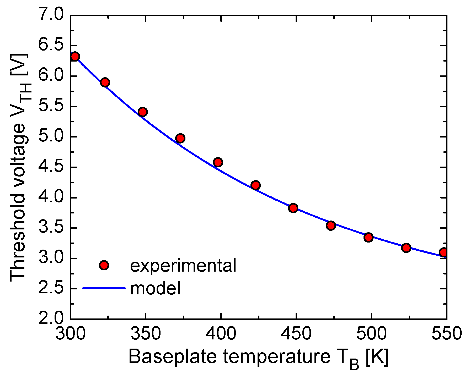
The comparison between the measured VTH and the optimized (14) is shown in Figure 3. It can be inferred that the DUT exhibits (i) a high VTH(T0) (≈6.4 V) and (ii) a high negative temperature coefficient of VTH(T) at low/medium TB compared to similarly-rated Si power MOSFETs. Both findings were attributed to the high density of SiC/SiO2 interface traps (quantum states originating from the thermal oxidation of the SiC surface); more specifically, (i) electrons are captured by traps and do not contribute to channel formation, thereby leading to a high threshold voltage VTH(T0), and (ii) VTH markedly reduces with temperature due to the concurrent effect of more broken bounds that release electrons, and of the emission of inversion electrons from the traps, the latter effect being almost absent in the Si counterparts [16,17,18]. It must be underlined that the strong negative temperature coefficient in turn contributes to a significant positive temperature coefficient of ID, which may exacerbate the ET feedback [19,20].
The comparison between the measured K and model (15) and (16) with tuned parameters is shown in Figure 4. The temperature sensitivity of K is only related to that of the channel electron mobility μn, which is due to the interplay between (i) the Coulomb scattering with the filled (charged) interface traps, leading to a positive temperature coefficient induced by the trap discharging (release of electrons) with increasing temperature, and (ii) the acoustic-phonon scattering favoring a negative coefficient, where (i) prevails at low temperatures and (ii) dominates at high temperatures [18,21,22,23]. This behavior is accurately described by the m model (16).
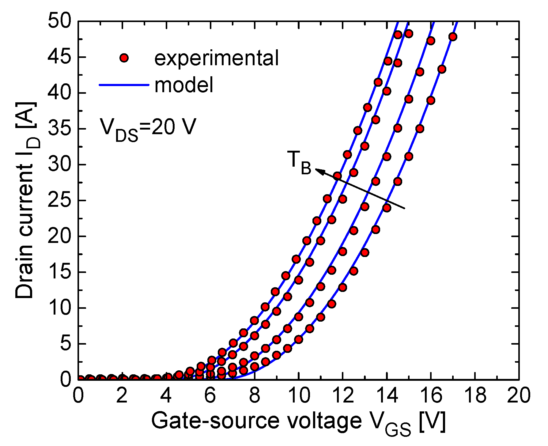
The accuracy of the parameter calibration for the VTH and K models is witnessed by the comparison reported in Figure 5 between (2) and the IDVGS transfer characteristics measured under isothermal conditions at VDS = 20 V and various TB values in a current range wherein the DUT operates in pinch-off (note that IDIDnoII). An inspection of the curves reveals the considerable positive temperature coefficient of ID within a wide range of currents.
The parameters of the drift resistance Rdrift in (10), (11) were optimized by comparing the IDVDS output characteristics at various VGS and different TB values in triode region with the model (1) applied to the scheme in Figure 2. Figure 6 reveals the accuracy of the extraction at TB = 303 K.
The parameters of the II model given by (6) with (7) and (8) were tailored on the basis of experimental data determined under UIS conditions, and 2D numerical simulations of the TB-dependent IDVDS avalanche curve at VGS = 0 V of an individual semi-cell of the DUT carried out with TCAD Sentaurus [24] (it must be remarked that the term “cell” here does not correspond to the discretization adopted in this work and identified by N, but it is one of the tens of thousands of identical blocks in which the effective active area of the MOSFET can be partitioned).
The parameters used in the expression of the capacitances CGD (12) and CDS (13) were calibrated to match the experimental gate and drain waveforms during an ILS turn-off and turn-on transient at different supply voltages.
All the optimized parameter values are reported in Table 1.

3.3. Impact of Interface Traps

The impact of the interface traps was investigated by resorting to the following strategy. The traps were virtually removed by (i) reducing VTH(T0) to 4 V, (ii) decreasing aVTH to 2 mK−1, (iii) multiplying the current factor K(T0) by 50 to annihilate the degradation of mobility μn(T0), and (iv) setting cm = 0 to eliminate the influence of Coulomb scattering on μn, which will thus exhibit a negative temperature coefficient over the whole temperature range. Figure 7 shows the comparison between the real 4H-SiC DUT and the ideal traps-free counterpart in terms of transfer characteristics at VDS = 20 V and various TB values. It can be inferred that:
  • differently from the DUT, which suffers from a marked positive temperature coefficient over the entire current range, the traps-free device is subject to a slight positive coefficient only at low drain current ID (<20 A), where the negative temperature coefficient of VTH prevails over the negative coefficient of μn, while beyond a zero-temperature coefficient region (also referred to as compensation region), the negative coefficient of μn dominates, and ID reduces with temperature.
  • the traps-free transistor benefits from a much higher current capability due to the lower VTH and the higher μn.
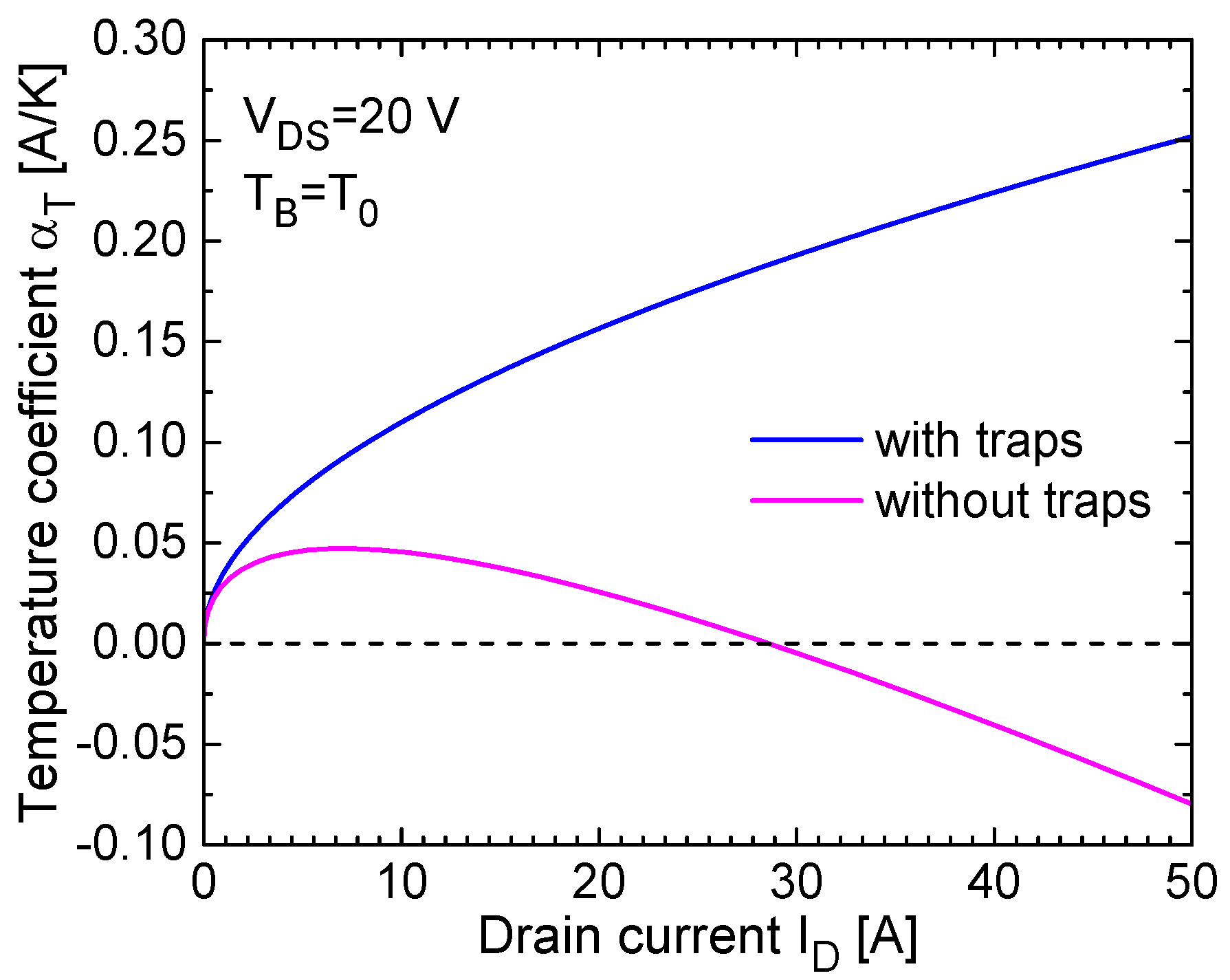
To further corroborate the above findings, Figure 8 reports the temperature coefficient of the drain current ID, given by [19,20,25]
α T = I D T | V D S
for the real DUT and its traps-free variant at reference temperature T0 and drain-source voltage VDS = 20 V; it is again witnessed that the traps at the SiC/SiO2 interface lead to a detrimental highly-positive αT within a broad range of currents.

4. Electrothermal Simulation Approach

We chose to resort to a circuit-based approach [7,11,26,27], which is a good trade-off between computational burden and accuracy. Such an approach makes use of the thermal equivalent of the Ohm’s law (TEOL) and can be summarized as follows.
  • The whole DUT is subdivided into an assigned number N of elementary cells, high enough to identify potentially-dangerous temperature gradients over the transistor active area, but not too high to prevent intolerably long CPU times or impossible memory storage. The individual cells are described with the model explained in Section 3, where the area-dependent parameters are properly scaled. For the simulation campaign reported in Section 5, all cells are assumed identical, although it is in principle possible to assign different parameter values to different cells to allow a statistical analysis of the influence of parameter fluctuations on the ET behavior of the component.
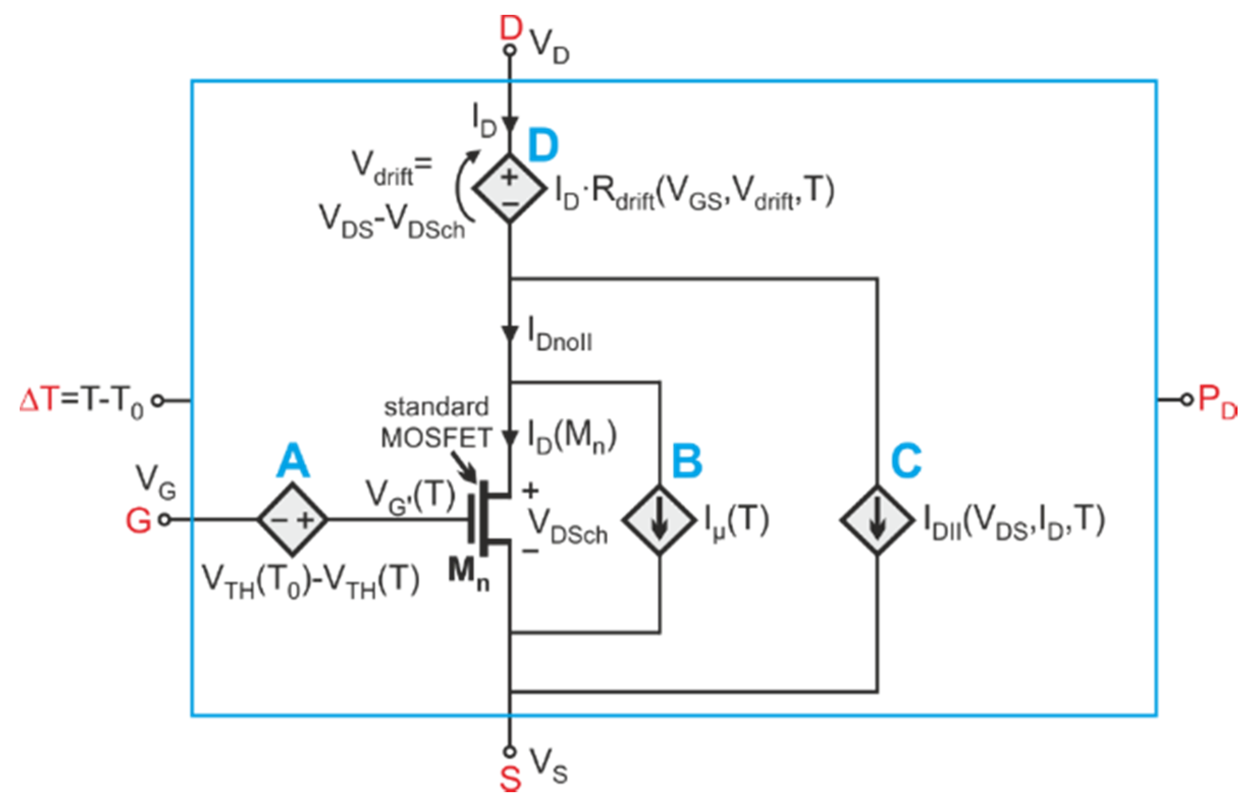
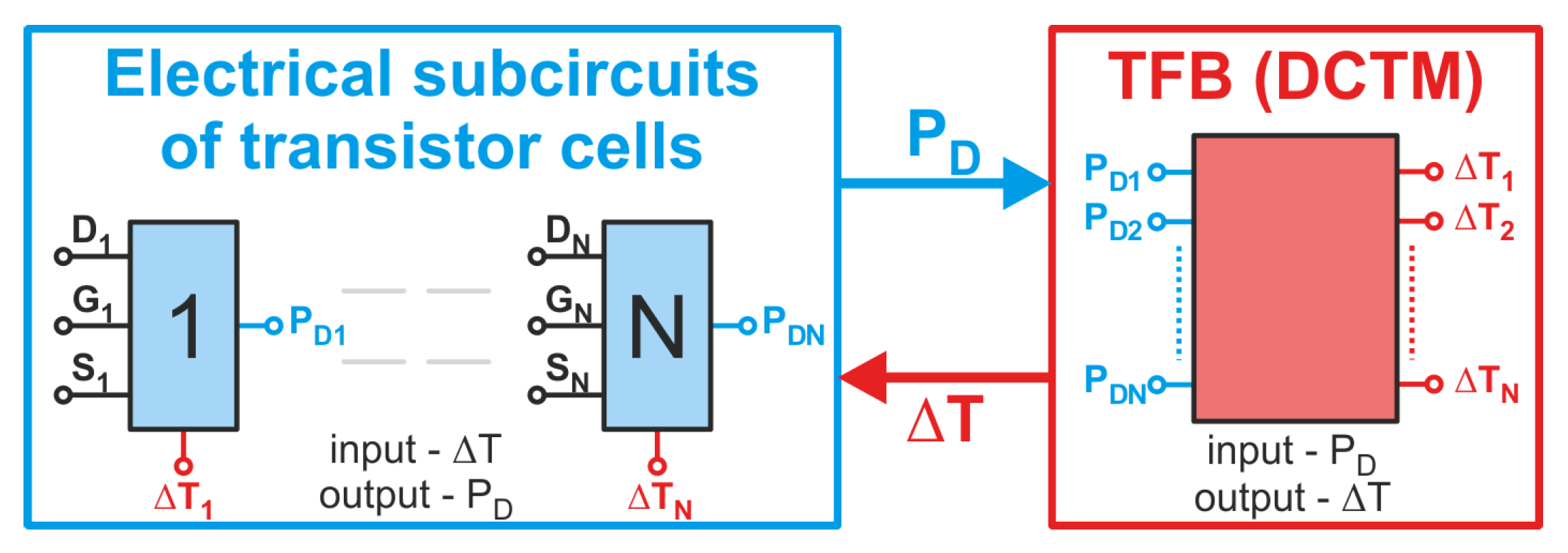
  • Each cell is represented with a SPICE-compatible subcircuit implementing the above model through a macromodeling technique. The subcircuit makes use of (i) a standard MOSFET at reference temperature T0 = 300 K as a “main” component to describe the channel region, and (ii) linear and nonlinear controlled sources to include all the model features that cannot be accounted for with the basic MOSFET, i.e., the temperature dependence of the threshold voltage VTH and of the current factor K, the bias- and temperature-dependent drift resistance Rdrift, as well as the bias- and temperature-dependent II mechanism. The TEOL is adopted, namely, the temperature rise over ambient ΔT = TT0 is actually a voltage, while the dissipated power PD is treated as a current; this allows (i) enabling the temperature sensitivity of the key physical parameters, and (ii) describing the power-temperature feedback with an electrical network. Besides the standard electrical terminals (gate, drain, source/body), the cell subcircuit is also equipped with an input node carrying the “voltage” ΔT (provided by the thermal feedback block introduced below) and with an output node offering the “current” PD (to be fed to the thermal feedback block).
  • The power-temperature feedback (i.e., the dynamic heat propagation within the structure) is described with a TEOL-based SPICE-compatible thermal feedback block, which is composed by resistances, capacitances, and controlled sources. The inputs of this block are the powers PD dissipated by the transistor cells (represented with currents), and the outcomes are the individual (nonlinear) temperature rises ΔT (emulated with voltages).
  • The thermal feedback block contains an equivalent thermal network (i.e., a purely-electrical circuit relying on the TEOL). The main contribution of the proposed approach is that this network is automatically constructed in the pre-processing stage by invoking the FANTASTIC tool [6] (Section 4.3). FANTASTIC receives as an input an accurate 3D FEM representation of the domain, i.e., a mesh with information about (i) the discretization into elementary cells (each corresponding to an individual heat source), (ii) material parameters, and (iii) boundary conditions, and then extracts a reduced-order model and the associated network without the need of user’s expertise and COMSOL simulations; only 16 min were needed for the case study. The equivalent network accurately accounts for the self-heating of each cell and for the mutual interactions among all cells and describes the linear thermal problem. However, nonlinear thermal effects can be significant if the DUT is simulated under harsh conditions entailing high temperatures. In order to tackle this issue, a properly-tuned Kirchhoff’s transformation [28] is used, which converts the linear temperature rises (ΔTlin) into their nonlinear counterparts (ΔT) through [29]
    Δ T = T 0 [ m k + ( 1 m k ) Δ T l i n + T 0 T 0 ] 1 1 m k T 0
    The calibration of the (positive) parameter mk will be detailed in Section 4.2. Nonlinear voltage-controlled voltage sources emulating (18) are applied to the N temperature rise nodes of the equivalent thermal network; the resulting circuit is referred to as a thermal feedback block. It is worth noting that the FANTASTIC-based approach improves the strategy exploited in [7,26], where the thermal feedback block was based on Foster networks extracted in a rather long pre-processing stage from N onerous transient COMSOL simulations of the DUT (performed by activating one heat source at a time), and the thermal coupling between horizontally-far heat sources was roughly described or even neglected.
  • The cell subcircuits are then connected to the thermal feedback block in a commercial circuit simulation tool (like PSPICE, LTSPICE, Eldo, ADS, SIMetrix); as a result, the whole domain under test, composed by the DUT soldered on a DBC substrate, is transformed into a purely-electrical macrocircuit, which suitably accounts for ET effects: the temperature, and thus the temperature-sensitive parameters, are allowed to vary during the simulation run. The solution of this macrocircuit under both static and dynamic conditions is demanded to the powerful and robust engine of the circuit simulation tool, with very low computational effort and minimized occurrence of convergence issues compared to other numerical methods.

4.1. SPICE Subcircuit and DUT Discretization into Cells

A sketch of the SPICE-compatible subcircuit for the transistor cell is represented in Figure 9, where the standard MOSFET instance at reference temperature T0 is indicated with Mn. The additional input node feeding the “voltage” ΔT and the output node providing the “current” PD are also represented.
The negative temperature coefficient of the threshold voltage VTH(T) described by (3) is accounted for by using the following approach. The voltage source A in series with the gate adds VTH(T0) − VTH(T) to VG, VTH(T) being given by (3), thus biasing Mn with VG’ = VG + [VTH(T0) − VTH(T)]; as a result, the effective overdrive voltage becomes
V G S V T H ( T 0 ) = V G S + [ V T H ( T 0 ) V T H ( T ) ] V T H ( T 0 ) = V G S V T H ( T )
and Mn conducts the current ID(Mn) given by
I D ( M n ) = K ( T 0 ) { 2 [ V G S V T H ( T ) ] V D S c h V D S c h 2 }                         V D S c h < V G S V T H ( T ) I D ( M n ) = K ( T 0 ) [ V G S V T H ( T ) ] 2                                                                                       V D S c h V G S V T H ( T )
The temperature dependence of the current factor K(T) expressed by (4) with (5) is emulated by using the current source B to derive the current
I μ = I D ( M n ) [ ( T T 0 ) m ( T ) 1 ]
Consequently, the II-unaffected current IDnoII is obtained as
I D n o I I = I D ( M n ) + I μ = I D ( M n ) + I D ( M n ) [ ( T T 0 ) m ( T ) 1 ] = I D ( M n ) ( T T 0 ) m ( T )
where m(T) is given by (5).
II effects are activated by adding an avalanche current IDII = ξ·(Ileak + IDnoII) to IDnoII through the current source C, ξ = M − 1 being bias- and temperature-dependent according to (6). Hence, the drain current ID flowing through the drift resistance Rdrift is given by (9).
The bias- and temperature-dependent Rdrift described by (10) with (11) is taken into account by making use of source D, which imposes the voltage drop
V d r i f t = I D R d r i f t ( V G S , V d r i f t , T ) .
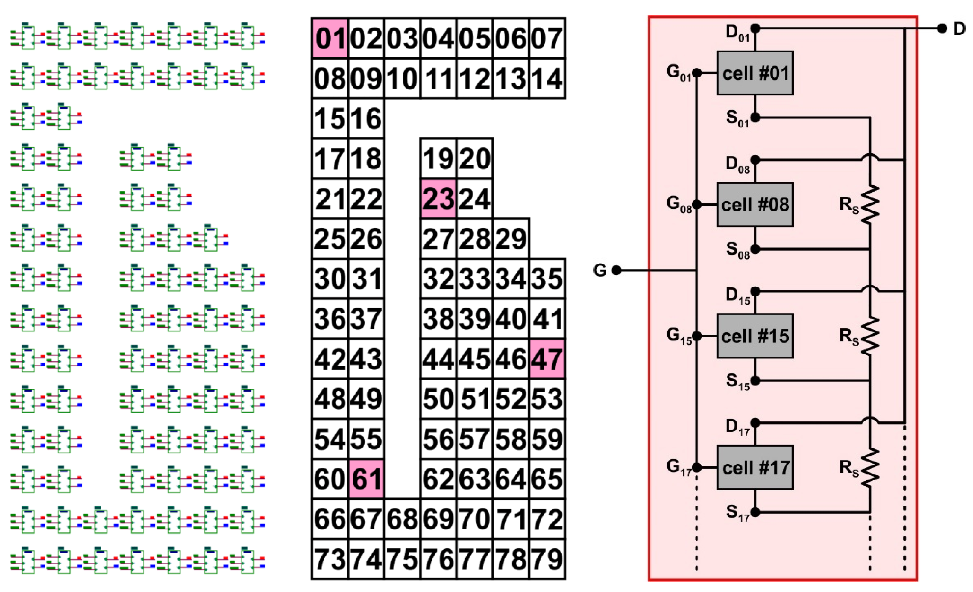
Only half of the DUT was represented and simulated by exploiting its inherent symmetry. The effective active region (≈5 mm2) was partitioned into N = 79 cells, each with a 250 × 250 µm2 area (the procedure leading to the choice of the N value will be detailed in Section 4.4). As a consequence, compared to those reported in Table 1, the values of the area-dependent parameters were scaled by dividing the current factor and the capacitances by 2 × N, and multiplying the resistances by 2 × N. The popular commercially-available OrCAD PSPICE [30] was chosen to perform circuit simulations. The main schematic (resembling the actual layout) is represented in Figure 10, along with the corresponding cell numbering and a detail of the connections between adjacent cells. The drain current of the resulting macrocircuit (an outcome of the ET simulation) has to be multiplied by 2.

4.2. FEM Representation of the Component under Test

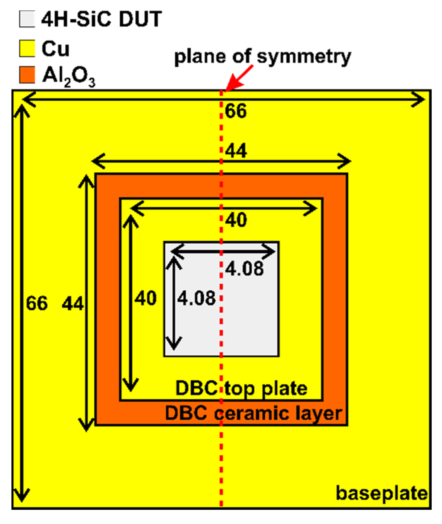
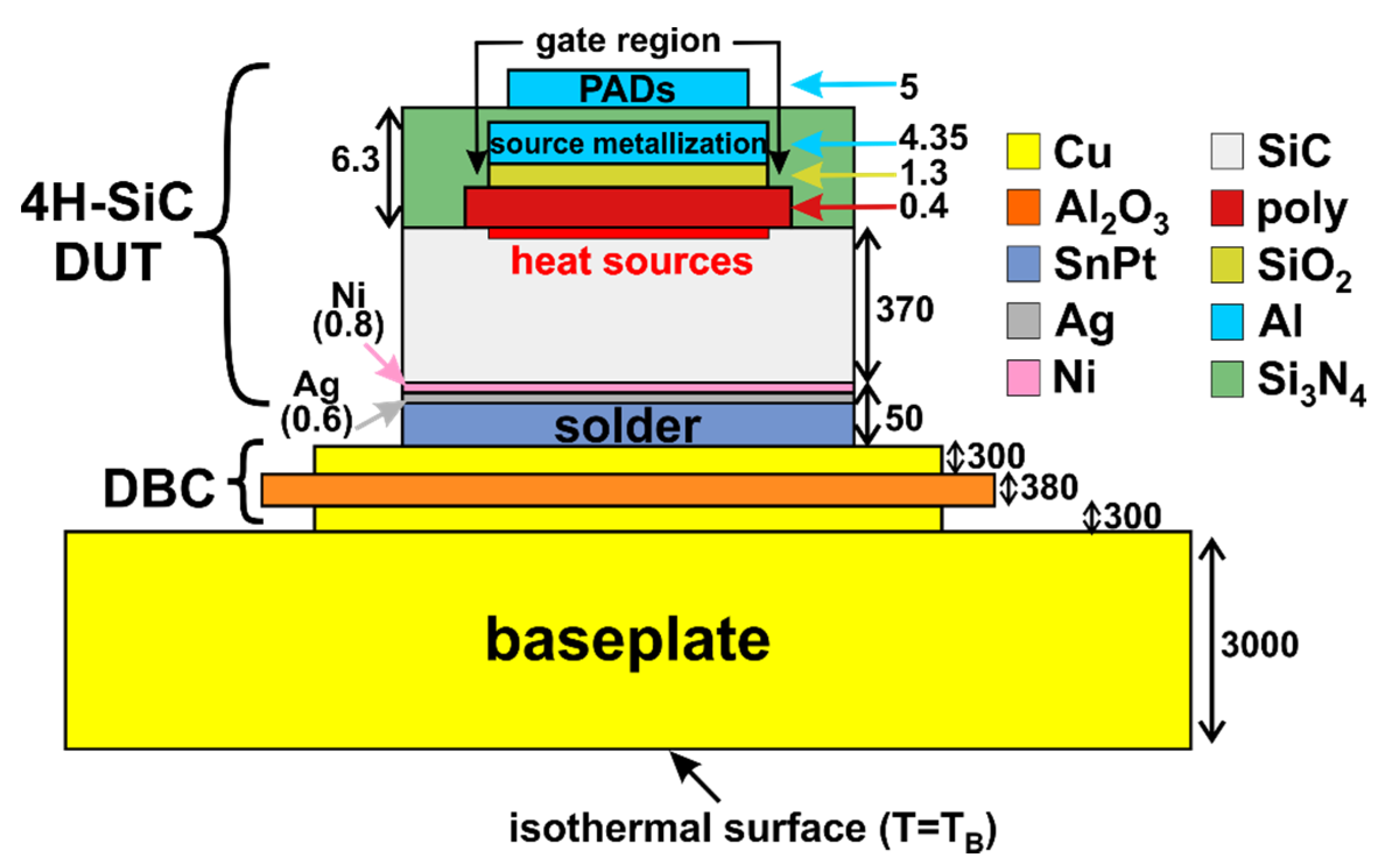
Exhaustive details on the geometry and materials of the DUT (the CPMF-1200-S080B VDMOS) were taken from the datasheet and from reports available on a reverse-engineering website. The DUT was assumed to be soldered on a DBC substrate by means of a 50 µm-thick tin-platinum alloy (SnPt) layer ensuring both mechanical joint and electrical connection with the drain [31]. Figure 11 and Figure 12 show the top view and cross-section of the assembly, which enjoys the same symmetry of the DUT. The soldering process can be automated by means of thin SnPt films, which are preformed and match the size of the die; in addition, alignment masks are typically exploited to ease their positioning. The DBC is composed by two copper (Cu) sheets (namely, bottom and top plates) with a ceramic layer placed in between them. Such a layer provides dielectric insulation to the assembly and is realized with alumina (Al2O3) for the proposed case study; however, alternative materials like silicon nitride (Si3N4) [32] and aluminum nitride (AlN) [33] are also adopted in the DBC manufacturing process. The drain contact of the DUT is soldered on the top plate, while the bottom plate ensures a good thermal interface with the 3 mm-thick Cu baseplate.
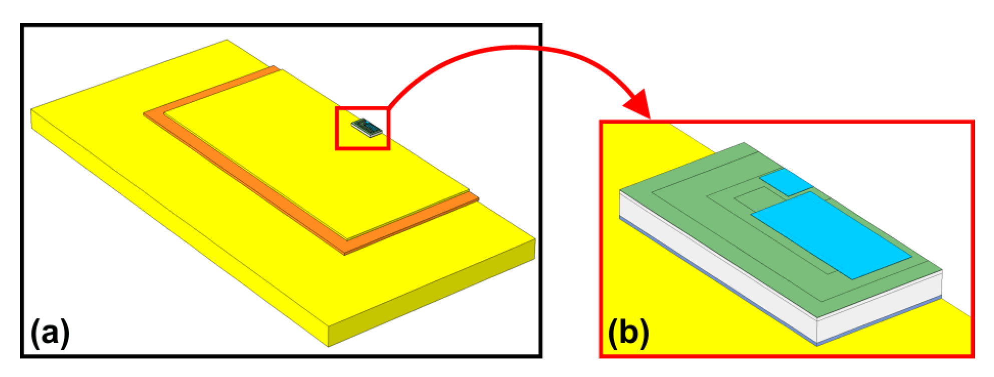
The 3D domain was represented in the environment of the commercial FEM-based COMSOL Multiphysics software package [34] by means of the in-house routine detailed in [35], which allows automatically building an extremely accurate geometry (Figure 13) and performing a smart selective optimization of the tetrahedral mesh (Figure 14); this process conveniently avoids a painstakingly long and prone-to-errors manual procedure for geometry/mesh construction. The number of elements (tetrahedra) and degrees of freedom (DoFs) of the resulting grid are 3.8 × 10⁵ and 5.2 × 10⁵, respectively. Figure 14 plainly illustrates that the mesh is highly fine over the die, while becoming gradually coarser by moving far away from the active region.
As previously mentioned, all transistor cells (Figure 10) were individually associated to heat sources located over the top surface of the 4H-SiC DUT. In this representation, the heat is assumed to be dissipated over the whole effective active area, and not over the tens of thousands of individual channels; conveniently, this unavoidable approximation was demonstrated to be reasonable under dc and transient conditions (at least for not-too-short times) through a simulation analysis performed with TCAD Sentaurus and COMSOL. An isothermal boundary condition at TB = T0 was applied at the bottom of the assembly baseplate, whereas all other surfaces were assumed adiabatic (i.e., with zero outgoing heat flux). The material parameters adopted for the thermal simulations are listed in Table 2. Nonlinear thermal effects were accounted for by including the temperature dependences of the thermal conductivities described by
k ( T ) = k ( T 0 ) ( T T 0 ) α
k ( T ) = k ( T 0 ) β ( T T 0 )
It must be noted that (24) applies to semiconductors and insulators, while (25) is followed by some metals.
The pre-processing calibration of parameter mk to be used for the Kirchhoff’s transformation (18) was carried out with the following procedure. The domain under test was thermally simulated with COMSOL by varying the power PD dissipated by the whole effective active area (described with only one heat source) over a wide range (0.1 to 573.5 W for half device, the latter value leading to a peak temperature of 1400 K); the thermal conductivity dependences upon temperature were either activated (nonlinear conditions) or deactivated (linear conditions). The average temperature rise over that area was determined for both cases. Then the Kirchhoff’s transformation was applied to the linear temperature rise, and mk was adjusted so as to obtain a good agreement between the nonlinear temperature rise computed by the transformation and the realistic one evaluated by COMSOL; it was obtained that mk = 0.785. The whole process lasted less than 1 h, as each nonlinear simulation was run in about 2 mins and 24 PD values were applied.

4.3. FANTASTIC-Based Derivation of the Equivalent Thermal Network

The FANTASTIC tool, originally introduced by some of the authors in [6], where it was applied to merely-thermal 3D simulations of a state-of-the-art gallium-arsenide (GaAs) HBT, is based on the truncated balance (TRB)-based moment matching (MM) approach to model-order reduction (MOR) developed by one of the authors in [42].
In this tool, the dynamic heat conduction problem in a semiconductor device, assumed to be linear, is imported from either commercial (e.g., COMSOL) or open-source codes (e.g., SALOME SMESH), comprising: the mesh discretizing the geometry, as well as the definitions of heat sources, materials, and boundary conditions. Both hexahedral and tetrahedral meshes can be used. It is possible to define arbitrary heat capacity and tensorial thermal conductivity distributions. Neumann’s, Dirichlet’s, or Robin’s boundary conditions can be applied. Superficial (i.e., indefinitely thin) and volumetric heat sources can be taken into account.
The FEM model of the thermal problem is then assembled by FANTASTIC. In particular, the mass matrix M and the stiffness matrix K are constructed. High-order basis functions can be used: most commonly, as a trade-off between efficiency and accuracy, tetrahedral meshes and second-order basis functions are considered. The M DoFs of the temperature rise distribution, forming the M-row vector ϑ ( t ) , are solutions of the discretized linear dynamic heat conduction problem
M d ϑ d t ( t ) + K ϑ ( t ) = q ( t )
in which the power density distribution vector q(t) takes the form
q ( t ) = Q P ( t )
where P(t) is an N-row vector with the powers dissipated by N independent heat sources, and Q is an M × N matrix, the n-th column of which is the power density distribution vector of the n-th source, with n = 1, …, N. The port temperature rises of the N sources form the N-row column vector ΔT(t) given by [42]
Δ T = Q T ϑ ( t )
As typical for MOR approaches, an M × M ^ matrix V with M ^ M is defined, which allows approximating ϑ ( t ) by means of a reduced number M ^ of DoFs forming the M ^ -vector ϑ ^ ( t ) , so that
ϑ ( t ) = V ϑ ^ ( t )
The V matrix is used to project the heat conduction discretized problem (26)–(28) with the Galerkin’s method, thus deriving a DCTM in the form
M ^ d ϑ ^ d t ( t ) + K ^ ϑ ^ ( t ) = q ^ ( t )
being
q ^ ( t ) = G ^ P ( t )
Δ T ( t ) = G ^ T ϑ ^ ( t )
in which
M ^ = V T M V
K ^ = V T K V
are M ^ -order matrices, and
G ^ = V T Q
is an M ^ × N matrix. The V matrix is determined by the algorithm reported below.
Energies 13 04563 i001
At line 1 of the algorithm, the values σp, with p = 1, …, Pn, are automatically determined as a function of the desired relative error parameter ε as follows. First, the real positive quantities λn < Λn are properly estimated for the heat conduction problem with respect to the power impulse thermal response of the current p-th heat source. Next, the value Pn is determined as the smallest integer such that
4 exp ( P n π 2 / log ( 4 / k ) ) ε
being k’ = λnn. It is then set
σ p = Λ n dn ( 2 p 1 2 P n K , k )  
with p = 1, …, Pn, in which K is the complete elliptic integral of the first kind of modulus k, and dn is the homonymous elliptic function of modulus k = 1 k 2 .
At line 3, the temperature response to the n-th heat source is solved in the complex frequency domain at the frequency value σp. Thus, equation
( σ p M + K ) Θ p = Q e n
is solved for Θ p , en being an N-row vector having all zero elements but one at the n-th row. Since the complex frequency values are real positive, the coefficient matrices of the resulting linear systems are symmetric positive definite, and the most efficient multigrid iterative solvers can be used for their solution.
At line 4, the Vp matrix is achieved by appending to the columns of Vp−1 a vector derived orthogonalizing Θ p with respect to the columns of Vp−1.
At line 5, the DCTM 𝒞p is determined proceeding as in (30)–(32), matrix V in (33)–(35) being substituted by matrix Vp.
At line 2, the temperature response Θ p in the complex frequency domain due to the n-th independent heat source is estimated at σp using the DCTM 𝒞p−1. To this aim, equation
( σ p M ^ p 1 + K ^ p 1 ) Θ ^ p = Q ^ p 1 e n
is solved for Θ ^ p . This vector is used to determine the approximation Θ ˜ p = V p 1 Θ ^ p . At line 3 of the algorithm, such estimation of Θ p is used to speed up the solution of (37) by setting the initial estimation of the solution.
It is noted that for the n-th heat source, with n = 1, …, N, the complex frequency values σp, with p = 1, …, Pn, are sorted in decreasing order. In this way, the linear systems introduced at line 3 of the algorithm are solved from the least to the most onerous ones in terms of CPU time. The computational burden is drastically reduced by this proper ordering, since the iterative solver can start from an estimate of the solution found in the previous step, which becomes increasingly accurate.
The DCTM achieved by this algorithm has dimension M ^ = P 1 + P 2 +     + P N . Let Z(t) and Z ^ ( t ) be the N-th order power impulse thermal response [K/W] matrices of the discretized heat conduction problem (26)–(28) and of the DCTM, respectively. As shown in [43], it results in
Z ( t ) Z ^ ( t ) 2 2 ε Z ( t ) 2
being
Z ( t ) 2 = 0 + tr ( Z T ( t ) Z ( t ) ) d t
the Z(t) Hankel norm. Similar results can be extended from the time to the frequency domain and can be stated for the whole spatial-temporal temperature distributions due to power impulses [43]. All these results provide a strong theoretical guarantee for the convergence of the method. As a consequence of (36), this convergence is very fast, being exponential with respect to the numbers P of σp, with p = 1, …, Pn. As a result, in practice accurate DCTMs can always be obtained with small space-state dimensions, M ^ .
It is now observed that by solving at limited cost the generalized eigenvalue problem
U ^ T M ^ U ^ = I   M ^
U ^ T K ^ U ^ = Λ ^
having as unknown the M ^ -order matrix U ^ , in which Λ ^ is an M ^ -order diagonal matrix, and introducing the change of variables
ϑ ^ ( t ) = U ^ ξ ^ ( t )
the DCTM equations (30)–(32) are transformed into
d ξ ^ d t ( t ) + Λ ^ ξ ^ ( t ) = Γ ^ P ( t )
Δ T ( t ) = Γ ^ T ξ ^ ( t )
where Γ ^ is the M ^ × N matrix V ^ T G ^ . The temperature rise distribution is then reconstructed as
ϑ ( t ) = Ξ ξ ^ ( t )
Ξ = V U ^ being an M × M ^ matrix like V.
Equations (39) and (40) can be interpreted as the equations ruling the equivalent network sketched in Figure 15.
Such a network, which can in principle describe the thermal behavior of any electronic component, is particularly suited to be solved by means of nodal analysis in SPICE-like simulators, since all elements are voltage-controlled current sources, and thus the number of variables is limited to M ^ . The topology is general and can be implemented into any circuit simulator.

4.4. Pre-Processing Evaluation of N and ε

During the pre-processing stage, two key parameters have to be chosen, namely, the number of elementary cells N (=79, as mentioned in Section 4.1) and the relative error parameter ε, the latter needed for the generation of the equivalent thermal network with FANTASTIC and set to 10−3. For the particular component under test, this discretization and this error were found to be a good trade-off between accuracy and CPU time needed for the ET simulation, as evaluated in an additional pre-processing analysis where some N and ε values were tested; considering much higher N and/or much lower ε leads to a marginal accuracy improvement paid with a significant increase in CPU time.

4.5. Construction of the Macrocircuit

The macrocircuit representing the ET behavior of the packaged DUT was constructed in the PSPICE environment as follows. The linear equivalent thermal network, provided in the form of a netlist, was enriched with N nonlinear voltage-controlled voltage sources to account for the Kirchhoff’s transformation (18), and the thermal feedback block was thus obtained. It must be remarked that nonlinear thermal effects could in principle be accurately described by extracting a fully nonlinear equivalent thermal network with a variant of the FANTASTIC tool [11]. However, the complexity of the nonlinear network grows with the discretization N much more rapidly than that of the linear counterpart (used in this paper); for N = 79, such a network would be composed by about 32 × 106 elements, with insurmountable memory-storage problems. As a consequence, the adoption of a calibrated Kirchhoff’s transformation represents the only viable strategy to get accurate enough results. The ΔT and PD nodes of the subcircuits (the individual transistor cells) were connected to the thermal feedback block. As shown in Figure 10c, all the gate terminals of the subcircuits were shorted together, as well as the drain and source ones, and it is possible to activate an electrical network to include the de-biasing over the source pad. A simplified scheme of the adopted strategy is shown in Figure 16.
After the circuit simulation run, the whole spatial-temporal temperature rise distribution can be reconstructed in a post-processing stage at negligible computational cost and memory storage using (41).

5. Static and Dynamic Electrothermal Simulations

The whole pre-processing activity, involving isothermal measurements, optimization of the model parameters, geometry/mesh construction in COMSOL, proper domain discretization, equivalent network extraction with FANTASTIC, calibration of the Kirchhoff’s transformation, and macrocircuit generation, can last a few days, after which any analysis can be performed in short times on the device of interest.
In particular, the macrocircuit was adopted to perform many PSPICE simulations of the DUT with DBC substrate in both static (dc) and dynamic conditions on a PC with an Intel Core i7-7700 (3.60 GHz) CPU and equipped with a 16 GB RAM. Unfortunately, experimental data for accuracy validation were not available for the examined component. On the other hand, the approach benefits from (i) a careful calibration of the transistor model from experimental data; (ii) a very accurate domain representation in COMSOL aided by the in-house routine mentioned in Section 4.2; (iii) an automated (and unaffected by user’s errors) extraction of the linear equivalent network through FANTASTIC; (iv) a smart pre-processing calibration of the Kirchhoff’s transformation. Hence, the only source of error can be induced by the degree of uncertainty concerning the thermal conductivities of the involved materials, which however affects any ET simulation approach.
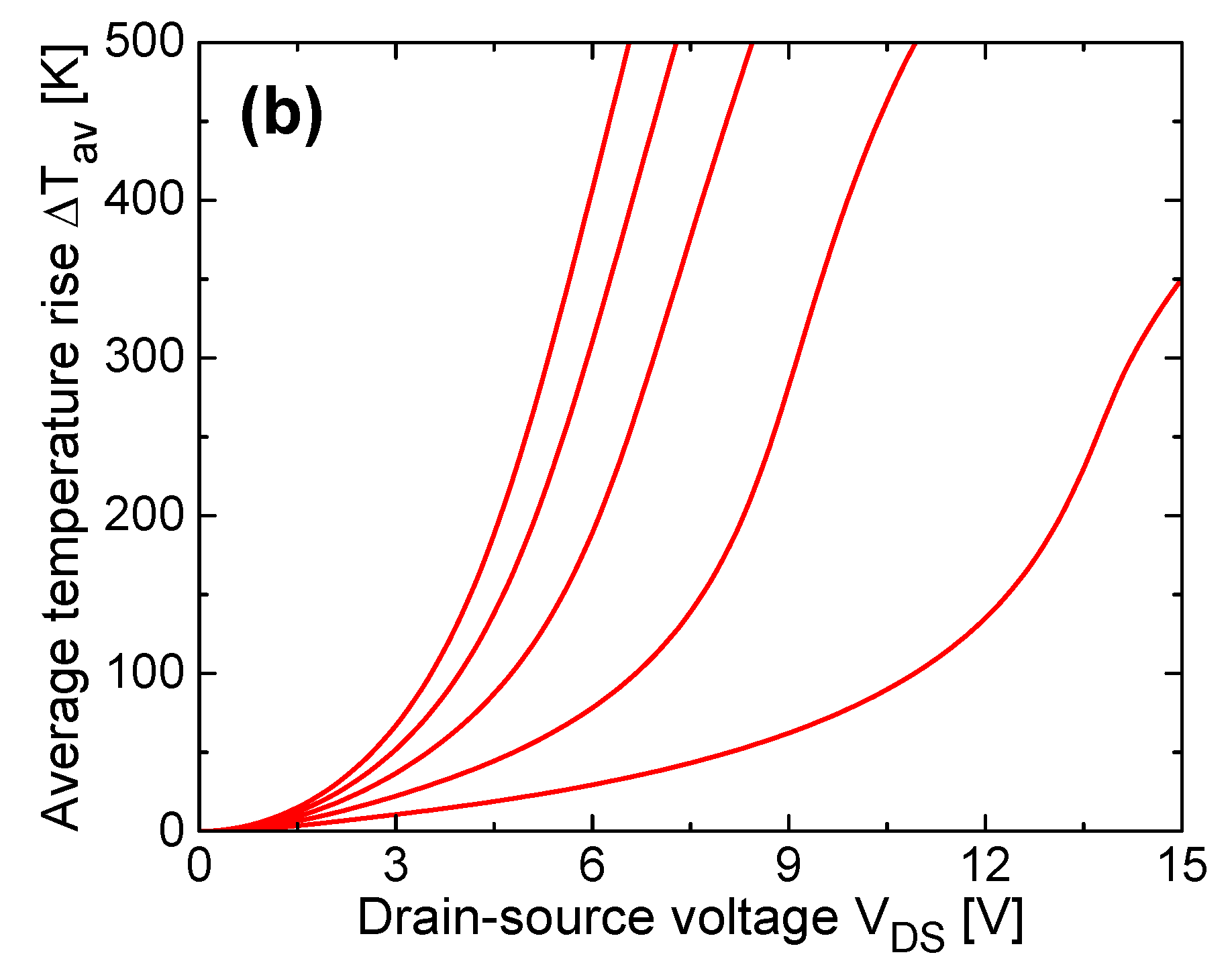
First, the IDVDS output characteristics were determined with a VDS step amounting to 0.1 V under isothermal (at T0) and ET conditions. Isothermal conditions were obtained by deactivating the thermal feedback block. The CPU time needed to simulate a single ET characteristic was nearly 100 s. Results are reported in Figure 17, which also shows the temperature rise above T0 averaged over the effective active area (ΔTav). It can be inferred that the simulation runs were stopped as ΔTav reached 500 K.
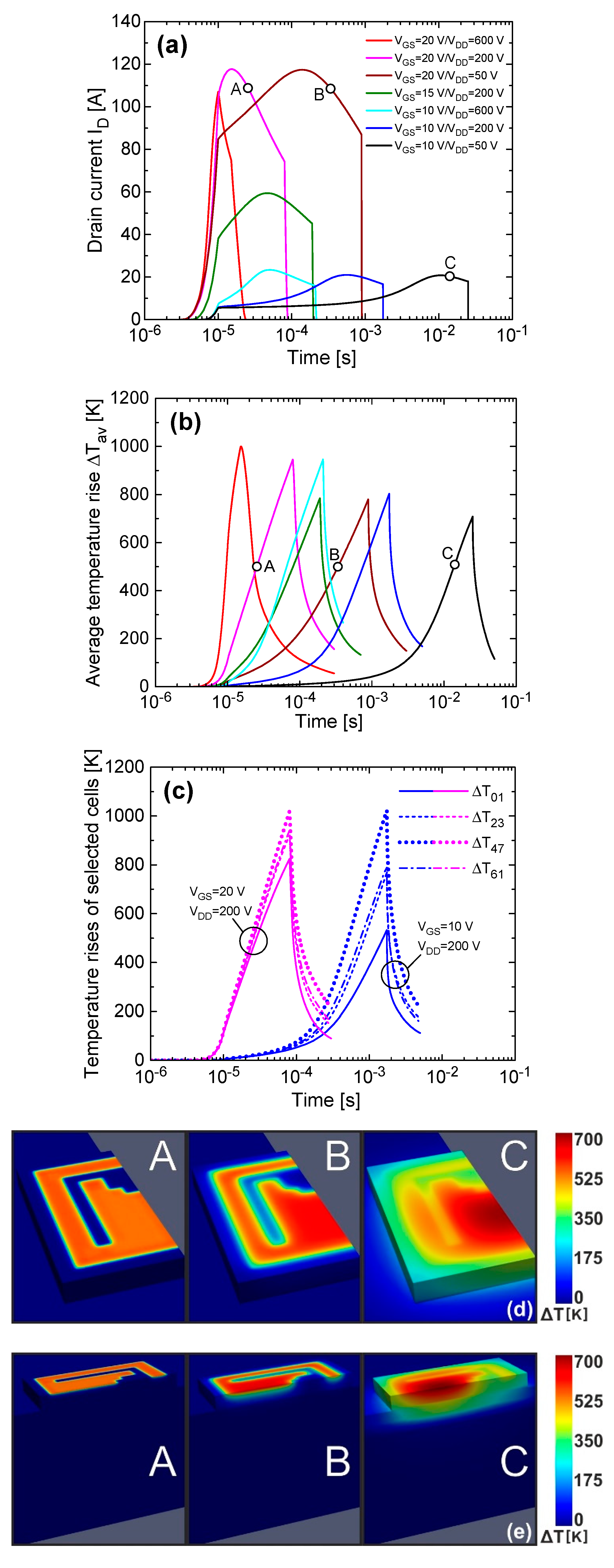
Afterward, SC tests were simulated. Such tests involve large power dissipation, and are typically used to quantify the device robustness under harsh and abnormal events (see e.g., [7,23,25,44,45,46,47], all focused on SiC MOSFETs). In the SC experiment, the DUT is first biased in the OFF state with a given supply voltage applied to the drain, and then turned on with a single gate pulse (a gate resistance RGATE of 50 Ω was considered). The knowledge of the whole temperature distribution over the active area is important, since the value and position of the temperature peak are needed for reliability considerations. The effects of many combinations of gate and supply voltages were examined. Simulation runs were very fast: a single test required about 300 s with a fine time discretization. The total drain current ID conducted by the DUT vs. time is shown in Figure 18a for all the analyzed cases, while Figure 18b illustrates the corresponding temperature rises ΔTav. The first figure reveals that ID first grows due to the strong positive temperature coefficient induced by (i) the reduction in threshold voltage and (ii) the mobility increase (for the lowered Coulomb scattering), and then drops since the negative temperature coefficient triggered by the acoustic-phonon scattering dominates (thermally stable behavior) as all the traps have released electrons [7,25].
The temperature rises ΔT over cells #01, #23, #47, #61 (identified in the layout of Figure 10) are reported in Figure 18c for two cases, namely, VGS = 10 V/VDD = 200 V and VGS = 20 V/VDD = 200 V. From the inspection of the waveforms, it is found that a pronounced temperature nonuniformity takes place in the first case (the inner cell #47 suffers from a ΔT two times higher than that of the top-corner cell #01), which can be explained as follows. The milder bias conditions (VGS = 10 V) allowed the device to safely undergo the test for a longer period, within which the heat had enough time to significantly spread, thereby favoring a stronger impact of the mutual thermal interactions and the consequent exacerbation of temperature gradients.
The whole temperature field in the domain was determined at chosen time instants from the DCTM generated with FANTASTIC in a post-processing step. More specifically, points A (t = 25.5 µs, VGS = 20 V/VDD = 200 V), B (t = 338 µs, VGS = 20 V/VDD = 50 V), and C (t = 14 ms, VGS = 10 V/VDD = 50 V) identified in Figure 18a,b were selected, which approximately share the same ΔTav value, i.e., 500 K. The computed temperature rise maps are shown in Figure 18d (top view) and Figure 18e (side view). As can be seen, despite the same ΔTav,
  • point A, which falls at a time instant close to the beginning of the test, is endowed with a uniform and superficial temperature field, since the heat is still confined in the top active region close to the generation area;
  • the temperature distributions in B and C are increasingly uneven, which is again ascribable to the much longer stress times. In particular, C suffers from a severe temperature focusing over the innermost DUT area, and—as witnessed by the side view—the downward heat had enough time to reach and hit the DBC.
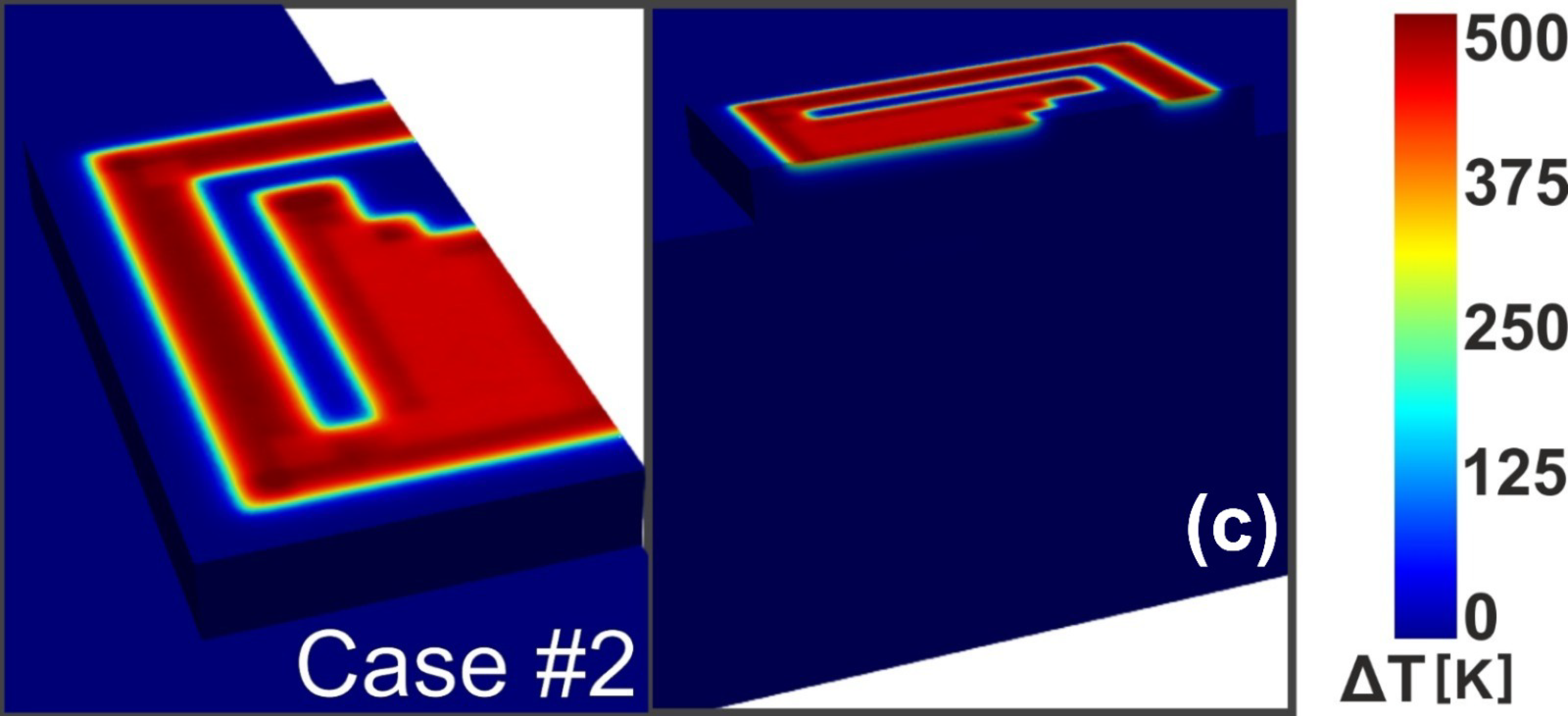
Lastly, the macrocircuit was used to simulate two UIS tests, which are commonly adopted to evaluate the maximum amount of avalanche energy sustainable by the device [8,44]. In the UIS experiment, a load inductor L tied to the drain is first ramped up to a desired current by keeping the DUT in linear mode for a time tON; then the DUT is turned off and brought into avalanche by the inductor, which preserves the current continuity. The tests will be hereinafter denoted as case #1 and #2, the specifics of which are as follows:
  • case #1: VDD = 300 V, L = 4.6 mH, RGATE = 15 Ω
  • case #2: VDD = 600 V, L = 12 mH, RGATE = 15 Ω
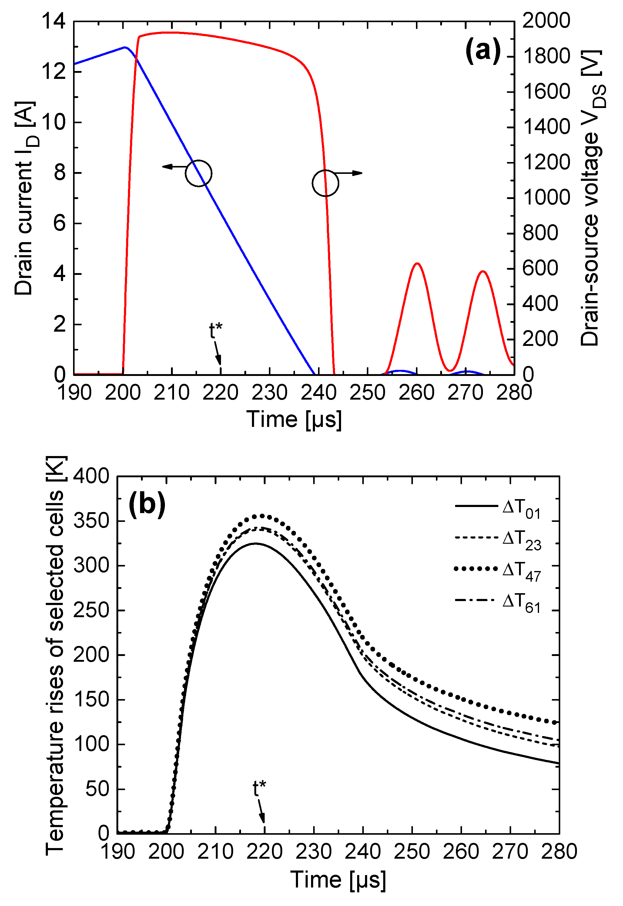
In both cases, a gate voltage equal to 20 V was applied for tON = 200 µs, and then lowered to 0. Again, the time elapsed by PSPICE for a single test was about 300–400 s. Concerning case #1, Figure 19a shows the drain current ID and the drain-source voltage VDS vs. time in the span 190 to 280 µs, while Figure 19b illustrates the temperature rises of cells #01, #23, #47, #61. An almost uniform temperature distribution was found, as witnessed by the map taken at time instant t* = 220 µs, where the dynamic temperature averaged over the active area peaks (Figure 19c).
In case #2, despite the lower drain current IDVDD·tON/L before turn-off (10 A instead of 13 A obtained for case #1), the average temperature reaches higher values due the longer discharging transient, in turn dictated by the higher L, since
d I D d t = B V D S ( T ) V D D L
Results are shown in Figure 20. As can be inferred from Figure 20b, which reports the temperature rises of the selected cells, and from Figure 20c, which depicts the post-processing temperature maps at t* = 240 µs, a slightly more nonuniform temperature field occurs with respect to case #1.

6. Conclusions

In this paper, an advanced circuit-based approach for the static and dynamic electrothermal simulation of multicellular SiC power MOSFETs has been proposed, which—differently from the strategies encountered in the literature—seems to represent a good trade-off between accuracy and efficiency. The device is discretized into a chosen number of elementary cells (heat sources) and turned into a purely-electrical macrocircuit, where (i) the cells are described with subcircuits accounting for the key and harmful influence of SiC/SiO2 interface traps, and (ii) the power-temperature feedback is modeled with an equivalent thermal network. This network is obtained through a fully automated process: first, a 3D mesh representing the device is generated in COMSOL with the support of an in-house routine that elaborates the layout files and makes use of further information about thickness of layers, position/shape of the heat sources, material parameters, and boundary conditions; then, such a mesh is provided as an input to the FANTASTIC tool, which derives a dynamic compact thermal model of the device and the related equivalent network. The macrocircuit can be solved in the environment of any SPICE-like simulator with short CPU time and unlikely occurrence of convergence issues. The effectiveness and efficiency of the proposed strategy have been verified on a 1200 V, 50 A multicellular 4H-SiC VDMOS soldered on a DBC package. It has been shown that the simulation of short-circuit and unclamped inductive switching tests requires only 300–400 s on a normal PC, despite the critical conditions and the fine time discretization, and that potentially-dangerous temperature gradients/hogging can be easily identified. It can be concluded that the proposed approach can be helpful for industry engineers who are in charge of optimizing the thermal design of multicellular power devices in any technology.

Author Contributions

Methodology, V.d.; Software, V.d., L.C., A.P.C., C.S.; Validation, V.d.; Writing–Original Draft Preparation, V.d.; Writing–Review & Editing, V.d.; Supervision, V.d. All authors have read and agreed to the published version of the manuscript.

Funding

This research received no external funding.

Acknowledgments

The funding for the Ph.D. activity of Ciro Scognamillo was generously donated by the Rinaldi family in the memory of Niccolò Rinaldi, a bright Professor and Researcher of University of Naples Federico II, prematurely passed away in 2018.

Conflicts of Interest

The authors declare no conflict of interest.

Nomenclature

AlNaluminum nitride
Al2O3alumina
Cucopper
GaAsgallium arsenide
Sisilicon
SiCsilicon carbide
SiO2silicon dioxide (or oxide)
Si3N4silicon nitride
SnPttin-platinum alloy
DBCdirect-bonded copper
DCTMdynamic compact thermal model
DoFdegree of freedom
DUTdevice under test
ETelectrothermal
FANTASTICFAst Novel Thermal Analysis Simulation Tool for Integrated Circuits
FEMfinite-element method
HBTheterojunction bipolar transistor
IIimpact ionization
ILSinductive load switching
MMmoment matching
MORmodel-order reduction
MOSFETmetal oxide semiconductor field effect transistor
SCshort circuit
TEOLthermal equivalent of the Ohm’s law
TRBtruncated balance
UISunclamped inductive switching
VDMOSvertical double-diffused MOS

References

  1. Östling, M.; Ghandi, R.; Zetterling, C.-M. SiC power devices—Present status, applications and future perspectives. In Proceedings of the IEEE International Symposium on Power Semiconductor Devices and IC’s (ISPSD), San Diego, CA, USA, 23–26 May 2011; pp. 10–15. [Google Scholar]
  2. De Falco, G.; Riccio, M.; Romano, G.; Maresca, L.; Irace, A.; Breglio, G. ELDO-COMSOL based 3D electro-thermal simulations of power semiconductor devices. In Proceedings of the IEEE Annual SEMIconductor THERMal measurement, modeling, and management symposium (SEMI-THERM), San Jose, CA, USA, 9–13 March 2014; pp. 35–40. [Google Scholar]
  3. Chvála, A.; Donoval, D.; Marek, J.; Príbytný, P.; Molnár, M.; Mikolášek, M. Fast 3-D electrothermal device/circuit simulation of power superjunction MOSFET based on SDevice and HSPICE interaction. IEEE Trans. Electron Devices 2014, 61, 1116–1122. [Google Scholar] [CrossRef]
  4. Košel, V.; de Filippis, S.; Chen, L.; Decker, S.; Irace, A. FEM simulation approach to investigate electro-thermal behavior of power transistors in 3-D. Microelectron. Reliab. 2013, 53, 356–362. [Google Scholar] [CrossRef]
  5. Pfost, M.; Boianceanu, C.; Lohmeyer, H.; Stecher, M. Electrothermal simulation of self-heating in DMOS transistors up to thermal runaway. IEEE Trans. Electron Devices 2013, 60, 699–707. [Google Scholar] [CrossRef]
  6. Codecasa, L.; d’Alessandro, V.; Magnani, A.; Rinaldi, N.; Zampardi, P.J. FAst Novel Thermal Analysis Simulation Tool for Integrated Circuits (FANTASTIC). In Proceedings of the IEEE international workshop on THERMal INvestigations of ICs and systems (THERMINIC), Greenwich, London, UK, 24–26 September 2014. [Google Scholar]
  7. d’Alessandro, V.; Magnani, A.; Riccio, M.; Breglio, G.; Irace, A.; Rinaldi, N.; Castellazzi, A. SPICE modeling and dynamic electrothermal simulation of SiC power MOSFETs. In Proceedings of the IEEE International Symposium of Power Semiconductor Devices and IC’s (ISPSD), Waikoloa, HI, USA, 15–19 June 2014. [Google Scholar]
  8. Fayyaz, A.; Romano, G.; Urresti, J.; Riccio, M.; Castellazzi, A.; Irace, A.; Wright, N. A comprehensive study of the avalanche breakdown robustness of silicon carbide power MOSFETs. Energies 2017, 10, 452. [Google Scholar] [CrossRef] [Green Version]
  9. Riccio, M.; d’Alessandro, V.; Romano, G.; Maresca, L.; Breglio, G.; Irace, A. A temperature-dependent SPICE model of SiC power MOSFETs for within and out-of-SOA simulations. IEEE Trans. Power Electron. 2018, 33, 8020–8029. [Google Scholar] [CrossRef]
  10. Mantooth, H.A.; Peng, K.; Santi, E.; Hudgins, J.L. Modeling of wide bandgap semiconductor devices–Part I. IEEE Trans. Electron Devices 2015, 62, 423–433. [Google Scholar] [CrossRef]
  11. Codecasa, L.; d’Alessandro, V.; Magnani, A.; Irace, A. Circuit-based electrothermal simulation of power devices by an ultrafast nonlinear MOS approach. IEEE Trans. Power Electron. 2016, 31, 5906–5916. [Google Scholar] [CrossRef]
  12. Rinaldi, N.; d’Alessandro, V. Theory of electrothermal behavior of bipolar transistors: Part III–Impact ionization. IEEE Trans. Electron Devices 2006, 53, 1683–1697. [Google Scholar] [CrossRef]
  13. Ren, Y.; Xu, M.; Zhou, J.; Lee, F.C. Analytical loss model of power MOSFET. IEEE Trans. Power Electron. 2006, 21, 310–319. [Google Scholar]
  14. Baliga, B.J. Modern Power Devices; Wiley: New York, NY, USA, 1987. [Google Scholar]
  15. Arora, N. MOSFET Modeling for VLSI Simulation: Theory and Practice; World Scientific Publishing Co. Pte. Ltd.: Singapore, 2007. [Google Scholar]
  16. Ólafsson, H.Ö.; Gudjónsson, G.; Allerstam, F.; Sveinbjörnsson, E.Ö.; Rödle, T.; Jos, R. Stable operation of high mobility 4H-SiC MOSFETs at elevated temperatures. Electron. Lett. 2005, 41, 825–826. [Google Scholar]
  17. Wang, J.; Zhao, T.; Li, J.; Huang, A.Q.; Callanan, R.; Husna, F.; Agarwal, A. Characterization, modeling, and application of 10-kV SiC MOSFETs. IEEE Trans. Electron Devices 2008, 55, 1798–1806. [Google Scholar] [CrossRef]
  18. Chen, S.; Cai, C.; Wang, T.; Guo, Q.; Sheng, K. Cryogenic and high temperature performance of 4H-SiC power MOSFETs. In Proceedings of the Annual IEEE Applied Power Electronics Conference and Exposition (APEC), Long Beach, CA, USA, 17–21 March 2013; pp. 207–210. [Google Scholar]
  19. Spirito, P.; Breglio, G.; d’Alessandro, V.; Rinaldi, N. Thermal instabilities in high current power MOS devices: Experimental evidence, electro-thermal simulations and analytical modeling. In Proceedings of the IEEE International Conference on MIcroELectronics (MIEL), Niš, Yugoslavia, 12–15 May 2002; pp. 23–30. [Google Scholar]
  20. Spirito, P.; Breglio, G.; d’Alessandro, V.; Rinaldi, N. Analytical model for thermal instability of low voltage power MOS and S.O.A. in pulse operation. In Proceedings of the IEEE International Symposium on Power Semiconductor Devices and IC’s (ISPSD), Santa Fe, NM, USA, 3–7 June 2002; pp. 269–272. [Google Scholar]
  21. Pérez-Tomás, A.; Brosselard, P.; Godignon, P.; Millán, J.; Mestres, N.; Jennings, M.R.; Covington, J.A.; Mawby, P.A. Field-effect mobility temperature modeling of 4H-SiC metal-oxide-semiconductor transistors. J. Appl. Phys. 2006, 100, 114508. [Google Scholar] [CrossRef]
  22. Cheng, L.; Agarwal, A.K.; Dhar, S.; Ryu, S.-H.; Palmour, J.W. Static performance of 20 A, 1200 V 4H-SiC power MOSFETs at temperatures of −187 °C to 200 °C. J. Electron. Mater. 2012, 41, 910–914. [Google Scholar] [CrossRef]
  23. Huang, X.; Wang, G.; Li, Y.; Huang, A.Q.; Baliga, B.J. Short-circuit capability of 1200V SiC MOSFET and JFET for fault protection. In Proceedings of the Annual IEEE Applied Power Electronics Conference and Exposition (APEC), Long Beach, CA, USA, 17–21 March 2013; pp. 197–200. [Google Scholar]
  24. TCAD Sentaurus User’s Manual, Synopsis, 2015. Available online: https://www.synopsys.com/silicon/tcad/device-simulation/sentaurus-device.html (accessed on 25 May 2020).
  25. Castellazzi, A.; Funaki, T.; Kimoto, T.; Hikihara, T. Thermal instability effects in SiC power MOSFETs. Microelectron. Reliab. 2012, 52, 2414–2419. [Google Scholar] [CrossRef]
  26. d’Alessandro, V.; Magnani, A.; Riccio, M.; Iwahashi, Y.; Breglio, G.; Rinaldi, N.; Irace, A. Analysis of the UIS behavior of power devices by means of SPICE-based electrothermal simulations. Microelectron. Reliab. 2013, 53, 1713–1718. [Google Scholar] [CrossRef]
  27. Bazzano, G.; Cavallaro, D.G.; Greco, G.; Grimaldi, A.; Rinaudo, S. Stress and reliability of power devices: An innovative thermal analysis approach to predict a device’s lifetime. In Proceedings of the International Exhibition & Conference for Power Electronics, Intelligent Motion, Power Quality (PCIM Europe), Nuremberg, Germany, 17–19 May 2011; pp. 117–123. [Google Scholar]
  28. Joyce, W.B. Thermal resistance of heat sinks with temperature-dependent conductivity. Solid State Electron. 1975, 18, 321–322. [Google Scholar] [CrossRef]
  29. Poulton, K.; Knudsen, K.L.; Corcoran, J.J.; Wang, K.-C.; Pierson, R.L.; Nubling, R.B.; Chang, M.-C.F. Thermal design and simulation of bipolar integrated circuits. IEEE J. Solid State Circuits 1992, 27, 1379–1387. [Google Scholar] [CrossRef]
  30. PSPICE User’s Manual, Cadence OrCAD 16.5, 2011. Available online: https://www.orcad.com/ (accessed on 25 May 2020).
  31. Li, H.; Munk-Nielsen, S.; Bęczkowski, S.; Wang, X. A novel DBC layout for current imbalance mitigation in SiC MOSFET multichip power modules. IEEE Trans. Power Electron. 2016, 31, 8042–8045. [Google Scholar] [CrossRef]
  32. Suganuma, K.; Kim, S. Ultra heat-shock resistant die attachment for silicon carbide with pure zinc. IEEE Electron Device Lett. 2010, 31, 1467–1469. [Google Scholar] [CrossRef]
  33. Catalano, A.P.; Scognamillo, C.; Castellazzi, A.; d’Alessandro, V. Optimum thermal design of high-voltage double-sided cooled multi-chip SiC power modules. In Proceedings of the IEEE International Workshop on THERMal INvestigations of ICs and Systems (THERMINIC), Lecco, Italy, 25–27 September 2019. [Google Scholar]
  34. COMSOL Multiphysics User’s Guide, Release 5.2A, 2016. Available online: https://www.comsol.it/ (accessed on 25 May 2020).
  35. d’Alessandro, V.; Catalano, A.P.; Codecasa, L.; Zampardi, P.J.; Moser, B. Accurate and efficient analysis of the upward heat flow in InGaP/GaAs HBTs through an automated FEM-based tool and Design of Experiments. Int. J. Numer. Model. Electron. Netw. Devices Fields 2019, 32. [Google Scholar]
  36. Harris, G.L. Properties of Silicon Carbide; INSPEC, the Institution of Electrical Engineers: London, UK, 1995. [Google Scholar]
  37. Goldberg, Y.; Levinshtein, M.E.; Rumyantsev, S.L. Silicon Carbide. In Properties of Advanced Semiconductor Materials: GaN, AlN, InN, BN, SiC, SiGe; Levinshtein, M.E., Rumyantsev, S.L., Shur, M.S., Eds.; John Wiley & Sons, Inc.: New York, NY, USA, 2001; Volume 5, pp. 93–148. [Google Scholar]
  38. Gomes de Mesquita, A.H. Refinement of the crystal structure of SiC type 6H. Acta Crystallogr. 1967, 23, 610–617. [Google Scholar] [CrossRef]
  39. Palankovski, W.; Quay, R. Analysis and Simulation of Heterostructure Devices; Springer: New York, NY, USA, 2004. [Google Scholar]
  40. Joshi, R.P.; Neudeck, P.G.; Fazi, C. Analysis of the temperature dependent thermal conductivity of silicon carbide for high temperature applications. J. Appl. Phys. 2000, 88, 265–269. [Google Scholar] [CrossRef]
  41. Lienhard, I.V.; Lienhard, H. A Heat Transfer Textbook; Phlogiston Press: Cambridge, MA, USA, 2008. [Google Scholar]
  42. Codecasa, L.; D’Amore, D.; Maffezzoni, P. Compact modeling of electrical devices for electrothermal analysis. IEEE Trans. Circuits Syst. I Fundam. Theory Appl. 2003, 50, 465–476. [Google Scholar] [CrossRef]
  43. Codecasa, L.; Catalano, A.P.; d’Alessandro, V. A Priori error bound for moment matching approximants of thermal models. IEEE Trans. Compon. Packag. Manuf. Technol. 2019, 9, 2383–2392. [Google Scholar] [CrossRef]
  44. Fayyaz, A.; Yang, L.; Castellazzi, A. Transient robustness testing of silicon carbide (SiC) power MOSFETs. In Proceedings of the European Conference on Power Electronics and Applications (EPE), Lille, France, 2–6 September 2013. [Google Scholar]
  45. Nguyen, T.-T.; Ahmed, A.; Thang, T.V.; Park, J.-H. Gate oxide reliability issues of SiC MOSFETs under short-circuit operation. IEEE Trans. Power Electron. 2015, 30, 2445–2455. [Google Scholar] [CrossRef]
  46. Romano, G.; Maresca, L.; Riccio, M.; d’Alessandro, V.; Breglio, G.; Irace, A.; Fayyaz, A.; Castellazzi, A. Short-circuit failure mechanism of SiC power MOSFETs. In Proceedings of the IEEE International Symposium on Power Semiconductor Devices and IC’s (ISPSD), Hong Kong, China, 10–14 May 2015; pp. 345–348. [Google Scholar]
  47. Cavallaro, D.; Pulvirenti, M.; Zanetti, E.; Saggio, M. Capability of SiC MOSFETs under short-circuit tests and development of a thermal model by finite element analysis. Mater. Sci. Forum 2019, 963, 788–791. [Google Scholar] [CrossRef]
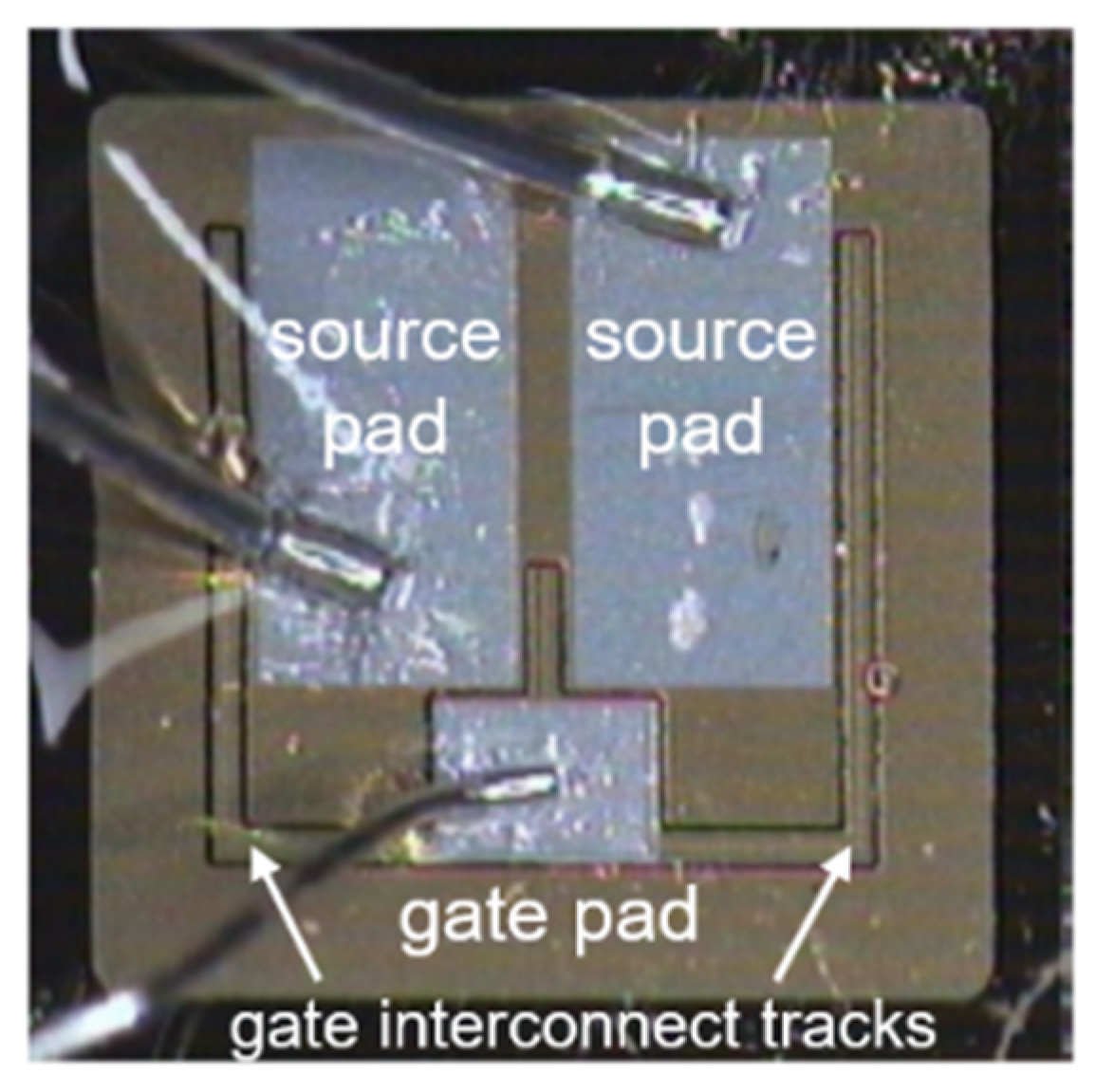
Figure 1. Device under test (bare die).
Energies 13 04563 g001
Figure 2. Sketch of the transistor representation.
Energies 13 04563 g002
Figure 3. Threshold voltage VTH vs. baseplate temperature TB: comparison between experimental data (red circles) and model (14) (solid blue line) with optimized parameters.
Energies 13 04563 g003
Figure 4. Current factor K against baseplate temperature TB: comparison between experimental data (red circles) and model (15) and (16) (solid blue line) with optimized parameters.
Energies 13 04563 g004
Figure 5. IDVGS transfer characteristics of the DUT at VDS = 20 V and TB = 303, 348, 423, and 473 K: comparison between experimental data (red circles) and model (2) with calibrated parameters for the VTH and K formulations (solid blue lines).
Energies 13 04563 g005
Figure 6. IDVDS output characteristics of the DUT at VGS = 10, 12.5, 15, 17.5, 20 V and TB = 303 K: comparison between experimental data (red circles) and the model described in Section 2, where Rdrift is given by (10), (11) with tuned parameters (solid blue lines).
Energies 13 04563 g006
Figure 7. Modeled IDVGS transfer characteristics at VDS = 20 V and TB = 303, 348, 423, and 473 K: comparison between the real DUT (blue lines) and the traps-free counterpart (magenta). ZTC stands for zero-temperature coefficient.
Energies 13 04563 g007
Figure 8. Temperature coefficient αT of the drain current at TB = T0 and VDS = 20 V for the real DUT (blue line) and its traps-free version (magenta).
Energies 13 04563 g008
Figure 9. Sketch of the SPICE-compatible subcircuit for the transistor cell.
Energies 13 04563 g009
Figure 10. Discretization of the effective active area of half DUT. Left: PSPICE subcircuit with hierarchical blocks corresponding to the transistor cells; center: cell numbering, with evidenced cells of interest for the ET analysis presented in Section 5; right: connections between some adjacent cells.
Energies 13 04563 g010
Figure 11. Sketch of the top view (not to scale) of the domain to be electrothermally simulated. All dimensions are expressed in mm.
Energies 13 04563 g011
Figure 12. Sketch of the cross-section (not to scale) of the domain to be electrothermally simulated. All dimensions are expressed in µm.
Energies 13 04563 g012
Figure 13. 3D representation of the geometry of the domain under test in the COMSOL Multiphysics environment (draw mode): (a) whole structure and (b) magnification of the 4H-SiC VDMOS die.
Energies 13 04563 g013
Figure 14. 3D tetrahedral mesh of the domain under test in the COMSOL Multiphysics environment (mesh mode): (a) whole structure and (b) magnification of the 4H-SiC VDMOS die.
Energies 13 04563 g014
Figure 15. DCTM equivalent thermal network (after Codecasa et al. [6]).
Energies 13 04563 g015
Figure 16. Schematic representation of the proposed strategy to perform a fully coupled ET analysis in a circuit simulation tool: the feedback loop between the electrical circuit (left) and the thermal feedback block (TFB, right) relying on the DCTM-based equivalent network is highlighted.
Energies 13 04563 g016
Figure 17. (a) IDVDS output characteristics determined with the proposed approach under isothermal (dashed blue lines) and ET (solid red) conditions; (b) temperature rise ΔTav = TavT0 corresponding to the ET conditions, Tav being the temperature averaged over the effective active area.
Energies 13 04563 g017aEnergies 13 04563 g017b
Figure 18. Simulated SC test: (a) drain current ID vs. time for seven VGS/VDD combinations; (b) corresponding temperature rises averaged over the effective active area; (c) temperature rises of the individual cells highlighted in Figure 10 for 2 cases; (d) top and (e) side views of the 3D temperature rise maps determined at points A, B, and C shown in (a) and (b).
Energies 13 04563 g018
Figure 19. Simulated UIS test, case #1: (a) drain current ID and drain-source voltage VDS against time; (b) temperature rises of the individual cells identified in Figure 10; (c) top and side views of the temperature rise maps calculated at time instant t* = 220 µs shown in (a) and (b).
Energies 13 04563 g019aEnergies 13 04563 g019b
Figure 20. Simulated UIS test, case #2: (a) drain current ID and drain-source voltage VDS vs. time; (b) temperature rises of the individual cells highlighted in Figure 10; (c) top and side views of the temperature rise maps calculated at time instant t* = 240 µs identified in (a) and (b).
Energies 13 04563 g020aEnergies 13 04563 g020b
Table 1. Optimized parameter values used in the transistor model.
ParameterDefinitionValue
VTH(T0)threshold voltage at reference temperature T06.398 V
VTH∞parameter of the threshold voltage model2.05 V
aVTHtemperature coefficient of the threshold voltage6 mK−1
K(T0)current factor at reference temperature T00.422 A/V2
amparameter of the exponent m accounting for the mobility temperature dependence0.24
bmparameter of the exponent m accounting for the mobility temperature dependence2
cmparameter of the exponent m accounting for the mobility temperature dependence1.02
dmparameter of the exponent m accounting for the mobility temperature dependence0.09
RJFET(T0)resistance of the accumulation and JFET regions at reference temperature T0, Vdrift » V1, and VGS = V20.235 Ω
mRJFETexponent for the temperature dependence of the resistance RJFET−1.3
V1parameter to account for the RJFET dependence on Vdrift13 V
V2parameter to account for the RJFET dependence on VGS20 V
ηexponent to account for the RJFET dependence on VGS3.45
Repi(T0)resistance of the deep epilayer region at reference temperature T010 mΩ
mRepiexponent to account for the potential temperature dependence of the resistance Repi0
BVDS(T0)drain-source breakdown voltage at reference temperature T01750 V
mIIparameter of the avalanche multiplication factor M1.8
nIIparameter of the avalanche multiplication factor M2.9
αIItemperature coefficient of the breakdown voltage BV0.18 mK-1
βIIcoefficient to account for the ID dependence of factor M0 A−1
RIIresistance to account for the ID dependence of factor M10 Ω
CGD0zero-bias gate-drain capacitance0.85 nF
CGDMINminimum gate-drain reverse-biased capacitance0.01 nF
V *gate-drain capacitance parameter2 V
CDS0zero-bias drain-source capacitance2.8 nF
CDSMINminimum drain-source reverse-biased capacitance0.06 nF
V **drain-source capacitance parameter10 V
Table 2. Properties of the materials composing the assembly.
Materialk(T0)
(W/mK)
cp
(J/KgK)
ρ
(Kg/m3)
αβ
(W/mK2)
4H-SiC370 [36,37]690 [37]3211 [38,39]
(value common to 4H-SiC and 6H-SiC)
1.29 [40]
Al240 [41]905 [41]2707 [41] 0.04 [41]
SnPt68.8 [41]228 [41]7310 [41] 0.02 [41]
Ni89.5 [41]445 [41]8906 [41] 0.08 [41]
Ag427 [41]236 [41]10,524 [41] 0.07 [41]
poly-Si40 [39]920 [39]2330 [39]
SiO21.38 [39]709 [39]2203 [39]−0.33 [39]
Al2O328 [39]796 [39]3900 [39]1 [39]
Cu396.8 [41]384 [41]8954 [41] 0.05 [41]
Si3N418.5 [39]787 [39]3100 [39]−0.33 [39]