Article

Wide Input Voltage Range Operation of the Series Resonant DC-DC Converter with Bridgeless Boost Rectifier

1
Department of Electrical Power Engineering and Mechatronics, Tallinn University of Technology, 19086 Tallinn, Estonia
2
Smart City Center of Excellence (Finest Twins), Tallinn University of Technology, 19086 Tallinn, Estonia
*
Author to whom correspondence should be addressed.
Energies 2020, 13(16), 4220; https://doi.org/10.3390/en13164220
Submission received: 21 July 2020 / Revised: 12 August 2020 / Accepted: 13 August 2020 / Published: 14 August 2020
(This article belongs to the Section A1: Smart Grids and Microgrids)

Abstract

:
The series resonant DC-DC converter (SRC) can regulate the input voltage in a wide range at a fixed switching frequency. In this work, the bridgeless rectifier, which is utilized intensively in the applications of the power factor correction, has been integrated into the SRC as a voltage step-up cell at the output-side of the SRC. It is shown that the conventional overlapping pulse-width modulation (PWM) of the two metal oxide semiconductor field-effect transistors MOSFETs in this rectification cell limits the input voltage regulation range of the converter due to excessive power losses in abnormal operating conditions. The abnormal operating conditions occur when the instantaneous voltage across the resonant capacitor is larger than the secondary voltage of the isolation transformer. This happens at high values of the DC voltage gain, i.e., low input voltages and high currents, which causes the resonant current to flow in the reverse direction in the same half-cycle through a parasitic path formed by overlapping PWM of the rectifier MOSFETs. The abnormal operation results in additional conduction loss in the converter as the MOSFETs of the bridgeless boost rectifier turn on at high current at the beginning of each half of the switching period. Accordingly, the overall efficiency of the converter significantly deteriorates. This paper proposes the hybrid PWM aiming to improve the efficiency of the SRC with a bridgeless boost rectifier in a wide input voltage regulation range. The converter swaps between the overlapping and the proposed short-pulse PWM schemes to drive the MOSFETs in the bridgeless boost rectifier. The transition between the two PWM schemes is defined according to the boundary condition that relies upon the operating point of the converter power and the input voltage. The proposed hybrid PWM scheme is analyzed and compared to the overlapping PWM at different levels of the input voltage and the load power. A 300 W prototype was studied in the laboratory to show the feasibility of the proposed hybrid PWM scheme with the closed-loop control system to switch between the two PWM schemes.

Graphical Abstract

1. Introduction

With the high growth of the cumulative installed power of the photovoltaic (PV) modules around the world, their cost is being reduced significantly [1]. The reduction of their cost resulted in the emergence of new cost-sensitive PV applications in residential and small commercial sectors. New technologies, such as building-integrated or building-attached PV [2,3,4], can achieve the best performance when combined with DC distribution [5]. There, the galvanically isolated DC-DC converters are needed to interface individual PV modules into a DC bus. Such DC-DC converters should be capable of regulating the input voltage in a wide range of the possible PV module voltages [6]. Also, the considered converters should provide high conversion efficiency in a wide range of input power as well as high power density [7]. This could be realized either by the synthesis of new topologies or the development of new PWM schemes to enhance the existing topologies [8].
The series resonant converter (SRC) is considered a promising solution for regulating the input voltage over a wide range. The SRC allows for transferring the power from the input to the load during the majority of the switching period, which improves the isolating transformer utilization. Also, it can achieve soft-switching operation when the switching frequency is selected close to the resonant frequency [7,8]. In the conventional SRC, the soft-switching conditions are fulfilled in the primary side semiconductors that are turned on a zero voltage switching. At the same time, the output-side diodes are turned off at zero current. Furthermore, the leakage inductance of the transformer is utilized as a part of the resonant tank, and thus the cost and size of the converter could be reduced as a result. On the other hand, conventional SRC usually employs the variable frequency control and thus provides only voltage step-down operation and suffers from poor controllability at low power. Therefore, the new approach based on the SRC was recently explored. It utilizes a resonant tank with the quality factor of much less than unity, and pulse-width modulation (PWM) to achieve input voltage buck-boost functionality.
Considering the buck-boost operation, the SRC has to be designed to achieve the best efficiency at the nominal input voltage in the vicinity of the most probable operating point of the converter. At the nominal voltage, the SRC performs neither voltage boost nor buck and thus achieves the highest efficiency where the full soft-switching of the semiconductors is guaranteed. When the input voltage has a higher value than the nominal voltage, the SRC can buck the input voltage by employing the phase shift PWM [7,9,10]. Recently, many boosting cells have been evolved to address SRC operation at the input voltage below the nominal value, i.e., the boost operating mode of the SRC [11,12,13,14,15,16,17]. In the boost mode, the SRC is designed to operate at a fixed switching frequency near its resonant frequency to ensure the highest efficiency. Also, the boosting cell is integrated into the secondary side of the isolating transformer to reduce the switching losses where the current is low in the high voltage side of the transformer. Moreover, the positive and negative half-cycles in these methods are symmetrical except in [12], which has a single boosting interval within the switching period. In [15], the synchronous rectification is used to avoid the conduction of the body diodes of the MOSFETs. Although this modulation method could improve the efficiency of the converter, the complexity and the cost of the system could be increased on the other side.
This study is focused on the SRC operation with the bridgeless boost rectifier proposed in [11]. This case study was selected as it showed high overall performance and symmetrical operation of the transformer, which allow extending theoretical findings to other symmetrical boost rectifier topologies. This paper analyzes the operation of the case study topology in a wide range of the input voltage and power and demonstrates limitations not know before. The input voltage and current range limitations are associated with the operation modes of the resonant capacitor. When the voltage ripple of the resonant capacitors exceeds a certain critical value, the symmetrical overlapping modulation of the rectifier MOSFETs establishes a parasitic current path generating excessive power losses. The abnormal operating conditions could be avoided with a new modulation scheme where the rectifier MOSFETs are turned on only during the boosting time interval to avoid the resonant current flowing in the reverse direction. By exploiting the advantages of each PWM scheme in the best region of operation, the considered converter based on the SRC and the bridgeless boost rectifier can reserve the highest efficiency over all the input voltage range.
The remainder of the paper starts with Section 2 that shows a previously unidentified abnormal operating mode of the case study SRC topology. Section 3 introduces a new PWM scheme to be applied where the abnormal operating mode would otherwise appear and provides an analysis of the boundary condition to switch between the two overlapping and the proposed PWM schemes. The experimental verification results are discussed in Section 4. Finally, Section 5 concludes the paper.

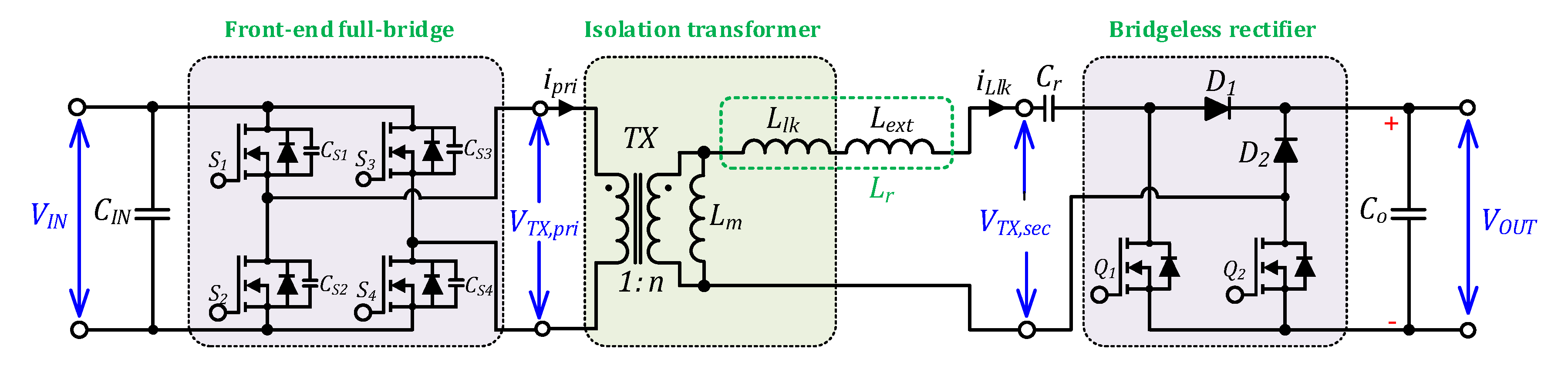
2. Analysis SRC with the Bridgeless Rectifier Controlled with the Overlapping PWM

The bridgeless rectifier cell is commonly used in the applications of the power factor correction [18,19], and it has been implemented in the SRC to regulate the input voltage variations in [11] for the converter shown in Figure 1. The bridgeless rectifier cell has two switches (Q1, Q2) at the bottom of each leg and two diodes at the top (D1, D2). These switches are responsible for the implementation of the boost functionality in the converter. The control signals of the two MOSFETs of the bridgeless rectifier are overlapping during the boosting interval. This results in the short-circuiting of the transformer secondary winding connected in series with the resonant tank. As a result, the resonant inductor can act as an ac boost inductor and thus store energy supplied from the input voltage and the resonant capacitor. These switches (Q1 and Q2 in Figure 1) implement the synchronous rectification in each half-cycle after the boosting interval ends, and the peak-to-peak voltage of the resonant capacitor depends on the converter operating point of the load power and input voltage. At some operating points, especially at the low input voltage, the instantaneous voltage of the resonant capacitor becomes larger than the equivalent voltage of the transformer secondary winding. In the normal operating conditions, the converter enters into the discontinuous conduction mode (free-wheeling state) when the resonant current drops to zero after a boosting time interval. On the other hand, the synchronous rectification resulting from the overlapping PWM scheme of the Q1 and Q2 along with the high voltage ripple of the resonant capacitor result in the resonant current flowing into the reverse direction after reaching zero value. The combination of these factors results in the abnormal operating mode of the SRC, which has not been described in the SRC previously. As a result, the conduction losses in the transformer would increase as the root mean square RMS current is high in the abnormal mode. Also, the semiconductor components of the converter are hard switching at a high current. Hence, the converter efficiency drops significantly at these abnormal operating conditions.
This section aims to describe the operating principle of the case study topology of SRC with the bridgeless rectifier in the abnormal operating conditions, and consequently, analyze the drawbacks of the overlapping PWM scheme. The input voltage VIN feeds the primary winding of the isolating transformer TX through the full-bridge inverter at the front-end side. Besides, the semiconductors in the same leg of the bridge are modulated complementary with a short dead-time in the boosting mode. The isolating transformer steps up the input voltage by the turns ratio n and provides electrical isolation to increase the safety level of the circuit. The resonant tank consists of the resonant capacitor, Cr, and the resonant inductor Lr, which comprises the leakage inductance of the transformer Llk, and an external inductance Lext. This external inductor is usually exploited when the leakage inductance of the transformer is small to enhance the converter efficiency as the larger values of Lr minimizes the RMS current in the circuit components [16]. The resonant frequency Fr is a function in the resonant tank parameters, according to Equation (1):
F r = 1 2 π L r C r
The two decoupled capacitors (CIN and CO) are harnessed to filter the input and output voltages, respectively. In this paper, the term Δ V C r refers to the peak-to-peak ripple of the voltage across the resonant capacitor, which changes with the converter power P, and the input voltage VIN according to Equation (2). The circuit has been well-analyzed in the boosting case with the overlapping PWM scheme in [11], but only for the normal operating condition when Δ V C r 2 n V I N . Therefore in this paper, the circuit will be analyzed only for the abnormal condition when Δ V C r > 2 n V I N , as the operation of the circuit differs significantly from that described in [11], and thus, the existing steady-state mathematical model is not valid. It is worth mentioning that the abnormal operating condition could happen only at a low input voltage and depends on the voltage ripple value of the resonant capacitor, as follows from Equation (2):
Δ V C r = P T S W 2 n V I N C r
The steady-state waveforms of the converter are given in Figure 2 for Δ V C r > 2 n V I N . The dead-time is inserted between the control signal of the primary switches in the same leg to avoid the short-circuit across the input terminals. The magnetizing current Im has a positive slope when the positive voltage is applied to the transformer windings and vice versa. The peak value of Im does not depend on the load power; it is defined by the input voltage, the magnetizing inductance of the transformer Lm, and the switching frequency FSW:
I m = n V I N 2 L m F S W .
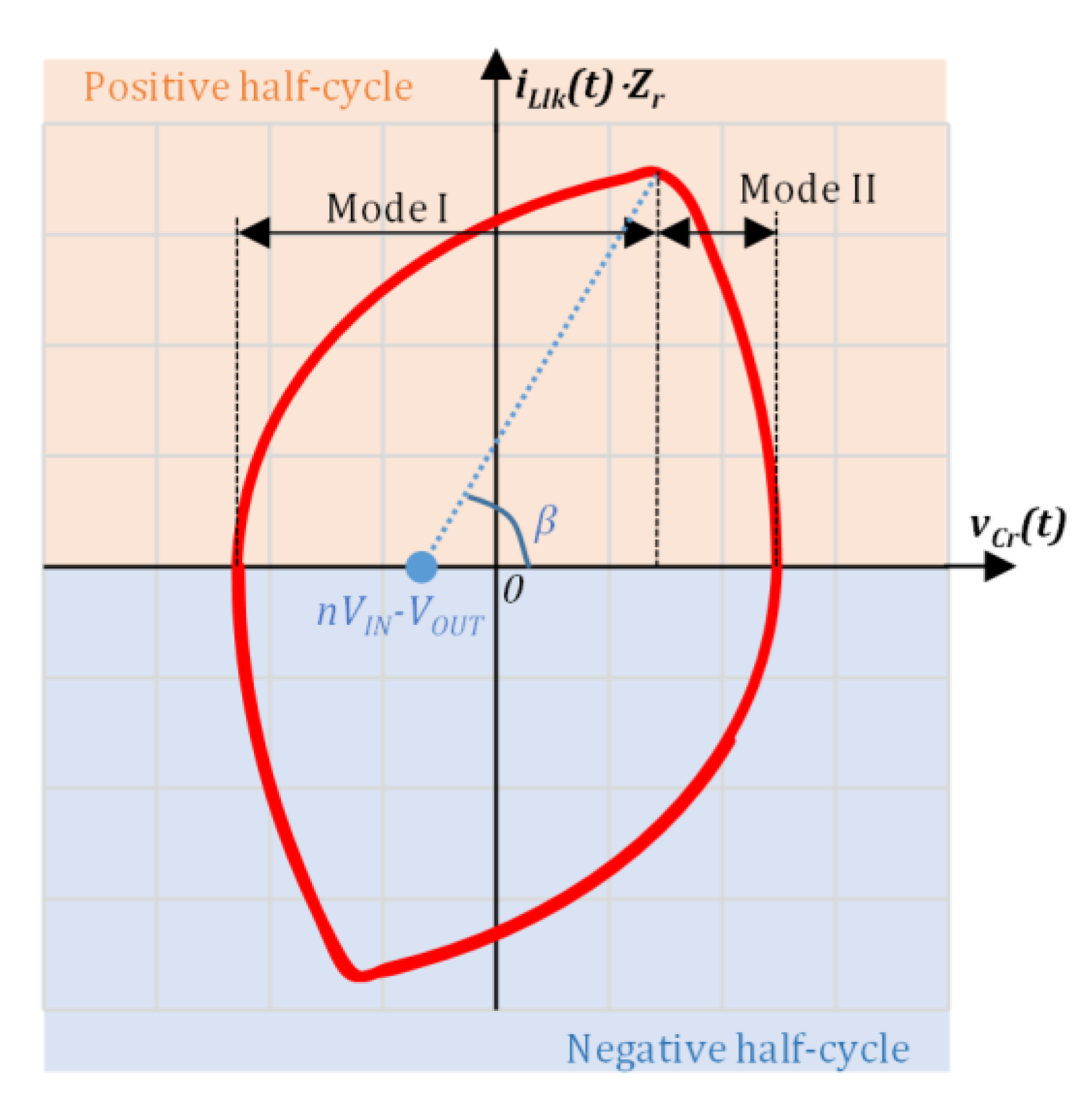
The considered state variables are the resonant current iLlk(t) and the resonant capacitor voltage vCr(t). The state-plane trajectory of the resonant tank is sketched in Figure 3.
The shape of the trajectory varies when the converter operating point changes. However, the positive and negative half-cycles of the converter operation are always symmetrical so that the circuit operation will be analyzed only for the positive half-cycle. In the abnormal condition, the state variables of the resonant tank are continuous and correspond to a piecewise-sinusoidal function in time during the whole switching period. The operation of the converter is analyzed, assuming the system is lossless and the output voltage is ripple-free as the capacitance CO is high. The four operating modes of the converter during the positive half-cycle can be given as below:
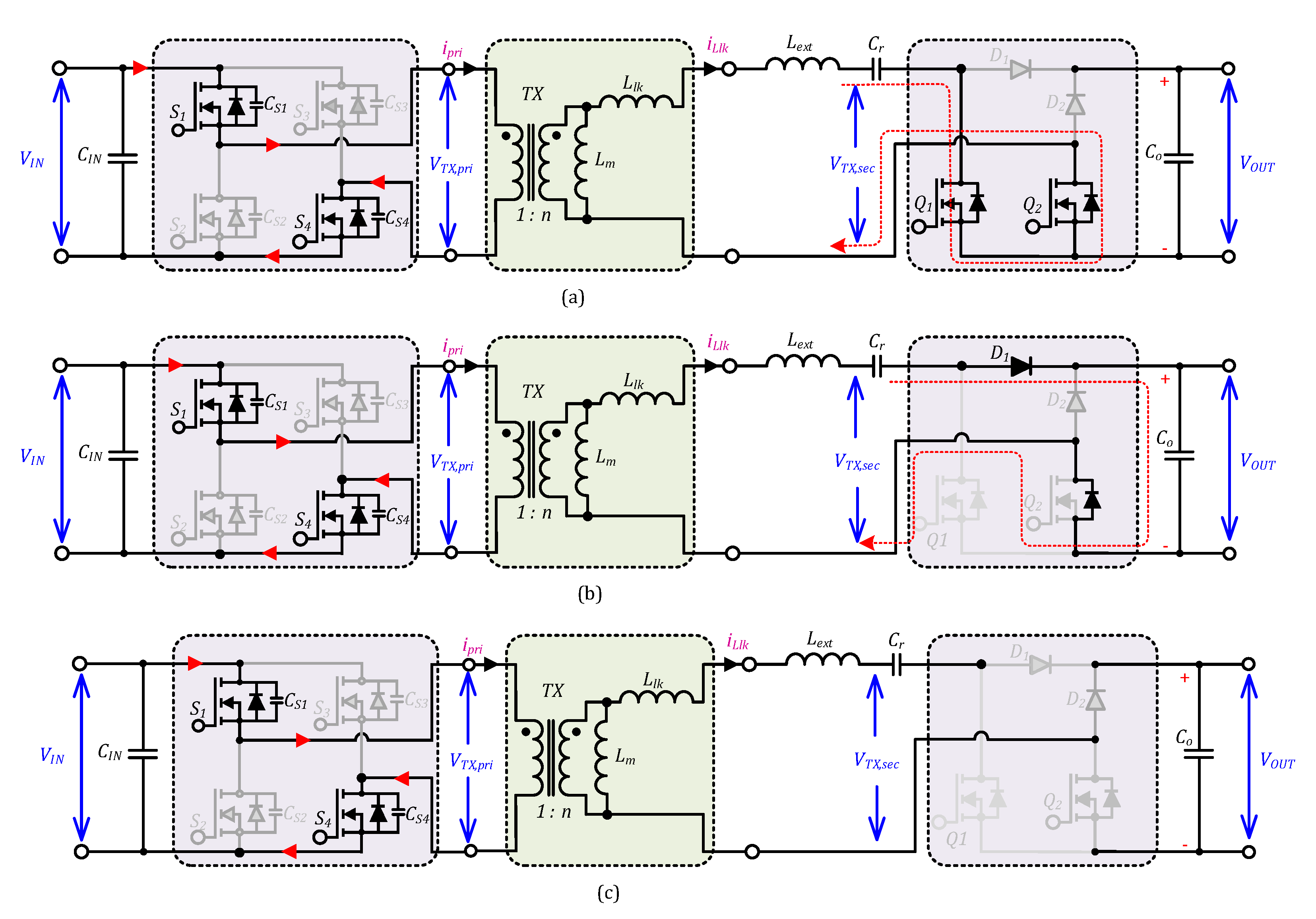
Mode I [t0 < t ≤ t1]: This interval corresponds to a half of the boosting duty cycle of the converter. A corresponding equivalent circuit and a simplified equivalent circuit of the converter during this mode are given in Figure 4a and Figure 5a, respectively. Unlike in the normal operating conditions, the resonant current has an initial value of I0 at the instant t0. The primary winding of the isolating transformer is fed with a positive voltage by turning on the switches S1 and S4. The switch Q2 will turn on at the high current of the resonant inductor while Q1 is still conducting from the previous half-cycle. The voltage across the resonant capacitor has an initial value of V0 at the instant t0, which is larger than the value of Δ V C r 2 . Therefore, the resonant inductor current continues flowing in the same positive direction until the boosting interval ends.
Mode II [t1 < t ≤ t2]: The equivalent and the simplified equivalent circuits are given in Figure 4b and Figure 5b, respectively. The switch Q1 is turned off, and the diode D1 is forward-biased by the resonant inductor current. Consequently, there is a direct connection to the load, and the energy stored in the resonant inductance is releasing to the load. This mode ends when the current drops to the zero value at the instant t2, when the maximum value of the resonant capacitor voltage is achieved.
Mode III [t2 < t ≤ t3]: This is considered the new operating mode of the converter, which was not described in [11]. The equivalent circuit and the simplified equivalent circuit are given in Figure 4c and Figure 5c. The current of the inductor begins to flow in the negative direction through the parasitic current path created by the switch Q1 and the body diode of the switch Q2. The transformer voltage is still positive during this mode. The capacitor voltage has the maximum value that is larger than the equivalent secondary winding voltage. In this mode, there is no direct connection between the input source and the load.
Mode IV [t3 < t ≤ t4]: The dead-time between the switches is applied during this mode. The switches S1 and S4 are turned off. The inductor current is still flowing in the same direction until the next time-interval. Also, the resonant capacitor continues discharging its energy in the inductor. The primary current has a non zero value.

3. Proposed PWM Scheme for the Bridgeless SRC

It was shown in the previous section that the switches of the converter turn on at high current in the case of the abnormal operating conditions. Accordingly, this section is dedicated to the development of a new modulation scheme that avoids the parasitic current path and keeps the converter in the freewheeling state after the transformer current drops to zero. The main idea behind the proposed short-pulse PWM scheme is to turn on Q1 and Q2 only during the boosting interval at the beginning of each half-cycle. The steady-state waveform and state-plane trajectory for the proposed short-pulse PWM scheme are shown in Figure 6 and Figure 7, respectively. The switches Q1 and Q2 are switched on two times within the switching period, so their switching frequency is double that of the primary side switches. Despite this drawback of the proposed PWM scheme, the converter avoids parasitic circulating currents and thus could reduce the conduction losses significantly. Also, the turn-on losses of the switches Q1 and Q2 could be reduced compared to the overlapping modulation in the range of the abnormal operating conditions. Each switching half-cycle ends with a nearly zero resonant current, and consequently, the switches Q1, Q2 can turn on at zero current. Despite the use of a new PWM scheme, the voltage ripple ∆VCr could be correctly described by the Equation (2).
The body diodes of the MOSFETs Q1, Q2 are employed as the rectifier diodes when the energy stored in the resonant inductor is discharged to the load. After all the stored energy in the resonant inductor is discharged, the resonant tank enters the discontinuous conduction mode, i.e., freewheeling state. Although the capacitor voltage is larger than the secondary voltage, no path is available to allow the resonant current flow in the reverse direction in each half-cycle. The average value of the resonant capacitor voltage equals zero with the proposed short-pulse PWM scheme.

3.1. Modes of Operation

There are three operating modes during each half-cycle of the switching period. The operation of the converter during the two-half cycles are symmetrical, so only the positive half-cycle is investigated in this paper:
Mode I [t0 < t ≤ t1]: Before starting this mode, at the instant t0, the initial value of iLlk(t) and vCr(t) equal zero and Δ V C r 2 , respectively. The corresponding configuration of the converter during this mode is given in Figure 8a. The primary side switches S1 and S4 are turned on, and a positive voltage is applied to the primary winding of the transformer. This mode represents the half of the cumulative voltage boosting time interval, so the switches Q1 and Q2 are turned on as well. The resonant inductor begins to charge with a positive current until the end of this mode. The equations describing the state variables dependence on time during this mode could be defined as follows:
i L l k ( t ) = r 1 Z r sin ( π ω r ( t t 0 ) ) ,
v C r ( t ) = n V I N + r 1 cos ( π ω r ( t t 0 ) ) ,
r 1 = n V I N + Δ V C r 2 ,
where r1 refers to the radius of the state-plane trajectory arc with center at (nVIN, 0), and Z r = L r / C r is the characteristic impedance of the resonant tank.
Mode II [t1 < t ≤ t2]: The MOSFETs Q1 and Q2 are turned off, and the body diode of the switch Q2 conducts the output current to transfer the energy stored in the resonant inductor to the load as shown in Figure 8b. After the resonant inductor is discharged, iLlk reaches zero; the converter enters the discontinuous conduction mode. Also, the diode D1 and the body-diode of Q2 are turned off at zero current, and thus, no turn-off power losses are dissipated. The capacitor voltage vCr(t) charges up to the maximum value of Δ V C r 2 . The state variables can be expressed for this mode as below:
i L l k ( t ) = r 2 Z r sin ( β ω r ( t t 1 ) )
v C r ( t ) = ( n V I N V O U T ) + r 2 cos ( β ω r ( t t 1 ) )
r 2 = n V I N + V O U T + Δ V C r 2
where r2 refers to the radius of the state-plane trajectory arc with the center at (nVIN − VOUT, 0).
Mode III [t2 < t ≤ t3]: This mode starts when the resonant current drops to zero at the end of the previous mode, and the converter configuration during this mode is shown in Figure 8c. Consequently, the converter enters the discontinuous conduction mode (freewheeling state) and no energy is transferred to the load during this mode. The capacitor voltage remains constant at its maximum value at Δ V C r 2 until the end of this period at the instant t3. All voltage and current values of the rectifier components remain constant during this mode, while the magnetizing current is increasing linearly, which influences the current of the input side switches.
Mode IV [t3 < t ≤ t4]: It represents the dead-time interval between the control signals of the switches S2 and S3, before the second half-cycle. The parasitic output capacitance of the switches S2 and S3 are discharging while those of S1 and S4 are charging by the magnetizing current. With the proper design of Lm and the dead-time values, the voltage of the parasitic capacitance of the switches can reach zero at the end of the dead-time interval. Consequently, these switches can be turned on at zero voltage in the next half-cycle.

3.2. Voltage Conversion Ratio

The cumulative duty cycle Db represents the cumulative duration of the voltage boosting time intervals when the converter operates in the Mode I. The instant t1 is the boundary between the Modes I and II. On the state-plane, the two arcs with radii r1 and r2 define the resonant tank trajectory during the positive half-cycle. They intersect at this time instant:
r 1 2 = ( v C r n V I N ) 2 + ( Z r i L l k ) 2
r 2 2 = ( v C r n V I N + V O U T ) 2 + ( Z r i L l k ) 2
( v C r ( t 1 ) n V I N ) 2 + ( Z r i L l k ( t 1 ) ) 2 r 1 2 = ( v C r ( t 1 ) n V I N + V O U T ) 2 + ( Z r i L l k ( t 1 ) ) 2 r 2 2
Based on Equation (4) and Equation (5), the resonant inductor current and resonant capacitor voltage at an instant (t1) can be given as:
i L l k ( t 1 ) = r 1 Z r sin ( ω r t 1 ) ,
v C r ( t 1 ) = n V I N + r 1 cos ( ω r t 1 ) .
so, the value of the state-plane angle β that defines the starting position of the Mode II can be derived from Equation (7) and Equation (13) as:
β = π sin 1 ( r 1 r 2 sin ( ω r t 1 ) ) .
Then, by using t 1 = 0.5 D b T S W 2 , Equations (12)–(15), the cumulative duty-cycle of the converter can be defined as:
D b = 2 cos 1 ( r 1 2 V O U T 2 + r 2 2 2 V O U T r 1 ) ω r T S W
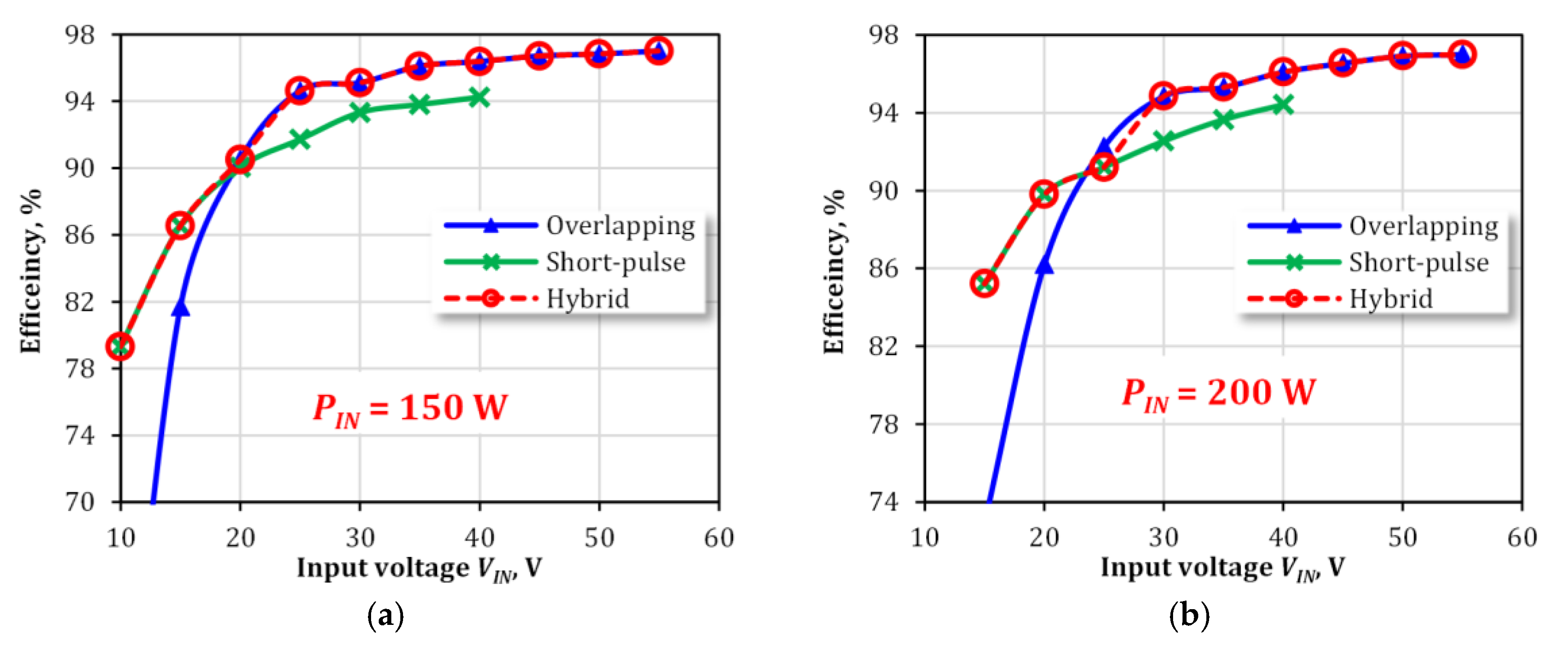
Nevertheless, the overlapping PWM scheme provides the lowest losses in the converter compared to the short-pulse scheme but only in the normal operating conditions. Therefore, the proposed hybrid PWM corresponds to using the overlapping modulation in the normal operating conditions and the proposed short-pulse PWM scheme in the abnormal operating conditions. This can keep the converter at a high level in a wide input voltage range.

4. Experimental Results

4.1. Description of the Experimental Setup

To validate the proposed hybrid PWM scheme, a 300 W prototype was assembled and tested in the laboratory as shown in Figure 9. The list of the prototype parameters and components is given in Table 1. The converter is designed to generate the output voltage of 350 V without any boosting interval, i.e., Db = 0, at the input voltage of 60 V. Therefore, the transformer turns ratio is selected equal to 6. The input voltage range of 15 V to 60 V suits well for the photovoltaic module-level applications. The implementation of the control system and the generation of the modulation sequences were performed using a low-cost STM32F334 microprocessor (STMicroelectronics, Geneva, Switzerland). Also, all the efficiency values were recorded using an 1800WT power analyzer (Yokogawa, Tokyo, Japan). The measured efficiency does not include the auxiliary power supply losses in the converter. The designed transformer has a low leakage inductance so an external inductor was added to increase the leakage inductance, and consequently, improve the efficiency as stated earlier. The low leakage inductance value is achieved by interleaved winding construction where three layers of the secondary winding connected in series are separated by two layers fo the primary winding connected in parallel. This design limits leakage flux magnitude and consequently minimizes ac resistance of the transformer windings. Accordingly, the total value of the resonant inductance equals 97 µH. With the utilized resonant tank parameters, the resonant frequency is 94 kHz, which is close to the switching frequency according to the efficiency considerations.

4.2. Steady-State Waveforms

The waveform of the overlapping and proposed schemes at a power level of 300 W at the same input voltage of 25 V is given in Figure 10 and Figure 11, respectively. The primary current with the overlapping modulation crosses the zero axes and flows in the reverse direction while the primary voltage does not change, see Figure 10a. However, with the proposed short-pulse PWM shown in Figure 10a, the converter operates in the discontinuous conduction mode when the inductor current stays unchanged till the end of each half-cycle after it reaches zero value. During these zero-current time intervals, the converter experiences parasitic oscillations between the leakage inductance and the parasitic capacitances fo the output side semiconductor devices. Comparing Figure 10 and Figure 11 it could be concluded that in the abnormal operating conditions, the converter suffers from additional circulating currents, and consequently, from the increased voltage stress of the resonant capacitor, all of which would result in deteriorated efficiency.
The experimental waveforms at a higher input voltage of 45 V with the same power level at 300 W for the overlapping PWM scheme are shown in Figure 12. This case represents the normal operation of the SRC with the overlapping modulation at Δ V C r < 2 n V I N , where the abnormal operating conditions do not exist. Also, the experimental and theoretical values of Δ V C r are 190 V and 195 V, respectively, in the operating point presented in Figure 12. It is worth mentioning the similarity between Figure 11 and Figure 12, which proves the assumption that the short-pulse PWM scheme does not change the fundamental principle of the converter operations, but instead allows avoiding the abnormal operating conditions.

4.3. Determining of Optimal Transition between PWM Schemes

The input voltage and the current of the converter have to be sensed to identify in which region the converter is operating and select the best PWM scheme at each operating point for the best efficiency. The target operating range of the converter is limited by the minimum input voltage of 10 V, the maximum input current of 15 A, and the maximum input power of 300 W. The envelope of the target operating range is shown along with the theoretical and experimental borderline defining the optimal modulation scheme are shown in Figure 13. The experimental borderline lies higher than the theoretical one due to the influence of the converter power loss, as it takes more input power in practice to reach the abnormal operating conditions at the same voltage. The converter will experience abnormal operating conditions on the left from the borderline if the overlapping PWM scheme is used. Therefore, the proposed short-pulse PWM scheme has to be used on the left from the borderline, which significantly extends the input voltage operating range compared to the overlapping PWM scheme. The experimental borderline was defined by applying the overlapping PWM scheme and keeping the input voltage constant when the input power is adjusted by changing the resistive load. At the same time, the drain-source voltages of MOSFETs Q1 or Q2 were observed to identify when the current starts flowing through the body diodes these MOSFETs.
The experimental borderline could be approximately fitted by a quadratic equation describing the input power PIN as a polynomial function of the input voltage VIN:
P I N ( b o r d e r l i n e ) = 0.36 · V I N 2 2.1 · V I N ,
which yields a very high coefficient of determination (R2) of 0.998. From the relation between the input power and the input voltage, the critical value of the input current Icri can be calculated to define at which operating point the conventional overlapping PWM scheme has to be changed to the proposed short-pulse PWM scheme, as indicated in Figure 13. It could be obtained from Equation (17):
I c r i = 0.36 · V I N 2.1 .
A simplified block diagram that describes the implementation of the proposed hybrid PWM scheme is given in Figure 14. The main criteria to switch between the overlapped and the short-pulse modulation schemes is the value of the input current IIN of the converter compared to the critical current Icri at the corresponding input voltage VIN, which is defined by Equation (18). When IIN is larger than Icri, the abnormal operating condition is expected to appear, and thus, the converter should operate with the proposed short-pulse PWM scheme. Otherwise, the converter can operate with the overlapped modulation at the highest efficiency outside the abnormal conditions. The empirical threshold between the two modulation schemes corresponds to the red line in Figure 13.
The transition between the PWM schemes within implemented within a closed-loop control system based on a typical proportional-integral (PI) controller has been tested in two scenarios as follows:
  • Load step-change: The input voltage is kept constant during this test at 20 V. When the step change is applied, the PWM scheme is changed automatically in Figure 15a where the yellow signal indicates to the PWM type. When this signal is high, the short-pulse PWM scheme is applied. It is applied at higher power because the peak-to-peak ripple of the resonant capacitor voltage is larger than the voltage of the transformer secondary winding.
2.
Input voltage ramp-change: The input voltage is changed from 50 V to 15 V as a linearly decreasing ramp with a duration of 0.5 s, while the load resistance is constant. This voltage change must trigger a transition between two PWM schemes as shown in Figure 13. The input power during this test is above 100 W at any voltage tested, but it does not exceed 150 W to avoid triggering the overcurrent protection during regulation transients. The converter operation with the selected input voltage ramp is presented in Figure 15b. The output voltage remains constant during the input voltage decreasing as a PI controller adjusts the converter duty-cycle. The input current disturbances were observed: one event is related to the change of the PWM scheme and associated change in the operation of the resonant capacitor, the other disturbance happens at the end of the voltage ramp resulting from the I-component overshoot of the PI controller.

4.4. Efficiency Evaluation

The measured efficiencies of the studied converter with the original overlapping and the proposed short-pulse PWM schemes versus the power level are given in Figure 16 at three input voltages of 15, 20 and 50 V, i.e., four-fold, three-fold, and nearly unity input voltage step-up, respectively. In the figure, the blue lines correspond to the conventional PWM scheme with overlapping control signals, the green lines represent the proposed short-pulse PWM scheme, while the red dashed line represents their envelope that corresponds to the proposed hybrid modulation that benefits from switching between these two modulations. The intersection of the green and blue lines in each figure represents the boundary point at which the capacitor voltage equal to the secondary winding voltage. The power value at the intersection point is different in Figure 16a,b because the input voltage is different in these cases, which agrees with the Equations (3) and (17). The proposed short-pulse PWM scheme demonstrates efficiency improvement by 13% when compared to that of the overlapping PWM scheme at the input voltage of 15 V and the load power of 225 W (at the maximum input current). Consequently, the proposed hybrid modulation can harness the advantages of each of the two basic PWM scheme in the corresponding operating regions of their best performance. It is worth mentioning that at low voltage step-up values, i.e., in the case of VIN = 50 V shown in Figure 16c, the conventional overlapping PWM scheme is the best choice and the application of the short-pulse PWM scheme is not needed, as was described in Figure 13. Moreover, Figure 17 describes how the converter efficiency could be improved by employing the hybrid PWM scheme in the cased of converter operation at a fixed input power and variable input voltage. It can be seen that the hybrid PWM scheme employs the short-pulse PWM at lower input voltages to achieve a significant increase in the converter efficiency. Otherwise, the abnormal operating conditions with high losses in the components would have appeared at the lower input voltages due to the use of the overlapping PWM scheme.

4.5. Evaluation of DC Voltage Gain with Short-Pulse PWM Scheme

The proposed short-pulse PWM scheme is expected to follow the same relation between the converter DC voltage gain, which refers to the ratio between the output voltage and the input voltage, and the cumulative boosting duty cycle Db. This relation is described in Equation (16), which is applicable to the short-pulse PWM scheme at any operating point. However, its applicability to the overlapping PWM scheme is limited to the range of the normal operating conditions. Figure 18 presents a comparison between the theoretical Equation (16) depicted with a line and experimental duty cycle values for both the basic PWM scheme depicted with dots. Two values of the constant input power were selected for the tests as the converter can operate in a wide input voltage range at these power levels as shown in Figure 13. At the same time, their theoretical DC voltage gain curves are different enough to perform the comparison. It is worth mentioning, that experimental duty cycle values that correspond to the use of the overlapping PWM scheme in the abnormal operating conditions are excluded from the plots. As a result, the use of the overlapping PWM scheme is limited to the DC voltage gain values below twenty at PIN = 150 W, and below fifteen at PIN = 200 W to avoid the abnormal operating conditions. At higher values of the DC voltage gain, the short-pulse PWM scheme was used. In this way, the hybrid PWM scheme avoids excessive power losses associated with the abnormal operating conditions and makes this converter suitable for applications with a wide input voltage range. The experimental data follow the theoretical gain curve tightly at lower DC voltage gain values. More considerable differences occur at DC voltage gain values of over twenty, which is related to the converter operation at low input voltages and relatively high converter power loss even with the short-pulse PWM scheme, which were not considered in the theoretical analysis. As expected from Equation (16), the input power affects the duty cycle value at the same DC voltage gain. For example, when the converter operates at the DC voltage gain of twenty, Db equals 0.42 and 0.48 at the input power of 150 W (Figure 18a) and 200 W (Figure 18b), respectively.

5. Conclusions

The paper analyses operation of the series resonant DC-DC converter with the bridgeless boost rectifier in a wide input voltage range. It was shown that this converter experiences abnormal operating conditions at high DC voltage gain values, when the converter suffers from large circulating currents and, consequently, high power losses. This effect results from the use of the conventional overlapping PWM scheme in a wide input voltage range. To avoid the operation of the converter in the abnormal conditions, it was proposed to replace the conventional PWM scheme, where the duty cycle of the rectifier switches is over 0.5, with the short-pulse PWM scheme, where the duty cycle of the rectifier switches is reduced to the actual duration of the voltage boosting time intervals, where needed. In this way, the hybrid PWM scheme was introduced, which employes one of the two basic PWM schemes with the best efficiency at any operating point. The borderline between the two PWM schemes was defined experimentally and fitted with a second-order polynomial function, which enabled simple implementation of the closed-loop control system. Smooth transition between the two PWM schemes could be achieved as their boosting duty cycles follows the same theoretical law describing their dependence on the input voltage and power. This was verified experimentally when considering only normal operating conditions for the overlapping PWM scheme.
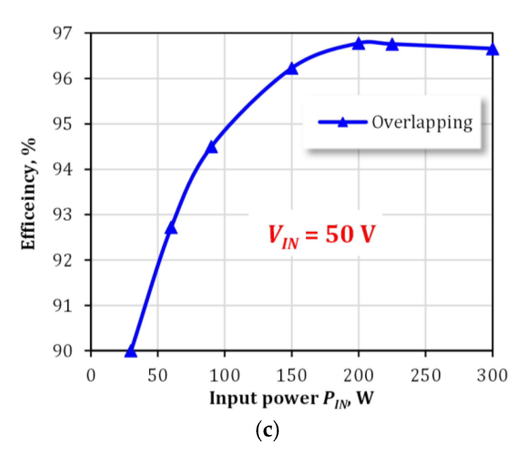
Hence, the logic defining the transition between the two PWM schemes was implemented with simple calculations and comparison operations, which could be decoupled from the main control loop. As a result, significant efficiency improvement of over 10% was achieved at low input voltages and relatively high input currents, where the short-pulse PWM scheme is employed. The peak converter efficiency of 97.1% was recorded near the minimum DC voltage gain. The converter demonstrated a nearly sixfold range of the DC voltage gain experimentally, which is a remarkable result considering that only the input voltage boost operation was considered. Future research will be focused on optimization of the converter components for operation in a wide input voltage and current range to improve the converter peak and average efficiency.

Author Contributions

Conceptualization, A.B. and A.C.; methodology, A.B.; software, A.B.; validation, A.R. and A.B.; formal analysis, A.C. and A.B.; investigation, A.B.; resources, D.V. and A.R.; data curation, A.C. and A.R.; writing—original draft preparation, A.C. and A.B.; writing—review and editing, A.C., A.R., and D.V.; visualization, A.C. and A.B.; supervision, A.C. and D.V.; project administration, A.C.; funding acquisition, A.C. and A.R. All authors have read and agreed to the published version of the manuscript.

Funding

This work has been supported in part by the European Commission through the H2020 project Finest Twins (grant No. 856602), in part by the Estonian Research Council grant PSG206, and in part by the Estonian Centre of Excellence in Zero Energy and Resource Efficient Smart Buildings and Districts, ZEBE, grant 2014-2020.4.01.15-0016 funded by the European Regional Development Fund.

Conflicts of Interest

The authors declare no conflict of interest.

References

  1. Kavlak, G.; McNerney, J.; Trancik, J.E. Evaluating the Causes of Cost Reduction in Photovoltaic Modules. Energy Policy 2018, 123, 700–710. [Google Scholar] [CrossRef] [Green Version]
  2. Shukla, A.K.; Sudhakar, K.; Baredar, P. Recent Advancement in BIPV Product Technologies: A Review. Energy Build. 2017, 140, 188–195. [Google Scholar] [CrossRef]
  3. Sorgato, M.J.; Schneider, K.; Rüther, R. Technical and Economic Evaluation of Thin-Film CdTe Building-Integrated Photovoltaics (BIPV) Replacing Façade and Rooftop Materials in Office Buildings in a Warm and Sunny Climate. Renew. Energy 2018, 118, 84–98. [Google Scholar] [CrossRef]
  4. Biyik, E.; Araz, M.; Hepbasli, A.; Shahrestani, M.; Yao, R.; Shao, L.; Essah, E.; Oliveira, A.C.; del Caño, T.; Rico, E.; et al. A Key Review of Building Integrated Photovoltaic (BIPV) Systems. Eng. Sci. Technol. Int. J. 2017, 20, 833–858. [Google Scholar] [CrossRef]
  5. Sechilariu, M.; Locment, F.; Wang, B. Photovoltaic Electricity for Sustainable Building. Efficiency and Energy Cost Reduction for Isolated DC Microgrid. Energies 2015, 8, 7945–7967. [Google Scholar] [CrossRef] [Green Version]
  6. Batarseh, I.; Alluhaybi, K. Emerging Opportunities in Distributed Power Electronics and Battery Integration: Setting the Stage for an Energy Storage Revolution. IEEE Power Electron. Mag. 2020, 7, 22–32. [Google Scholar] [CrossRef]
  7. Vinnikov, D.; Chub, A.; Liivik, E.; Roasto, I. High-Performance Quasi-Z-Source Series Resonant DC–DC Converter for Photovoltaic Module-Level Power Electronics Applications. IEEE Trans. Power Electron. 2017, 32, 3634–3650. [Google Scholar] [CrossRef]
  8. Chub, A.; Vinnikov, D.; Lai, J.-S. Input Voltage Range Extension Methods in the Series-Resonant DC-DC Converters. In Proceedings of the 2019 IEEE 15th Brazilian Power Electronics Conference and 5th IEEE Southern Power Electronics Conference (COBEP/SPEC), Sao Paulo, Brazil, 1–4 December 2019; IEEE: Piscataway, NJ, USA, 2019. [Google Scholar] [CrossRef]
  9. Singh, Y.V.; Viswanathan, K.; Naik, R.; Sabate, J.A.; Lai, R. Analysis and Control of Phase-Shifted Series Resonant Converter Operating in Discontinuous Mode. In Proceedings of the 2013 Twenty-Eighth Annual IEEE Applied Power Electronics Conference and Exposition (APEC), Long Beach, CA, USA, 17–21 March 2013; IEEE: Piscataway, NJ, USA, 2013. [Google Scholar] [CrossRef]
  10. Kim, E.H.; Kwon, B.H. Zero-Voltage- and Zero-Current-Switching Full-Bridge Converter with Secondary Resonance. IEEE Trans. Ind. Electron. 2010, 57, 1017–1025. [Google Scholar] [CrossRef]
  11. Zhao, X.; Zhang, L.; Born, R.; Lai, J.-S. A High-Efficiency Hybrid Resonant Converter with Wide-Input Regulation for Photovoltaic Applications. IEEE Trans. Ind. Electron. 2017, 64, 3684–3695. [Google Scholar] [CrossRef]
  12. Kim, J.-W.; Park, M.-H.; Han, J.-K.; Lee, M.; Lai, J.-S. PWM Resonant Converter with Asymmetric Modulation for ZVS Active Voltage Doubler Rectifier and Forced Half Resonance in PV Application. IEEE Trans. Power Electron. 2020, 35, 508–521. [Google Scholar] [CrossRef]
  13. Wu, H.; Zhang, J.; Qin, X.; Mu, T.; Xing, Y. Secondary-Side-Regulated Soft-Switching Full-Bridge Three-Port Converter Based on Bridgeless Boost Rectifier and Bidirectional Converter For Multiple Energy Interface. IEEE Trans. Power Electron. 2015, 31, 4847–4860. [Google Scholar] [CrossRef]
  14. Son, S.; Montes, O.A.; Junyent-Ferre, A.; Kim, M. High Step-Up Resonant DC/DC Converter with Balanced Capacitor Voltage for Distributed Generation Systems. IEEE Trans. Power Electron. 2019, 34, 4375–4387. [Google Scholar] [CrossRef]
  15. Zhao, X.; Chen, C.-W.; Lai, J.-S. A High-Efficiency Active-Boost-Rectifier-Based Converter with a Novel Double-Pulse Duty Cycle Modulation for PV to DC Microgrid Applications. IEEE Trans. Power Electron. 2019, 34, 7462–7473. [Google Scholar] [CrossRef]
  16. LaBella, T.; Yu, W.; Lai, J.-S.; Senesky, M.; Anderson, D. A Bidirectional-Switch-Based Wide-Input Range High-Efficiency Isolated Resonant Converter for Photovoltaic Applications. IEEE Trans. Power Electron. 2014, 29, 3473–3484. [Google Scholar] [CrossRef]
  17. Shen, Y.; Wang, H.; Qin, Z.; Blaabjerg, F.; Durra, A.A. A Reconfigurable Series Resonant DC-DC Converter for Wide-Input and Wide-Output Voltages. In Proceedings of the 2017 IEEE Applied Power Electronics Conference and Exposition (APEC), Tampa, FL, USA, 26–30 March 2017; IEEE: Piscataway, NJ, USA, 2017. [Google Scholar] [CrossRef]
  18. Huber, L.; Jang, Y.; Jovanovic, M.M. Performance Evaluation of Bridgeless PFC Boost Rectifiers. IEEE Trans. Power Electron. 2008, 23, 1381–1390. [Google Scholar] [CrossRef]
  19. Musavi, F.; Edington, M.; Eberle, W.; Dunford, W.G. Energy Efficiency in Plug-in Hybrid Electric Vehicle Chargers: Evaluation and Comparison of Front End AC-DC Topologies. In 2011 IEEE Energy Conversion Congress and Exposition; IEEE: Piscataway, NJ, USA, 2011. [Google Scholar] [CrossRef]
Figure 1. SRC converter based on the bridgeless rectifier in the output-side [11].
Energies 13 04220 g001
Figure 2. Idealized steady-state waveform of the bridgeless converter for the abnormal operating conditions when Δ V C r > 2 n V I N .
Energies 13 04220 g002
Figure 3. Sketch of the state-plane trajectory of the resonant tank with the overlapping PWM scheme for the abnormal operating conditions when Δ V C r > 2 n V I N .
Energies 13 04220 g003
Figure 4. Operating modes of the converter during a one-half cycle with the overlapping modulation at Δ V C r > 2 n V I N : (a) Mode I; (b) Mode II; (c) Mode III.
Energies 13 04220 g004
Figure 5. Equivalent circuits of the converter during the one-half cycle with the overlapping modulation at Δ V C r > 2 n V I N : (a) Mode I; (b) Mode II; (c) Mode III.
Energies 13 04220 g005
Figure 6. Idealized steady-state waveform with the proposed short-pulse PWM scheme for Δ V C r > 2 n V I N .
Energies 13 04220 g006
Figure 7. State-plane trajectory of the resonant tank with the proposed short-pulse PWM for Δ V C r > 2 n V I N .
Energies 13 04220 g007
Figure 8. Operating modes of the converter during a one-half cycle with the short-pulse modulation: (a) Mode I; (b) Mode II; (c) Mode III.
Energies 13 04220 g008
Figure 9. Photo of the experimental prototype.
Energies 13 04220 g009
Figure 10. Waveforms of the studied topology with the overlapping PWM at PIN = 300 W and VIN = 25 V: (a) front-end inverter; (b) bridgeless rectifier; (c) output and resonant capacitor voltage.
Energies 13 04220 g010
Figure 11. Waveforms of the studied topology with the proposed short-pulse PWM at PIN =300 W and VIN = 25 V: (a) front-end inverter; (b) bridgeless rectifier; (c) output and resonant capacitor voltage.
Energies 13 04220 g011
Figure 12. Waveforms of the studied topology with the overlapping PWM at PIN = 300 W and VIN = 45 V: (a) front-end inverter; (b) bridgeless rectifier; (c) output and resonant capacitor voltage.
Energies 13 04220 g012
Figure 13. Locations of the experimental and theoretical borderlines describing the transition between the overlapping and the short-pulse PWM schemes employed in the hybrid PWM scheme within the target operating range.
Energies 13 04220 g013
Figure 14. Block diagram describing the implementation of transitions between the two PWM schemes based on the empiric Equation (18).
Energies 13 04220 g014
Figure 15. The converter operation with a closed-loop control system in the cases of: (a) a load step-change; (b) an input voltage ramp-change.
Energies 13 04220 g015
Figure 16. Experimental efficiency versus the converter power at fixed input voltages: (a) VIN = 15 V; (b) VIN = 20 V; (c) VIN = 50 V.
Energies 13 04220 g016aEnergies 13 04220 g016b
Figure 17. Experimental efficiency dependence on the input voltage for different PWM schemes evaluated at fixed input power values: (a) PIN = 150 W; (b) PIN = 200 W.
Energies 13 04220 g017
Figure 18. Comparison between the theoretical DC voltage gain and the experimental data at two input power values: (a) PIN = 150 W; (b) PIN = 200 W.
Energies 13 04220 g018
Table 1. Experimental setup parameters and components.
Parameter/ComponentSymbolValue/Part Number
Input voltage rangeVIN10–60 V
Maximum input current15 A
Output voltageVOUT350 V
Switching frequencyFSW95 kHz
Input side capacitorCIN150 µF
Primary side switchesS1–4FDMS86180
Transformer leakage inductance Llk4 µH
Transformer magnetizing inductanceLm1.3 mH
External inductorLext93 µH
Transformer core materialTXFerrite 3C95
Transformer core geometryETD39
Primary turns9 (Litz wire)
Secondary turns54 (Litz wire)
External inductor core materialLextFerrite 3C95
External inductor core geometryE42
External inductor turns33 (Litz wire)
External inductor core air gap11 mm
Resonance capacitorCr30 nF, Film type
Bridgeless rectifier MOSFETs Q1, Q2SCT2120AF
Bridegless rectifier diodesD1, D2C3D02060E
Output-side capacitorsCO150 µF

