Article

Emerging Photovoltaic (PV) Materials for a Low Carbon Economy

1
Sustainability and Renewable Energy Systems Program, Department of Electrical and Computer Engineering, University of Wisconsin-Platteville, Platteville, WI 53818, USA
2
Wright Center for Photovoltaics Innovation and Commercialization, Department of Physics and Astronomy, The University of Toledo, Toledo, OH 43606, USA
3
Department of Civil and Environmental Engineering, The University of Toledo, Toledo, OH 43606, USA
*
Author to whom correspondence should be addressed.
Energies 2020, 13(16), 4131; https://doi.org/10.3390/en13164131
Submission received: 2 July 2020 / Revised: 3 August 2020 / Accepted: 7 August 2020 / Published: 10 August 2020
(This article belongs to the Special Issue Perovskite Solar Cells)

Abstract

:
Emerging photovoltaic (PV) technologies have a potential to address the shortcomings of today’s energy market which heavily depends on the use of fossil fuels for electricity generation. We created inventories that offer insights into the environmental impacts and cost of all the materials used in emerging PV technologies, including perovskites, polymers, Cu2ZnSnS4 (CZTS), carbon nanotubes (CNT), and quantum dots. The results show that the CO2 emissions associated with the absorber layers are much less than the CO2 emissions associated with the contact and charge selective layers. The CdS (charge selective layer) and ITO (contact layer) have the highest environmental impacts compared to Al2O3, CuI, CuSCN, MoO3, NiO, poly (3-hexylthiophene-2,5-diyl (P3HT)), phenyl-C61-butyric acid methyl ester (PCBM), poly polystyrene sulfonate (PEDOT:PSS), SnO2, spiro-OMeTAD, and TiO2 (charge selective layers) and Al, Ag, Cu, FTO, Mo, ZnO:In, and ZnO/ZnO:Al (contact layers). The cost assessments show that the organic materials, such as polymer absorbers, CNT, P3HT and spiro-OMeTAD, are the most expensive materials. Inorganic materials would be more preferable to lower the cost of solar cells. All the remaining materials have a potential to be used in the commercial PV market. Finally, we analyzed the cost of PV materials based on their material intensity and CO2 emissions, and concluded that the perovskite absorber will be the most eco-efficient material that has the lowest cost and CO2 emissions.

Graphical Abstract

1. Introduction

Todays’ global power consumption is ~6 TW [1] and is expected to triple to 18 TW [2,3] by 2050, with a projected increase in the global energy demand of 1.1 GW/day from 2020 and 2050. To meet this challenge, an average nuclear power plant would need to build each day of the next 30 years (globally) [4] at the cost of 1.6 to 2.7 billion USD each day [5]. The World Energy Council forecasts that the low-carbon energy sources tackling the mitigation of climate change will play a central role in addressing this challenge and solar photovoltaic (PV) materials will be the major driver in the coming renewable energy market [5,6].
Today, the global installed capacity of solar PV is about 480 GW [7] with >90% of this capacity utilizing wafer-based crystalline silicon (c-Si) technology. c-Si technology is fabricated on semiconducting wafers and can be built without an additional substrate, although modules are typically covered with glass for mechanical stability and protection [8,9] and 8 to 9% of the solar PV market is thin film technology [10]. Thin film cells consist of semiconducting films deposited onto a glass, plastic, or metal substrate. There is a limitation of the large scale global market penetration of these technologies due to production costs, material availability, and slow manufacturing [4,11].
Several new PV technologies have emerged to overcome these limitations [12,13]. They are methylammonium lead halide perovskites [14] (CH3NH3PbX3, where X = I, Br, or Cl), polymers, Cu2ZnSnS4 (CZTS), carbon nanotubes (CNTs) and quantum dots (Figure 1a). All of these emerging technologies have the same basic device structure (Figure 1b), with the absorber as the middle layer in contact with two charge selective layers (electron and hole transports) and contacts (front and back) at the edges. In this structure, the light is transmitted into the absorber layer and excites electrons and holes. Electrons and holes flow into their respective selective layers before continuing contact, thereby creating a current, which generates power set to an operating voltage. There are a number of materials that can be used as charge selective and contacting layers (Figure 1b), most of which are relatively new and purposely optimized to be used in the emerging PVs.
Despite the clear interest in analyzing the environmental and economic impacts of emerging materials used in these technologies [14,15,16,17,18,19,20,21], the detailed inventories used in these devices have largely been overlooked. This has led to each group using a unique set of assumptions that make the results difficult to compare. For example, Gong et al. found the total CO2 emissions from a perovskite device structure as ~22 g/kWh [22], while Espinosa (2015) et al. reported a value of 2700 g/kWh [23]. The CO2 emissions from fabricating only the perovskite component of the devices also varies ~28 times between these studies as, with the environmental assessments, the economic analysis on perovskite devices was found to vary from 3- to 4-fold (30 USD to 140 USD) [24,25,26]. While the cost and environmental impacts of perovskite PVs have been analyzed many times by various researchers in different device structures, other emerging PVs have not been explored in detail.
In this study, we created a large set of inventories that offer insights into the environmental impacts and cost of all the materials used in emerging PV technologies, using consistent assumptions for commercial scale manufacturing. This question was addressed by assessing the CO2 emissions and cost of each alternative layer. The assessments reflect the effect of materials and their processing techniques on the device’s economic and environmental performances. Similarly, the alternative absorber layers were investigated to inform the decisions-makers regarding which emerging technologies should enter the commercial market. Finally, an eco-efficiency concept that incorporates the environmental impacts and cost of materials was developed to promote an eco-design perspective for emerging PV materials.

2. Methods

2.1. Life Cycle Inventories

We prepared the inventories for the life cycle inventories of the alternative layer-using PV cells (Figure 1). These materials are shown as promising for commercial production since either they offer a low cost production or highly efficient solar modules. For example, inorganic materials, such as NiO, CuSCN, SnO2, MoO3 and ZnO, are low-cost materials that have shown high efficiencies (>20%) in perovskite PV cells. Other inorganic materials such as CdS and TiO2 materials have been already used in commercial thin film technologies. Particularly, CdS could be a low-cost charge selective for CZTS PVs. Al2O3 has been assessed in quantum dot PVs that can reach a 12% power conversion efficiency. Organic materials such as poly (3-hexylthiophene-2,5-diyl (P3HT)), poly polystyrene sulfonate (PEDOT:PSS), phenyl-C61-butyric acid methyl ester (PCBM) and Sprio-OMeTAD have been analyzed in polymer and perovskite (CH3NH3PbX3, where X = I, Br, or Cl) materials. Indeed, these organic materials were used for the flexible polymer solar modules manufactured mid-scale by the Technical University of Denmark. Al, Ag, FTO, and ITO layers have been studied in all emerging PV technologies, while Al and FTO materials have been already used by PV industry.
The energy inventories for the depositions of the materials were modeled. Table 1 lists the methods used for the deposition of each layer. These deposition techniques are the most commonly used methods in fabricating emerging PVs (extracted from the literature). Note that among these methods, doctor blading, printing, and spinning are solution-based methods and they can be used interchangeably between the layers. Sputtering and evaporation are thermal methods that are used in the PV market. The electricity consumption of these methods was scaled up for large scale manufacturing. These efforts were built on the University of Toledo Photovoltaic Innovation Center (PVIC)’s experiences in manufacturing these cells in lab scale. All the deposition methods given in Table 1 are used at PVIC labs. The estimation incorporates the time and power required for the deposition, pumping, and annealing of each material.
The life cycle inventories for each layer component was built using GaBi 8.0 software. The data for CdSe quantum dots, P3HT, CuI, and Al2O3 were created using literature data [27,28], while the remaining inventories were taken from our group’s previous studies [10,29,30,31].

2.2. Cost Assessment

The cost data for the assessment model include the PV materials and their depositions on the device structure were calculated (Figure 2). The raw cost data for the inventories were taken from our group’s previous publication [32]. For the materials, there is little publicly available information on the costs and prices from PV companies. The assumptions and cost data were created using the literature and online sources, including global trading websites, as well as reports from governments and other organizations. Some of the data were directly extracted from our group’s previous publication [26]. For the manufacturing cost, the processing time, degree of automation for each step and the US electricity price were used.

3. Results

3.1. Life Cycle Carbon Emissions

The GWP of the absorber materials varied ~2–52 g CO2/m2. These values are three to four orders of magnitude smaller than the GWPs of the c-Si, CdTe and CIGS absorber materials commonly used in today’s commercial market [33]. Among the absorber materials, CdSe quantum dot materials have the highest GWP value (51.54 g CO2/m2). The reasons for these high GWP values almost equally contribute to the use of electricity (52%) and materials (48%). The electricity is utilized in the deposition of thin films of CdSe quantum dots while different chemicals are used during the synthesizing, isolation and purifying of the quantum dots. The butanol (~24%) and methanol (20%) that were consumed during the steps of preparation of quantum dot nanomaterials dominate the GWP emissions associated with the materials. CZTS has the second highest GWP value. The high GWP value of the CZTS layer is due to the electricity consumption used for CZTS depositions. CZTS is the thickest absorber layer among the alternatives (2000 nm) studied here. Thus, despite the solution-based methods used in deposition (spinning, annealing), the CO2 emissions due to electricity consumption (4.89 MJ/m2) contribute to the high GWP impact. CNTs, perovskite (CH3NH3PbX3, where X = I, Br, or Cl) and polymers (mixture of PCBM and P3HT) have low GWP values. For all of these absorber layers, chemicals used in material synthesis dominate the GWP values. The most impactful chemicals used in the preparation of perovskite, polymer, and CNT absorber materials are dimethylformamide (84% of the total impacts), ultrapure water (37%) and carbon monoxide (90%), respectively.
The GWP of the alternative charge selective layers varied by a factor of ~300. CdS has the largest value for CO2 emissions among all the alternatives. The reason for such a high impact is mainly the plasma-enhanced chemical vapor deposition (PECVD) method in preparing CdS. This deposition technique has been used in the manufacturing processes of CdTe technology. Among inorganic charge selective materials, such as NiO, SnO2, CuSCN, MoO3 and TiO2, NiO has the highest GWP value while TiO2 has the lowest. For both of these layers, the electricity required for deposition is the main contributor. However, the difference between electricity consumption is due to a deposition time which is ~20 times longer for NiO compared to TiO2 (Table 2). Similar to inorganic charge selective materials, the organic transport layers have low GWP values. All of these organic materials are deposited by solution-based methods. Among the four alternatives, spiro-OMeTAD was found to have the lowest GWP (50 g CO2 per m2) charge selective option.
The GWP of contact materials varied by several times (from ~100 g CO2/m2 for Al to ~15 kg CO2/m2 for ITO). A high GWP of ITO was reported in the literature [34,35]. Many studies showed that ITO is the most impactful component of the device when it is used as a back-contact of perovskite [22], polymer [34] and CNT [29] solar cells. ITO material is deposited by the sputtering method. Thin films of Mo, ZnO:In and ZnO/ZnO:Al are also deposited by a sputtering method. The main difference for lower GWP values compared to ITO is attributed to the differences in the time required for pumping the sputtering chamber and for the deposition of material.
The GWP results show that CO2 emissions resulting from one of the back-contact materials (ITO) and three of the charge selective (CdS, ZnO:In, and ZnO:ZnO-Al) materials are several times higher than those of the emissions from absorber materials.

3.2. Life Cycle Costing

Figure 3 shows the cost of the materials used in emerging PV technologies. CNTs and polymer absorbers were found to be the most expensive materials. Despite the multiple required steps for synthesizing the CdSe QD nanomaterials, they are not the most expensive option. CZTS and perovskite are the most promising materials due to their low cost.
Similar to absorber materials, the material cost of charge selective materials has a large range. Organic materials such as spiro-OMeTAD and PCBM are the most expensive charge selective alternatives. The cost of P3HT and PEDOT:PSS are relatively lower than other organics since they have been used in the solar industry for a longer time, and as such, their costs have reduced. As it is seen, all the other inorganic materials are much cheaper, and as such, are estimated to be more favorable alternatives than organic materials for commercial production.
Except Ag and ITO, the costs of all contact materials are less than 10 cent/m2. Note that, despite the high cost, Ag is commercially used in c-Si technology. Similarly, ITO material is also used in commercial markets in smart phones and in the windows of planes. Therefore, it may be concluded that all the assessed contact materials may potentially play a role in the future PV market.

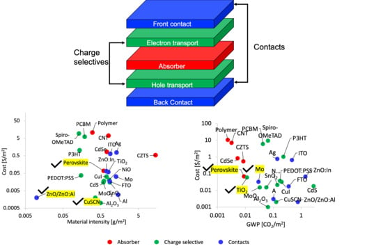
3.3. Low-Cost and Eco-Efficient Material Selection for Emerging PVs

Low-cost and eco-efficient materials for emerging PVs are shown in Figure 4a,b. Figure 4a shows that the choice of ZnO:ZnO:Al is the most ideal from the perpective of cost and material intensity. This material ranks the lowest at both metrics among charge selective layers. It is also shown that the polymer and CNT absorbers and spiro-OMeTAD, and PCBM charge selective materials have the highest cost per unit mass of material used; thus, these materials are not suitable for low-cost energy productions from photovoltaic systems with their current cost. Among all the materials assessed, we found perovskite and ZnO/ZnO:Al as the lowest-cost absorber and contacting materials. The cost of the charge selective materials CuSCN and Al2O3 were found to be very similar to each other and the orders of magnitude were lower compared to other contacting materials such as P3HT, spiro-OMeTAD and PCBM. Other charge selective layers, such as CdS, CuI, SnO2, were ranked intermediate in cost, while all inorganic options for the charge selective layers showed similar material intensity.
Figure 4b shows that the cost of PV materials compared to their GWP impacts. The materials that have a high cost but low GWP [36] are polymer and CNT absorbers, as well as spiro-OMeTAD and PCBM charge selective materials, while the options with a low cost but high GWP are CdS, ITO, ZnO:In, and ZnO:ZnO:Al. Among all the investigated materials, perovskite absorbers were found to be the most eco-efficient material that has the lowest cost and relatively low GWP impacts while Mo and TiO2 were found to be the most eco-efficient contacting and charge selective materials.

4. Conclusions

In this study, we aimed to create inventories that offer insights into the environmental impacts and cost of all the materials used in emerging PV technologies. The results show that CO2 emissions from the absorber layers are much less than the CO2 emissions from contact and charge selective layers. CdS and ITO are the highest impact charge selective and contact materials, respectively. The cost assessments showed that the organic materials, such as polymer absorbers, CNTs, P3HT, PCBM and spiro-OMeTAD, are the most expensive materials. All the remaining materials have a potential to be used in the commercial PV market. Finally, we analyzed the cost of PV materials based on their material intensity and CO2 emissions, and concluded that perovskite absorbers will be the most eco-efficient material which has the lowest cost and GWP impacts.

Author Contributions

Conceptualization, I.C., R.H.A. and D.A.; methodology, I.C., Z.S.; software, I.C.; validation, I.C., R.H.A.; formal analysis, I.C.; investigation, I.C. and R.H.A., data curation, I.C. and R.H.A.; writing—original draft preparation, I.C.; writing—review and editing, R.H.A., Z.S., M.H., and D.A., funding acquisition, M.H. and D.A. All authors have read and agreed to the published version of the manuscript.

Funding

This research was funded by the National Science Foundation CHE-1230246 & ECCS-1665172 and the Helen and Harold McMaster Endowment for Photovoltaics.

Conflicts of Interest

The authors declare no conflict of interest.

References

  1. Enerdata. Global Energy Statical Yearbook. 2019. Available online: https://www.enerdata.net/about-us/company-news/energy-statistical-yearbook-updated.html (accessed on 8 August 2020).
  2. Hostick, D.; Belzer, D.; Hadley, S.; Markel, T.; Marnay, C. Projecting Electricity Demand in 2050; PNNL: Richland, WA, USA, 2014. [Google Scholar]
  3. U.S. EIA Annual Energy Outlook 2019 with projections to 2050. Annu. Energy Outlook 2019 Proj. 2050 2019, 44, 1–64.
  4. Espinosa, N.; Hösel, M.; Angmo, D.; Krebs, F.C. Solar cells with one-day energy payback for the factories of the future. Energy Environ. Sci. 2012, 5, 5117–5132. [Google Scholar] [CrossRef]
  5. Frei, C.; Whitney, R.; Schiffer, H.-W.; Rose, K.; Rieser, D.A.; Al-Qahtani, A.; Thomas, P.; Turton, H.; Densing, M.; Panos, E.; et al. World Energy Scenarios: Composing Energy Futures to 2050; Conseil Francais de l’energie: Paris, France, 2013. [Google Scholar]
  6. Anctil, A. Fabrication and Life Cycle Assessment of Organic Photovoltaics; Rochester Institute of Technology: New York, NY, USA, 2011. [Google Scholar]
  7. Bellini, E. PV Magazine. Available online: https://www.pv-magazine.com/author/emilianobellini/ (accessed on 8 August 2020).
  8. Markert, E.; Celik, I.; Apul, D. Private and Externality Costs and Benefits of Recycling Crystalline Silicon (c-Si) Photovoltaic Panels. Energies 2020, 13, 3650. [Google Scholar] [CrossRef]
  9. Maani, T.; Celik, I.; Heben, M.J.; Randall, J. Environmnetal impacts of recycling crystalline silicon (c-Si) and cadmium telluride (CdTe) solar panels. Sci. Total Environ. 2020, 735. [Google Scholar] [CrossRef] [PubMed]
  10. Celik, I.; Song, Z.; Cimaroli, A.J.; Yan, Y.; Heben, M.J.; Apul, D. Life Cycle Assessment (LCA) of perovskite PV cells projected from lab to fab. Sol. Energy Mater. Sol. Cells 2016, 156, 157–169. [Google Scholar] [CrossRef] [Green Version]
  11. Collier, J.; Wu, S.; Apul, D. Life cycle environmental impacts from CZTS (copper zinc tin sulfide) and Zn3P2 (zinc phosphide) thin film PV (photovoltaic) cells. Energy 2014, 74, 314–321. [Google Scholar] [CrossRef]
  12. Mondal, B.; Kamatham, N.; Samanta, S.R.; Jagadesan, P.; He, J.; Ramamurthy, V. Synthesis, Characterization, Guest Inclusion, and Photophysical Studies of Gold Nanoparticles Stabilized with Carboxylic Acid Groups of Organic Cavitands. Langmuir 2013, 29, 12703–12709. [Google Scholar] [CrossRef]
  13. Celik, I. Eco-Design of Emerging Photovoltaic (PV) Cells; University of Toledo: Toledo, OH, USA, 2018. [Google Scholar]
  14. Ahangharnejhad, R.H.; Phillips, A.B.; Ghimire, K.; Koirala, P.; Song, Z.; Barudi, H.M.; Habte, A.; Sengupta, M.; Ellingson, R.J.; Yan, Y.; et al. Irradiance and temperature considerations in the design and deployment of high annual energy yield perovskite/CIGS tandems. Sustain. Energy Fuels 2019, 3, 1841–1851. [Google Scholar] [CrossRef] [Green Version]
  15. Ahangharnejhad, R.H.; Song, Z.; Phillips, A.B.; Watthage, S.C.; Almutawah, Z.S.; Sapkota, D.R.; Koirala, P.; Collins, R.W.; Yan, Y.; Heben, M.J. Optical design of perovskite solar cells for applications in monolithic tandem configuration with CuInSe2 bottom cells. MRS Adv. 2018, 3, 3111–3119. [Google Scholar] [CrossRef]
  16. Song, Z.; Zhao, D.; Chen, C.; Ramez H Ahangharnejhad, C.L.; Ghimire, K.; Podraza, N.J.; Heben, M.J.; Zhu, K.; Yan, Y. Monolithic Two-Terminal All-Perovskite Tandem Solar Cells with Power Conversion Efficiency Exceeding 21%. In Proceedings of the 2019 IEEE 46th Photovoltaic Specialists Conference (PVSC), Chicago, IL, USA, 16–21 June 2019; pp. 0743–0746. [Google Scholar]
  17. Albrecht, S.; Rech, B. Perovskite solar cells: On top of commercial photovoltaics. Nat. Energy 2017, 2, 16196. [Google Scholar] [CrossRef] [Green Version]
  18. Jørgensen, M.; Carlé, J.E.; Søndergaard, R.R.; Lauritzen, M.; Dagnæs-Hansen, N.A.; Byskov, S.L.; Andersen, T.R.; Larsen-Olsen, T.T.; Böttiger, A.P.L.; Andreasen, B.; et al. The state of organic solar cells—A meta analysis. Sol. Energy Mater. Sol. Cells 2013, 119, 84–93. [Google Scholar] [CrossRef]
  19. Katagiri, H.; Jimbo, K.; Maw, W.S.; Oishi, K.; Yamazaki, M.; Akaki, H.; Takeuchi, A. Development of CZTS-based thin film solar cells. Thin Solid Films 2009, 517, 2455–2460. [Google Scholar] [CrossRef]
  20. Po, R.; Carbonera, C.; Bernardi, A.; Tinti, F.; Camaioni, N. Polymer- and carbon-based electrodes for polymer solar cells: Toward low-cost, continuous fabrication over large area. Sol. Energy Mater. Sol. Cells 2012, 100, 97–114. [Google Scholar] [CrossRef]
  21. Ellingson, R.J.; Beard, M.C.; Johnson, J.C.; Yu, P.; Micic, O.I.; Nozik, A.J.; Shabaev, A.; Efros, A.L. Highly Efficient Multiple Exciton Generation in Colloidal PbSe and PbS Quantum Dots. Nano Lett. 2005, 5, 865–871. [Google Scholar] [CrossRef] [PubMed] [Green Version]
  22. Gong, J.; Darling, S.B.; You, F. Perovskite photovoltaics: Life-cycle assessment of energy and environmental impacts. Energy Environ. Sci. 2015, 8, 1953–1968. [Google Scholar] [CrossRef]
  23. Espinosa, N.; Serrano-luján, L.; Urbina, A.; Krebs, F.C. Solution and vapour deposited lead perovskite solar cells: Ecotoxicity from a life cycle assessment perspective. Sol. Energy Mater. Sol. Cells 2015, 137, 303–310. [Google Scholar] [CrossRef]
  24. Chang, N.L.; Yi Ho-Baillie, A.W.; Basore, P.A.; Young, T.L.; Evans, R.; Egan, R.J. A manufacturing cost estimation method with uncertainty analysis and its application to perovskite on glass photovoltaic modules. Prog. Photovolt. Res. Appl. 2017, 25, 390–405. [Google Scholar] [CrossRef]
  25. Cai, M.; Wu, Y.; Chen, H.; Yang, X.; Qiang, Y.; Han, L. Cost-Performance Analysis of Perovskite Solar Modules. Adv. Sci. 2017, 4. [Google Scholar] [CrossRef]
  26. Song, Z.; McElvany, C.L.; Phillips, A.B.; Celik, I.; Krantz, P.W.; Watthage, S.C.; Liyanage, G.K.; Apul, D.; Heben, M.J. A technoeconomic analysis of perovskite solar module manufacturing with low-cost materials and techniques. Energy Environ. Sci. 2017, 10, 1297–1305. [Google Scholar] [CrossRef]
  27. Şengül, H.; Theis, T.L. An environmental impact assessment of quantum dot photovoltaics (QDPV) from raw material acquisition through use. J. Clean. Prod. 2011, 19, 21–31. [Google Scholar] [CrossRef]
  28. Tsang, M.P.; Sonnemann, G.W.; Bassani, D.M. Life-cycle assessment of cradle-to-grave opportunities and environmental impacts of organic photovoltaic solar panels compared to conventional technologies. Sol. Energy Mater. Sol. Cells 2016, 156, 37–48. [Google Scholar] [CrossRef]
  29. Celik, I.; Mason, B.E.; Phillips, A.B.; Heben, M.J.; Apul, D.S. Environmental Impacts from Photovoltaic Solar Cells Made with Single Walled Carbon Nanotubes. Environ. Sci. Technol. 2017, 51, 4722–4732. [Google Scholar] [CrossRef] [PubMed]
  30. Celik, I.; Phillips, A.B.; Song, Z.; Yan, Y.; Ellingson, R.J.; Heben, M.J.; Apul, D. Environmental analysis of perovskites and other relevant solar cell technologies in a tandem configuration. Energy Environ. Sci. 2017, 10, 1874–1884. [Google Scholar] [CrossRef]
  31. Celik, I.; Song, Z.; Phillips, A.B.; Heben, M.J.; Apul, D. Life cycle analysis of metals in emerging photovoltaic (PV) technologies: A modeling approach to estimate use phase leaching. J. Clean. Prod. 2018, 186, 632–639. [Google Scholar] [CrossRef]
  32. Song, Z.; Adam, B.; Phillips, A.B.; Celik, I.; Watthage, S.C.; Zhao, D.; Apul, D.; Yan, Y.; Heben., M.J. Manufacturing Cost Analysis of Perovskite Solar Modules in Single-Junction and All-Perovskite Tandem Configurations. In Proceedings of the IEEE 7th World Conference on Photovoltaic Energy Conversion (WCPEC) (A Joint Conference of 45th IEEE PVSC, 28th PVSEC & 34th EU PVSEC), Waikoloa Village, HI, USA, 10–15 June 2018; pp. 1134–1138. [Google Scholar]
  33. Wernet, G.; Bauer, C.; Steubing, B.; Reinhard, J.; Moreno-Ruiz, E.; Weidema, B. The ecoinvent databae version 3 (part 1): Overview and methodology. Int. J. Life Cycle Assess. 2016, 21, 1218–1230. [Google Scholar] [CrossRef]
  34. Espinosa, N.; García-Valverde, R.; Urbina, A.; Krebs, F.C. A life cycle analysis of polymer solar cell modules prepared using roll-to-roll methods under ambient conditions. Sol. Energy Mater. Sol. Cells 2011, 95, 1293–1302. [Google Scholar] [CrossRef]
  35. Chatzisideris, M.D.; Espinosa, N.; Laurent, A.; Krebs, F.C. Ecodesign perspectives of thin-film photovoltaic technologies: A review of life cycle assessment studies. Sol. Energy Mater. Sol. Cells 2016, 156, 2–10. [Google Scholar] [CrossRef] [Green Version]
  36. Cha, K.; Lim, S.; Hur, T. Eco-efficiency approach for global warming in the context of Kyoto Mechanism. Ecol. Econ. 2007, 7, 4–10. [Google Scholar] [CrossRef]
Figure 1. Emerging photovoltaic (PV) types (a) and the cell structure of PV cells (b). The color coding shows the alternative materials that can be used in emerging PV devices. P3HT stands for poly (3-hexylthiophene-2,5-diyl), PCBM is for phenyl-C61-butyric acid methyl ester and PEDOT:PSS is for poly polystyrene sulfonate.
Energies 13 04131 g001
Figure 2. The global warming potential (GWP) breakdown of emerging materials. Note that the y axis for the absorber materials is in g whereas it is in kg for contacts and charge selective layers. Dark shades represent the material cost while the light shades correspond to the processing electricity cost. The life cycle carbon emissions (global warming potential, GWP) of the absorber (a), charge selective (b) and contact materials (c).
Energies 13 04131 g002
Figure 3. Material cost of the different layers used as absorber (a), charge selective (b) and contact (c) materials.
Energies 13 04131 g003
Figure 4. The cost of different PV layers compared to their (a) their material intensities and (b) CO2 emissions.
Energies 13 04131 g004
Table 1. Deposition methods used in layer processing and their electricity and material inventories (per 100 nm thick film).
Deposition MethodsLayersMaterial [g/m2]Electricity [kWh/m2]
Chemical bath deposition + Stirring + HeatingCdS0.600.10
Doctor blading + heatingCNT0.200.03
Printing + heatingCuSCN, CdSe, CuI, Perovskite, NiOCuSCN = 0.360.03
CdSe = 0.730.12
CuI = 0.710.03
Perovskite = 0.130.05
NiO = 0.830.15
Spinning + heatingCZTS, PCBM, PEDOT:PSS, Spiro-OMeTAD, TiO2CZTS = 0.710.22
PCBM = 0.190.03
PEDOT:PSS = 0.150.03
Spiro-OMeTAD = 0.130.03
TiO2 = 0.530.21
SputteringAl2O3, Cu, ITO, Mo, ZnO, SnO2Al2O3 = 0.493.47
Cu = 1.122.89
ITO = 0.902.89
Mo = 1.282.89
SnO2 = 0.870.11
ZnO = 0.702.89
Thermal evaporationAl, Ag, MoO3Al = 1.440.15
Ag = 1.310.21
MoO3 = 0.590.11
Table 2. The GWP of 1 m2 of commercial PV modules [33].
c-Si PVCdTe PVCIGS PV
kg CO2/ m2130.256.351.2

