1. Introduction, Related Work
Commercial LED-based white lighting devices work in the following ways [
1]:
Three individual monochromatic LED elements emitting red, green and blue colors are mixed, to produce light with the required chromaticity, including white;
Blue or near-ultraviolet LED chips are used to excite yellow phosphorous to provide white light (phosphor with emission peak in red is sometimes also added for the sake of improved color rendering).
The first way ensures the most versatile options for the user to tune the light, but arises a few serious problems: Very complex driving circuitry, bad long term stability, due to the different ageing of the three kinds of LEDs, high production cost and last, but not least, usually provide lower color rendering indexes than phosphor-converted white LEDs. Therefore, nowadays the mainstream lighting applications are based on the two latter ways, mostly on the last one. The second option enables easy tuning of the resulting light during the production technology. The last option provides the lowest production cost, but also limits the variability of the light the most; such LED devices are called phosphor-converted white LEDs (pc-WLEDs). In the subsequent parts of this paper, we shall also refer to such LEDs simply as white LEDs. This paper deals with multi-chip, large-area packages where the blue LED chips are directly attached to a common ceramics substrate, where this common chip carrier substrate also constitutes the LED package itself, and we focus on pc-WLED devices realized with single yellow phosphor-conversion, and chip-on-board (CoB) assemblies built of them.
Phosphor materials consist of a host compound and optical activator dopant ions. Appropriate phosphor materials used in pc-WLEDs should meet the following six basic criteria [
2]:
An excitation spectrum showing good overlap with the pumping LED chips: High absorption of n-UV (360–420 nm) or blue light (420–480 nm).
An emission spectrum combination with the emission of LED, phosphors provide a pure white emission with a high color rendering index and allow to achieve low correlated color temperatures.
Efficient luminescence with a high quantum efficiency (QE).
Low thermal quenching of photoluminescence.
High stability against oxygen, carbon dioxide, chemicals, and moisture under application conditions.
Mild synthesis conditions, reasonable production costs.
Although many phosphor materials have been proposed in the literature in recent years, the number of phosphors effectively fulfilling all six requirements is relatively small [
3]. Host materials include garnets, sulphides, (oxo-) nitrides, silicates, aluminates, borates, phosphates, and so on. The most frequently used activators are either broad-band emitting transitional metals Eu
2+, Ce
3+, Yb
2+ ions, or line-emitting rare-earth ions Ln
3+ and Mn
4+, etc. [
3,
4]. The first commercially available pc-WLEDs invented by Nichia Corporation was fabricated using blue InGaN LED chip and the yellow yttrium aluminium garnet Y
3Al
5O
12:Ce
3+ (YAG:Ce) phosphor.
For efficiency and long-term stability reasons, today, most commercial single-phosphor-converted white LED devices are still based on YAG:Ce [
5]. A detailed discussion of the underlying physical effects (4f–5d transition, d-d transition) and of the structural design of phosphor materials can also be found there.
A much higher luminous emittance and conversion efficiency can be achieved by using nano-structured YAG:Ce ceramic phosphor plate and a high power blue laser diode for excitation [
6]. The optimal Ce
3+ dopant concentration, resulting in the highest luminous emittance and conversion efficiency was found at 0.5 mol%. Investigation of such solid-state light-sources, however, is beyond the scope of this paper.
The modeling of the phosphor layer of a white LED primarily means optical modeling; following the light-scattering, light absorption and light frequency (wavelength) conversion, which happen inside the phosphor layer. Simulating these processes calculated their thermal effects too, which results in a multi-domain model of the phosphor layer. There are many solutions for modeling these effects, from simple one-dimensional models through using the bidirectional scattering distribution functions to the detailed 3D models. Here we only summarize some examples that use these methods. 1D modeling of light is used in papers [
7,
8] where the model verification for thin phosphor layers is given. We also used a similar, modified model. This model [
7,
8] is improved to study the effect of non-homogenous phosphor concentration in Reference [
9], although the simulation results, in that case, do not match the measurement results. The expected heat generation in the phosphor layer is calculated in article [
10] without comparison to measurement.
The most commonly used method for establishing the optical model of a phosphor layer is to measure the bidirectional scattering distribution function, which gives the relationship between the radiance and emission of the phosphor layer by infinitesimal solid angle for both incoming and outgoing light. Once the bidirectional scattering function is recorded, the optical behavior can be modeled by simple integration. The method is used for phosphor layer modeling with experimental validation [
11]. These measurements are made on phosphor plates only. In Reference [
12], phosphor-coated LED optical modeling and measurements are reported. This modeling technique is quite accurate for optical modeling, but as the microscopic details are not known, only the macroscopic thermal model can be established.
Detailed models are also used for optical modeling of phosphor layers. There are several commercial software tools available for this purpose. [
13] For example in paper [
13] Tan et al report about the use of TracePro and ANSYS. For phosphor-converted CoB device modeling, FloTHERM from Mentor Graphics was also used [
14]. In this work, an emphasis is put on the thermal aspects. LightTools from Synopsys allows detailed modeling of phosphor layers with user-defined properties [
15], with a focus on simulating light properties, but without considering thermal effects. In their paper [
16] Alexev et al. describe the combined use of ANSYS and LighTools for the study of single-chip, custom-made white LEDs; optical results of their simulations are checked by luminance measurements in a special test setup while the correctness of the thermal simulations is checked with the help of structure functions extracted from the simulation results and from thermal transient measurements performed by Mentor Graphics’ T3Ster equipment [
17]. In the special, custom-made mid-power LEDs investigated, they used their own custom-made phosphor composites. To help set up their combined thermal and optical simulation model, they measured the thermal conductivity, as well as the reflection, excitation and emission spectra of these phosphor composites. In their paper [
18] Jeon et al. also report their measurements of phosphor properties aimed as input for optical modeling of white LEDs, though, this publication does not provide any information about the temperature dependence of these properties. The paper of Qian et al. [
19] provides a detailed review of combined optical-thermal modeling of phosphor-converted white LEDs and presents an example for LED filament bulb. Unfortunately, in none of these publications is the interaction with the electric domain through the blue pump LED chip(s) included.
A few multi-domain models have already been created. For example, an optical-electrical- thermal compact model was published by Ye at al., where the phosphor layer is taken into account with temperature dependence [
20]. In this paper, single and multi-chip white LEDs (with contact phosphor layers) and remote phosphor solutions are investigated. The multi-chip structure they studied is very close to the structures of the CoB LED devices. In their model, the electrical behavior of the LED chips is lumped into the energy conversion efficiency.
Compact model for multi-domain purposes with a remote phosphor layer presented in [
21], where applying bidirectional resistances showed good agreement with the measurements. A similar solution can be found in Reference [
22]. In Reference [
21], a large are multi-chip white LED device is studied with a structure close to that of white CoB LEDs, through measured, so-called ‘ensemble’ characteristics (see later). For modeling heat transfer from the LED chips’ junctions to the environment both in Reference [
21,
22] the so-called bidirectional thermal resistance model is used. The thermal resistance values needed for such a model are identified from thermal transient measurements with the help of the structure functions. In Reference [
21], the authors provide a final single equation for the total luminous flux in which both the bidirectional resistance model and the Shockley type model for the IV characteristics are included. The heat dissipation coefficient introduced by the authors, in which the light propagation properties in the phosphor are embedded, is also part of this equation. In summary, the model presented in this paper can be well applied to represent the ‘ensemble’ characteristics of CoB LEDs, but is not able to provide detailed information on the lateral and vertical temperature distributions in the phosphor layer and cannot provide information on the individual junction temperatures of the blue pump chips of the LED array.
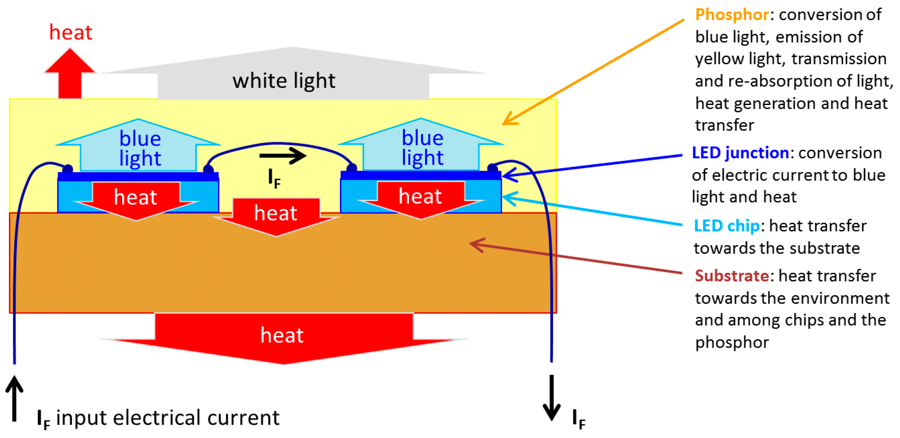
In our current paper, we summarize our multi-domain modeling solution for phosphor- converted LED devices, which is a mixed, compact-detailed model by using one of the “standard” chip-level multi-domain LED models for the description of the operation of the blue pump chips within CoB devices. Only the multi-domain nature of the operation of the blue LED chips can be represented by a compact model; the blue LED chips’ thermal environment (substrate, phosphor) of a CoB device has to be considered by a distributed, detailed 3D model. This way detailed studying of thermal phenomena in the phosphor layer (both in the vertical and lateral direction), including the effect of local interaction of the phosphor and the blue pump LED chips within the CoB array is made possible. In
Figure 1, we provide a summary of physical processes taking place in the different major structural elements of a phosphor-converted white CoB LED device that we aimed to cover with our simulation approach.
The organization of our paper is as follows: In
Section 2, we describe the context and the goals of this work.
Section 3 deals with the major bottleneck: How to identify the material properties of phosphor layers needed for multi-domain simulation. We were inspired by References [
16,
18] to also prepare stand-alone custom phosphor samples that measure the temperature dependency of the phosphor properties. Moreover, with the same phosphor mixtures, we prepared single-chip white LED samples with well-controlled properties in order to allow us to fine-tune and to validate our simulation methods and models. Details on this part of our work are also provided in
Section 3. In
Section 4, we introduce our coupled chip + phosphor multi-domain simulation model along with the description of the light and heat propagation models of different complexity. In
Section 5, we apply the introduced models to a commercially available CoB LED device that has also been characterized by common thermal and optical measurements as well. The comparison of the simulation and measurement results obtained for this device is provided in
Section 6. In
Section 7, we provide a summary and conclusions. In the Abbreviations we provide a summary of abbreviations and symbols used in this paper.
This paper, as a significantly extended version of our THERMINIC 2019 conference paper [
23] provides a comprehensive summary of our CoB LED multi-domain modeling related work (parts of which have already been published at other conferences as well [
24,
25]) completed with a few, recent measurement results.
2. Background, Related Own Work
The work described here has been carried out in the framework of the recently completed European H2020 ECSEL research project Delphi4LED [
26]. The major focus of the project was placed on single-chip LED packages and luminaires made thereof, applying a modular approach in the overall luminaire design process [
27]. In the Delphi4LED approach, multi-domain behavior is treated on LED chip-level, by means of Spice-like compact (lumped) models [
28]. The thermal effect of the LED package physical structure is also described by compact models [
29]. To consider farther elements of the thermal environment, there are two options. On the one hand, the luminaire’s thermal behavior and the effect of its thermal environment can be represented by yet another compact thermal model [
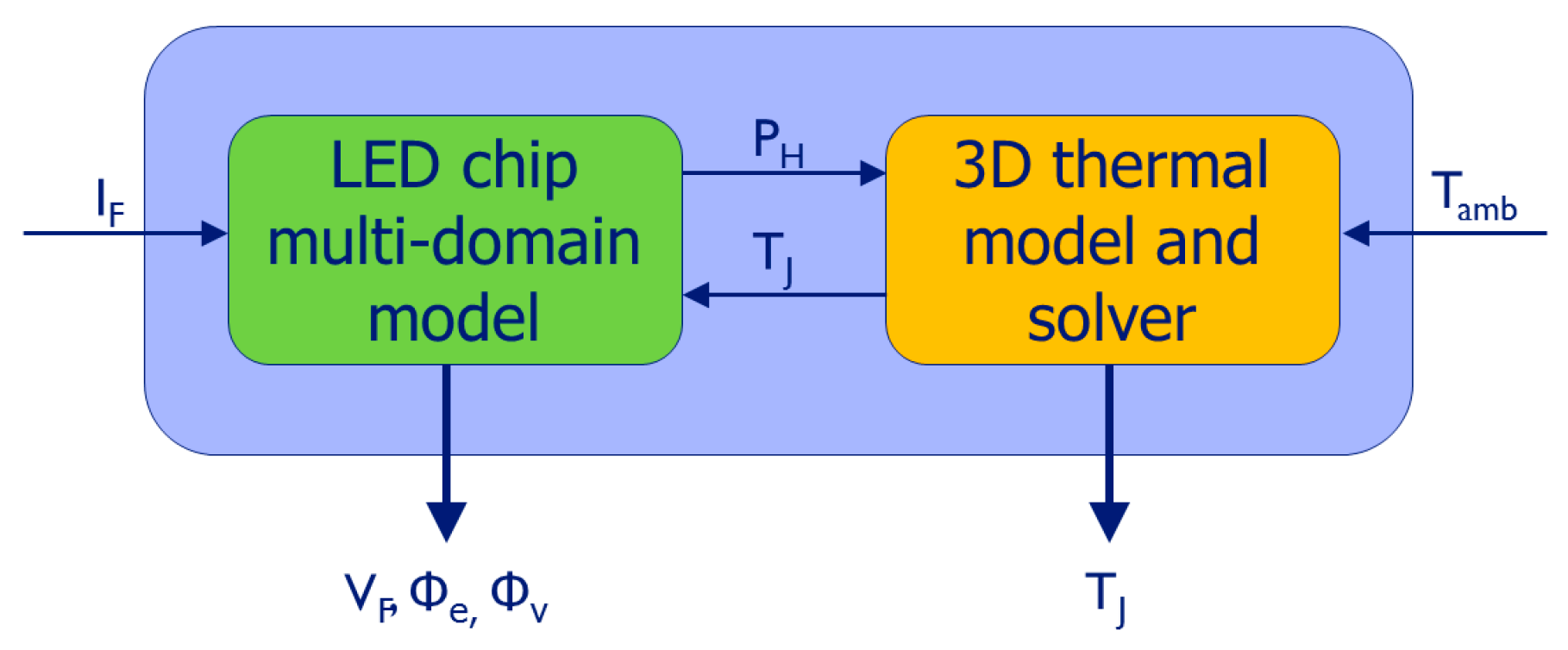
30], and the entire model (including the LED chips models completed with the compact thermal models of their packages) forms a Spice netlist that can be simulated with any Spice compatible circuit simulator. On the other hand, another approach has also been developed within the Delphi4LED project: The 3D thermal environment of the LED chip is considered by a detailed 3D thermal model. In this approach, a 3D thermal simulator is modified in a way that it can iterate between the chip-level multi-domain LED model and the thermal solver, as illustrated in
Figure 2. An implementation of such a scheme was used in the Delphi4LED project to demonstrate the use and benefits of the “industry 4.0” like design workflow suggested by the project [
31].
In the case of phosphor-converted white CoB LEDs, however, the first approach of using compact models only cannot be applied because of the distributed, multi-domain nature of the phosphor layer, involving:
Considering the light propagation properties in 3D (absorption/transmission);
Temperature dependence of phosphor properties (among those, that of the conversion efficiency);
The resulting heat generation and temperature rise in the phosphor layer.
This is illustrated in
Figure 1. The thermal effect of the phosphor layer (distributed heat source over the entire area of the CoB device) cannot be separated from the thermal behavior of the rest of the structural elements of a CoB LED, therefore:
Regarding the description of the multi-domain behavior of the blue LED chips, we relied on one of the Spice-like multi-domain LED models we developed earlier [
28]. The heat transfer within the bulk of the LED chips, the ceramics substrate and within the phosphor layer is treated by BME’s proprietary conduction-mode only thermal field solver [
32,
33] that has already been successfully adapted to the multi-domain modeling of large-area OLED devices [
34,
35].
The most important differences and similarities between the former multi-domain OLED simulator and the present approach for CoB LEDs are the following:
The multi-domain behavior of OLED junctions is of distributed nature while in CoB LED devices, the junctions of the individual blue LED chips are represented by a compact (Spice-like) multi-domain model.
Thermal modeling of the light-emitting polymer layer (LEP) of OLED and the phosphor layer of CoB LEDs is similar: In both cases heat, transfer in these layers need to be modeled along with the heat generated by conversion losses. The way how the dissipated heat in these layers is calculated, however, is different. In the OLED model, the LEP layer was considered two-dimensional; the heat was generated at the point of the light emission. However, the phosphor layer of CoB LEDs requires complex handling of a true three-dimensional model of light and conversion losses. For modeling the heat transfer, the layer thickness and thermal conductivity have to be known.
Both in OLED LEP layers and in CoB phosphor layers conversion efficiency (electricity to light in the case of OLED LEPs, blue light to yellow light in CoB LED phosphors) depends on the local temperature.
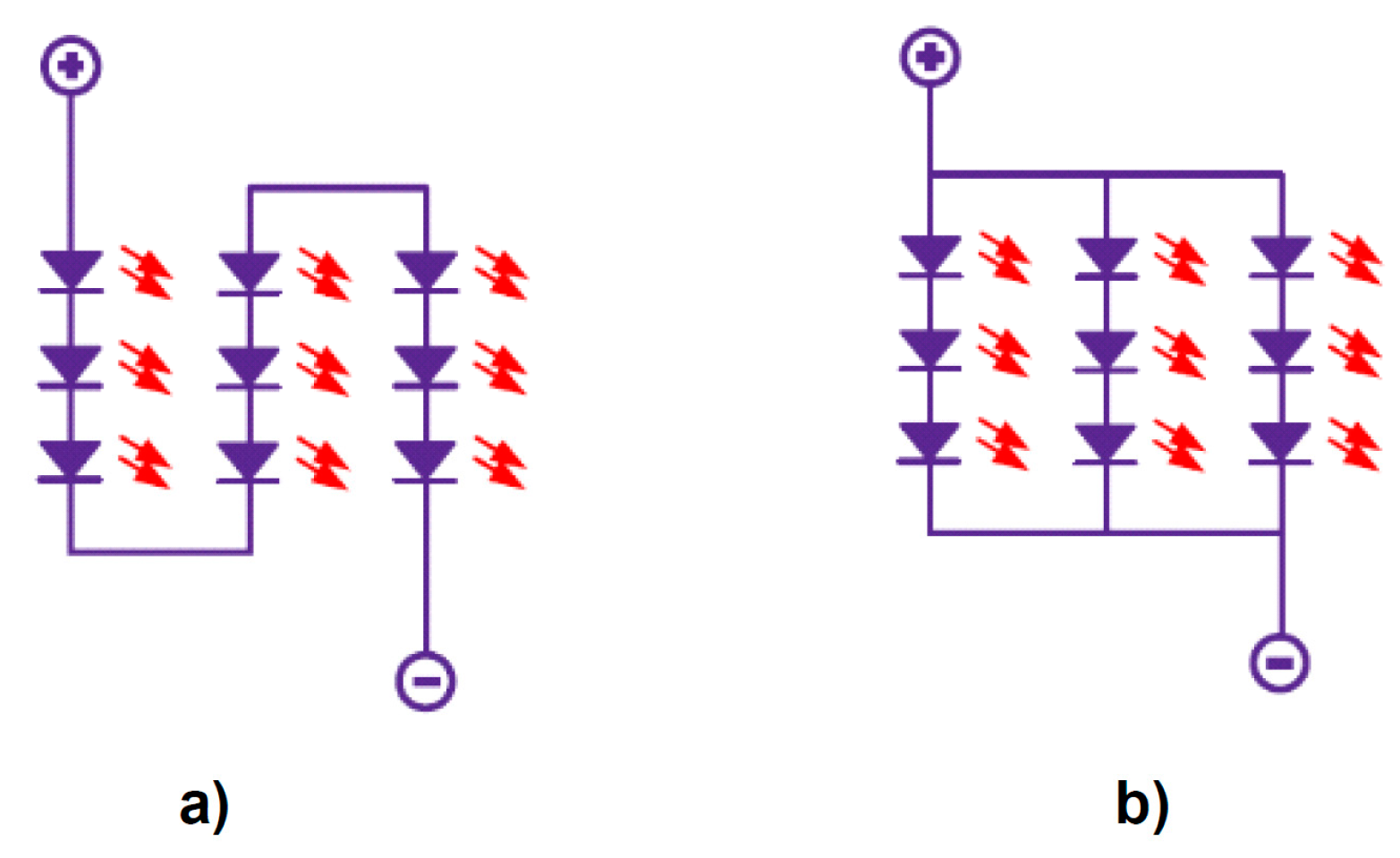
The electrical interconnect network of blue LED chips of a CoB device is considered as zero-dimensional electrical nodes (with no voltage drop in the interconnects). The typical electrical configurations of LED chips inside a CoB device are shown in
Figure 4.
As seen in
Figure 4, none of the electrical configurations of the arrays of blue LED chip inside a CoB device provides individual access to any of the chips within the array. This means that with the common
forward current we power the entire LED array and we can measure the total radiant/luminous flux of the entire array that is the sum of the fluxes emitted by the individual chips and converted by the phosphor. For a single LED string, the situation is the same for the overall forward voltage of the string. These measured characteristics are called ‘ensemble’ characteristics in the JEDEC JESD 51-51 standard [
36].
The relationship between the overall, ensemble characteristics of an LED array and the individual chip characteristics (as illustrated in
Figure 5 for the forward voltage) are
where
represents either the radiant flux,
or the luminous flux,
,
is the number of the LED chips in the LED string forming the LED array.
and
represent the average forward voltage and flux data that can be related to an individual LED chip within the array.
This means, that the measured isothermal IVL characteristics of a CoB device need to be post-processed before applying the parameter extraction procedure to obtain the multi-domain chip-level model parameters to be used by the chosen Spice-like multi-domain LED model. Note, that in the case of using a combined thermal and radiometric/photometric test setup as suggested by the JEDEC JESD 51-51 and JESD 51-52 standards [
36,
37] for CoB LED measurements, there is no way to identify the
individual junction temperatures of the blue LED chips within the entire array. As the best approximation, one has to calculate with the
temperature as if it was a uniform temperature for each LED chip within the CoB device. Thus, the set of isothermal IVL characteristics is given by the
and
data as given by Equation (2) and Equation (4), respectively.
To test the validity of the Equations (1)–(4) we created an array from individual LED packages on a cold plate with a diameter of 12 cm that was attached to a 50 cm integrating sphere. In this setup, the LEDs could be powered and characterized both individually and together as an array of LEDs. It was found that the chip-level characteristics derived from the measurement results of the entire array were very close to the averages of the individually measured voltages and fluxes, suggesting that the above-mentioned approximation for the individual characteristics of the individual LED chips is acceptable.
4. Multi-Domain Modeling: Chip-Phosphor Interaction, Light and Heat Propagation
From now on, we call the color of the absorbed light of the primary emitter LED chips as blue and the converted and re-emitted light color as yellow. For modeling phosphor layers different effects need to be considered, such as blue absorption, blue scattering, blue-to-yellow conversion (Stokes shift), yellow absorption, yellow scattering and the temperature dependence thereof, if applicable.
We distinguish our phosphor models according to the way the light path is followed in 1D (distance from the source), or in 3D. In certain cases, the absorption and reflection on the LED chip/substrate surface are taken into account. In the following section, we discuss these approaches with their possible limitations.
4.1. A 1D Phosphor Model
In our 1D model, we consider the blue and yellow absorption and the wavelength conversion. We use simple formulae to approximate the optical (radiant) power of the blue and yellow light, and for the heat generated due to conversion and absorption losses.
When the blue light propagates through the phosphor layer, it may be absorbed or converted by the phosphor particles. Assuming that the particle concentration in the phosphor layer is homogeneous, the blue photon number follows the Lambert-Beer law:
where
is the blue photon number at distance
(measured from the source),
is the originally emitted photon number (calculated from the optical power),
μb is the sum of the attenuation and conversion coefficients
, and is proportional to the probability of hitting a phosphor particle. As there is no yellow light emitted from the LED chips, the source of yellow photons is the conversion by a phosphor particle, so the number of yellow photons can be written as:
where
is the conversion coefficient.
Considering the yellow attenuation from the distribution of yellow source:
Note that the converted yellow photons do not follow the direction of blue photons. The direction of propagation of the converted yellow photons can be assumed to be isotropic. Therefore, only half of the converted yellow photons will propagate away from the LED.
The other half starts to move in the direction of the surface of the LED chip. Let the thickness of the phosphor layer be
and let the yellow source
be above point
of the blue source, where the photon number sought can be described as:
The attenuation of that source from
also given by the Lambert-Beer law:
With the help of integration, we can get the formula for the photons arriving above point
:
The number of yellow photons reflected from the LED chip surface is calculated from the power of yellow light incident at the surface. The latter is
Considering also the
reflection coefficient (the ratio of reflected and absorbed photons), and the attenuation from the LEDs surface we get:
Considering that in each direction half of the number of photons is emitted, the final formula for the yellow photon number is:
From the known wavelengths of the photons, the energies of the blue and yellow photons and the energy difference, due to wavelength conversion can be calculated as follows:
With the above energy values, the dissipation density at point
can be expressed with the original blue photon number,
as follows:
With this analytical formula, we can determine the parameters of the phosphor layer by measurement, although,
We neglected that the light emitted from the chip has an angle distribution;
There is no scattering considered in the model;
Furthermore, in Equation (14), we assumed a single blue and yellow wavelength and did not deal with the actual spectral power distributions of the original blue and the converted longer wavelength light.
The neglected effects do not result in a significant error in the thermal model, if the phosphor layer is much thinner than the dimension of the light emitting surface of the blue LED chips.
4.2. Simplified 3D Phosphor Model
The simplified 3D model is an extension of the 1D model to 3D. The scattering is still neglected, but the spatial light distribution is taken into consideration now. To keep this model simple, we do not calculate with the attenuation of the yellow light. The main question to answer with the use of this model is how the overall heat generation distribution will be affected by the losses in the phosphor.
In this approximation the Lambert-Beer law is used again, which gives us the relation between a point on the surface of the LED chip (
) and one in the phosphor layer (
):
where
is the number of nodal (
) emitted photons. Since every location of the lighting surface is considered as a point-like source we have to correct the formula as follows:
To get the number of blue photons at location
, an integration over the lighting surface is needed:
Considering now the
spatial distribution of the blue light we get
The computation for this surface integral for a 100 by 100 mesh lasts a few minutes for each plane that is modeled in the phosphor layer. In order to calculate with the yellow light propagation, we can use the calculated blue photon number, as it is proportional to the source of yellow light:
which increases the computation time to hours for every point. The reflection can be handled by a mirrored blue light source (situated on the backside). This computational cost implies that the analytical formulas should not be used even with a simplified 3D model. The practical workaround to this computational cost issue is to use numerical methods, such as the Finite Volumes Method (FVM).
4.3. Detailed 3D Phosphor Model with a Numerical Approach
The approach of overall modeling of a CoB device described in the present study was inspired by our previous work that targeted multi-domain simulation of large-area OLEDs [
34,
35]. For OLED simulations the FVM was applied to get a 3D network of multi-domain elementary cells. This network was solved by the Successive Network Reduction (SUNRED) method [
32,
33] and the solution provided voltage, temperature, radiance and luminance maps as a response to a given, assumed driving current of the investigated device.
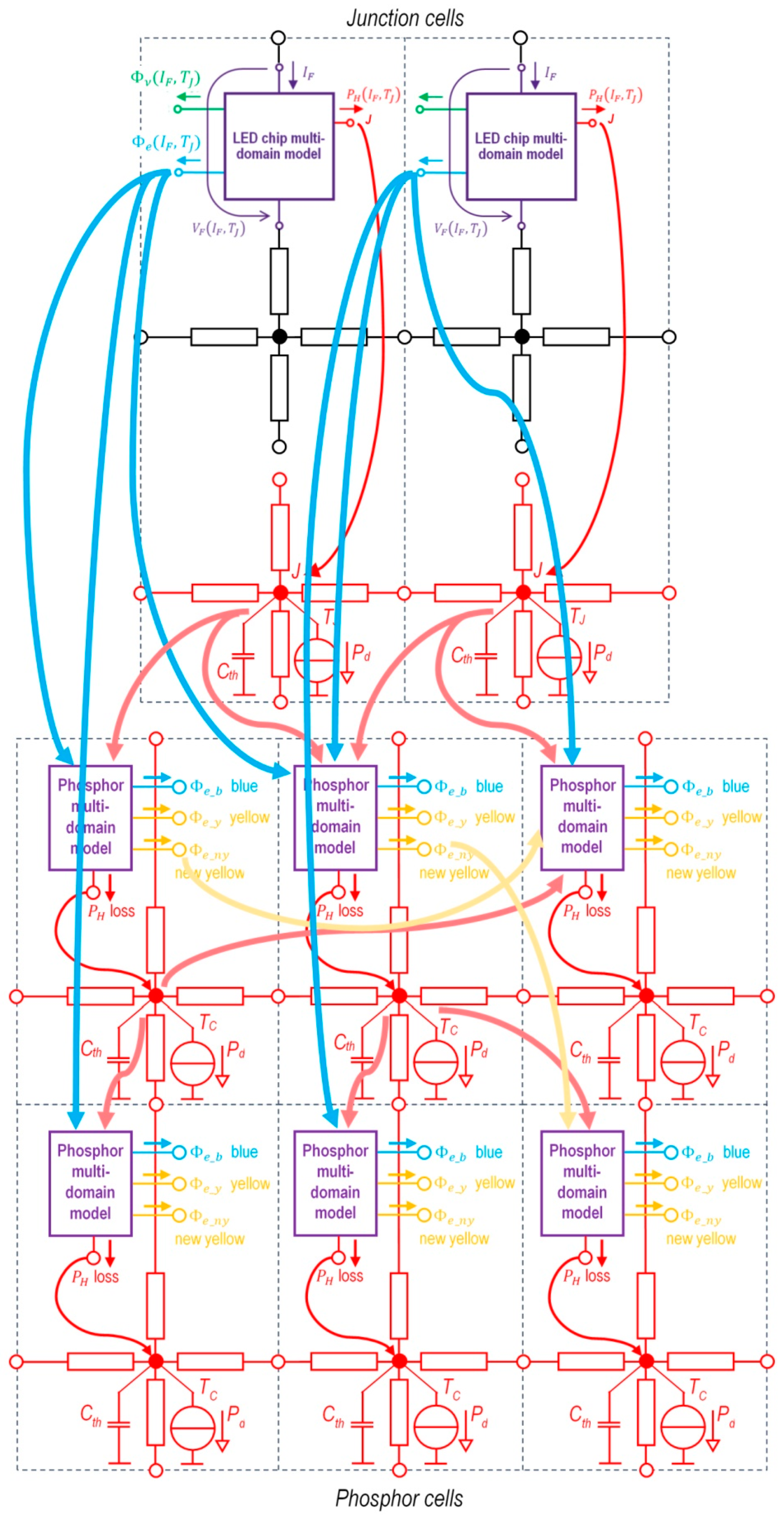
For the simulation of phosphor covered (inorganic) LEDs, we created two special elementary cell models: One for the pn-junction of the LED (describing the multi-domain behavior of the blue LED chips by a Spice-like model) and another multi-domain simulation grid cell type for the phosphor, as illustrated in
Figure 13 (for the sake of simplicity for a 2D case). These models will be detailed in the next subsections.
4.3.1. Junction and Phosphor Cells
A ‘junction cell’ is basically a special cell that represents the bulk material of the LED chip from thermal perspective, but it also incorporates the new, constant forward current-driven formulation of the Shockley-model based multi-domain LED model that we developed previously within the Delphi4LED project [
28]. For every single blue LED chip in the CoB device a local instance of this model is applied, considering the local junction temperature (
) in the FVM simulation grid cell where this model is attached to, see
Figure 13. Such a grid cell is called a ‘junction cell’.
This LED chip model is connected to the electrical model of the cell at its interface to other regions of the device, see the black network elements in
Figure 13. The two input quantities of the junction model are the constant forward current flowing through it (
) and the temperature of the junction (
. ).
Its four output quantities are the forward voltage (), the generated heat flux (), the emitted radiant flux () and the emitted luminous flux ().
The
power provided by the LED chip multi-domain model instances is the local heat-source of the FVM grid cell, represented by the
generators in the generic thermal grid cell. The calculated
radiant flux of a junction cell is split among the blue light rays that are propagated towards the ‘phosphor type’ simulation grid cells of the FVM solver (see the light blue arrows in
Figure 13).
The ‘phosphor cells’ include the same thermal part as an ordinary structural material or the ‘junction cells’ (red thermal network elements), and they also include a phosphor multi-domain model, describing the light conversion and propagation and the corresponding thermal losses in the phosphor material.
The calculated thermal loss is the local
heat-source of the given FVM grid cell. Note, that in
Figure 13, symbol
is used both for the multi-domain model of the LED chips and for phosphor regions to denote the local heating power.
4.3.2. Modeling the Light Conversion in the Phosphor
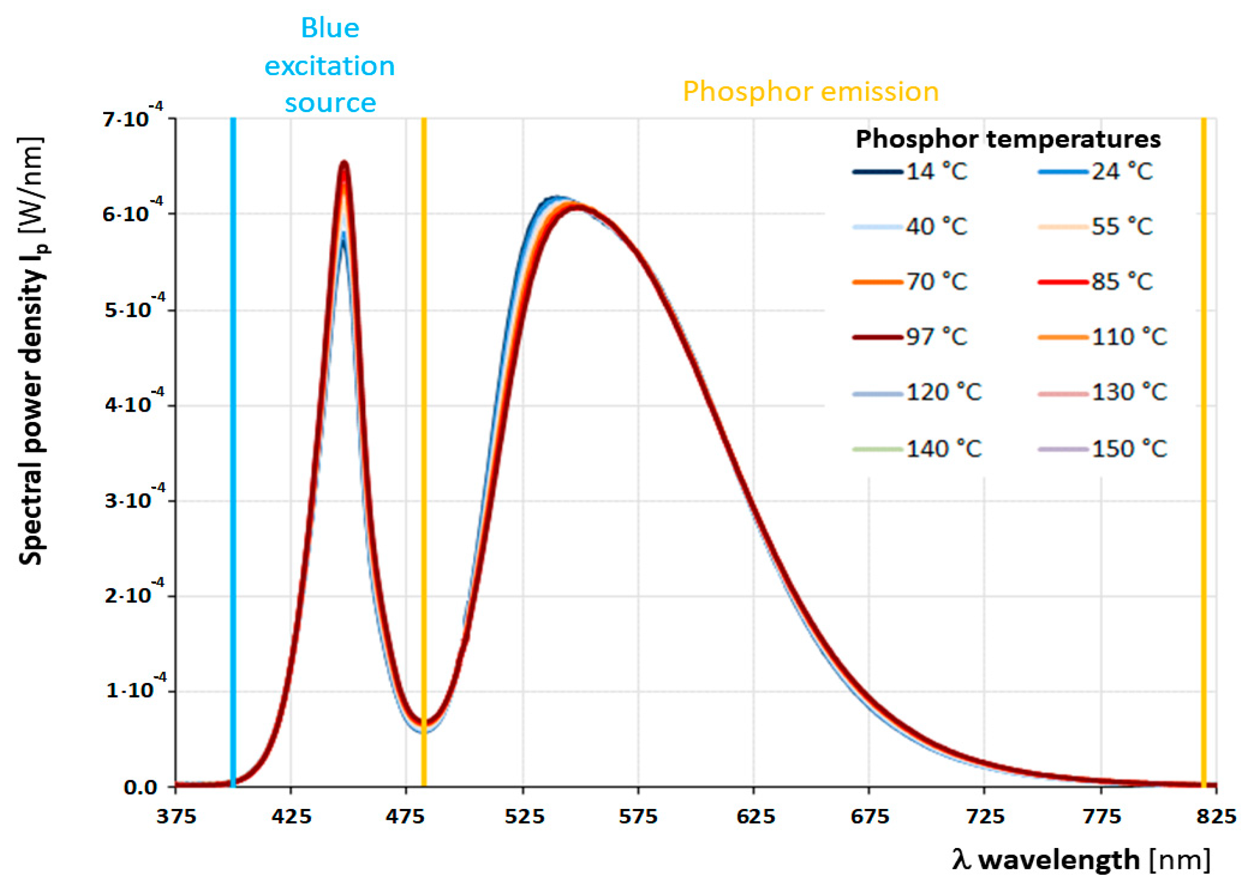
The chip-level multi-domain LED model that we use calculates the total emitted radiant/luminous flux only; it does not provide actual spectral power distribution of the emitted light Therefore, we considered only the blue and converted yellow fluxes, without any details about their actual spectral power distributions. Note, however, that the following discussion is also valid for all colors in the entire spectral range of the emitted converted light, ranging up to red as well and with an additional model for the absorption and emission spectra of phosphors, temperature-induced slight spectral changes like the ones seen in
Figure 8 could also be included.
The wavelength conversion results in a loss of energy, which heats up the phosphor. Because the phosphor particles are mixed with transparent but poorly heat-conductive material (e.g., silicone) as a host matrix, their temperature can be significantly, even tens of degrees higher than in other parts of the LED package. The conversion is temperature-dependent, therefore, a multi- domain simulation of the phosphor is required.
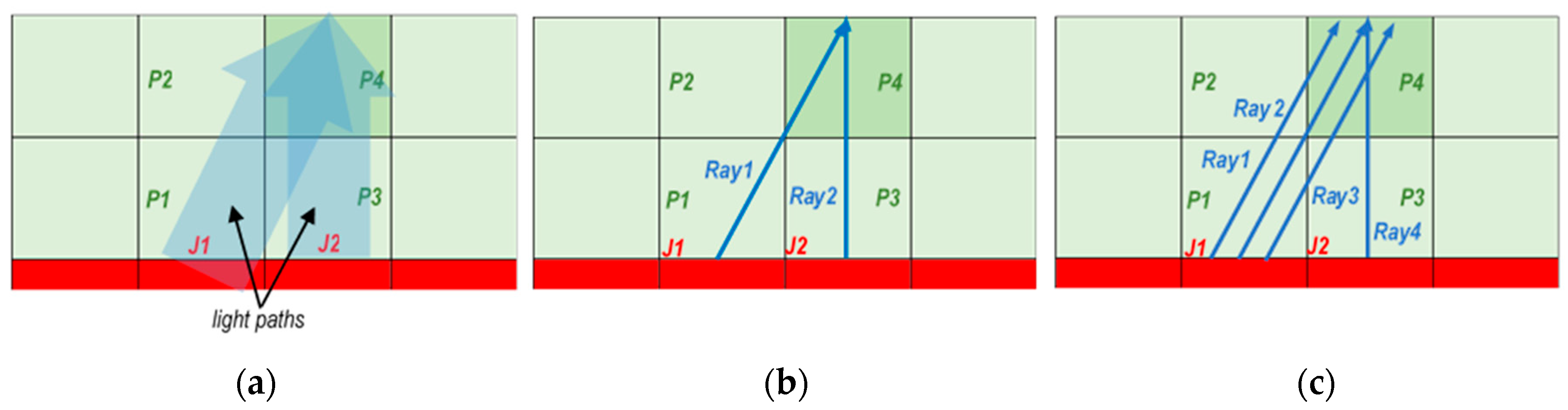
Figure 14 shows some light paths in an LED package. Blue light is emitted in different directions from the LED chip, which may reflect from the surfaces, even crossing the phosphor layer several times. Meanwhile, the blue light is partially converted to yellow. The emitted yellow follows different paths than the blue light absorbed by a phosphor particle; it may propagate in any direction. The yellow light can be reflected several times, and it can be absorbed and re-emitted in different directions. The energy loss due to the absorption of yellow light also contributes to the temperature rise of the phosphor layer.
We assume again, that the attenuation of the blue and yellow fluxes follows the Lambert-Beer law:
where
and
are the blue and yellow attenuation coefficients,
is the effective thickness of the phosphor layer. Equation (22) refers to the case where the yellow light is not produced in the layer but enters from the outside (transmitted yellow). The absorbed blue and yellow fluxes can be calculated as
The yellow flux converted from the absorbed blue flux can be calculated as
where
is the conversion efficiency. A part of the absorbed yellow may be re-emitted:
where
is the “yellow-to-yellow conversion efficiency”, characterizing the re-emission. The yellow output of a phosphor layer is the sum of the transmitted, converted and re-emitted yellow:
The heating power due to the conversion loss is the difference between the absorbed blue and the converted yellow radiant fluxes:
The heating power due to the yellow transmission loss is the difference between the input and the transmitted and re-emitted yellow fluxes:
The full heating power of the phosphor layer is the sum of the absorption and transmission losses:
4.3.3. Rays split over the FVM Simulation Grid Cells
The FVM simulation calculates the quantities per elementary cell—therefore, the absorption and transmission losses, as well as the blue and yellow output fluxes, are determined for the elementary cells of the phosphor layer. The idea behind the method comes from the ray tracing [
46] and path tracing [
47] algorithms used in global illumination.
The goal is to create a generic cell model that can handle all-optical and thermal phenomena presented in
Section 4.3.2 (as illustrated in
Figure 13), and leaves the definition of the light paths to the user. The quantities are determined for each elementary cell individually.
In a cell-split model, light propagates in a beam from the internal volume or from a surface of a cell to the outer surface of another cell. For example, blue light typically propagates from the surface of junction cells to the outer surfaces of a phosphor layer, as illustrated in
Figure 15a Handling 3D beams would require integral calculation. To avoid this complicated and time-consuming method, we use 1D rays as in ray tracing methods, see
Figure 15b. A ray is defined by the coordinates of its start and end points. In this model, based on Equation (21), the blue output flux for Ray 1 is:
where
,
and
are the attenuation coefficient, temperature and distance traveled by the light in cell
n, respectively.
is the flux of the junction cell in the direction of the output surface. As
is the distance between the entry and exit points of the ray in the cell, and the temperature and the material are considered homogeneous in a cell, this is a simple calculation. The other equations presented in
Section 4.3.2 are similarly simple to re-write for this discretized view.
If the 3D beam is replaced with a 1D ray, an error is introduced in the calculation that can be reduced by considering multiple rays from the starting surface to the target surface, as illustrated in
Figure 15c. (This method is well known in computer graphics for antialiasing purposes).
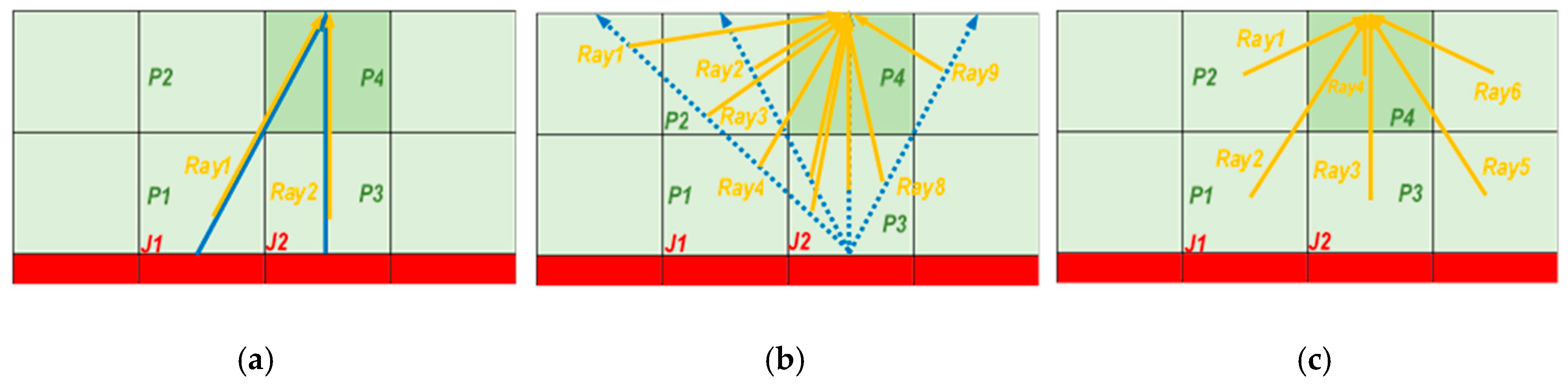
Different strategies are possible to handle yellow rays. If the 1D light propagation, shown in
Section 4.1 is used, the blue ray and the converted yellow will further propagate together. The method is also applicable for 3D blue propagation (
Figure 16a), although the result will obviously be inaccurate. A more accurate result can be obtained by determining the flux of the yellow light emitted from a blue ray in a cell and how much of it is radiated towards an outer surface. This will be a yellow ray (
Figure 16b). The re-emitted yellow rays can come from the yellow rays in a similar way.
How many rays will be in total if the phosphor region is a rectangular cuboid of cells with one surface in contact with the blue chip’s junction cell? The number of junction surfaces, in this case, is . If 1D light propagation is used, a single ray will leave every elementary junction surface, resulting in a total of rays. Using our 3D light propagation model, blue rays start from every junction, one for each outer surface. The number of outer surfaces of the phosphor is , so the number of blue rays . Each blue ray triggers a yellow ray from each intersected cell to each outer surface. If the number of intersected cells is estimated to be , then for the number of yellow rays we obtain . If, for example, , , then , , , , .
The number of yellow rays is by several orders of magnitude greater than the number of blue rays, and the re-emitted yellow rays have not yet been addressed. A realistic model of a real LED device requires a higher spatial resolution of the FVM grid—thus, the number of yellow rays would increase to such a high value that one cannot manage. Therefore, we need a modeling approach where the number of yellow rays to follow is significantly reduced: This is the “indirect yellow ray model” illustrated in
Figure 16c. In this model, for each cell, the amount of yellow flux generated by the blue rays passing through and the re-emitted flux generated by the passing yellow rays are cumulated. In a subsequent iteration step, this cumulated flux is considered as the total yellow flux emitted by the cell, and one yellow ray per cell will be started for every outer surface. (Since this uses the flux calculated in the previous iteration, it is not derived from the flux generated by the junction cell in the current iteration, so the calculation is indirect). The number of yellow rays, thus, depends on the number of phosphor cells and the number of the outer surfaces. Using numbers of the previous example the number of the yellow rays is
—by three orders of magnitude less, therefore, manageable.
4.3.4. Phosphor Cell Model
The phosphor multi-domain model is built in the thermal FVM model of the phosphor cells, as shown in
Figure 13. The model delivers four output quantities:
Local heating power, : The power to heat the simulation grid cell resulting from conversion losses. This is the value of the heat-flux forced by generator into the thermal network model associated with every finite material volume represented by a simulation grid cell;
The new yellow radiant flux, , the sum of the yellow radiation produced by conversion from blue light passing through the cell and the re-emitted radiation from the yellow light passing through the cell;
The blue radiant flux leaving the cell, , the remainder of the input blue flux after conversion;
The yellow radiant flux leaving the cell, , the sum of the input yellow radiant flux remaining after the attenuation in the cell and the calculated new yellow flux, .
Two of these quantities, and directly influence the operation of the actual simulation grid cell where they were calculated, the other two values (, ) are stored as simulation results.
The model calculates the total output quantities for rays starting from the junction cells, taking into account the temperature and material parameters of each cell crossed by them.
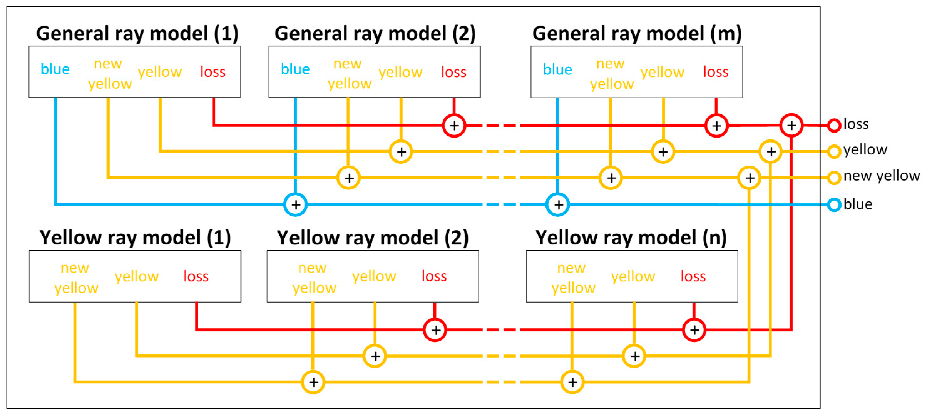
The structure of the phosphor cell model is shown in
Figure 17. The output quantities are calculated individually per ray, and then they are summed. There are two types of ray models.
The general model describes one ray that travels from a junction cell to a particular phosphor cell. It can be a blue, a yellow or a mixed ray (such as in
Figure 16a). Blue rays were shown in
Figure 15b, yellow rays are shown in
Figure 18: the ray starts as blue at the junction, then it is converted in a cell and continues its path to a given destination as a yellow ray.
The yellow ray model describes a ray starting from a phosphor cell containing only yellow component, see
Figure 16c. The yellow ray model uses less memory than the general ray model. The general model must be used at junction cells, and the yellow model can be used at phosphor cells.
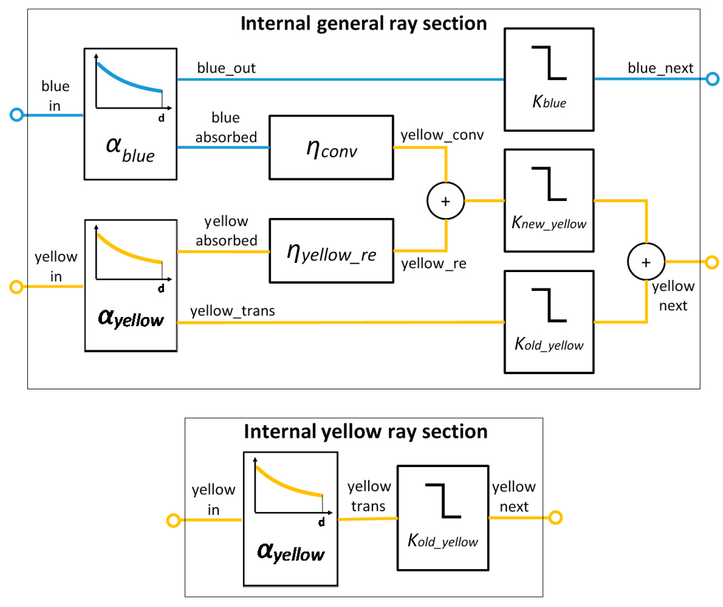
The ray models represent a ray by sections corresponding to individual cells it crosses, see
Figure 19. Generally, multiple rays leave the starting cell, the amount of flux in a given ray is controlled by the proper adjustment of the
multiplier factor. The internal ray sections calculate the input blue and/or yellow flux of the current cell, the ray model of the cell cascade in the path calculates the output quantities of the current cell.
Each internal ray section corresponds to a cell in the space between the starting cell and the current cell, using the temperature and material parameters of that cell. The structure of the general and yellow ray sections is shown in
Figure 20.
If a ray suffers an imperfect reflection at the i-th section of its path, we can model it by adjusting the -values of section i. In the case of reflection, sections i and i + 1 usually belong to the same phosphor cell.
The fluxes of the input rays are transferred to the and blocks of the model. These blocks represent attenuation according to Equations (21) and (22), as well as absorbed fluxes according to Equations (23) and (24). The and attenuation factors are temperature-dependent material parameters of the cell. The and blocks represent the blue-to-yellow and yellow-to-yellow conversion efficiencies, which are temperature-dependent material parameters, as seen in Equations (25) and (26).
The K blocks control the amount of the resulting flux propagated to the next ray section. These blocks correspond to a constant multiplication, most often zero or one.
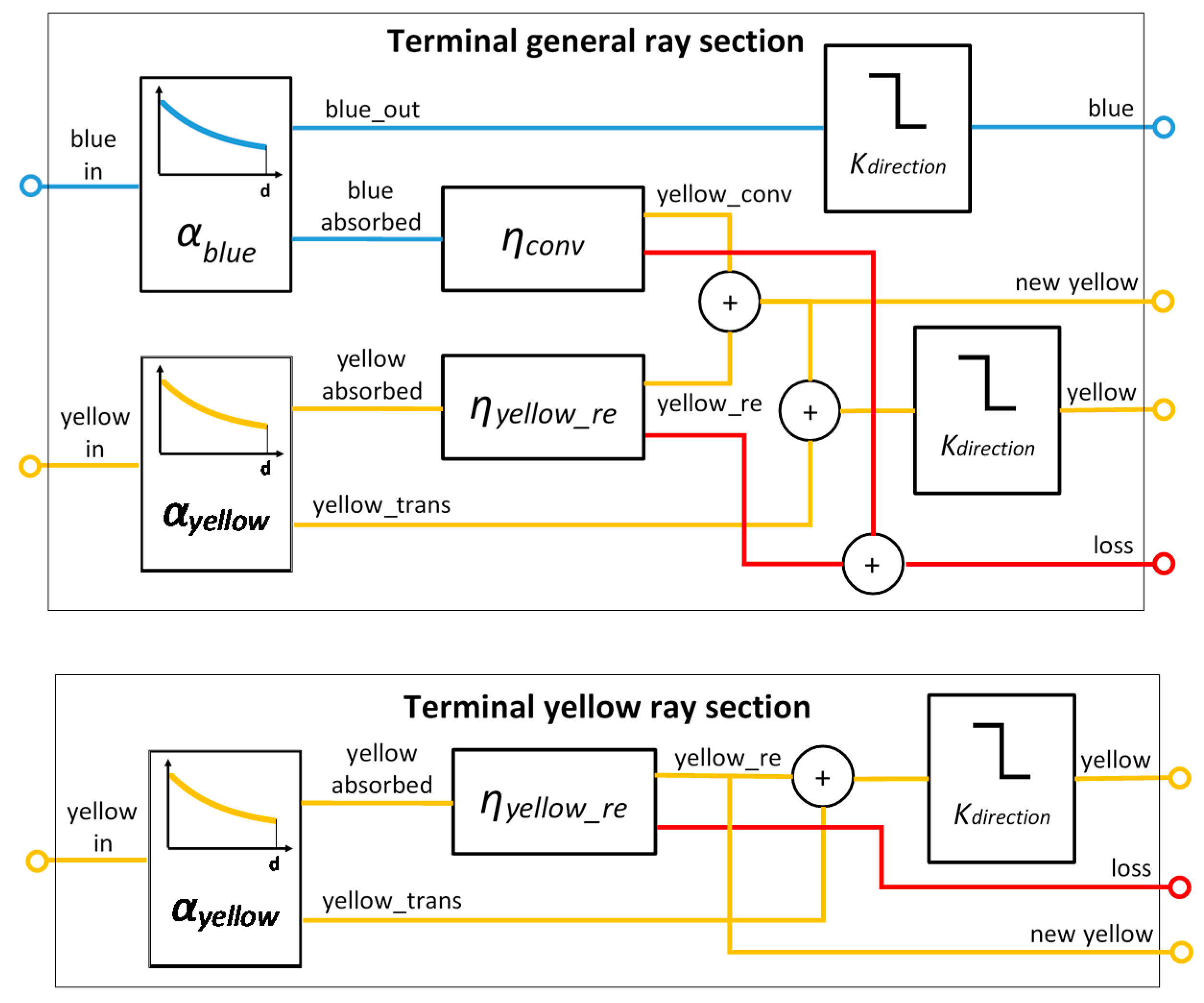
The structures of the general and yellow ray sections are shown in
Figure 21. The terminal sections differ from internal ones in that they calculate both new yellow flux and
power loss of the conversion as described by Equations (28) and (29).
4.4. The Use of the Simple 1D and of the Complex 3D Models, Extraction of Phosphor Model Parameters
The 1D model provides fairly good accuracy for thin phosphor layers (much thinner than the lateral dimensions of the layer). Therefore, with an appropriate set of phosphor samples, it can be used for the extraction of phosphor material properties (model parameters), such as absorption rate or conversion efficiency. With the set of model parameters identified, the 3D phosphor model is used for accurate simulations.
As described in
Section 3.3, phosphor-converted white LEDs have been created using fully pre-characterized bare blue ones, with five different phosphor layer thicknesses, realizing five different spectral power distributions, thus, realizing light output with different CCTs. (The mass fraction of the phosphor powder has also been varied; see the applied mass fractions in
Table 1).
On the one hand, these LEDs with known properties have been used for extracting material properties for the multi-domain model as mentioned above [
25], and on the other hand, for validating the overall simulation approach (with the blue chip multi-domain compact model embedded), simulating them characterized single-chip white LEDs well. The major steps of extracting the phosphor layer parameters were the following:
- (a)
Spectral power distributions for all manufactured custom-made white LEDs have been measured (along with the spectra of the used bare blue LEDs before attaching the phosphor + lens structure).
- (b)
We separated the spectra into ‘blue’ and ‘yellow’ parts (as illustrated in
Figure 8 for large, stand-alone phosphor samples), in order to allow us to determine the number of ‘blue’ and ‘yellow’ photons. (For the calculation of the number of yellow photons a rough spectral power distribution was assumed).
- (c)
From the blue photon number distribution, the sum of the attenuation coefficient for blue light and the conversion coefficient can be determined.
- (d)
From the yellow photon number distribution (four points), the remaining coefficients (blue attenuation, yellow attenuation and reflection) can be determined.
Note, that the spectral power distribution of the ‘yellow’ light can be better approximated by assuming multiple wavelength bands of the ‘yellow’ light (in an extreme case bands correspond to the wavelength resolution to the measured spectra). This would assume, however, as many yellow ray models as many yellow wavelength bands are assumed. (The execution time of the ray model would linearly scale with the number of the assumed yellow wavelength bands).
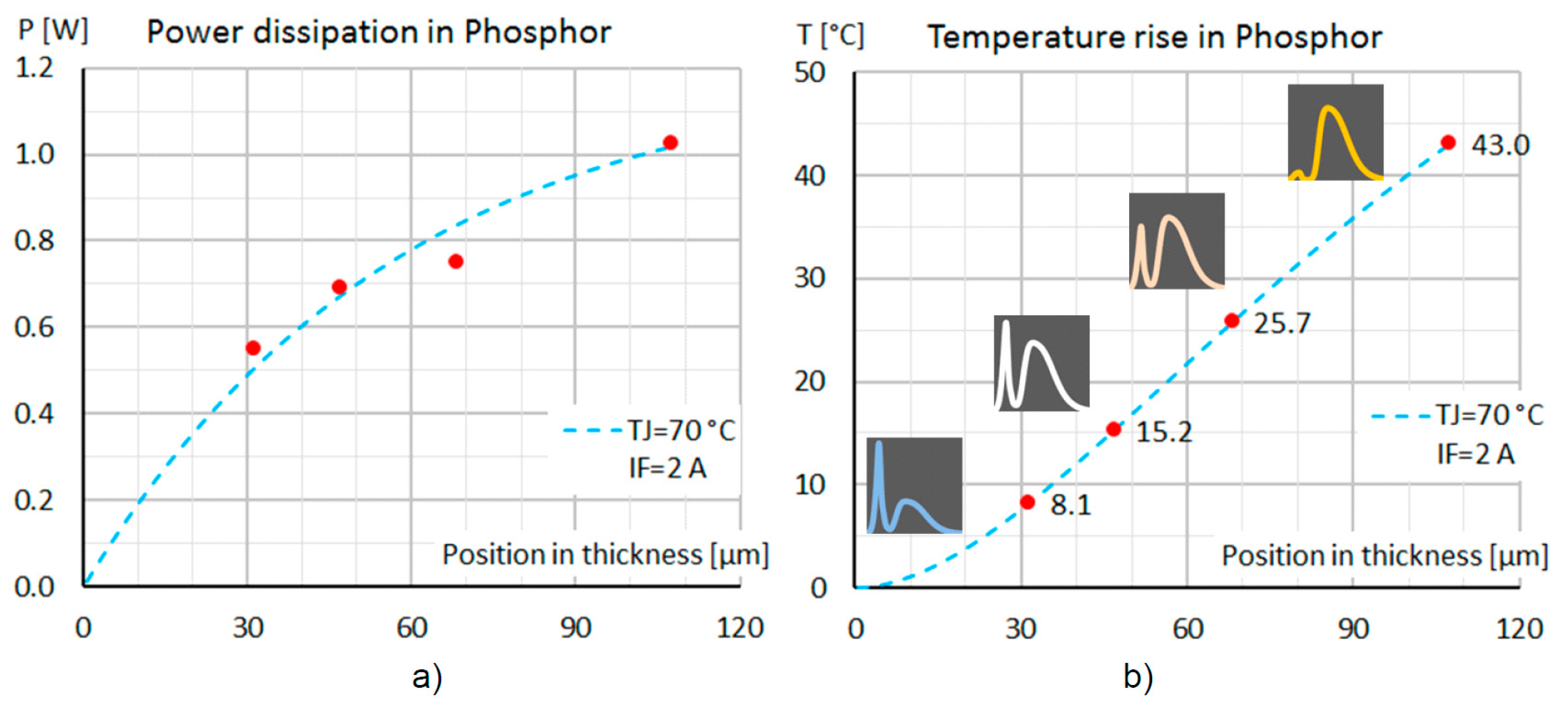
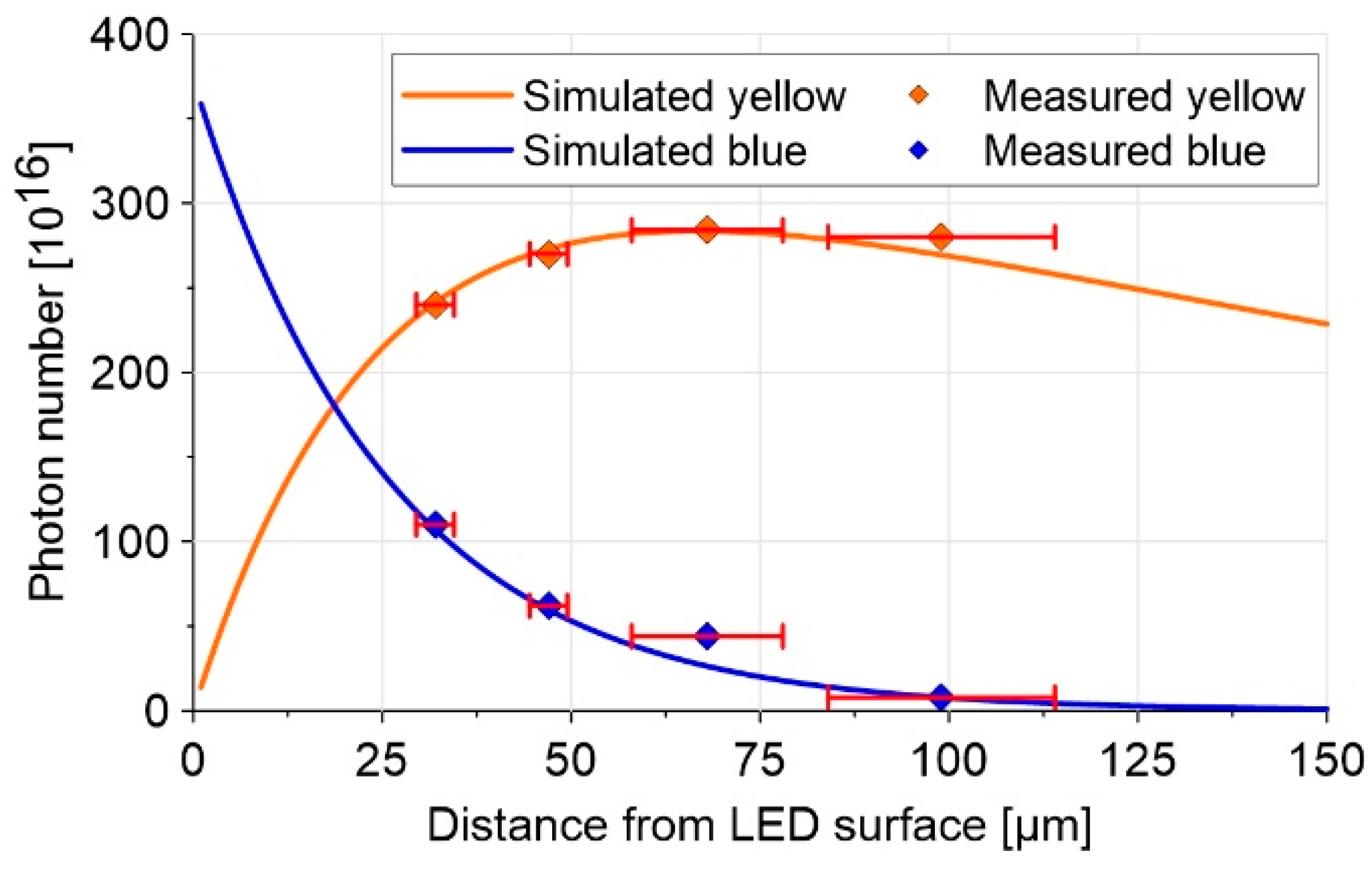
We measured the SPDs of all custom-made white LEDs. The spectrum measurement was done on five samples with different phosphor layer thicknesses (0 µm (blue LED), 32 µm (cool white LED), 47 µm (neutral white LED), 68 µm (warm white LED), and 99 µm (amber LED)), at five different blue LED junction temperatures (30 °C, 50 °C, 70 °C, 90 °C and 110 °C) and each with six different forward currents (100 mA, 350 mA, 700 mA, 1000 mA 1500 mA, 2000 mA). From the total of 150 spectrum measurements, we present data for five measurements only, for demonstration purposes (the applied measurement conditions were: Fifty degree Celsius ambient temperature and 1000 mA forward current). The calculated photon numbers are summarized in
Table 2.
For the blue photon numbers, we can fit an exponential, with a coefficient of m, from the yellow data, we can determine the missing coefficients. As Equation (12) is transcendent there are more solutions, but physically only one is found to be correct: (, where the length is given in µm, so the dimension of the coefficients is m.
The measured blue and yellow photon number versus the 1D prediction is shown in
Figure 22. As the diameter of the LED chip is 1.6 mm, theoretically, the accuracy range of the 1D model is 0–160 µm in phosphor layer thickness. Comparing the measurement data to simulation results suggests that the method provides sufficient accuracy. The measurements at other LED operating points (junction temperature, forward current) show less difference in the extracted parameters than the inaccuracy of the calculated parameters. For different concentrations of phosphor powder the coefficients can be scaled, as the original relationship between the coefficients and the physical effect was the Lambert-Beet law, where the attenuation coefficient is proportional to the attenuation cross-section, which is proportional to the phosphor powder concentration:
. The phosphor temperature rise inside the phosphor layer with respect to the junction temperature can be determined through the integration of the heat distribution.
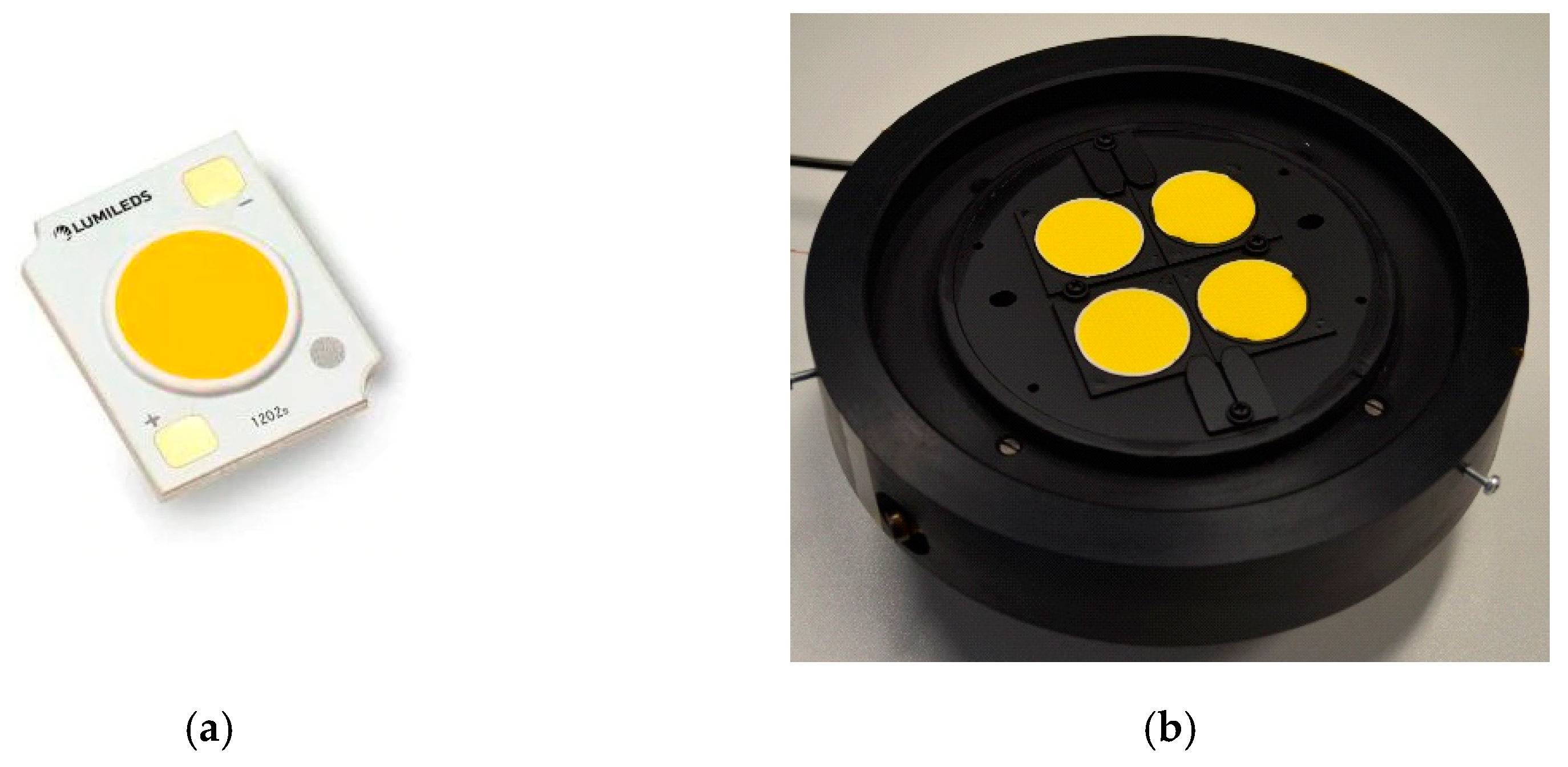
5. Simulation of a Commercially Available CoB Device
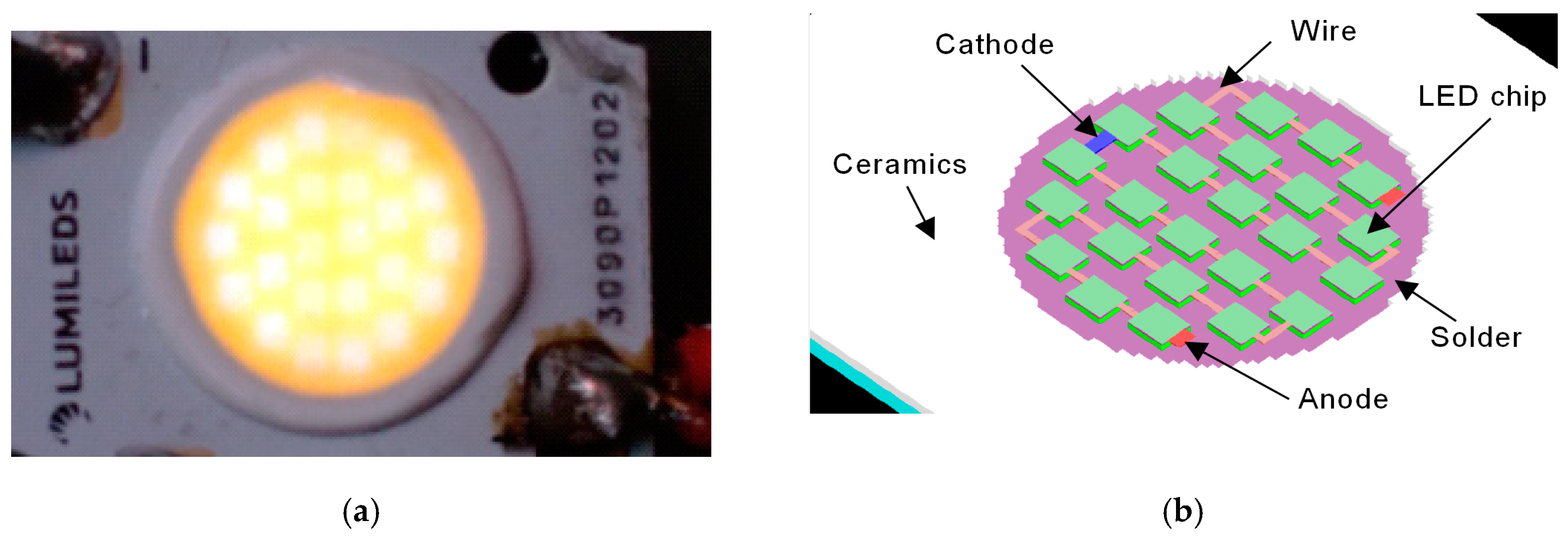
We measured and modeled a Lumileds 1202s CoB LED device which consists of 24 LED chips (two strings of 12 LEDs, connected in parallel) with a lateral dimension of 600 µm × 700 µm each, placed on an aluminium pad with solder layer between them, covered by a phosphor layer, see
Figure 23a. The parameters of its phosphor coating were measured as outlined in
Section 3.2, see further details in Reference [
25]. A 3D model was created for simulation (
Figure 23b). In the numerical simulation model the 650 µm thick phosphor was divided into nine layers of equal thickness. The parameters of the multi-domain LED chip model were extracted from the measured ‘ensemble’ characteristics. The coefficients of the phosphor model were extracted from the measured spectral power distributions.
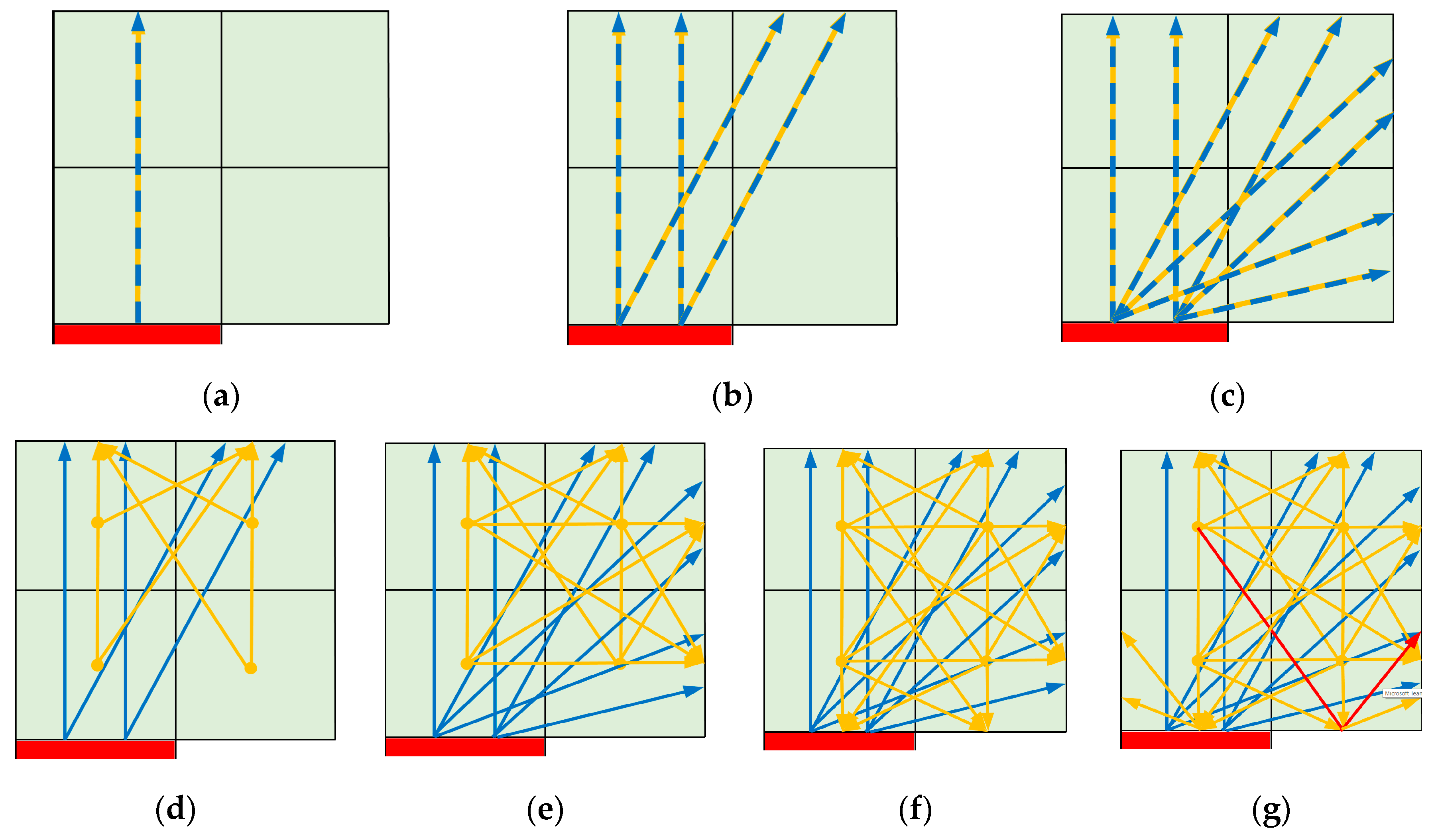
5.1. Different Simulation Setups
We studied seven strategies that describe the propagation of light in the phosphor with different level of approximations, as shown in
Figure 24: 1D propagation only (
Figure 24a) or propagation in multiple directions with a uniform spatial distribution (
Figure 24b–f), as follows:
(a) One general ray goes from the blue chips’ junction in a direction perpendicular to the outer edge of the phosphor. This ray includes decreasing blue flux and the increasing yellow flux.
(b,c) A single general ray or multiple ones may propagate from the junction to each outer surface of the phosphor. The rays include the blue and yellow fluxes. Case (c) covers the full hemisphere, while case (b) covers only the spatial area of the top of the phosphor. This assumption means that the converted light follows the path of the blue light, but in reality, the converted light propagates in all directions.
(d–f) The blue flux corresponds to general rays as assumed in cases (b) and (c), but the yellow light starts from the center of each phosphor cell, taking into account the blue and yellow light absorbed in that cell. The propagation of the yellow light is modeled with uniform spatial distribution. In case (d), the light can propagate only in the direction of the top surface. In case (e), the light goes in the direction of the top surface and the sides, and in case (f), it goes in all directions. When the light reaches the edge of the phosphor, it “disappears”.
(g) Same as (f), but light may be reflected in the selected structures (LED chip, solder, etc.). We always used full reflection in the simulations.
As it can be seen in
Figure 24, even with a small number of cells, the number of possible rays and ray sections is already very high. The full model, shown in
Figure 23, contains 720 blue chip junction cells and 20,628 phosphor cells. Due to the symmetry, we can use half of the model with 360 and 10,314 junction and phosphor cells, respectively. If all rays were taken into account in the calculation, we would have an unmanageable number of rays, especially for yellow rays; therefore, we weight the rays by the estimated flux they carry (i.e., we assign ‘importance’ to them) and sort them by this. The rays with the lowest flux are discarded until the total flux of the remaining rays reaches the desired level. In the simulations presented, we use two
levels of importance: Ninety percent and ninety-nine percent, that is, rays representing 10% and 1% of the flux are discarded. Of course, the discarded flux is distributed proportionally among the remaining rays so the total flux will be finally propagated by the rays considered. The estimated flux transported by a ray is the product of the input flux of the ray and the solid angle,
of the target surface seen from the starting point:
In the case of the half model and five rays per junction, for cases (c), (e), (f), and (g) shown in
Figure 24, the total number of blue rays was 3,663,900. The number of yellow rays was 3,075,078 at a 99% importance level, while at a 90% level it was 1,648,216 only.
Table 3 shows the number of the general (or blue) rays and yellow rays for the different importance levels, the total number of sections of the rays, and the average length of the rays weighted by the estimated flux that they carry.
For the simulations, we used a workstation with an AMD Threadripper 2920x processor having 12 cores and 32 GB of RAM. With this machine, we achieved the following execution times and memory need.
For the half model the simulation of strategy (a), which contains 360 rays, takes 6.9 s and requires 1.0 GB of memory, while strategy (g), with a 90% importance level and nine million rays, takes 435 s and consumes 5.1 GB of RAM. For the full model, strategy (g) with 90% level and 32 million rays, the execution time is 2215 s and memory need is 20.0 GB. Simulating the full model would have required about 80 GB of RAM at a 99% importance level.
In the simulations, the bottom surface of the models was set to a fixed 25 °C, the other sides were modeled with constant convection boundary condition with a heat transfer coefficient of 10 W/m2K, at an ambient temperature of 25 °C.
Based on the findings of A. Alexeev and his co-workers [
48,
49,
50], from the point of view steady-state behavior, the effect of the heat transfer from the top of the phosphor (silicone dome in the case of LED packages with lenses) can be neglected. Therefore, in all simulation scenarios, we neglected radiation—but due to the large, open phosphor surfaces, we assumed cooling by natural convection through the large top surface area of a CoB device. (Alexeev pointed out that in the phosphor, as a secondary heat-path towards the ambient, the heat storage has a significant effect though. Through the thermal capacitance associated with every FVM simulating grid cell, this is inherently accounted for in our thermal simulation model, as it was shown in
Figure 13).
The model parameters used in Equations (21)–(30) contain four phosphor material parameters that were extracted from the measurement results, as outlined earlier. We examined two models:
In one case, we considered that the phosphor absorbs blue light only, allowing yellow to pass completely, i.e., the loss arises exclusively from blue light.
The other model follows the real behavior of the phosphor. It can be seen in
Section 4.4 that the blue and yellow attenuation are approximately equal (
, so the conversion efficiency is also considered to be the same.
Temperature dependency of the parameters is under 0.02%/°C, therefore, it is considered constant in the simulation.
5.2. Influence of the Chosen Light Propagation Model on the Phosphor Temperature
With our modeling approach, the main target was to accurately describe the thermal behavior of white CoB LEDs; the accurate calculation of the distribution of emitted light (i.e., radiance/luminance maps of the CoB surface) was a secondary target for us. Since we cannot measure the temperature distribution inside the phosphor, the question is how accurately the simulated temperature distributions obtained with the simpler models match the results obtained with the most accurate model. To reduce the need for computational resources, we took advantage of the symmetry of the CoB LED device, and only half of the detailed model, shown in
Figure 23, was used. In these simulations, the driving current of the CoB LED was 200 mA, half of the 400 mA of the full model, which resulted in 7.3 W of electrical input power, and the blue flux radiated by the LEDs was 2.5 W.
Table 4 and
Table 5 show the simulation results. We obtained roughly 28% higher phosphor temperature rise with the simplest 1D model (ray strategy (a)) than with the most detailed, most accurate model (ray strategy (g)) while the obtained junction temperatures were practically not affected by the chosen light propagation model.
5.3. Simulated Temperature, Radiance and Luminance Distributions at 400 mA Driving Current, Using Different Phosphor Models
With the models described in the previous sections, steady-state simulations have been carried out for the real CoB device. In all simulations, 400 mA forward current was applied, and we used the phosphor models (a–g) and compared them.
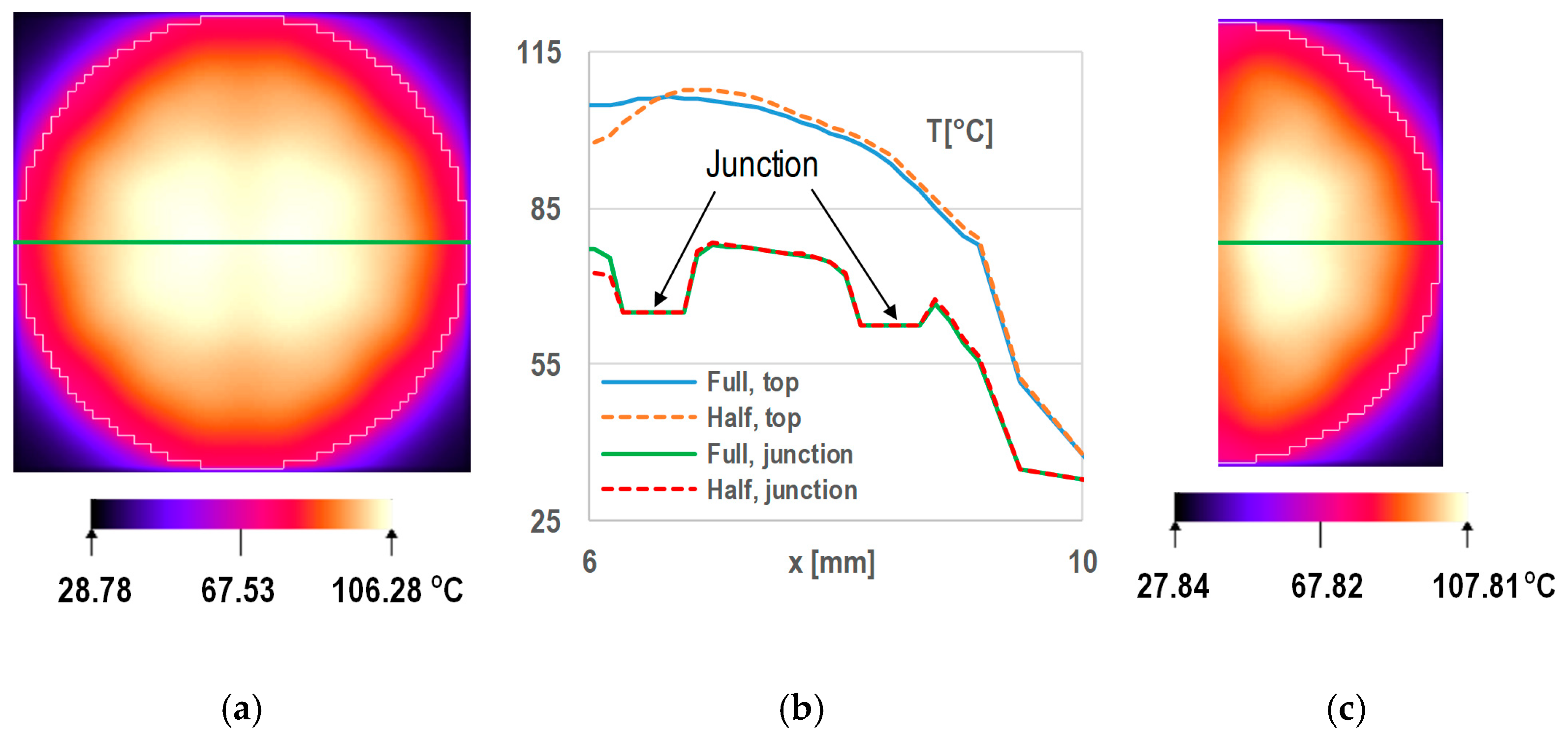
Figure 25 shows the temperature distribution at the top of the CoB LED. Several degrees of differences develop in the temperature distribution obtained by simulating the full and the half structure, see
Figure 25b. At the center of the CoB device, the difference between the results obtained by the full and half models reaches 7.1 °C. The difference obtained for the two structures is due to the different light propagation caused by the symmetry plane as an artificial boundary. The difference in the light propagation can be best visualized by the different distributions of the radiance at the phosphor surface (and also at the internal surfaces of the layered phosphor model) as illustrated in
Figure 26. Thus, this problem can be mitigated to some extent by a modified optical model at the symmetry plane: The cell surfaces in contact with the symmetry plane are also the target surfaces of the rays, and the rays hitting them are reflected on the surface as if coming from the symmetrical other side of the CoB structure such that the total flux of the reflected rays is the same as if the rays would have originated from the missing other half of the structure. This still would result in a somewhat different ray distribution and flux compared to the full model because the rays ‘reflected’ from symmetry plane carry more flux than the rays passing the same plane in the full structure.
Further analysis showed, that even though with the optical model modified at the symmetry plane the radiance distribution of the half model became more similar to the radiance distribution of the full model, but in terms of temperature distribution the deviation of phosphor temperature at the top in the half model was found to be 5.5 °C higher than in the case of simulating the full structure. Overall, taking advantage of the symmetry of the structure to reduce model complexity (which is a common practice in numerical thermal simulations) is not recommended in this multi-domain simulation problem that involves modeling of light propagation as well.
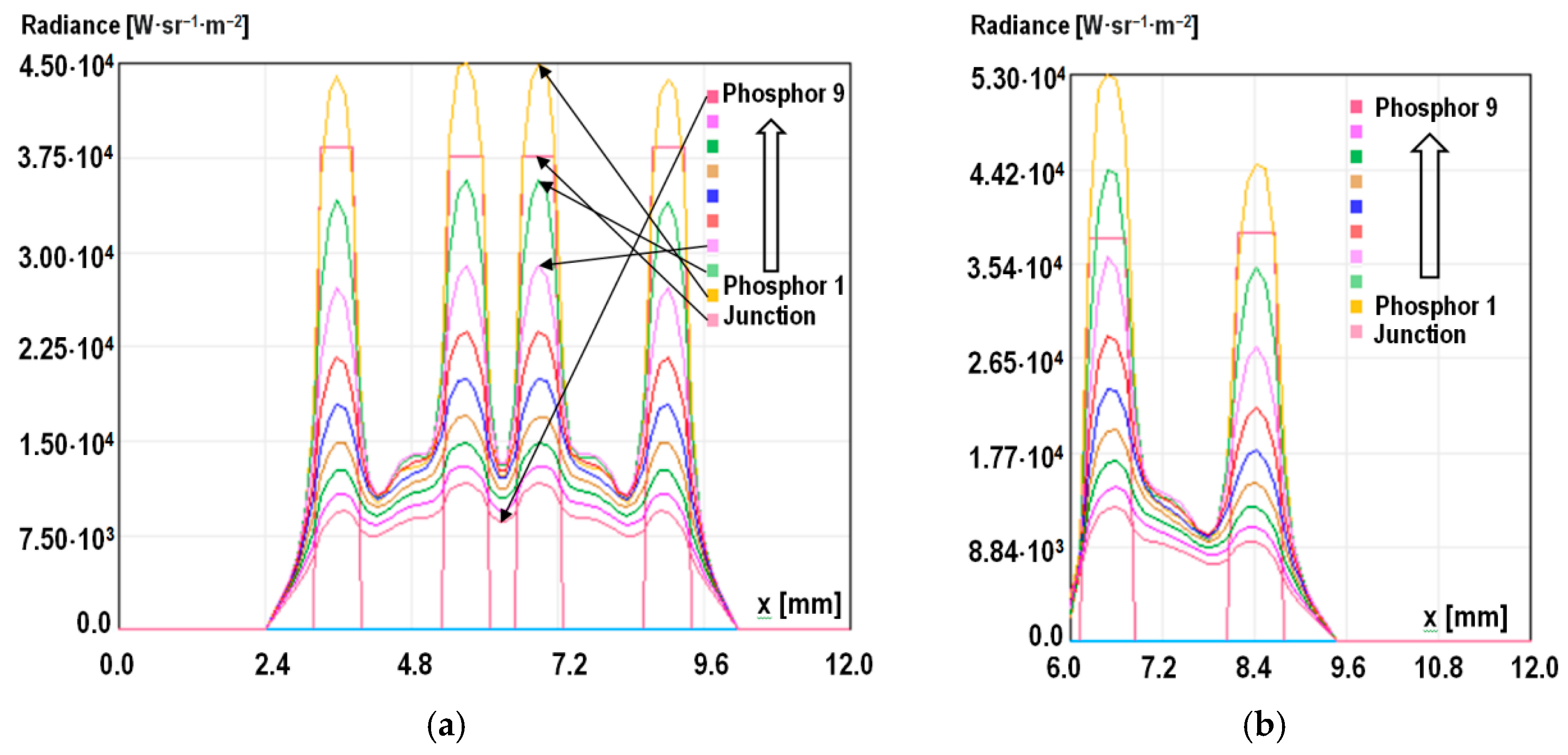
Figure 26 shows that as we move away from the chip, the radiance decreases. The junction layer breaks this pattern, where the radiance is less than in the phosphor layer immediately above it. The reason for this phenomenon is that in the model, the yellow light is reflected from the surface of the chip and does not reach the junction. In
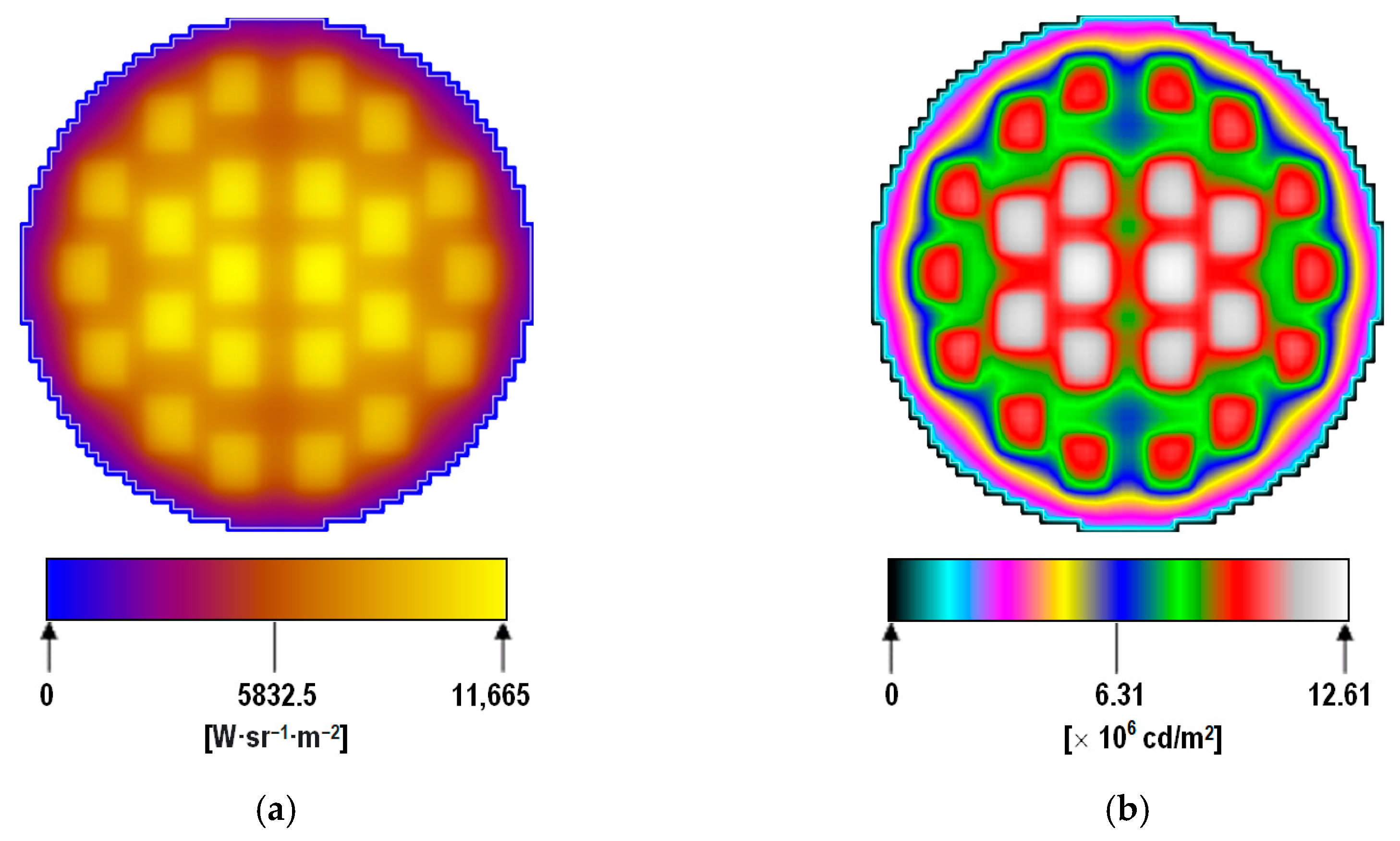
Figure 27, we present simulated radiance and luminance maps at the top of the entire phosphor layer of the CoB device by using the model based on the full geometry of the device structure. (Note, that since in the presented light propagation model the spectral power distribution of the converted light was not resolved, the calculated luminance maps are based on approximated luminous flux values associated with the radiant fluxes carried by the rays, therefore all simulated luminance maps presented here are approximate ones only.)
6. Simulation Results, Comparison with Measurements
The means of comparing the detailed multi-domain simulation results of a CoB device to measured data are very limited. As mentioned in
Section 2, with usual LED package level testing tools, only the ‘ensemble’ characteristics, such as the overall forward voltage and the emitted total radiant or luminous flux can be measured. The junction temperature identified with the help of the JEDEC JESD 51-51 electrical test method for LEDs will also be an average value, without any information about the differences of the individual chip temperatures within a CoB device.
With imaging methods, however, we have some hope to measure properties that we can also obtain by simulations, such as the temperature distribution or the luminance distribution at the top surface of a CoB device, using an infrared camera or an imaging luminance meter (luminance measuring camera). Both measurements are problematic. In the case of infrared thermography, one has to make sure that the emitted light does not introduce false information in the IR image. In the case of luminance measurement cameras, the problem is that such cameras are not designed to characterize high-intensity light sources, when a CoB LED is driven by its nominal forward current, it is so bright that a usual luminance measuring camera gets saturated. Therefore, with such a camera we could measure the luminance distribution of our CoB LED device only at very small forward currents (e.g., 80 mA) where the luminance did not cause the camera to saturate yet. To have a considerable temperature rise, for measurements by an IR camera, the investigated CoB LED was driven by 100 mA forward current. During the measurements the CoB device was attached to a temperature-controlled stage, providing a targeted ambient temperature of 25 °C (in practice achieving an actual temperature of 24.4 °C).
During the simulations an ambient temperature of 25 °C was assumed, the thermal boundary conditions were the following: At the bottom of the ceramics substrate of the CoB structure, we assumed a 25 °C constant temperature; while at the other outer surfaces of the device (at the sides and at the top), a heat transfer coefficient of 10 W/m
2K was applied (representing heat transfer by natural convection roughly). In
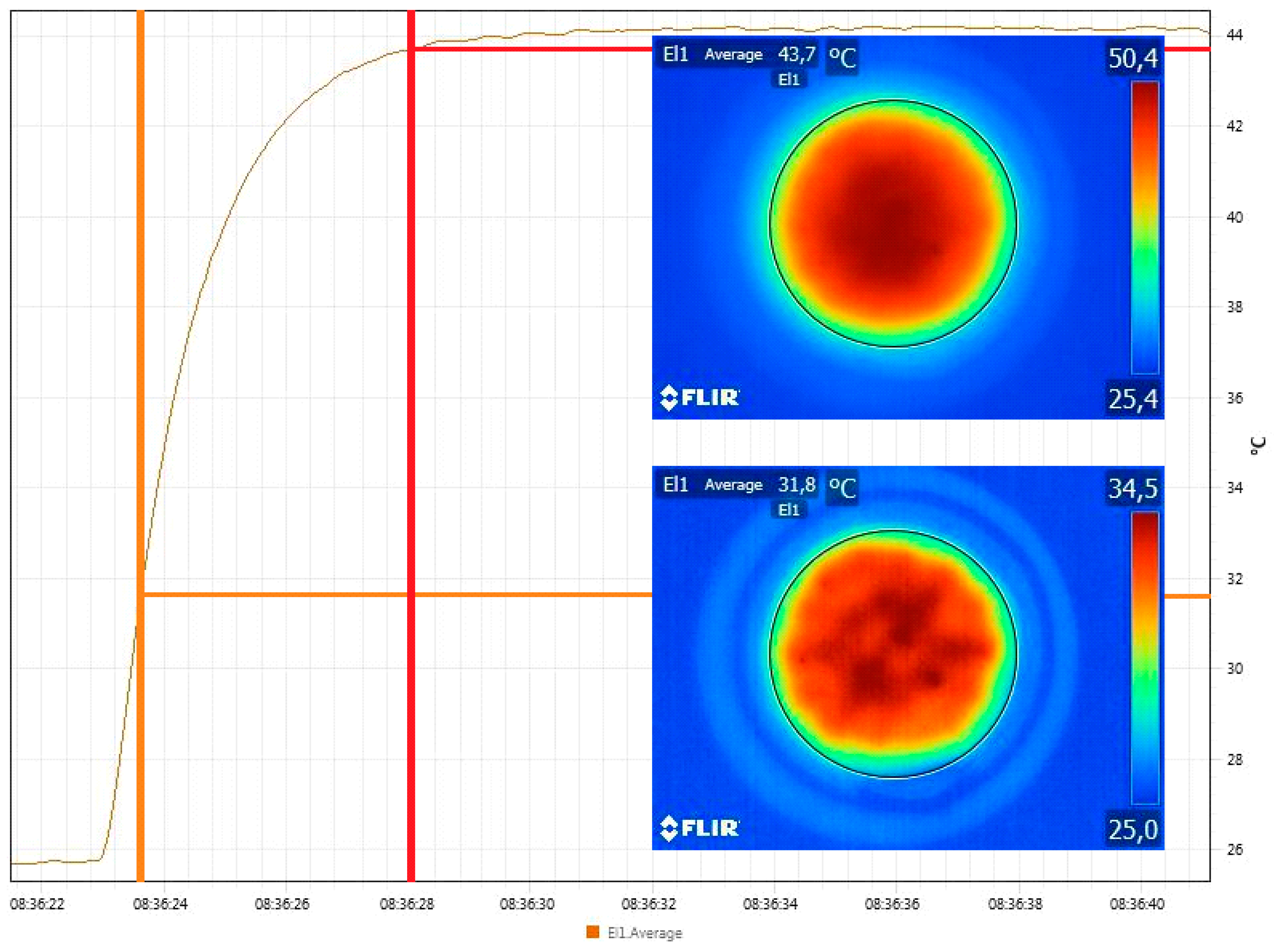
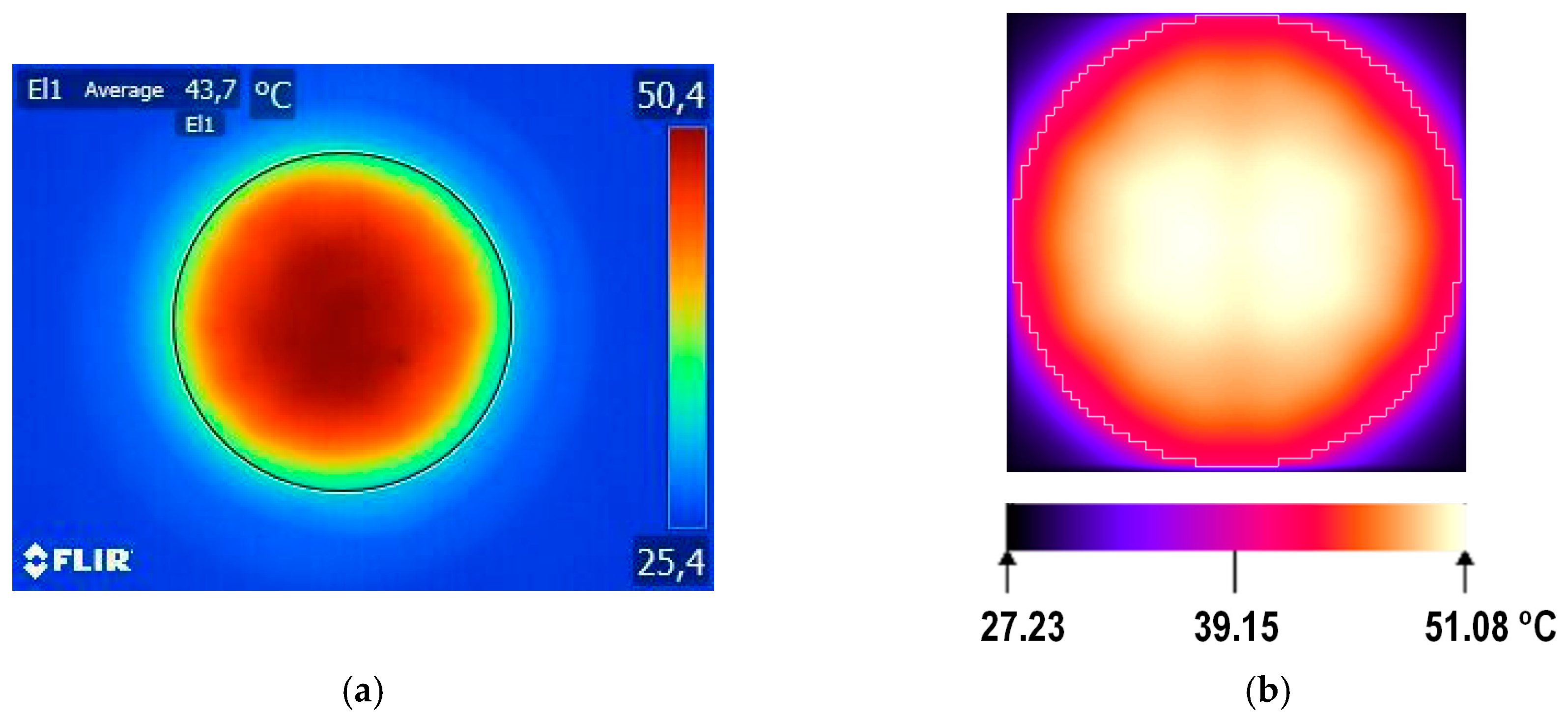
Figure 28, we present the transient of the average temperature of the CoB device together with two temperature maps grabbed during the heating up process. The image on the top corresponding to 43.7 °C average temperature represents already the thermal quasi-steady-state of the device. This is compared to the simulated surface temperature distribution in
Figure 29: The peak temperature and the shape of the temperature distribution are well estimated by the simulation, the difference in the measured and simulated peak temperature is 0.68 °C only.
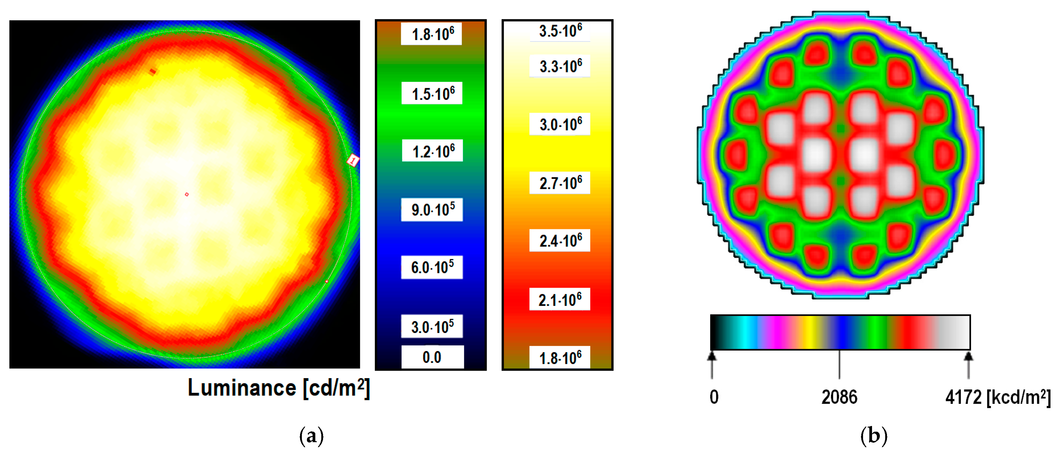
Comparing the measured and simulated luminance maps (
Figure 30) we can see that the difference between the measured and simulated maximal luminance is 19% while in the average luminance the difference is 7% (measured—2.721 × 10
6 cd/m
2, simulated—2.528 × 10
6 cd/m
2). One reason for the higher maximum simulated luminance value is the 90% importance level (meaning that 10% of the radiated power was distributed among the major light paths). We could not apply a higher importance level on the available computers. Another probable reason for the discrepancy is that there may be differences in the actual internal structure of the CoB LED compared to the modeled structure, and the actual reflections may differ from the ideal case used in the model.
Note, that at this stage of the development of our FVM simulation model, it is very hard to judge the accuracy of the simulations from the differences between the measured and simulated luminance maps. On the one hand, even at the low driving currents the CoB LED device was too bright for accurate direct imaging with the luminance measuring camera; on the other hand, due to the lack of resolving the spectral power distribution of the converted light in the optical part of our multi-domain model, the luminance estimated from the radiance is only a very rough approximation. Nevertheless, the properly matching orders of magnitude of the simulated and measured luminance values obtained for the brightest spots and the 19% relative difference between maximal values and 7% difference between average values are promising.
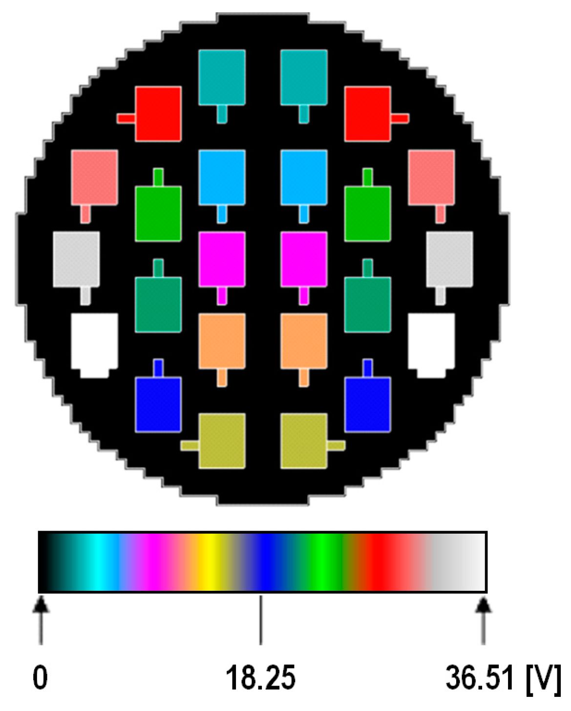
A further result from the multi-domain simulations of the CoB device is the voltage distribution on the chip interconnect metallization layers, see
Figure 31. The differences between the discrete values corresponding to the chip locations represent the actual forward voltages of the individual chips, calculated by the instances of the chip-level multi-domain LED model, embedded into our FVM solver. The actual voltage drops are determined by the local temperatures of the chips. Unlike in the case of a real, physical CoB device, in the simulation model, we have access to the individual forward voltage values of the chips, present in the LED array of a CoB device.
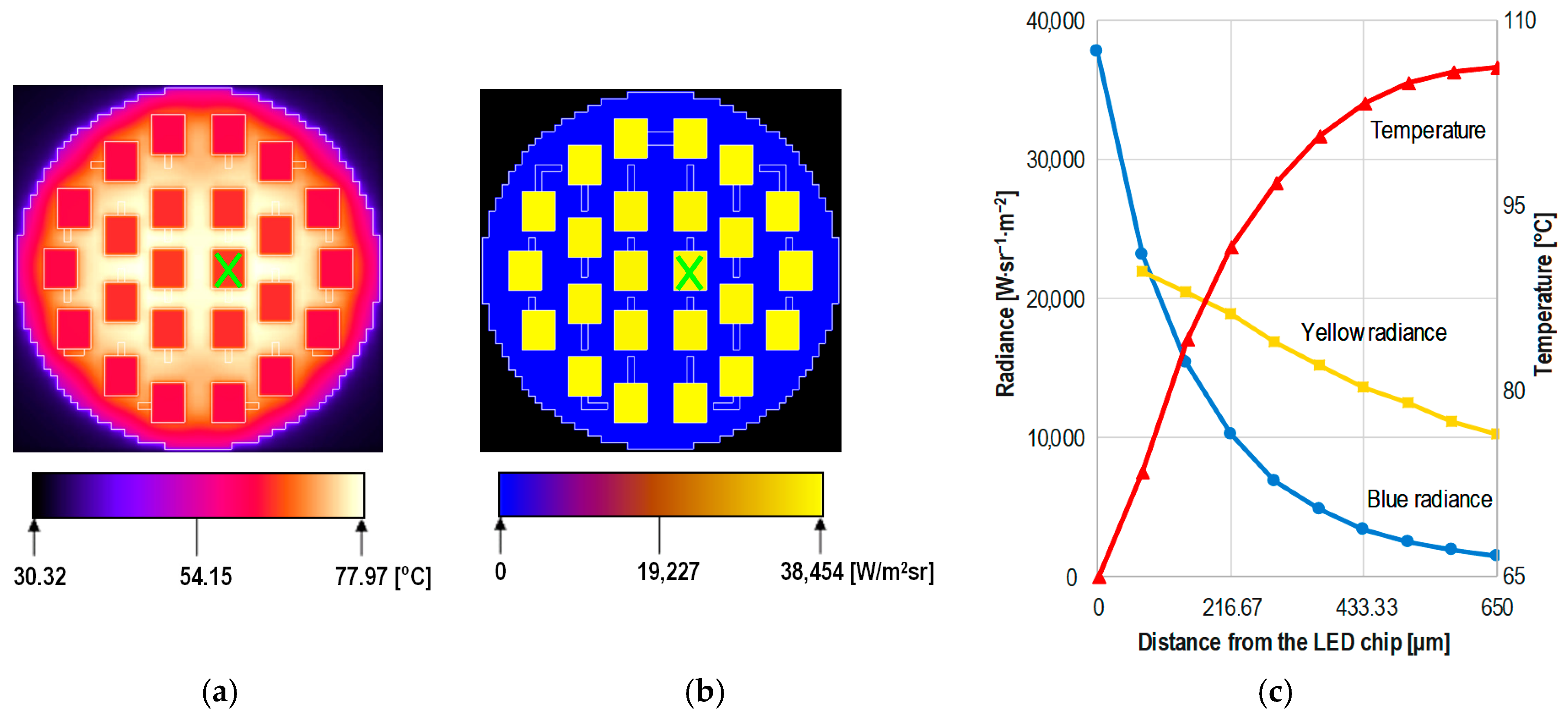
The simulation also provides insight into the lateral and vertical distributions of other properties, such as the actual junction temperatures of the individual LED chips, radiance at a given plane within the phosphor parallel to the substrate, phosphor temperature as a function of distance from the blue chip surfaces, as illustrated in
Figure 32.
Note that, a similar vertical characteristic was published in [
23] where the yellow light continuously increases away from the junction, while in
Figure 32c it decreases continuously. The phenomenon is caused by the difference between the two light propagation models: In Reference [
23] propagation model (a) was used where blue and yellow light travel together, perpendicular to the chip surface, while
Figure 32c corresponds to the light propagation model (g) where the yellow light exits the cells of the phosphor model with equal probability in all directions, so a significant portion of it starts down, then it is reflected from the surface of the chip and travels towards the surface of the phosphor. This means that the yellow light passes through many surfaces in both directions. The consequence of this phenomenon is that there is greater radiance near the chip and dissipation occurs closer to the chip than in the case of applying model (a), resulting in a lower average phosphor temperature.
As mentioned before, one cannot compare the simulated internal distributions of the forward voltages, chip junction temperatures and vertical phosphor temperature distributions to measurements, the ‘ensemble’ characteristics though, such as the overall forward voltage or the emitted total radiant flux can be both measured and calculated from the simulation results. In
Table 6, we provide a comparison of these quantities.
Table 6 also provides temperature data: The ‘ensemble’ junction temperature,
as measured in compliance with the JEDEC JESD51-51/51-52 standards and an average junction temperature,
, calculated from the distinct junction temperatures used as input to the instances of the multi-domain chip-level LED compact model. Since these temperature values are obtained in different ways, it does not make sense to calculate any relative temperature error from them.
7. Summary and Conclusions
In this paper, we proposed and described a methodology for electrical-thermal-radiometric multi-domain modeling and simulation of white CoB LEDs by the combination of compact and distributed modeling methods.
We have also presented a method for multi-domain light modeling in the phosphor, also considering the local temperature dependence of some phosphor properties, such as the conversion efficiency. We implemented different physics/analytic formulae based light propagation models of various complexities and with a few, added heuristics, offering different trade-offs between the need for computational resources and expected accuracy.
A major bottleneck in every numerical simulation is to provide accurate/realistic input data, especially in terms of material properties. Phosphor layers in LEDs pose special problems in this regard, since the composition of the applied materials are usually not disclosed to the public, not even general data, such as thermal conductivity or exact absorption/emission spectra and their possible temperature dependence. Therefore, in order to set up realistic models, we created our own phosphor samples and our own phosphor-converted white LEDs that were characterized in details, in order to extract the phosphor properties as input for modeling and also, to serve as simple reference structures with controlled properties for validating our simulation models.
With the developed opto-thermal model for phosphor layers we carried out trial simulations for assumed CoB LED structures with different phosphor thicknesses, and with these models we also compared our different light propagation models. We found that for single-chip white LEDs with thin phosphor layers, even the simplest 1D light propagation model may provide sufficiently accurate results. For a general case of any complex CoB device, however, we found that the complex 3D light propagation model is better suited. We found that certain heuristics can be used to speed up the simulations without compromising the accuracy of the results. This 3D light propagation model was implemented in our FVM based numerical simulation code. With our previously proposed Spice-like chip-level multi-domain LED model included, the electrical behavior of the LED chips is also included in the CoB model, allowing to study different chip-level, package level and phosphor level problems (such as the effect of increased local junction heating, due to thermally degraded die attach layers on the luminous flux output) simultaneously, spatially resolved to chip-level or even to smaller scales.
The use of this detailed, distributed thermo-optical model, combined with the LED chips’ compact multi-domain model, was demonstrated through the example of the Lumileds 1202s CoB LED devices. This was among the test samples of the round-robin test of the Delphi4LED project and such was already characterized in great detail by multiple independent LED testing laboratories [
43]. Using this example, we found that our present modeling approach provides satisfactory accuracy during multi-domain simulation of CoB devices.
The work reported here is far from complete. An obvious approximation is that the spectral power distribution of the converted light is not yet considered. This issue, though, does not impose any theoretical problem; only the ‘yellow ray model’, indicated in
Figure 17, needs to be multiplied according to the number of spectral ranges to which the detailed emission spectrum of the converted light is resolved. This would be important to model the visual performance (such as the total luminous flux, the surface luminance map, color point/correlated color temperature) of the CoB devices accurately enough. Note, however, that in terms of calculations of the radiant properties, our present model already provides accurate results since in the calculation of the yellow photon number the wavelength dependence of the radiant power of the photon flux is considered.


