Abstract
In view of their applicability in optoelectronics, we review here the relevant structural, electronic, and optical features of the inorganic Pb-free halide perovskite class. In particular, after discussing the reasons that have motivated their introduction in opposition to their more widely investigated organic-inorganic counterparts, we highlight milestones already achieved in their synthesis and characterization and show how the use of ab initio ground and excited state methods is relevant in predicting their properties and in disclosing yet unsolved issues which characterize both ternary and quaternary stoichiometry double-perovskites.
1. Introduction
In the last decade the community has literally faced a novel gold rush towards a new class of materials that has revolutionized the scenario of low-cost photovoltaics (PV): the bulk hybrid organic-inorganic halide perovskites (OIHPs) [1] described by the general stoichiometric relationship ABX (A = organic cation; B = Pb, Sn, Ge; X = halide). OIHPs, whose lead compound is MAPbI (MA = CHNH), have been indeed applied as light harvesters with astonishing and unprecedented photo-conversion efficiencies (PCEs) that recently passed 25% [2]. This success is ascribed to their relevant characteristics for PV applications, such as a bandgap close to the ideal value for single-junction solar devices [3], excellent compatibility with solution-based processing (cheap synthesis of the material), a very long carrier diffusion length [4,5], and the ambipolar nature of their carriers (see among the others [6,7,8,9,10,11]). Aiming at disclosing the properties and the potentialities of OIHPs in PV, several efforts have been jointly made by the theoretical and experimental community [12,13,14], and certainly it can be stated that most of the material properties have been fully characterized. Anyway, detrimental issues still afflict the mass production of the so called perovskite solar cells (PSCs). Among them and of particular relevance are the presence of hysteresis in the J-V curve, the instability towards heat and moisture, and not secondarily, the presence of Pb, toxic element par excellence. Hysteresis is a well-known issue [15] that has mainly affected MAPbI PSCs [16] which is associated with slow dynamic reorganization processes, and that has been ascribed to three main factors; i.e., the large permanent dipole moment MA cation rotation inside the lead halide cavity [17], the ferroelectric polarization (quite unlikely [18]) of the material, and also due to the ionic migration once the bias is applied [19,20,21]. More recently, the ionic migration mechanism has been partly discarded [22], while the possible formation of alloys between MA and other cations with reduced dipole moment (mainly formamidinium (FA = HC(NH)), and guanidinium (GA = C(NH)) has been shown to be extremely beneficial in reducing hysteresis of the J-V curve, as initially predicted by some of us [17], even if the bulkier structure of cations other than MA [23] places them preferentially at the interface and/or at the boundaries [24,25,26,27] (and not in the perovskite A-site), with the final result of highly improving the performances of the devices [28,29]. While hysteresis is clearly more related to the final application of the material in solar cells (some architectures are more prone than others to hysteresis), the other issues are intrinsic, and in this sense, the material, more than the architecture, needs to be engineered. The instability towards moisture, essentially due to the presence of the short hydrophilic and volatile cation MA, Ref. [30] has been matter of analysis both at the experimental [31] and the theoretical level [32]. The most plausible and intuitive solution of said issue is the partial/total replacement of MA with longer, hydrophobic, organic cations. In this direction there is the synthesis of mixed 2D/3D or pure 2D hybrid perovskites, also known as Ruddlesden–Popper [33,34] and Dion–Jacobsen [35] hybrid perovskites. The initial efforts on these materials are certainly due to the work of David Mitzi who, in the middle of 90s, investigated this class, as a function of the organic cation length, for its possible applications in optoelectronics [36,37,38]. Only more recently, in 2014, the group of Karunadasa, in Stanford, revealed the stability and the suitability of a layered Pb–I perovskite as a solar-cell absorber. In particular, they report for a n = 3 (n = 1 is pure 2D; n = ∞ is 3D bulk MAPbI) system (PEA)(MA)PbI (here PEA, phenethylammonium, CH(CH)NH, is the organic-spacer between three layers of MAPbI (see Figure 1)) a PCE of 4.73% [39].
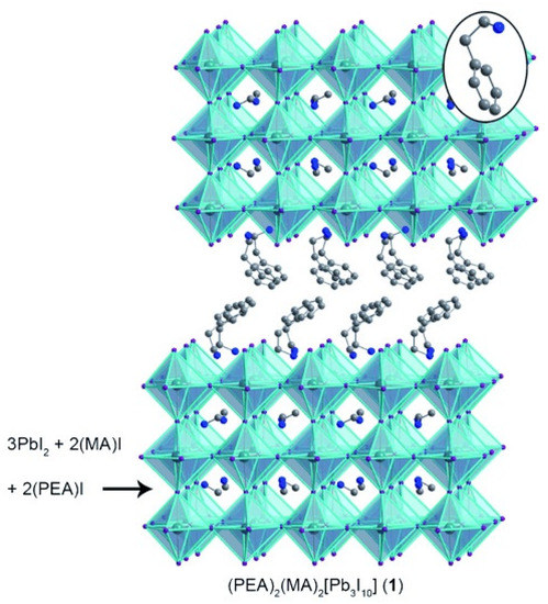
Figure 1.
2D perovskite (PEA)(MA)[PbI] (1). The inorganic layers in 1 can be structurally derived from MAPbI by slicing along specific crystallographic planes. Inset: a PEA cation in the organic layers. Atom colors: Pb = turquoise; I = purple; N = blue; C = gray. Disordered atoms and hydrogens omitted for clarity. (Reprinted with permission from [39]. Copyright 2014 WILEY-VCH Verlag GmbH and Co. KGaA, Weinheim).
Phenethylammonium and buthylammonium (BA = CH(CH)NH) are the two spacers [40], aromatic and aliphatic, present in these 2D and 2D/3D mixed systems. The encouraging results have boosted the research in such field. In particular, the group of Kanatzidis [33] has systematically investigated synthetic paths and optical properties of n= 1–4 terms of the series in (CH(CH)NH)(CHNH)PbI, finding that the thickness is controllable by tuning the ratio between the spacer and the short chain organic cations. Additionally, strong photoluminescence (PL) that suggests their usage in LED has been revealed for lower n members, while, following the corresponding bandgap, higher n members can be used as efficient light absorbers in solar devices. The stability of such devices has been clearly demonstrated [34]. Our recent research has focused on the theoretical investigation of the first two members of the series (n = 1,2) in the case of (BA)(MA)PbI compound [41]. Particular attention has been paid to the study of the electronic and optical properties. In detail, we have calculated the quasiparticle (QP) energies in the GW approximation and the optical excitation energies solving the Bethe–Salpeter equation (BSE). Our results support the fact that higher values of n provide materials more suitable for PV, having quite spatially delocalized excitons, while pure 2D systems (n = 1) are characterized by strongly localized e-h couples compatible with the high PL observed experimentally and thus more suitable for LED.
The last and probably most detrimental issue is environmental and stems from the presence in OIHPs of lead (Pb). The moisture mediated degradation of bulk OIHPs further enhances the risk of Pb dispersion in the environment. To fix said issue, the community has initially paid attention to the most logical alternative; i.e., the replacement of Pb, partial or total, with elements belonging to same group (IV)—i.e., Ge [42,43] and Sn [44,45]. Alternatively, a heterovalent replacement of Pb atom pairs with a +1/+3 atom couple has been suggested [46] as a viable alternative. All such alternatives, even if potentially providing good conversions, at the same time remain unstable due to the presence of the organic part. A possible candidate is, then, a fully-inorganic halide perovskite, where the organic moiety is replaced by an inorganic one, and lead by a metal (in homo- or heterovalent fashion). In other words, it is just like following the tracks back to the parental compound (CsPbX, X = halide) from where, initially, the archetypal hybrid compound, MAPbI was synthesized the first time by Weber in 1978 [47,48], and moving from CsPbX, properly substitute Pb with safer elements. This process can take place in two ways. As for the case of OIHPs, the first and more straightforward one is replacing Pb with other divalent cations, such as Sn, which, anyway, show a more marked tendency to oxidize (Sn evolves towards Sn [49]). The second process, also known as atomic transmutation, involves the substitution of Pb pairs with two ions in the and oxidation states, respectively. Such a “tailored” approach has already opened the way to the synthesis of novel materials; e.g., CuGaSe (chalcopyrite, E = 1.7 eV) and CuZnSnSe (kesterite, E = 1.0 eV), ternary and quaternary derivatives of the parental ZnSe (following the two subsequent 2 Zn⟶ Cu + Ga, and 2 Ga⟶ Zn + Sn substitutions, respectively) [50,51,52]. While quaternary (heterovalent replacement of Pb with two different ions, and oxidation states, AB(I)B(III)X) inorganic perovskites have been deeply investigated, less attention has been paid to the ternary (homovalent substitution with one single atom, assuming both and oxidation state in the final compound, AB(I)B(III)X) perovskites. In this context, in the last few years we contributed to the study of a potential alternative to Pb-based inorganic perovskites based both on ternary [53] and quaternary double-perovskites [54].
We aim now to remember the general conditions of the existence of a perovskite crystalline structure. While for the organic-inorganic class, a tolerance factor concept has been extended in order to take into account the molecular nature of the organic cation [23,55], the pure inorganic halide perovskites refer to the classical concept of tolerance (t) initially developed for oxides by Goldschmidt in 1926 [56] and later extended to other classes. The perovskite is stable when the relationship:
(, , and are radii of A, B, and X-site atoms) provides values close to unity. Ideal cubic perovskite (t = 1) is the case for SrTiO. Lower values of t (0.89–1) still ensure the cubic symmetry, while t < 0.89 leads to orthorhombic arrangement of the perovskite structure. Even lower values (t < 0.71) are associated with close-packed structures such as those characterizing ilmenite or corundum [57]. On the other hand, t > 1 other geometries prevail, including hexagonal to other 2D-like ones [11]. The other parameter to be kept in mind in order to assess the formability of the perovskite geometry (also for halide case) is the octahedral factor () that is defined as:
With this in mind, in the following, we review some of the main results concerning the two classes of materials, i.e., Pb–free double-perovskites with ternary and quaternary stoichiometry, while focusing on performances and possible applications in optoelectronics.
2. Ternary Perovskites
Moving from the most studied ternary inorganic halide perovskite, CsPbI, it is straightforward to first discuss other group-IV ternary halides, CsMX (M = Ge(II), Sn(II); X = halides).
2.1. Sn Halide Perovskites
At the very beginning of the perovskite "fever," few groups focused, theoretically [58,59] and experimentally [60], on the structural properties of CsMX. Kanatzidis and his group, by means of a combined experimental/theoretical approach, have focused [60] on the polymorphism of CsSnI observing a rapid phase transition (after heat/air exposure) between two polymorphs, at room temperature. The orthorhombic black (B-) CsSnI characterized by a bandgap of 1.3 eV is a p-type semiconductor, while the other room-temperature polymorph, the yellow (Y) one, has a bandgap which is twice (2.55 eV) that of the (B-). (Figure 2 shows polymorphism of CsSnI and details of phase transitions).
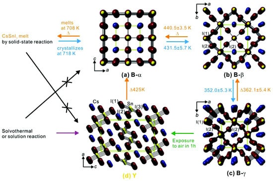
Figure 2.
Illustration of phase change details of four CsSnI polymorphs and their crystal structures. How phase transitions of CsSnI polymorphs proceed is displayed with synthesis conditions and conversion temperatures obtained by in situ, temperature-dependent synchrotron powder XRD studies. Crystal structures of the respective polymorphs are shown: (a) black cubic (B-) at 500 K; (b) tetragonal (B-) at 380 K; (c) orthorhombic (B-) at 300 K; (d) yellow (Y) phase at 300 K. Disordered atoms in (c) are omitted for clarity. Cs atoms, blue; Sn atoms, yellow; I atoms, violet. Green dashed lines represent a unit cell. (Reproduced with permission from [60]. Copyright (2012) American Chemical Society.)
Very uniquely, the latter polymorph shows both strong PL (at 950 nm, near IR) and high electrical conductivity with a further high mobility, quite an unusual feature in such a class of compounds, associated with a noticeably high tendency of Sn-vacancy formation. A material with such appealing features is thus a "clean" potential alternative to GaAs and CdTe in optical amplifiers, in fiber-optic systems for telecommunications, in tunable solid-state laser systems, and in biomedical applications. Said peculiarity of having a high electrical conductivity along with a high mobility of holes made possible the usage of CsSnI as a hole transport material (HTM) in dye sensitized solar cells (DSSCs) accompanied with relevant performances (PCE ∼10%) [61]. There remain, anyway, issues in the applications of black CsSnI as a solar harvester in perovskite solar devices due to the degradability in air, a feature that characterizes all Sn-based, hybrid, and fully-inorganic, perovskites [49]. A good alternative is the usage of CsSnI, a defect variant of the parental perovskite (half of the octahedral Sn are missing) that contains Sn instead of Sn. Said material offers an intriguing alternative to black CsSnI because its enhanced stability and bandgap are ideal for solar single-junction devices: Qiu et al. have measured an optical bandgap of 1.48 eV (PL), while finding also a high absorption coefficient (>10 cm) [62]. The same authors obtained an encouraging preliminary PCE of 0.96% for cells using CsSnI as the harvester (N-i-P architecture). (J = 5.41 mA cm; V = 0.51 V; FF = 0.35). On the other hand, the CsSnX-quantum dots (QD) (for all-inorganic perovskite QDs we refer the readers to more specific papers [63,64]) allow for improved chemical stabilization, increased quantum confinement, and larger exciton binding energies. The addition of triphenyl phosphite [65] as an antioxidant agent further extends the life of the device that reaches PCE > 5%, so far the highest performance for Pb-free inorganic perovskite solar cells. The material remains, anyway, extremely tricky since the understanding of its properties is a bit elusive, a condition that limits its usage in PSC. In this sense the contribution of theoreticians has been (and still is) fundamental in better shedding light in the knowledge of the basic properties of CsSnI. By means of a combined DFT and approach, Even and his group have characterized the phase transition path of Sn-/Pb-halides, both inorganic and hybrid, thereby reporting the impactful role of relativistic effects (SOC) to be quantitatively larger than that of strain [66]. A splitting in the conduction band due to SOC is indeed 0.4 eV, a value, as stated, significantly larger than that from the strain.
CsSnBr is the other most investigated tin-based cesium halide. Its most stable polymorph at room temperature has cubic symmetry [67,68] even if orthorhombic (Pnma) and tetragonal (P) phases are similarly detected as lower temperature polymorphs [69]. Interestingly, for said compound Fabini et al. discussed the appearance of a so-called emphanisis; i.e., a phenomenon associated with the appearance upon warming of a locally distorted state. It is due to the presence of a 5s lone pair being accompanied by an off-centering of Sn ion, and it is more marked in the case of Sn, (in Pb the same effect is counterbalanced by relativistic effects that stabilize the lone pair). The Sn displacements are likely to induce a splitting of the otherwise degenerate conduction band minimum (CBM), thereby possibly reducing the carrier recombination, a recombination that is potentially reduced by the formation of large polarons still associated with the enhanced lattice deformability induced by the off-center tendency of Sn. PL measurements show rapid blue-shift of the gap upon warming, revealing, thus, an anomalous evolution of the gap as function of the temperature. One of the main roles played by CsSnBr is the fact that it "cubizes" the otherwise orthorhombic CsSnI (Table 1 collects the main available data concerning structural, electronic, optical, and PV device-oriented properties of the ternary single and double-perovskites discussed in the text). This enhances the suitability of the resulting CsSnIBr alloys for optoelectronics, allowing for a wider gap tunability. In particular, the optical bandgap of the perovskite increases by 38.5% with a blueshift in the absorption spectra when I is progressively replaced by Br [70]. In detail, the optical bandgap onset ranges from 1.27 eV (CsSnI) to 1.73 eV (CsSnBr), passing through two intermediate values; i.e., 1.37 eV (CsSnIBr) and 1.65 eV (CsSnIBr), respectively. Similarly, alloying with CsSnBr has the advantage of enhancing the otherwise low value of the open-circuit voltage for pure CsSnI compounds: 2.30 mV for pure CsSnI, 190 mV for CsSnBr, up to 410 mV for CsSnBr in the presence of SnF. SnF plays the role of making closer the perovskite valence band maximum (VBM) with the highest occupied molecular orbital (HOMO) of the hole transport material. CsSnBr-based devices with (20% mol) and without SnF show PCE = 2.17% and 0.01%, respectively. In contrast, devices based on bare CsSnI are characterized by poor performances (PCE = 3.0 × 10) [70].

Table 1.
Main structural, electronic, optical, and PV properties of the 3D ternary single and double-perovskites discussed in the text. In the first column, the species and the crystal symmetry is reported (for CsGeI, L and H are low and high-temperature polymorphs, respectively) In the second, both theoretical (in parenthesis the level of theory) and experimental values of the lattice parameters are reported. The third column contains the bandgap, theoretical (still in parenthesis the level of calculation) and experimental (in parenthesis the experimental methodology Absorption/Reflectivity and Photoluminescence). The direct (d) and the indirect (i) nature of the gap is similarly reported. The fourth column contains available PV parameters, i.e., the short-circuit current (J), the open-circuit voltage (V), the fill factor (FF), and the Photoconversion Efficiency ()
2.2. Ge Halide Perovskites
The second most natural choice for Pb replacing is Ge. Among the three pure halides (X = Cl, I, Br), CsGeI is the most investigated compound. In a combined theoretical and experimental approach, Krishnamoorthy et al. [71] have studied the properties of this material as solar harvester, obtaining solar cells characterized by a PCE of 0.11% (J = 5.7 mA cm; V = 74 mV; FF = 27%). They similarly have determined that it crystallizes in a stable rhombohedral structure (without any phase change in the device’s working temperature). Du et al. [72], by means of a density functional theory-based approach, have investigated the dielectric properties of the material, revealing its large static dielectric constant, and interestingly the fact that it can work as an HTM in dye-sensitized solar cells better than CsSnI because of a better band-edge alignment. Indeed, using the vacuum level as reference, the VBM of CsGeI (−5.1 eV [71]) results in a lower energy than that of CsSnI (−4.92 eV [61]), and accordingly, is closer in energy to the dye (in this case N719) HOMO (−6.01 eV [61]). Because of such alignment, the hole more easily could pass from the dye to CsGeI HTM. CsGeI seems to have also a favorable alignment when used as an HTM in PSC (with MAPbI as solar harvester). The only caveat, in this case, can be represented by the inverted architecture: here the photons passing first through the HTM, are adsorbed by CsGeI and deep iodine vacancies may be formed (low formation energy defect) with a detrimental effect for the final working principle of the inverted device. Still on the theoretical side, Roknuzzaman et al. [73], following a combined mechanical/optical properties analysis based on a DFT hybrid functional approach, have reported the better suitability (enhanced ductility) of CsGe(IBr), over the initial CsGeI. Additionally, Nakajima et al. [74] report a bandgap for CsGeBr of 1.56 eV (SOC/HSE12 [75]), a value that perfectly matches with the one required by an ideal single-junction device [76].
2.3. Bi and Other Halide Perovskites
With a difference in the ionic radius of only 0.16 Å (1.03 vs. 1.19 Å [77]), bismuth is other optimal candidate for replacing Pb in halide perovskites. Its choice would seem a natural consequence also of the very close electronic configuration between the ions; Bi and Pb are indeed isoelectronic (same 6s lone pair). Having said that, it is straightforward that different dimensionalities characterize Bi perovskites because of the different valences of bismuth and lead. XRD experiments showed that a 2D pattern characterizes the quite unusual CsBiI compound [78] with a bandgap of 1.77 eV. PV devices assembled using this harvester provide the best J of 3.4 mA cm and V = 0.31 V for a CsI:BiI precursor molar ratio 1:3. (FF = 0.38) [79]. The J value reported is quite high, while V is lower than values reported (2.15 mA cm and 0.85 V, FF = 0.60, respectively) for the other most investigated Bi-based halide perovskite [80], i.e., CsBiI [81], as a result of the broader light absorption spectrum of the former with an extended absorption of light at longer wavelengths compared with solar devices based on this latter compound. Similarly to CsBiI, CsBiI (whose bandgap is larger, 2.03 eV) is characterized by a layered structure, even if it has different growing directions. In the ABiI stoichiometry, bi-octahedral (BiI) clusters are surrounded by Cs cations [80] in a hexagonal phase. Devices based on these two materials are characterized by enhanced stability [82,83]. CsBiX nanocrystals (NCs) are further characterized by large photo-luminescence quantum yield (PLQY) as well. Quantum dots (QDs) of CsBiI were synthesized by using oleic acid and octylammonium bromide for ligand binding and characterized by a PLQY of 22%, (∼110 times larger than that of the reported ligand-free CsBiBr QDs). Heating up to 180 C for 1 h does not alter these appealing features. CsBiCl and CsBiI QDs are characterized by encouraging fluorescence properties, (PLQYs of 62% and 2.3%, respectively), demonstrating the tunability of emission in the 380 to 526 nm range [84]. An interesting experimental/theoretical paper by Maughan et al. [85] has focused on the cubic, vacancy-ordered double perovskite structure (F) CsTeI by comparing its properties with those of the +4 Sn, CsSnI, and similarly investigating the properties of their alloys, CsSnTeI. The experimental optical bandgap for CsTeI (CsSnI) is ∼1.59 (1.25) eV, with the optical gap determination for the former complicated by the presence of exciton-like features near the absorption edge, which are ascribed to the Te(IV) 5s electron configuration (single-ion excited states). No data have been reported about the properties of CsTeI and the alloys in devices. It is, anyway, interesting to underline the intolerance of CsTeI for forming defects. This is attributed to the enhanced covalency of Te–I bond (iodine vacancies are unlikely to form) which raises the energy of the conduction band. (Larger gaps, with defects, enhanced the possibility of the defects lying in the gap: this feature does not apply to CsSnI, whose bandgap is smaller than that of CsTeI.) In analogy with CsMX (M = Sn, Te), Ju et al. [86] have combined a theoretical (DFT calculations) and experimental approach (XRD) in order to investigate earth-abundant, nontoxic, and stable CsTiIBr (x = 0, 2, 4, 6) halide perovskites, finding that the combinations with x = 0 and x = 2 (E = 1.38 and 1.78 eV, respectively) are ideal candidates for applications in single-junction PSCs and tandem devices. Said class seems, furthermore, more affordable than noble-metal-based ternary compounds such as CsPdBr [87], which, anyway, has been demonstrated to have a good moisture (water) resistance, long-lived PL, a bandgap of 1.6 eV, and reasonably dispersive bands. A further class of ternary inorganic perovskites that has been recently investigated is represented by alkali earth metal ions in the B site of the perovskite CsMX (here M = alkali earth ions; X = halides) [88] and its interactions with rare earth metals, both as dopants and in alloys, the latter with interesting applicability as scintillators [89]. Among the others, the PL properties of such mixed systems were studied for Eu [90,91] and for Yb [92].
2.4. Ternary Halide Double-Perovskites
Finally, we aim here to discuss the properties of CsAuX (X = Cl, Br, I) or better, CsAuX, according to the formal two-fold oxidation state of Au in such compounds (similar behavior has recently been discussed for Tl atoms [93]). This is not a very recently synthesized compound, since the first works focusing on its analysis, are dated to the beginning of the 70s. In their paper, Brauer and Sleater [94] described, indeed, the preparation of mixed valent gold halide MAuAuX, (M = Rb; Cs, and X = Cl, Br, or I) by means of a controlled thermal decomposition of trivalent MAuX salts or by a precipitation reaction from aqueous solution, and described furthermore their crystalline structure and the diamagnetic nature of final compounds and precursors. Similarly to the recently discovered high Tc-superconductor materials, such as BaKBiO [95] and LaBaCuO [96], CsAuX (X= Cl, Br,I) is a rare 3D mixed-valence system, halogen bridged and with 3D MX networks orthogonal to each other [97]. Its prototypal structure (for X = I) formed by alternating elongated AuI and compressed AuI, due to the Jahn–Teller (JT) effect, is reported in Figure 3.
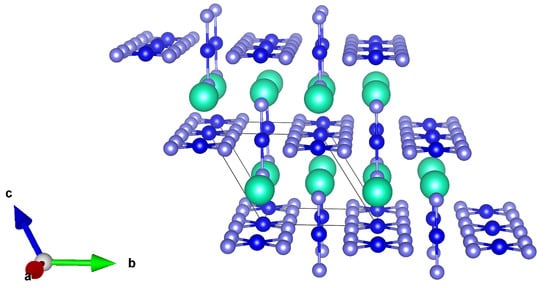
Figure 3.
Lateral view of the AuI (mauve: I atoms, blue: Au atoms, cyan: Cs atoms). (Reproduced from [53] with permission from The Royal Society of Chemistry).
At the beginning of the 90s, a group of Japanese researchers further investigated CsAuI electrical resistivity as a function of different temperatures and pressures [98]. In particular, a first-order semiconductor-to-metal transition was detected at 4.5 GPa and room temperature (RT). Still at RT, in the metallic region, another tetragonal-to-tetragonal phase transition (P = 5.5 GPa) was observed, while a metal-to-metal, tetragonal-to-cubic (P) one, has been found at higher pressure (∼6.5 GPa) and temperature (330 K) conditions. Interestingly, the oxidation state of gold was investigated with the result that, while the semiconductor (tetragonal, I, Z = 2 [99]) is characterized by Au(I) and Au(III) oxidation states, the first high pressure polymorph (still tetragonal, metallic) evolves towards a single oxidation state, Au(II), that behaves as a 2D metal (Au(II) VBM is the half-filled 5 band which spreads out in the plane). The second high-pressure polymorph is still associated with a 3D metallic behavior; i.e., an Au VBM that is Au(II) and where the degenerate 5 and 5 states are three-quarters full [98]. Very recently, this particular feature of the two-fold oxidation state in the semiconductor (room temperature and pressure) polymorph of CsAuX, has suggested that this class of compounds could be a possible candidate for Pb-free solar cells [100]. The optical gap ranges from 1.31 to 2.04 eV as a function of the halide involved, due to enhancement of the nearest-neighboring Coulomb repulsion and the JT distortion of AuX [101]. Accordingly, the iodine compound ( = 1.31 eV) seems to perfectly fulfill, in terms of optoelectronic features, what is required for a solar cell harvester. Moving from this very appealing feature, we recently investigated the electronic and optical features of this largely overlooked compound, with the main goal being to address what the role of many-body effects in the characterization of its optoelectronic properties is, and to clarify whether free-carriers or bound excitons are at the origin of the intense, largely anisotropic optical peak present in the IR/VIS region. To achieve this goal, we used a combined density functional theory (DFT) [102,103,104,105,106,107] and many-body perturbation theory (MBPT) [108,109] approach [53]. Our theoretical study shows a material characterized by a true quasi-particle direct electronic gap of 1.35 eV, a value obtained correcting by means of the GW approach the DFT-PBE bandgap of 0.63 eV. The theoretical value results in very good agreement with the experimentally reported data [101]. Analyzing the optical spectrum calculated by solving the Bethe–Salpeter Equation, we noticed that the optical transitions involve gold atoms with different oxidation states; i.e., Au(I) 5 d → Au(III) 5d orbitals, the latter mixed with I 5p and 5p (p-d hybridization). The great advantage of a ternary perovskite is the enhanced dispersion associated with the strong coupling between B-site and halide states, a feature that does not characterize the quaternary stoichiometry (see, among the others, [46] for the organic-inorganic case). This is further testified to by the calculation of the effective masses of the compound that show values comparable to the best PV performing perovskite; i.e., MAPbI [110,111]. It is, anyway, the inclusion of local-field and excitonic effects, solving the Bethe–Salpeter equation [108], that provides the most interesting features of this compound. Indeed, still showing high similarities with MAPbI, CsAuI reveals a very weakly-bound excitonic/free carrier nature of the optical excitation [53] and, additionally, the analysis of the spatial localization of the first exciton, dark and bright (reported in Figure 4), reveals a peculiar 2D behavior that reflects the optical anisotropy of the material. This finding makes the material unique: its behavior, indeed, resembles that of anatase TiO that similarly, regardless the 3D nature of the crystal, shows a bidimensional orientation of the exciton [112]. This feature could be of particular interest in low-dimensional samples where the co-existence of different facets, spatially localizing photo-generated carriers, would further boost photo-induced reactions [113]. From the device-oriented perspective, the highly anisotropic linear optical feature associated with the 2D spatial excited state distribution, can be a relevant source of optical non-linearity with a focus on optical switches in the visible region.
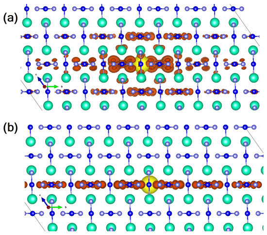
Figure 4.
Lateral view of the wavefunction square modulus of (a) the first optically inactive (dark) and (b) the first bright exciton (mauve: I atoms, blue: Au atoms, cyan: Cs atoms; the orange isosurface represents the probability of finding the electron when the hole position (yellow spot) is fixed near a given atomic site). (Reproduced from [53] with permission from The Royal Society of Chemistry).
3. Quaternary Double-Perovskites
As introduced, quaternary double-perovskites AB′(I)B″(III)X are formed when the atomic transmutation of Pb involves two different atomic species in and oxidation states. Stable double-perovskites with alternating corner shared B′X and B″X octahedra (where B′(I) = Ag, Cu; B″ = Bi, Sb, In) have been synthesized and discussed in the last five years for their possible applications in PV. They are characterized by a stable cubic structure (F) also known as elpasolite. A technological application of these crystals is in scintillators [128] since the cubic structure minimizes lattice strain during single crystal growth and reduces light scattering at grain boundaries [128,129,130]. More recently and systematically, as said, the usage of the same compounds in optoelectronics has gained particular attention. [131] Aiming at disclosing PV applicability (Table 2 collects the main available data concerning structural, electronic, optical, and PV device-oriented properties of the quaternary double-perovskites discussed in the text), Volonakis et al. [132], combining a theoretical and experimental investigation, spanned the structural and electronic properties of the whole family of halide double-perovskites A BBX with B = Sb, Bi, and B = Cu, Ag, Au. Among all the compounds, CsAgBiCl is similarly synthesized and then characterized in terms of optical absorption and photoluminescence. The calculated bandgap (PBE0 + SOC) results to be 2.7 eV (indirect) and 3.3 eV (direct), while the experimental optical gap obtained by means of UV–Vis optical absorption is about 2.2 eV [132]. (See Figure 5).
Table 2.
Main structural, electronic, optical, and PV properties of the 3D quaternary double-perovskites discussed in the text. In the first column, the species and the symmetry is reported. In the second, both theoretical (in parentheses, the level of theory) and experimental values of the lattice parameters are reported. The third column contains the bandgap, theoretical (still in parentheses, the level of calculation), and experimental (in parentheses, the experimental methodology, and absorption and photoluminescence values) values. The direct (d) and the indirect (i) nature of the gap is similarly reported. The fourth column contains the available data for the Photoconversion Efficiency ().
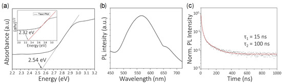
Figure 5.
Experimental synthesis and characterization of CsBiAgCl. (a) UV–Vis optical absorption spectrum of CsBiAgCl. The inset shows the Tauc plot, corresponding to an indirect allowed transition (assuming the expression: (h)1/2 = C(h – E), where is the absorption coefficient, h is the energy of the incoming photon, E is the optical band gap, and C is a constant). The straight lines are fitted to the linear regions of the absorption spectrum and Tauc plot, and the intercepts at 2.32 eV and 2.54 eV marked on the plot are calculated from the fit. (b) Steady-state photoluminescence (PL) spectrum of CsBiAgCl, deposited on glass. (c) Time-resolved photoluminescence decay of CsBiAgCl, deposited on glass. The data were fitted using a biexponential decay function. The decay lifetimes of 15 (fast) and 100 ns (slow) were estimated from the fit. (Adapted with permission from [132]. Copyright (2016) American Chemical Society.)
Several groups have then studied the double-perovskite structure, aiming at extending the applicability to optoelectronics. In one of the first attempts, Volonakis et al. [133] proposed the combination B = Ag and B = In, respectively, and reported a very interesting direct theoretical bandgap of 2.1–2.6 eV (at HSE06 level of theory) and one of 2.9–3.3 eV (at PBE0)—ranges that are function of a different structural optimization. Motivated by this finding, the authors have there approached an experimental procedure to obtain a highly stable compound whose measured UV–Vis absorbance reveals a direct gap (380 nm) of 3.3 eV (along with defect-related features at 585 nm). Zhou et al. [134] have prepared samples of the same compound by means of hydrothermal method. The obtained single-crystal of CsAgInCl is gray/transparent, confirming the gap in a range out of the visible region. Here the measured (UV–Vis) optical bandgap is 3.23 eV, while the theoretically predicted (3.33 eV) confirms that obtained by Volonakis et al. [133] Tests on the stability (powder XRD and UV–Vis diffuse reflectance spectroscopy) of the compound were performed 7, 14, and 26 days after the preparation (0 day) and revealed the good stability of CsAgInCl towards moisture, heat, and chemicals. The environmentally friendly nature of CsAgInCl together with its broad optical PL spectrum, makes this compound extremely appealing for a wide spectral range of light emission. Moving from such assumptions, Lou et al. [135] have reported CsAgInCl alloyed with Na (CsAgNaInCl) as an efficient and stable white-light emitter via self-trapped excitons due to the Jahn–Teller distortion of the AgCl octahedron in the excited state. The alloying procedure induces an excitonic absorption peak (∼365 nm), further enhancing the white emission by three orders of magnitude with respect to the pure components of the alloy. Since Na does not participate in populating the band-edges, its effect in the increase of the PLQY is mainly in the structure, with the new formed octahedron (NaCl) that tends to favor the overlap between carriers and increase the total dipole moment (the inversion-symmetry-induced parity-forbidden transition is broken). Adding Bi to the optimal alloys CsAgNaInCl has the effect of impressively enhancing the PLQY up to 86% (±5%).
The combination of B = Ag and B = Sb for the formation of CsAgSbCl [136] and CsAgSbBr [137] quaternary perovskites has been investigated, as well. For the former species, a theoretical bandgap of 2.41 eV is predicted (PAW + HSE06 level of theory), a value very close to the experimental optical gap (2.60 eV), and stability of the crystal was observed. By means of hydrothermal methods, CsAgSbBr black crystals have been synthesized being characterized by an experimental indirect optical transition at 1.64 eV (Tauc plot), while the theoretical value (HSE06 + SOC) slightly underestimates the experimental one ( 1.46 eV). Interestingly enough, the mixed-phase (due to the co-presence of secondary phases CsSbBr, CsAgBr, CsAgBr, and AgBr that brighten the color) detected in thin films shows an optical gap (UV–Vis) of ∼1.89 eV. In their work, Slavney et al. [138] show that CsAgBiBr (hereafter also CABB) is characterized by an indirect bandgap of 1.95 eV (direct bandgap at 2.21 eV, measured via a Tauc plot), a persistent room temperature fundamental photoluminescence lifetime (∼660 ns), highly suitable for PV, and additionally observed a high defect tolerance of the material which in its most stable form is characterized by a red color (as shown in Figure 6). Prolonged exposure to moisture did not induce degradation of the CsAgBiBr. even after 30 days, while eventual spots of discoloration due to the irradiation were recovered in two days by simply storing the sample in ambient light. Additionally, CABB fundamental carrier lifetime measured by means of transient absorption spectroscopy is reported to exceed 1 s [139], supporting the possible efficient usage of CABB in PV. Concurrently, McClure et al. [140] characterized CsAgBiX (X = Cl, Br) by diffuse reflectance. Their optical band gaps were 2.19 and 2.77 eV for CABB (in agreement with [138]) and the chlorine-containing perovskite, respectively. Furthermore, they concluded that CsAgBiCl shows better stability than CABB when exposed for four weeks to both light and air.
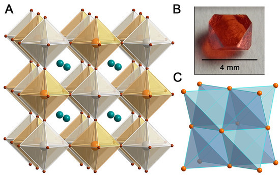
Figure 6.
(A) X-ray structure of the ordered double perovskite CsAgBiBr (1). Orange, gray, turquoise, and brown spheres represent Bi, Ag, Cs, and Br atoms, respectively. (B) Photograph of a single crystal of 1. (C) The Bi face-centered-cubic sublattice in 1, consisting of edge-sharing tetrahedra. (Reprinted with permission from [138]. Copyright (2016) American Chemical Society).
Still focusing on CABB, by means of a time-resolved microwave conductance (TRMC), Bartesaghi et al. [154] have characterized the carriers’ behavior. In detail, the shallow trap states induced by both carriers in CABB bandgap are responsible for the temperature and intensity-dependence of the lifetime of mobile charges in the bulk. The detrimental large amount of such trap states is, on the other hand, compensated by their shallow nature, and additionally, the recombination induced by such trap-states seems to take place over quite long time, revealing the potential good performances of CABB in PV. The first attempt to incorporate CsAgBiBr films on PV devices was due to the work of Greul et al. [149]: here the precursors (CsBr, AgBr and BiBr) that were dissolved in DMSO and the substrate (mesoporous (mp)-TiO) were preheated (process associated with a beneficial increase of the final device short-circuit current (J), fill factor (FF), and V) at 75 C before spin-coating the precursors on the substrate. This process was followed by a further annealing (up to 285 C) to improve the final quality of the device (see Figure 7 for the whole procedure). The hole transport layer is the commonly used 2,2,7,7-tetrakis-(N,N-di-4-methoxyphenylamino)-9,9-spirobifluorene (spiro-OMeTAD).
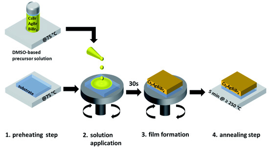
Figure 7.
Schematic of the synthesis route for CsAgBiBr thin films. The film formation (3.) occurs already while the substrate is spinning. (Reproduced from [149] with permission from The Royal Society of Chemistry).
The so-assembled (FTO)/dense TiO/mp–TiO/CsAgBiBr/spiro-OMeTAD/Au architecture thus revealed a best performance with PCE = 2.43% (J = 3.93 mA cm; V = 0.98 V, FF = 0.63) further confirming the suitability of this double–perovskites for solar devices along with an enhanced durability compared with those based on OIHPs. Back to the material investigation, in a combined theoretical and experimental analysis, Slavney et al. [155] have revealed the possibility of improving photophysical properties of CABB by alloying with thallium, nominally, Cs(AgBi)TlBr. In this way, indeed, the otherwise broad bandgap of the native compound can be tuned up to values (∼1.6 eV) competitive with those typical of OIHPs, ideal for a single-junction photovoltaic absorber. Replacing Ag with Tl at x = 0.06 is reported to swap the nature of the bandgap of the final material from indirect to direct, with several interesting implications for device applications. Along the same lines, the Mitzi and the Yan groups [156] proposed band gap engineering through Bi substitution with Sb or In: CsAg(BiM)Br. They synthesized three In substituted structures with 25%, 50% and 75% and two Sb with 12.5% and 37.5% and found that indium increases the band gap while antimony decreases it (with respect to CABB), offering a 0.41 eV band gap modulation window. Notably, CsAg(BiIn)Br intensified the PL intensity in comparison with the unsubstituted perovskite; all other alloys decreased it. High pressure has also been used to engineer the band gap of CABB [157]. It changes from cubic (Fm-3m) to tetragonal (I4/m) phase at 4.5 GPa, preserving the band gap unchanged at ∼2.19 eV. Increasing pressure up to 6.5 GPa results in a small band gap broadening (2.3 eV), while further increments (∼15 GPa) narrow the band gap down to 1.7 eV. The authors speculate that structural amorphization is responsible for such an impressive effect. Moreover, it is reported that releasing the pressure back to ambient conditions resulted in a 2.0 eV band gap. Nanocrystallization is also possible for CsAgBiBr, even if the quaternary nature of such compounds clearly requires more care in such a size-reduction process in order to keep the correct stoichiometry of the material itself. By means of hot-injection process [144], colloidal nanocrystals of CsAgBiX (X = Cl, Br) elpasolite are synthesized and characterized. For 8–9 nm samples the absorption spectrum shows a feature at 3.39 eV for X = Cl and at 2.87 eV for X = Br. At 20 K, a single emission PL peak is observed at 1.68 eV (single broad emission band) for X = Cl while for X = Br two emission bands, around 1.75 eV, and a more intense, narrower feature centered at 1.97 eV, are observed. This latter red-shifts to 1.92 eV at room temperature. The authors here ascribe the origin of the low energy peak in PL to a common cause in both halides, i.e., a surface-related defect, while for the X = Br high energy feature they do not report any tentative explanation (see Figure 8). The same authors report, by means of an anion-exchange process, the possible formation of the previously not reported CsAgBiI for which no visible room temperature PL is observed (at 20 K a broad, low-energy emission is observed). The (indirect) bandgaps for the three halides are here reported to be 2.89, 2.33, and 1.75 eV for X = Cl, Br, and I, respectively.
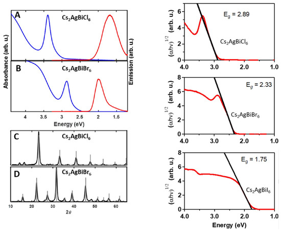
Figure 8.
(Left) (A,B) Absorption (blue) and emission (red) spectra of 8 nm CsAgBiCl (A) and CsAgBiBr (B) nanocrystals. Absorption spectra were collected from hexane solutions at room temperature and emission spectra were collected on thin films at 20 K using 405 nm (for CsAgBiBr) or 365 nm (for CsAgBiCl) excitation. (Right): Tauc analysis of indirect bandgaps in CsAgBiX. (X = Cl, Br, I). (Adapted with permission from [144]. Copyright (2018) American Chemical Society).
Yang et al. [158] have synthesized and characterized the three halide CsAgBiX (X = Cl, Br, I) NCs; they found appealing features also at 0D. It is worth mentioning here that surface defects play the main role in determining the optoelectronic properties of such NCs. A sub-bandgap trapping is reported, an effect that, anyway, is mitigated by the usage of capping agents (Oleic Acid). In the case of X = Br, transient absorption measurements reveal fast hot-carrier relaxation (<1 ps) process competitive in time scale with the mentioned trapping processes.
Still on the NC realm, Bekenstein, et al. [159] studied the optical properties of CsAgBiX (X = Cl, Br). The authors synthesized 8–15 nm NCs by means of two different paths. The first is a modified version of that used by Protesescu et al. [160] for CsPbX NC synthesis and consists of an injection of Cs-oleate in a solution of precursors (AgBr and BiBr) in octadecene with oleylamine and oleic acid at a high temperature. The second follows that of Xu et al. [161] and consists of a lower temperature injection of halide precursor into a solution of metal acetates. NCs obtained show a similar XRD pattern of the corresponding 3D phases. Concerning the optical features of the two halides, a sharp peak (1 eV higher in energy than the band edge, ascribed to a Bi 6s–6p transition) at 430 nm (X = Br) and 365 nm X = Cl) arises in absorption spectra of such NCs. More exotic seems to be the CsNaBiX class of compounds: while only the X = Cl [162,163] was initially investigated, more recently the X = Br and X = I compounds have been at first theoretically predicted [164]. and then in a couple of very recent papers [165,166], high quality CsNaBiI films have been synthesized and applied as solar harvesters. The oost treatment procedure (isopropyl alcohol soaking and DMF annealing) has led to a ten-fold improvement of the solar device PCE (0.021% to 0.21%) with no loss even after 100 days in ambient conditions. Among all the quaternary double-perovskites, probably the most investigated and with enhanced applicability in optoelectronics is represented by the indirect bandgap CsAgBiBr perovskite. In our research [54], we have tried to focus on the debated, yet undisclosed origin of the Stokes shift in PL, whose peak is reported fairly below 2.0 eV, and the UV–Vis spectra which has a peak above 2.0 eV [138,167,168]. In order to do it, we have compared the structural, electronic, and optical features of CABB with that of other two double-perovskites but with ternary stoichiometry; i.e., CsInX (or CsIn(I)In(III)X) with X=F, Br [169]. Our quasiparticle (QP) electronic band structures obtained within the GW perturbative approach confirmed the indirect nature of the bandgap of CABB and other compounds (see Figure 9). Additionally the values obtained are in line with previously calculated ones, but a larger opening of the gap was observed due to the self-consistent cycles (eigenvalues only evGW) in the GW calculations.
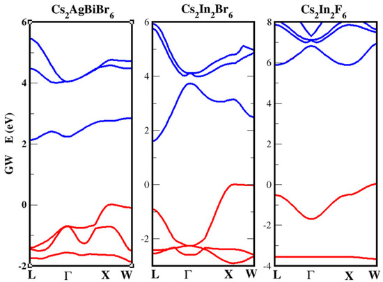
Figure 9.
Quasiparticle (QP) electronic band structures obtained within the GW perturbative approach; red (blue) indicates occupied (unoccupied) bands. The top of the valence band has been shifted to zero energy for all cases. (Reprinted with permission from [54]. Copyright (2020) American Chemical Society).
As a general behavior, we observe that the Density of States (DOS) of the three materials shows sharper and narrow peaks near the VBM with respect to the CBM. Accordingly, we can state that the carrier non-radiative lifetime should be shorter for holes with respect to electrons: it is well known indeed that a smooth (narrow) DOS corresponds to a reduced (larger) number of carrier relaxation paths that lead to longer (shorter) carrier lifetimes [12,170,171,172]. We then calculated the optical spectra [108] of the three materials by solving the Bethe–Salpeter equation within the Tamm-Dancoff approximation (see Figure 10) [173,174]. With particular attention to CABB compound, we observe a peak at ∼2.3 eV. We focus then on the energy loss function calculated at the q vectors of interest (q = L–X, –X, red solid and dashed curves in Figure 10) and including the e–h interaction. This calculation can provide clear evidence of the presence of indirect bound excitons, allowing one to verify if their energy is in the same range of the observed PL emission. Indeed, assuming as the most probable process the one involving a single LO phonon and if this mode has a very small energy (see [54] for further details), the PL spectrum should have the onset at the same energy of the lowest indirect excitons. Notably, the EELS spectra (red curves) show peaks below 2 eV, in the same energetic region of the observed PL (shaded yellow rectangle). This provides a strong indication of the fact that the PL is due to phonon-assisted radiative recombination of indirect bound excitons with q = L–X, –X and energies 1.8, and 1.9 eV, respectively. From our analysis, we can conclude that the large measured Stokes shift is compatible with the energy difference between the direct and the indirect excitonic interband transitions.
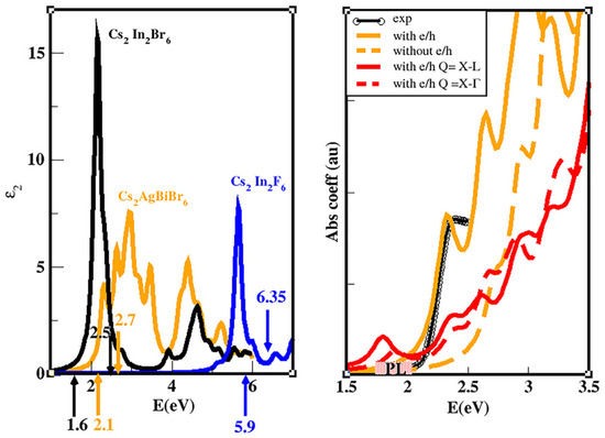
Figure 10.
(Left) Imaginary part of the dielectric function for the three double perovskites, obtained taking into account the QP corrections calculated at the GW level of approximation and also including the excitonic and local-field effects through the solution of the BSE. The up-oriented (down) arrows (and relative numbers) indicate the energetic positions of the indirect (direct) minimum QP gap. (Right) Theoretical absorption coefficient with (orange solid curve) and without (orange dashed curve) the local field and excitonic effects, compared with the experimental curve (black curve) from [138]. The red (dashed and solid) curves are the EELS spectra calculated with e–h effects included for finite transferred momentum Q corresponding to the lowest indirect transition L–X and –X, respectively. The energetic region where the PL is observed is indicated schematically by the shaded yellow area. (Reprinted with permission from [54]. Copyright (2020) American Chemical Society).
It is worth mentioning that during the drafting of the present review, Dey al. by means of an experimental analysis (time-resolved PL and differential transmission spectroscopy) have ascribed the high energy (2.88 eV) emission to the radiative recombination of direct bound excitons characterized by giant oscillator strength, and that should be the origin of both the absorption peak at the optical bandgap and of the luminescence at the direct bandgap transition [175].
It is worth stressing here that according to their large absorption coefficients and gap in the VIS region, both CsAgBiBr and CsInBr are clearly materials of interest for possible PV applications. The spectroscopic limited maximum efficiency (SLME) [176,177] whose calculation requires several variables, such as the standard solar spectrum, the absorption coefficient of the material, and also the values of the direct/indirect electronic gaps (the latter we have calculated at the quasi-particle level of theory, within the method), represents a theoretical tool to compare with the experimental PCE of a solar harvester. We have calculated it for CABB, for the other three ternary double-perovskites, and as reference for MAPbI. Interestingly, our results show a very good agreement between PCE (25.2% [2] and SLME (26%) for MAPbI, testifying to the fact that the limit has been almost achieved. At the same time, SLME predicts large room to improve performances in solar devices for CABB whose experimental PCE is 3% [148,149,178]. Additionally CsInBr (SLME = 11.5%) shows interesting potentiality (to the best of our knowledge no PCE data for CsInBr-based PSCs are available in literature). Noticeably, the previously discussed CsAuI is characterized by a SLME value of 30% further witnessing how much this material has been (and is) overlooked for any potential PV and optolelectronic applications.
Hybrid organic-inorganic perovskites have been shown to be the PV big thing of the decade. Regardless their dimensionality and applications [10,53,179,180,181], indeed, OIHPs have revealed impressive performances in optoelectronics. As the Shockley–Queisser limit has been approached for PV-oriented applications, the need for better performing, beyond single-junction devices is becoming mandatory. Very recent works [182,183,184,185,186] have shown the great potentiality of OIHPs in tandem devices, both two- and four-terminal architectures. Initial tandem cells characterized by PCE = 13.7% [182] have been improved and thanks to the usage of silicon pyramidal texture PCEs of 25.2% have been obtained [183] and passed (a 27.3% PCE has been announced for Si/OIHPs device). Extending the solutions to the pitfalls of single-junction OIHPs-based systems to tandem cells, we believe the replacement of OIHPs with fully inorganic perovskites, both ternary and quaternary, is a viable and powerful route to enhance the stability of such multi-junction devices. The indirect bandgap at ∼1.95 eV for double-perovskites (CsAgBiBr) makes them materials suitable for tandem devices [138]. Not only will any other application based on the Si/(halide perovskite) interface [187,188],photodetectors [189] be beneficially impacted by the replacement of OIHPs with inorganic perovskites in terms of device stability and durability [190], the real Achilles heel for the OIHPs device mass production, but light-emitting applications [191] will too. Finally, it is worth stressing the fact that recent years have faced a huge increase of available computational power. Accordingly, the branch of the high-throughput screening has become a real must for the search of novel materials with properties focused on optoelectronics [192]. Additionally, halide perovskites, both hybrid and purely inorganic [193,194,195,196,197,198], have been recently investigated with extremely encouraging results [199,200] and in this sense, as theoreticians, we expect a further boost of the appealing investigations of this kind able to reduce issues (costs and pollution, among the others) associated with a massive experimental activity.
4. Conclusions
In conclusion, in view of the detrimental structural shortcomings that characterized the well-known and investigated class of hybrid organic-inorganic halide perovskites, i.e., the presence of toxic lead and that of a hydrophilic moiety (methylammonium, MA=CHNH), we have here revised most of the literature and results concerning Pb-free fully-inorganic halide perovskites. In particular, the two classes of ternary and quaternary stoichiometric double-perovskites have been discussed also in view of the results our group has obtained in recent years. Considering the enhanced intrinsic stability provided by the metallic cation in the A-site of the perovskite network, experimental evidence supported by theoretical data encourage the continuation of the theoretical and experimental investigation of other ternary and quaternary double-perovskites.
Author Contributions
Conceptualization, G.G. and M.P.; writing–original draft preparation, G.G.; writing–review and editing, M.P., D.V., E.B., K.Y. All authors have read and agreed to the published version of the manuscript.
Funding
This work was partially supported by the MaX—MAterials design at the eXascale—Centre of Excellence, funded by the European Union program H2020-INFRAEDI-2018-1 (grant number 824143). The authors acknowledge PRACE for awarding them access to the Marconi system based in Italy at CINECA and the Italian ISCRA program.
Conflicts of Interest
The authors declare no conflict of interest.
References
- Kojima, A.; Teshima, K.; Shirai, Y.; Miyasaka, T. Organometal Halide Perovskites as Visible–Light Sensitizers for Photovoltaic Cells. J. Am. Chem. Soc. 2009, 131, 6050–6051. [Google Scholar] [CrossRef] [PubMed]
- Best Research-Cell Efficiency Chart. Available online: https://www.nrel.gov/pv/assets/pdfs/best-research-cell-efficiencies.20190802.pdf (accessed on 10 June 2020).
- Baikie, T.; Fang, Y.; Kadro, J.M.; Schreyer, M.; Wei, F.; Mhaisalkar, S.G.; Grätzel, M.; White, T.J. Synthesis and crystal chemistry of the hybrid perovskite (CH3NH3)PbI3 for solid-state sensitised solar cell applications. J. Mater. Chem. A 2013, 1, 5628–5641. [Google Scholar] [CrossRef]
- Xing, G.; Mathews, N.; Sun, S.; Lim, S.S.; Lam, Y.M.; Grätzel, M.; Mhaisalkar, S.; Sum, T.C. Long-range balanced electron-and hole-transport lengths in organic-inorganic CH3NH3PbI3. Science 2013, 342, 344–347. [Google Scholar] [CrossRef] [PubMed]
- Stranks, S.D.; Eperon, G.E.; Grancini, G.; Menelaou, C.; Alcocer, M.J.; Leijtens, T.; Herz, L.M.; Petrozza, A.; Snaith, H.J. Electron-hole diffusion lengths exceeding 1 micrometer in an organometal trihalide perovskite absorber. Science 2013, 342, 341–344. [Google Scholar] [CrossRef] [PubMed]
- Heo, J.H.; Im, S.H.; Noh, J.H.; Mandal, T.N.; Lim, C.S.; Chang, J.A.; Lee, Y.H.; Kim, H.j.; Sarkar, A.; Nazeeruddin, M.K.; et al. Efficient inorganic–organic hybrid heterojunction solar cells containing perovskite compound and polymeric hole conductors. Nat. Photonics 2013, 7, 486. [Google Scholar] [CrossRef]
- Etgar, L.; Gao, P.; Xue, Z.; Peng, Q.; Chandiran, A.K.; Liu, B.; Nazeeruddin, M.K.; Grätzel, M. Mesoscopic CH3NH3PbI3/TiO2 heterojunction solar cells. J. Am. Chem. Soc. 2012, 134, 17396–17399. [Google Scholar] [CrossRef]
- Laban, W.A.; Etgar, L. Depleted hole conductor-free lead halide iodide heterojunction solar cells. Energy Environ. Sci. 2013, 6, 3249–3253. [Google Scholar] [CrossRef]
- Lee, M.M.; Teuscher, J.; Miyasaka, T.; Murakami, T.N.; Snaith, H.J. Efficient hybrid solar cells based on meso-superstructured organometal halide perovskites. Science 2012, 338, 643–647. [Google Scholar] [CrossRef]
- Giorgi, G.; Fujisawa, J.I.; Segawa, H.; Yamashita, K. Small photocarrier effective masses featuring ambipolar transport in methylammonium lead iodide perovskite: A density functional analysis. J. Phys. Chem. Lett. 2013, 4, 4213–4216. [Google Scholar] [CrossRef]
- Giorgi, G.; Yamashita, K. Organic–inorganic halide perovskites: An ambipolar class of materials with enhanced photovoltaic performances. J. Mater. Chem. A 2015, 3, 8981–8991. [Google Scholar] [CrossRef]
- Kawai, H.; Giorgi, G.; Marini, A.; Yamashita, K. The mechanism of slow hot-hole cooling in lead-iodide perovskite: First-principles calculation on carrier lifetime from electron–phonon interaction. Nano Lett. 2015, 15, 3103–3108. [Google Scholar] [CrossRef] [PubMed]
- Mosconi, E.; Amat, A.; Nazeeruddin, M.K.; Grätzel, M.; De Angelis, F. First-principles modeling of mixed halide organometal perovskites for photovoltaic applications. J. Phys. Chem. C 2013, 117, 13902–13913. [Google Scholar] [CrossRef]
- Even, J.; Pedesseau, L.; Jancu, J.M.; Katan, C. Importance of spin–orbit coupling in hybrid organic/inorganic perovskites for photovoltaic applications. J. Phys. Chem. Lett. 2013, 4, 2999–3005. [Google Scholar] [CrossRef]
- Snaith, H.J.; Abate, A.; Ball, J.M.; Eperon, G.E.; Leijtens, T.; Noel, N.K.; Stranks, S.D.; Wang, J.T.W.; Wojciechowski, K.; Zhang, W. Anomalous hysteresis in perovskite solar cells. J. Phys. Chem. Lett. 2014, 5, 1511–1515. [Google Scholar] [CrossRef] [PubMed]
- Giorgi, G.; Yamashita, K. Zero-dipole molecular organic cations in mixed organic–inorganic halide perovskites: Possible chemical solution for the reported anomalous hysteresis in the current–voltage curve measurements. Nanotechnology 2015, 26, 442001. [Google Scholar] [CrossRef] [PubMed]
- Giorgi, G.; Fujisawa, J.I.; Segawa, H.; Yamashita, K. Organic–inorganic hybrid lead iodide perovskite featuring zero dipole moment guanidinium cations: A theoretical analysis. J. Phys. Chem. C 2015, 119, 4694–4701. [Google Scholar] [CrossRef]
- Stroppa, A.; Quarti, C.; De Angelis, F.; Picozzi, S. Ferroelectric polarization of CH3NH3PbI3: A detailed study based on density functional theory and symmetry mode analysis. J. Phys. Chem. Lett. 2015, 6, 2223–2231. [Google Scholar] [CrossRef]
- Zhang, Y.; Liu, M.; Eperon, G.E.; Leijtens, T.C.; McMeekin, D.; Saliba, M.; Zhang, W.; de Bastiani, M.; Petrozza, A.; Herz, L.M.; et al. Charge selective contacts, mobile ions and anomalous hysteresis in organic–inorganic perovskite solar cells. Mater. Horizons 2015, 2, 315–322. [Google Scholar] [CrossRef]
- Tress, W.; Marinova, N.; Moehl, T.; Zakeeruddin, S.M.; Nazeeruddin, M.K.; Grätzel, M. Understanding the rate-dependent J–V hysteresis, slow time component, and aging in CH3NH3PbI3 perovskite solar cells: The role of a compensated electric field. Energy Environ. Sci. 2015, 8, 995–1004. [Google Scholar] [CrossRef]
- Li, C.; Tscheuschner, S.; Paulus, F.; Hopkinson, P.E.; Kießling, J.; Köhler, A.; Vaynzof, Y.; Huettner, S. Iodine migration and its effect on hysteresis in perovskite solar cells. Adv. Mater. 2016, 28, 2446–2454. [Google Scholar] [CrossRef] [PubMed]
- Calado, P.; Telford, A.M.; Bryant, D.; Li, X.; Nelson, J.; O’Regan, B.C.; Barnes, P.R. Evidence for ion migration in hybrid perovskite solar cells with minimal hysteresis. Nat. Commun. 2016, 7, 13831. [Google Scholar] [CrossRef] [PubMed]
- Kieslich, G.; Sun, S.; Cheetham, A.K. Solid-state principles applied to organic–inorganic perovskites: New tricks for an old dog. Chem. Sci. 2014, 5, 4712–4715. [Google Scholar] [CrossRef]
- De Marco, N.; Zhou, H.; Chen, Q.; Sun, P.; Liu, Z.; Meng, L.; Yao, E.P.; Liu, Y.; Schiffer, A.; Yang, Y. Guanidinium: A route to enhanced carrier lifetime and open-circuit voltage in hybrid perovskite solar cells. Nano Lett. 2016, 16, 1009–1016. [Google Scholar] [CrossRef] [PubMed]
- Pham, N.D.; Zhang, C.; Tiong, V.T.; Zhang, S.; Will, G.; Bou, A.; Bisquert, J.; Shaw, P.E.; Du, A.; Wilson, G.J.; et al. Tailoring crystal structure of FA0.83Cs0.17PbI3 perovskite Through guanidinium doping for Enhanced performance and Tunable hysteresis of planar perovskite solar cells. Adv. Funct. Mater. 2019, 29, 1806479. [Google Scholar] [CrossRef]
- Cheng, N.; Li, W.; Zhang, M.; Wu, H.; Sun, S.; Zhao, Z.; Xiao, Z.; Sun, Z.; Zi, W.; Fang, L. Enhance the performance and stability of methylammonium lead iodide perovskite solar cells with guanidinium thiocyanate additive. Curr. Appl. Phys. 2019, 19, 25–30. [Google Scholar] [CrossRef]
- Gong, J.; Guo, P.; Benjamin, S.E.; Van Patten, P.G.; Schaller, R.D.; Xu, T. Cation engineering on lead iodide perovskites for stable and high-performance photovoltaic applications. J. Energy Chem. 2018, 27, 1017–1039. [Google Scholar] [CrossRef]
- Jodlowski, A.D.; Roldán-Carmona, C.; Grancini, G.; Salado, M.; Ralaiarisoa, M.; Ahmad, S.; Koch, N.; Camacho, L.; De Miguel, G.; Nazeeruddin, M.K. Large guanidinium cation mixed with methylammonium in lead iodide perovskites for 19% efficient solar cells. Nat. Energy 2017, 2, 972–979. [Google Scholar] [CrossRef]
- Kubicki, D.J.; Prochowicz, D.; Hofstetter, A.; Saski, M.; Yadav, P.; Bi, D.; Pellet, N.; Lewinski, J.; Zakeeruddin, S.M.; Grätzel, M.; et al. Formation of Stable mixed guanidinium–methylammonium phases with exceptionally long carrier lifetimes for high-efficiency lead iodide-based perovskite photovoltaics. J. Am. Chem. Soc. 2018, 140, 3345–3351. [Google Scholar] [CrossRef]
- Niu, G.; Guo, X.; Wang, L. Review of recent progress in chemical stability of perovskite solar cells. J. Mater. Chem. A 2015, 3, 8970–8980. [Google Scholar] [CrossRef]
- Han, Y.; Meyer, S.; Dkhissi, Y.; Weber, K.; Pringle, J.M.; Bach, U.; Spiccia, L.; Cheng, Y.B. Degradation observations of encapsulated planar CH3NH3PbI3 perovskite solar cells at high temperatures and humidity. J. Mater. Chem. A 2015, 3, 8139–8147. [Google Scholar] [CrossRef]
- Mosconi, E.; Azpiroz, J.M.; De Angelis, F. Ab initio molecular dynamics simulations of methylammonium lead iodide perovskite degradation by water. Chem. Mater. 2015, 27, 4885–4892. [Google Scholar] [CrossRef]
- Stoumpos, C.C.; Cao, D.H.; Clark, D.J.; Young, J.; Rondinelli, J.M.; Jang, J.I.; Hupp, J.T.; Kanatzidis, M.G. Ruddlesden–Popper hybrid lead iodide perovskite 2D homologous semiconductors. Chem. Mater. 2016, 28, 2852–2867. [Google Scholar] [CrossRef]
- Tsai, H.; Nie, W.; Blancon, J.C.; Stoumpos, C.C.; Asadpour, R.; Harutyunyan, B.; Neukirch, A.J.; Verduzco, R.; Crochet, J.J.; Tretiak, S.; et al. High-efficiency two-dimensional Ruddlesden–Popper perovskite solar cells. Nature 2016, 536, 312–316. [Google Scholar] [CrossRef] [PubMed]
- Mao, L.; Ke, W.; Pedesseau, L.; Wu, Y.; Katan, C.; Even, J.; Wasielewski, M.R.; Stoumpos, C.C.; Kanatzidis, M.G. Hybrid Dion–Jacobson 2D lead iodide perovskites. J. Am. Chem. Soc. 2018, 140, 3775–3783. [Google Scholar] [CrossRef] [PubMed]
- Mitzi, D.B. Synthesis, structure, and properties of organic-inorganic perovskites and related materials. Prog. Inorg. Chem. 1999, 48, 1–121. [Google Scholar]
- Mitzi, D.B.; Feild, C.; Harrison, W.; Guloy, A. Conducting tin halides with a layered organic-based perovskite structure. Nature 1994, 369, 467–469. [Google Scholar] [CrossRef]
- Mitzi, D.B. Synthesis, crystal structure, and optical and thermal properties of (C4H9NH3) 2MI4 (M= Ge, Sn, Pb). Chem. Mater. 1996, 8, 791–800. [Google Scholar] [CrossRef]
- Smith, I.C.; Hoke, E.T.; Solis-Ibarra, D.; McGehee, M.D.; Karunadasa, H.I. A layered hybrid perovskite solar-cell absorber with enhanced moisture stability. Angew. Chem. Int. Ed. 2014, 53, 11232–11235. [Google Scholar] [CrossRef] [PubMed]
- Cao, D.H.; Stoumpos, C.C.; Farha, O.K.; Hupp, J.T.; Kanatzidis, M.G. 2D homologous perovskites as light-absorbing materials for solar cell applications. J. Am. Chem. Soc. 2015, 137, 7843–7850. [Google Scholar] [CrossRef]
- Giorgi, G.; Yamashita, K.; Palummo, M. Nature of the Electronic and Optical Excitations of Ruddlesden–Popper Hybrid Organic–Inorganic Perovskites: The Role of the Many-Body Interactions. J. Phys. Chem. Lett. 2018, 9, 5891–5896. [Google Scholar] [CrossRef]
- Stoumpos, C.C.; Frazer, L.; Clark, D.J.; Kim, Y.S.; Rhim, S.H.; Freeman, A.J.; Ketterson, J.B.; Jang, J.I.; Kanatzidis, M.G. Hybrid germanium iodide perovskite semiconductors: Active lone pairs, structural distortions, direct and indirect energy gaps, and strong nonlinear optical properties. J. Am. Chem. Soc. 2015, 137, 6804–6819. [Google Scholar] [CrossRef] [PubMed]
- Sun, P.P.; Li, Q.S.; Yang, L.N.; Li, Z.S. Theoretical insights into a potential lead-free hybrid perovskite: Substituting Pb2+ with Ge2+. Nanoscale 2016, 8, 1503–1512. [Google Scholar] [CrossRef] [PubMed]
- Hao, F.; Stoumpos, C.C.; Guo, P.; Zhou, N.; Marks, T.J.; Chang, R.P.; Kanatzidis, M.G. Solvent-mediated crystallization of CH3NH3SnI3 films for heterojunction depleted perovskite solar cells. J. Am. Chem. Soc. 2015, 137, 11445–11452. [Google Scholar] [CrossRef] [PubMed]
- Ogomi, Y.; Morita, A.; Tsukamoto, S.; Saitho, T.; Fujikawa, N.; Shen, Q.; Toyoda, T.; Yoshino, K.; Pandey, S.S.; Ma, T.; et al. CH3NH3SnxPb(1−x)I3 Perovskite solar cells covering up to 1060 nm. J. Phys. Chem. Lett. 2014, 5, 1004–1011. [Google Scholar] [CrossRef] [PubMed]
- Giorgi, G.; Yamashita, K. Alternative, lead-free, hybrid organic–inorganic perovskites for solar applications: A DFT analysis. Chem. Lett. 2015, 44, 826–828. [Google Scholar] [CrossRef]
- Weber, D. CH3NH3PbX3, ein Pb (II)-system mit kubischer perowskitstruktur/ CH3NH3PbX3, a Pb (II)-system with cubic perovskite structure. Z. Für Naturforschung B 1978, 33, 1443–1445. [Google Scholar] [CrossRef]
- Weber, D. CH3NH3SnBrxI3−x (x = 0–3), ein Sn (II)-System mit kubischer Perowskitstruktur/ CH3NH3SnBrxI3−x (x = 0–3), a Sn (II)-system with cubic perovskite structure. Z. Für Naturforschung B 1978, 33, 862–865. [Google Scholar] [CrossRef]
- Stoumpos, C.C.; Malliakas, C.D.; Kanatzidis, M.G. Semiconducting tin and lead iodide perovskites with organic cations: Phase transitions, high mobilities, and near-infrared photoluminescent properties. Inorg. Chem. 2013, 52, 9019–9038. [Google Scholar] [CrossRef]
- Chen, S.; Gong, X.; Walsh, A.; Wei, S.H. Crystal and electronic band structure of Cu2ZnSnX4 (X = S and Se) photovoltaic absorbers: First-principles insights. Appl. Phys. Lett. 2009, 94, 041903. [Google Scholar] [CrossRef]
- Chen, S.; Gong, X.; Walsh, A.; Wei, S.H. Electronic structure and stability of quaternary chalcogenide semiconductors derived from cation cross-substitution of II-VI and I-III-VI2 compounds. Phys. Rev. B 2009, 79, 165211. [Google Scholar] [CrossRef]
- Zhao, X.G.; Yang, J.H.; Fu, Y.; Yang, D.; Xu, Q.; Yu, L.; Wei, S.H.; Zhang, L. Design of lead-free inorganic halide perovskites for solar cells via cation-transmutation. J. Am. Chem. Soc. 2017, 139, 2630–2638. [Google Scholar] [CrossRef] [PubMed]
- Giorgi, G.; Yamashita, K.; Palummo, M. Two-dimensional optical excitations in the mixed-valence Cs2Au2I6 fully inorganic double perovskite. J. Mater. Chem. C 2018, 6, 10197–10201. [Google Scholar] [CrossRef]
- Palummo, M.; Berrios, E.; Varsano, D.; Giorgi, G. Optical Excitations of Lead-free Double Perovskites by Ab-initio Excited-State Methods. ACS Energy Lett. 2020, 5, 457–463. [Google Scholar] [CrossRef]
- Kieslich, G.; Sun, S.; Cheetham, A.K. An extended tolerance factor approach for organic–inorganic perovskites. Chem. Sci. 2015, 6, 3430–3433. [Google Scholar] [CrossRef] [PubMed]
- Goldschmidt, V.M. Die gesetze der krystallochemie. Naturwissenschaften 1926, 14, 477–485. [Google Scholar] [CrossRef]
- Kubo, A.; Giorgi, G.; Yamashita, K. MgTaO2N photocatalysts: Perovskite versus ilmenite structure. A theoretical investigation. J. Phys. Chem. C 2017, 121, 27813–27821. [Google Scholar] [CrossRef]
- Huang, L.Y.; Lambrecht, W.R. Electronic band structure, phonons, and exciton binding energies of halide perovskites CsSnCl3, CsSnBr3, and CsSnI3. Phys. Rev. B 2013, 88, 165203. [Google Scholar] [CrossRef]
- Huang, L.Y.; Lambrecht, W.R. Vibrational spectra and nonlinear optical coefficients of rhombohedral CsGeX3 halide compounds with X= I, Br, Cl. Phys. Rev. B 2016, 94, 115202. [Google Scholar] [CrossRef]
- Chung, I.; Song, J.H.; Im, J.; Androulakis, J.; Malliakas, C.D.; Li, H.; Freeman, A.J.; Kenney, J.T.; Kanatzidis, M.G. CsSnI3: Semiconductor or metal? High electrical conductivity and strong near-infrared photoluminescence from a single material. High hole mobility and phase-transitions. J. Am. Chem. Soc. 2012, 134, 8579–8587. [Google Scholar] [CrossRef]
- Lee, B.; He, J.; Chang, R.P.; Kanatzidis, M.G. All-solid-state dye-sensitized solar cells with high efficiency. Nature 2012, 485, 486–489. [Google Scholar]
- Qiu, X.; Cao, B.; Yuan, S.; Chen, X.; Qiu, Z.; Jiang, Y.; Ye, Q.; Wang, H.; Zeng, H.; Liu, J.; et al. From unstable CsSnI3 to air-stable Cs2SnI6: A lead-free perovskite solar cell light absorber with bandgap of 1.48 eV and high absorption coefficient. Sol. Energy Mater. Sol. Cells 2017, 159, 227–234. [Google Scholar] [CrossRef]
- Xu, L.; Yuan, S.; Zeng, H.; Song, J. A comprehensive review of doping in perovskite nanocrystals/quantum dots: Evolution of structure, electronics, optics and light-emitting diodes. Mater. Today Nano 2019, 6, 100036. [Google Scholar] [CrossRef]
- Liang, J.; Chen, D.; Yao, X.; Zhang, K.; Qu, F.; Qin, L.; Huang, Y.; Li, J. Recent Progress and Development in Inorganic Halide Perovskite Quantum Dots for Photoelectrochemical Applications. Small 2020, 16, 1903398. [Google Scholar] [CrossRef] [PubMed]
- Wang, Y.; Tu, J.; Li, T.; Tao, C.; Deng, X.; Li, Z. Convenient preparation of CsSnI3 quantum dots, excellent stability, and the highest performance of lead-free inorganic perovskite solar cells so far. J. Mater. Chem. A 2019, 7, 7683–7690. [Google Scholar] [CrossRef]
- Even, J.; Pedesseau, L.; Jancu, J.M.; Katan, C. DFT and k· p modelling of the phase transitions of lead and tin halide perovskites for photovoltaic cells. Phys. Status Solidi (RRL) Res. Lett. 2014, 8, 31–35. [Google Scholar] [CrossRef]
- Mori, M.; Saito, H. An X-ray study of successive phase transitions in CsSnBr3. J. Phys. C: Solid State Phys. 1986, 19, 2391–2401. [Google Scholar] [CrossRef]
- Kuok, M.H.; Saw, E.L.; Yap, C.T. A Mössbauer Study of the Phase Transitions in CsSnBr3. Phys. Status Solidi (a) 1992, 132, K89–K92. [Google Scholar] [CrossRef]
- Fabini, D.H.; Laurita, G.; Bechtel, J.S.; Stoumpos, C.C.; Evans, H.A.; Kontos, A.G.; Raptis, Y.S.; Falaras, P.; Van der Ven, A.; Kanatzidis, M.G.; et al. Dynamic Stereochemical Activity of the Sn2+ Lone Pair in Perovskite CsSnBr3. J. Am. Chem. Soc. 2016, 138, 11820–11832. [Google Scholar] [CrossRef]
- Sabba, D.; Mulmudi, H.K.; Prabhakar, R.R.; Krishnamoorthy, T.; Baikie, T.; Boix, P.P.; Mhaisalkar, S.; Mathews, N. Impact of Anionic Br– Substitution on Open Circuit Voltage in Lead Free Perovskite (CsSnI3−xBrx) Solar Cells. J. Phys. Chem. C 2015, 119, 1763–1767. [Google Scholar] [CrossRef]
- Krishnamoorthy, T.; Ding, H.; Yan, C.; Leong, W.L.; Baikie, T.; Zhang, Z.; Sherburne, M.; Li, S.; Asta, M.; Mathews, N.; et al. Lead-free germanium iodide perovskite materials for photovoltaic applications. J. Mater. Chem. A 2015, 3, 23829–23832. [Google Scholar] [CrossRef]
- Ming, W.; Shi, H.; Du, M.H. Large dielectric constant, high acceptor density, and deep electron traps in perovskite solar cell material CsGeI3. J. Mater. Chem. A 2016, 4, 13852–13858. [Google Scholar] [CrossRef]
- Roknuzzaman, M.; Ostrikov, K.K.; Wang, H.; Du, A.; Tesfamichael, T. Towards lead-free perovskite photovoltaics and optoelectronics by ab-initio simulations. Sci. Rep. 2017, 7, 14025. [Google Scholar] [CrossRef] [PubMed]
- Nakajima, T.; Sawada, K. Discovery of Pb-free perovskite solar cells via high-throughput simulation on the K computer. J. Phys. Chem. Lett. 2017, 8, 4826–4831. [Google Scholar] [CrossRef] [PubMed]
- Moussa, J.E.; Schultz, P.A.; Chelikowsky, J.R. Analysis of the Heyd-Scuseria-Ernzerhof density functional parameter space. J. Chem. Phys. 2012, 136, 204117. [Google Scholar] [CrossRef] [PubMed]
- Shockley, W.; Queisser, H.J. Detailed balance limit of efficiency of p-n junction solar cells. J. Appl. Phys. 1961, 32, 510–519. [Google Scholar] [CrossRef]
- Shannon, R.D. Revised effective ionic radii and systematic studies of interatomic distances in halides and chalcogenides. Acta Crystallogr. Sect. A Cryst. Physics Diffraction Theor. Gen. Crystallogr. 1976, 32, 751–767. [Google Scholar] [CrossRef]
- Ge, S.; Guan, X.; Wang, Y.; Lin, C.H.; Cui, Y.; Huang, Y.; Zhang, X.; Zhang, R.; Yang, X.; Wu, T. Low-Dimensional Lead-Free Inorganic Perovskites for Resistive Switching with Ultralow Bias. Adv. Funct. Mater. 2020, 30, 2002110. [Google Scholar] [CrossRef]
- Johansson, M.B.; Zhu, H.; Johansson, E.M. Extended photo-conversion spectrum in low-toxic bismuth halide perovskite solar cells. J. Phys. Chem. Lett. 2016, 7, 3467–3471. [Google Scholar] [CrossRef]
- Park, B.W.; Philippe, B.; Zhang, X.; Rensmo, H.; Boschloo, G.; Johansson, E.M. Bismuth based hybrid perovskites A3Bi2I9 (A: Methylammonium or cesium) for solar cell application. Adv. Mater. 2015, 27, 6806–6813. [Google Scholar] [CrossRef]
- Arakcheeva, A.; Bonin, M.; Chapuis, G.; Zaitsev, A. The phases of Cs3Bi2I9 between RT and 190 K. Z. Fur Kristallographie. 1999, 214, 279–283. [Google Scholar] [CrossRef]
- Yang, B.; Chen, J.; Hong, F.; Mao, X.; Zheng, K.; Yang, S.; Li, Y.; Pullerits, T.; Deng, W.; Han, K. Lead-free, air-stable all-inorganic cesium bismuth halide perovskite nanocrystals. Angew. Chem. Int. Ed. 2017, 56, 12471–12475. [Google Scholar] [CrossRef] [PubMed]
- Gao, M.; Zhang, C.; Lian, L.; Guo, J.; Xia, Y.; Pan, F.; Su, X.; Zhang, J.; Li, H.; Zhang, D. Controlled synthesis and photostability of blue emitting Cs3Bi2Br9 perovskite nanocrystals by employing weak polar solvents at room temperature. J. Mater. Chem. C 2019, 7, 3688–3695. [Google Scholar] [CrossRef]
- Lou, Y.; Fang, M.; Chen, J.; Zhao, Y. Formation of highly luminescent cesium bismuth halide perovskite quantum dots tuned by anion exchange. Chem. Commun. 2018, 54, 3779–3782. [Google Scholar] [CrossRef] [PubMed]
- Maughan, A.E.; Ganose, A.M.; Bordelon, M.M.; Miller, E.M.; Scanlon, D.O.; Neilson, J.R. Defect tolerance to intolerance in the vacancy-ordered double perovskite semiconductors Cs2SnI6 and Cs2TeI6. J. Am. Chem. Soc. 2016, 138, 8453–8464. [Google Scholar] [CrossRef]
- Ju, M.G.; Chen, M.; Zhou, Y.; Garces, H.F.; Dai, J.; Ma, L.; Padture, N.P.; Zeng, X.C. Earth-abundant nontoxic titanium (IV)-based vacancy-ordered double perovskite halides with tunable 1.0 to 1.8 eV bandgaps for photovoltaic applications. ACS Energy Lett. 2018, 3, 297–304. [Google Scholar] [CrossRef]
- Sakai, N.; Haghighirad, A.A.; Filip, M.R.; Nayak, P.K.; Nayak, S.; Ramadan, A.; Wang, Z.; Giustino, F.; Snaith, H.J. Solution-processed cesium hexabromopalladate (IV), Cs2PdBr6, for optoelectronic applications. J. Am. Chem. Soc. 2017, 139, 6030–6033. [Google Scholar] [CrossRef]
- Ray, D.; Clark, C.; Pham, H.Q.; Borycz, J.; Holmes, R.J.; Aydil, E.S.; Gagliardi, L. Computational study of structural and electronic properties of lead-free CsMI3 Perovskites (M= Ge, Sn, Pb, Mg, Ca, Sr, and Ba). J. Phys. Chem. C 2018, 122, 7838–7848. [Google Scholar] [CrossRef]
- Yang, K.; Zhuravleva, M.; Melcher, C.L. Crystal growth and characterization of CsSr1−xEuxI3 high light yield scintillators. Phys. Status Solidi (RRL) Res. Lett. 2011, 5, 43–45. [Google Scholar] [CrossRef]
- Suta, M.; Wickleder, C. Photoluminescence of CsMI3: Eu2+ (M = Mg, Ca, and Sr)–a spectroscopic probe on structural distortions. J. Mater. Chem. C 2015, 3, 5233–5245. [Google Scholar] [CrossRef]
- Suta, M.; Lavoie-Cardinal, F.; Olchowka, J.; Wickleder, C. Nature of Localized Excitons in CsMgX3 (X = Cl, Br, I) and Their Interactions with Eu2+ Ions. Phys. Rev. Appl. 2018, 9, 064024. [Google Scholar] [CrossRef]
- Suta, M.; Urland, W.; Daul, C.; Wickleder, C. Photoluminescence properties of Yb2+ ions doped in the perovskites CsCaX3 and CsSrX3 (X = Cl, Br, and I)–a comparative study. Phys. Chem. Chem. Phys. 2016, 18, 13196–13208. [Google Scholar] [CrossRef] [PubMed]
- Retuerto, M.; Emge, T.; Hadermann, J.; Stephens, P.; Li, M.; Yin, Z.; Croft, M.; Ignatov, A.; Zhang, S.; Yuan, Z.; et al. Synthesis and properties of charge-ordered thallium halide perovskites, CsTl+0.5 Tl3+0.5X3 (X = F or Cl): Theoretical precursors for superconductivity? Chem. Mater. 2013, 25, 4071–4079. [Google Scholar] [CrossRef]
- Brauer, G.; Sleater, G. Preparation of mixed valent aurate halides. J. Less Common Met. 1970, 21, 283–291. [Google Scholar] [CrossRef]
- Cava, R.J.; Batlogg, B.; Krajewski, J.; Farrow, R.; Rupp, L.; White, A.; Short, K.; Peck, W.; Kometani, T. Superconductivity near 30 K without copper: The Ba0.6K0.4BiO3 perovskite. Nature 1988, 332, 814–816. [Google Scholar] [CrossRef]
- Bednorz, J.G.; Müller, K.A. Possible highT c superconductivity in the Ba- La- Cu- O system. Z. Für Phys. B Condens. Matter 1986, 64, 189–193. [Google Scholar] [CrossRef]
- Kitagawa, H.; Sato, H.; Kojima, N.; Kikegawa, T.; Shimomura, O. Metallization and phase transitions of the three-dimensional halogen-bridge mixed-valence complex Cs2Au2I6 under high pressure. Solid State Commun. 1991, 78, 989–995. [Google Scholar] [CrossRef]
- Kojima, N.; Kitagawa, H.; Ban, T.; Amita, F.; Nakahara, M. Semiconductor-to-metal and metal-to-metal transitions in the three-dimensional mixed-valence compound Cs2Au2I6 under high pressures. Solid State Commun. 1990, 73, 743–745. [Google Scholar] [CrossRef]
- Matsushita, N.; Kitagawa, H.; Kojima, N. A three-dimensional iodo-bridged mixed-valence gold (I, III) compound, Cs2Au(I)Au(III)I6. Acta Crystallogr. Sect. C Cryst. Struct. Commun. 1997, 53, 663–666. [Google Scholar] [CrossRef]
- Debbichi, L.; Lee, S.; Cho, H.; Rappe, A.M.; Hong, K.H.; Jang, M.S.; Kim, H. Mixed Valence Perovskite Cs2Au2I6: A Potential Material for Thin-Film Pb-Free Photovoltaic Cells with Ultrahigh Efficiency. Adv. Mater. 2018, 30, 1707001. [Google Scholar] [CrossRef]
- Liu, X.; Matsuda, K.; Moritomo, Y.; Nakamura, A.; Kojima, N. Electronic structure of the gold complexes Cs2Au2X6 (X= I, Br, and Cl). Phys. Rev. B 1999, 59, 7925. [Google Scholar] [CrossRef]
- Kresse, G.; Hafner, J. Ab initio molecular dynamics for liquid metals. Phys. Rev. B 1993, 47, 558. [Google Scholar] [CrossRef] [PubMed]
- Kresse, G.; Hafner, J. Ab initio molecular-dynamics simulation of the liquid-metal–amorphous-semiconductor transition in germanium. Phys. Rev. B 1994, 49, 14251. [Google Scholar] [CrossRef]
- Kresse, G.; Furthmüller, J. Efficiency of ab-initio total energy calculations for metals and semiconductors using a plane-wave basis set. Comput. Mater. Sci. 1996, 6, 15–50. [Google Scholar] [CrossRef]
- Kresse, G.; Furthmüller, J. Efficient iterative schemes for ab initio total-energy calculations using a plane-wave basis set. Phys. Rev. B 1996, 54, 11169. [Google Scholar] [CrossRef] [PubMed]
- Giannozzi, P.; Baroni, S.; Bonini, N.; Calandra, M.; Car, R.; Cavazzoni, C.; Ceresoli, D.; Chiarotti, G.L.; Cococcioni, M.; Dabo, I.; et al. QUANTUM ESPRESSO: A modular and open-source software project for quantum simulations of materials. J. Phys. Condens. Matter 2009, 21, 395502. [Google Scholar] [CrossRef]
- Giannozzi, P.; Andreussi, O.; Brumme, T.; Bunau, O.; Nardelli, M.B.; Calandra, M.; Car, R.; Cavazzoni, C.; Ceresoli, D.; Cococcioni, M.; et al. Advanced capabilities for materials modelling with Quantum ESPRESSO. J. Phys. Condens. Matter 2017, 29, 465901. [Google Scholar] [CrossRef]
- Marini, A.; Hogan, C.; Grüning, M.; Varsano, D. Yambo: An ab initio tool for excited state calculations. Comput. Phys. Commun. 2009, 180, 1392–1403. [Google Scholar] [CrossRef]
- Sangalli, D.; Ferretti, A.; Miranda, H.; Attaccalite, C.; Marri, I.; Cannuccia, E.; Melo, P.; Marsili, M.; Paleari, F.; Marrazzo, A.; et al. Many-body perturbation theory calculations using the yambo code. J. Phys. Condens. Matter 2019, 31, 325902. [Google Scholar] [CrossRef]
- Umari, P.; Mosconi, E.; De Angelis, F. Relativistic GW calculations on CH3NH3PbI3 and CH3NH3SnI3 perovskites for solar cell applications. Sci. Rep. 2014, 4, 4467. [Google Scholar] [CrossRef]
- Wierzbowska, M.; Meléndez, J.J.; Varsano, D. Breathing bands due to molecular order in CH3NH3PbI3. Comput. Mater. Sci. 2018, 142, 361–371. [Google Scholar] [CrossRef]
- Baldini, E.; Chiodo, L.; Dominguez, A.; Palummo, M.; Moser, S.; Yazdi-Rizi, M.; Auböck, G.; Mallett, B.P.; Berger, H.; Magrez, A.; et al. Strongly bound excitons in anatase TiO2 single crystals and nanoparticles. Nat. Commun. 2017, 8, 13. [Google Scholar] [CrossRef] [PubMed]
- Varsano, D.; Giorgi, G.; Yamashita, K.; Palummo, M. Role of Quantum-confinement in Anatase nanosheets. J. Phys. Chem. Lett. 2017, 8, 3867–3873. [Google Scholar] [CrossRef] [PubMed]
- Barrett, J.; Bird, S.; Donaldson, J.; Silver, J. The Mössbauer effect in tin (II) compounds. Part XI. The spectra of cubic trihalogenostannates (II). J. Chem. Soc. Inorganic Phys. Theor. 1971, 3105–3108. [Google Scholar] [CrossRef]
- Moghe, D.; Wang, L.; Traverse, C.J.; Redoute, A.; Sponseller, M.; Brown, P.R.; Bulović, V.; Lunt, R.R. All vapor-deposited lead-free doped CsSnBr3 planar solar cells. Nano Energy 2016, 28, 469–474. [Google Scholar] [CrossRef]
- Bose, S.; Satpathy, S.; Jepsen, O. Semiconducting CsSnBr 3. Phys. Rev. B 1993, 47, 4276. [Google Scholar] [CrossRef]
- Gupta, S.; Bendikov, T.; Hodes, G.; Cahen, D. CsSnBr3, a lead-free halide perovskite for long-term solar cell application: Insights on SnF2 addition. ACS Energy Lett. 2016, 1, 1028–1033. [Google Scholar] [CrossRef]
- Yamada, K.; Funabiki, S.; Horimoto, H.; Matsui, T.; Okuda, T.; Ichiba, S. Structural phase transitions of the polymorphs of CsSnI3 by means of rietveld analysis of the X-ray diffraction. Chem. Lett. 1991, 20, 801–804. [Google Scholar] [CrossRef]
- Borriello, I.; Cantele, G.; Ninno, D. Ab initio investigation of hybrid organic-inorganic perovskites based on tin halides. Phys. Rev. B 2008, 77, 235214. [Google Scholar] [CrossRef]
- Thiele, G.; Rotter, H.W.; Schmidt, K.D. Kristallstrukturen und phasentransformationen von caesiumtrihalogenogermanaten (II) CsGeX3 (X = Cl, Br, I). Z. Für Anorg. Und Allg. Chem. 1987, 545, 148–156. [Google Scholar] [CrossRef]
- Chan, M.; Ceder, G. Efficient band gap prediction for solids. Phys. Rev. Lett. 2010, 105, 196403. [Google Scholar] [CrossRef]
- Cai, Y.; Xie, W.; Teng, Y.T.; Harikesh, P.; Ghosh, B.; Huck, P.; Persson, K.A.; Mathews, N.; Mhaisalkar, S.G.; Sherburne, M.; et al. High-throughput Computational Study of Halide Double Perovskite Inorganic Compounds. Chem. Mater. 2019, 31, 5392–5401. [Google Scholar] [CrossRef]
- Kojima, N. Complexes, M2[AuIX2][AuIIIX4](M= Rb, Cs; X = Cl, Br, and I). Gold Valence Transition and Phase Diagram in the Mixed-Valence Bull. Chem. Soc. Jpn. 2000, 73, 1445–1460. [Google Scholar]
- Kangsabanik, J.; Ghorui, S.; Aslam, M.; Alam, A. Optoelectronic Properties and Defect Physics of Lead-free Photovoltaic Absorbers Cs2Au I Au III X6 (X= I, Br). Phys. Rev. Appl. 2020, 13, 014005. [Google Scholar] [CrossRef]
- Fukuhara, F.; Kojima, N.; Matsushita, N. A three-dimensional bromo-bridged mixed-valence gold (I, III) compound, Cs2AuIAuIIIBr6. Acta Crystallogr. Sect. E 2005, 61, i123–i125. [Google Scholar]
- Mortensen, J.J.; Hansen, L.B.; Jacobsen, K.W. Real-space grid implementation of the projector augmented wave method. Phys. Rev. B 2005, 71, 035109. [Google Scholar] [CrossRef]
- Castelli, I.E.; Hüser, F.; Pandey, M.; Li, H.; Thygesen, K.S.; Seger, B.; Jain, A.; Persson, K.A.; Ceder, G.; Jacobsen, K.W. New light-harvesting materials using accurate and efficient bandgap calculations. Adv. Energy Mater. 2015, 5, 1400915. [Google Scholar] [CrossRef]
- Nicholson, K.M.; Kang, S.G.; Sholl, D.S. First principles methods for elpasolite halide crystal structure prediction at finite temperatures. J. Alloys Compd. 2013, 577, 463–468. [Google Scholar] [CrossRef]
- Yang, P.; Doty, F.P.; Rodriguez, M.A.; Sanchez, M.R.; Zhou, X.; Shah, K.S. The synthesis and structures of elpasolite halide scintillators. MRS Online Proc. Libr. Arch. 2009, 1164. [Google Scholar] [CrossRef]
- van Eijk, C.W. Inorganic scintillators for thermal neutron detection. IEEE Trans. Nucl. Sci. 2012, 59, 2242–2247. [Google Scholar] [CrossRef]
- Saeed, Y.; Amin, B.; Khalil, H.; Rehman, F.; Ali, H.; Khan, M.I.; Mahmood, A.; Shafiq, M. Cs2NaGaBr6: A new lead-free and direct band gap halide double perovskite. RSC Adv. 2020, 10, 17444–17451. [Google Scholar] [CrossRef]
- Volonakis, G.; Filip, M.R.; Haghighirad, A.A.; Sakai, N.; Wenger, B.; Snaith, H.J.; Giustino, F. Lead-free halide double perovskites via heterovalent substitution of noble metals. J. Phys. Chem. Lett. 2016, 7, 1254–1259. [Google Scholar] [CrossRef] [PubMed]
- Volonakis, G.; Haghighirad, A.A.; Milot, R.L.; Sio, W.H.; Filip, M.R.; Wenger, B.; Johnston, M.B.; Herz, L.M.; Snaith, H.J.; Giustino, F. Cs2InAgCl6: A new lead-free halide double perovskite with direct band gap. J. Phys. Chem. Lett. 2017, 8, 772–778. [Google Scholar] [CrossRef]
- Zhou, J.; Xia, Z.; Molokeev, M.S.; Zhang, X.; Peng, D.; Liu, Q. Composition design, optical gap and stability investigations of lead-free halide double perovskite Cs2AgInCl6. J. Mater. Chem. A 2017, 5, 15031–15037. [Google Scholar] [CrossRef]
- Luo, J.; Wang, X.; Li, S.; Liu, J.; Guo, Y.; Niu, G.; Yao, L.; Fu, Y.; Gao, L.; Dong, Q.; et al. Efficient and stable emission of warm-white light from lead-free halide double perovskites. Nature 2018, 563, 541–545. [Google Scholar] [CrossRef] [PubMed]
- Deng, W.; Deng, Z.Y.; He, J.; Wang, M.; Chen, Z.X.; Wei, S.H.; Feng, H.J. Synthesis of Cs2AgSbCl6 and improved optoelectronic properties of Cs2AgSbCl6/TiO2 heterostructure driven by the interface effect for lead-free double perovskites solar cells. Appl. Phys. Lett. 2017, 111, 151602. [Google Scholar] [CrossRef]
- Wei, F.; Deng, Z.; Sun, S.; Hartono, N.T.P.; Seng, H.L.; Buonassisi, T.; Bristowe, P.D.; Cheetham, A.K. Enhanced visible light absorption for lead-free double perovskite Cs2AgSbBr6. Chem. Commun. 2019, 55, 3721–3724. [Google Scholar] [CrossRef]
- Slavney, A.H.; Hu, T.; Lindenberg, A.M.; Karunadasa, H.I. A bismuth-halide double perovskite with long carrier recombination lifetime for photovoltaic applications. J. Am. Chem. Soc. 2016, 138, 2138–2141. [Google Scholar] [CrossRef] [PubMed]
- Hoye, R.L.; Eyre, L.; Wei, F.; Brivio, F.; Sadhanala, A.; Sun, S.; Li, W.; Zhang, K.H.; MacManus-Driscoll, J.L.; Bristowe, P.D.; et al. Fundamental carrier lifetime exceeding 1 μs in Cs2AgBiBr6 double perovskite. Adv. Mater. Interfaces 2018, 5, 1800464. [Google Scholar] [CrossRef]
- McClure, E.T.; Ball, M.R.; Windl, W.; Woodward, P.M. Cs2AgBiX6 (X = Br, Cl): New Visible Light Absorbing, Lead-Free Halide Perovskite Semiconductors. Chem. Mater. 2016, 28, 1348–1354. [Google Scholar] [CrossRef]
- Zhang, L.; Fang, Y.; Sui, L.; Yan, J.; Wang, K.; Yuan, K.; Mao, W.L.; Zou, B. Tuning Emission and Electron–Phonon Coupling in Lead-Free Halide Double Perovskite Cs2AgBiCl6 under Pressure. ACS Energy Lett. 2019, 4, 2975–2982. [Google Scholar] [CrossRef]
- Savory, C.N.; Walsh, A.; Scanlon, D.O. Can Pb-free halide double perovskites support high-efficiency solar cells? ACS Energy Lett. 2016, 1, 949–955. [Google Scholar] [CrossRef] [PubMed]
- Filip, M.R.; Hillman, S.; Haghighirad, A.A.; Snaith, H.J.; Giustino, F. Band gaps of the lead-free halide double perovskites Cs2BiAgCl6 and Cs2BiAgBr6 from theory and experiment. J. Phys. Chem. Lett. 2016, 7, 2579–2585. [Google Scholar] [CrossRef]
- Creutz, S.E.; Crites, E.N.; De Siena, M.C.; Gamelin, D.R. Colloidal nanocrystals of lead-free double-perovskite (elpasolite) semiconductors: Synthesis and anion exchange to access new materials. Nano Lett. 2018, 18, 1118–1123. [Google Scholar] [CrossRef]
- Leppert, L.; Rangel, T.; Neaton, J.B. Towards predictive band gaps for halide perovskites: Lessons from one-shot and eigenvalue self-consistent G W. Phys. Rev. Mater. 2019, 3, 103803. [Google Scholar] [CrossRef]
- Islam, M.T.; Jani, M.R.; Al Amin, S.M.; Sami, M.S.U.; Shorowordi, K.M.; Hossain, M.I.; Devgun, M.; Chowdhury, S.; Banerje, S.; Ahmed, S. Numerical simulation studies of a fully inorganic Cs2AgBiBr6 perovskite solar device. Opt. Mater. 2020, 105, 109957. [Google Scholar] [CrossRef]
- Wu, C.; Zhang, Q.; Liu, Y.; Luo, W.; Guo, X.; Huang, Z.; Ting, H.; Sun, W.; Zhong, X.; Wei, S.; et al. The Dawn of Lead-Free Perovskite Solar Cell: Highly Stable Double Perovskite Cs2BiAgBr6 Film. Adv. Sci. 2018, 5, 1700759. [Google Scholar] [CrossRef]
- Gao, W.; Ran, C.; Xi, J.; Jiao, B.; Zhang, W.; Wu, M.; Hou, X.; Wu, Z. High-Quality Cs2AgBiBr6 Double Perovskite Film for Lead-Free Inverted Planar Heterojunction Solar Cells with 2.2% Efficiency. ChemPhysChem 2018, 19, 1696–1700. [Google Scholar] [CrossRef] [PubMed]
- Greul, E.; Petrus, M.L.; Binek, A.; Docampo, P.; Bein, T. Highly stable, phase pure Cs2AgBiBr6 double perovskite thin films for optoelectronic applications. J. Mater. Chem. A 2017, 5, 19972–19981. [Google Scholar] [CrossRef]
- Yang, X.; Chen, Y.; Liu, P.; Xiang, H.; Wang, W.; Ran, R.; Zhou, W.; Shao, Z. Simultaneous Power Conversion Efficiency and Stability Enhancement of Cs2AgBiBr6 Lead-Free Inorganic Perovskite Solar Cell through Adopting a Multifunctional Dye Interlayer. Adv. Funct. Mater. 2020, 30, 2001557. [Google Scholar] [CrossRef]
- Xiao, Z.; Du, K.Z.; Meng, W.; Wang, J.; Mitzi, D.B.; Yan, Y. Intrinsic instability of Cs2In (I) M (III) X6 (M= Bi, Sb; X= halogen) double perovskites: A combined density functional theory and experimental study. J. Am. Chem. Soc. 2017, 139, 6054–6057. [Google Scholar] [CrossRef]
- Jain, A.; Ong, S.P.; Hautier, G.; Chen, W.; Richards, W.D.; Dacek, S.; Cholia, S.; Gunter, D.; Skinner, D.; Ceder, G.; et al. Commentary: The Materials Project: A materials genome approach to accelerating materials innovation. APL Mater. 2013, 1, 011002. [Google Scholar] [CrossRef]
- Tran, T.T.; Panella, J.R.; Chamorro, J.R.; Morey, J.R.; McQueen, T.M. Designing indirect–direct bandgap transitions in double perovskites. Mater. Horizons 2017, 4, 688–693. [Google Scholar] [CrossRef]
- Bartesaghi, D.; Slavney, A.H.; Gelvez-Rueda, M.C.; Connor, B.A.; Grozema, F.C.; Karunadasa, H.I.; Savenije, T.J. Charge carrier dynamics in Cs2AgBiBr6 double perovskite. J. Phys. Chem. C 2018, 122, 4809–4816. [Google Scholar] [CrossRef] [PubMed]
- Slavney, A.H.; Leppert, L.; Bartesaghi, D.; Gold-Parker, A.; Toney, M.F.; Savenije, T.J.; Neaton, J.B.; Karunadasa, H.I. Defect-induced band-edge reconstruction of a bismuth-halide double perovskite for visible-light absorption. J. Am. Chem. Soc. 2017, 139, 5015–5018. [Google Scholar] [CrossRef]
- Du, K.z.; Meng, W.; Wang, X.; Yan, Y.; Mitzi, D.B. Bandgap Engineering of Lead-Free Double Perovskite Cs 2 AgBiBr 6 through Trivalent Metal Alloying. Angew. Chem. Int. Ed. 2017, 56, 8158–8162. [Google Scholar] [CrossRef] [PubMed]
- Li, Q.; Wang, Y.; Pan, W.; Yang, W.; Zou, B.; Tang, J.; Quan, Z. High-Pressure Band-Gap Engineering in Lead-Free Cs2AgBiBr6 Double Perovskite. Angew. Chem. Int. Ed. 2017, 56, 15969–15973. [Google Scholar] [CrossRef] [PubMed]
- Yang, B.; Chen, J.; Yang, S.; Hong, F.; Sun, L.; Han, P.; Pullerits, T.; Deng, W.; Han, K. Lead-Free Silver-Bismuth Halide Double Perovskite Nanocrystals. Angew. Chem. 2018, 130, 5457–5461. [Google Scholar] [CrossRef]
- Bekenstein, Y.; Dahl, J.C.; Huang, J.; Osowiecki, W.T.; Swabeck, J.K.; Chan, E.M.; Yang, P.; Alivisatos, A.P. The making and breaking of lead-free double perovskite nanocrystals of cesium silver–bismuth halide compositions. Nano Lett. 2018, 18, 3502–3508. [Google Scholar] [CrossRef] [PubMed]
- Protesescu, L.; Yakunin, S.; Bodnarchuk, M.I.; Krieg, F.; Caputo, R.; Hendon, C.H.; Yang, R.X.; Walsh, A.; Kovalenko, M.V. Nanocrystals of cesium lead halide perovskites (CsPbX3, X = Cl, Br, and I): Novel optoelectronic materials showing bright emission with wide color gamut. Nano Lett. 2015, 15, 3692–3696. [Google Scholar] [CrossRef] [PubMed]
- Xu, K.; Lin, C.C.; Xie, X.; Meijerink, A. Efficient and stable luminescence from Mn2+ in core and core–isocrystalline shell CsPbCl3 perovskite nanocrystals. Chem. Mater. 2017, 29, 4265–4272. [Google Scholar] [CrossRef]
- Morrs, L.; Robinson, W. Crystal structure of Cs2NaBiCl6. Acta Crystallogr. Sect. B Struct. Crystallogr. Cryst. Chem. 1972, 28, 653–654. [Google Scholar] [CrossRef]
- Morss, L.R.; Siegal, M.; Stenger, L.; Edelstein, N. Preparation of cubic chloro complex compounds of trivalent metals: Cs2NaMCl6. Inorg. Chem. 1970, 9, 1771–1775. [Google Scholar] [CrossRef]
- Zhao, S.; Yamamoto, K.; Iikubo, S.; Hayase, S.; Ma, T. First-principles study of electronic and optical properties of lead-free double perovskites Cs2NaBX6 (B = Sb, Bi; X = Cl, Br, I). J. Phys. Chem. Solids 2018, 117, 117–121. [Google Scholar] [CrossRef]
- Zhang, C.; Gao, L.; Teo, S.; Guo, Z.; Xu, Z.; Zhao, S.; Ma, T. Design of a novel and highly stable lead-free Cs2NaBiI6 double perovskite for photovoltaic application. Sustain. Energy Fuels 2018, 2, 2419–2428. [Google Scholar] [CrossRef]
- Li, P.; Gao, W.; Ran, C.; Dong, H.; Hou, X.; Wu, Z. Post-Treatment Engineering of Vacuum-Deposited Cs2NaBiI6 Double Perovskite Film for Enhanced Photovoltaic Performance. Phys. Status Solidi (a) 2019, 216, 1900567. [Google Scholar] [CrossRef]
- Steele, J.A.; Pan, W.; Martin, C.; Keshavarz, M.; Debroye, E.; Yuan, H.; Banerjee, S.; Fron, E.; Jonckheere, D.; Kim, C.W.; et al. Photophysical Pathways in Highly Sensitive Cs2AgBiBr6 Double-Perovskite Single-Crystal X-Ray Detectors. Adv. Mater. 2018, 30, 1804450. [Google Scholar] [CrossRef]
- Zelewski, S.; Urban, J.; Surrente, A.; Maude, D.; Kuc, A.; Schade, L.; Johnson, R.; Dollmann, M.; Nayak, P.; Snaith, H.; et al. Revealing the nature of photoluminescence emission in the metal-halide double perovskite Cs2AgBiBr6. J. Mater. Chem. C 2019, 7, 8350–8356. [Google Scholar] [CrossRef]
- Filip, M.R.; Giustino, F. Computational screening of homovalent lead substitution in organic–inorganic halide perovskites. J. Phys. Chem. C 2016, 120, 166–173. [Google Scholar] [CrossRef]
- Kubo, A.; Giorgi, G.; Yamashita, K. Anion Ordering in CaTaO2N: Structural Impact on the Photocatalytic Activity. Insights from First-Principles. Chem. Mater. 2017, 29, 539–545. [Google Scholar] [CrossRef]
- Bernardi, M.; Vigil-Fowler, D.; Lischner, J.; Neaton, J.B.; Louie, S.G. Ab initio study of hot carriers in the first picosecond after sunlight absorption in silicon. Phys. Rev. Lett. 2014, 112, 257402. [Google Scholar] [CrossRef]
- Restrepo, O.; Varga, K.; Pantelides, S. First-principles calculations of electron mobilities in silicon: Phonon and Coulomb scattering. Appl. Phys. Lett. 2009, 94, 212103. [Google Scholar] [CrossRef]
- Onida, G.; Reining, L.; Rubio, A. Electronic excitations: Density-functional versus many-body Green’s-function approaches. Rev. Mod. Phys. 2002, 74, 601. [Google Scholar] [CrossRef]
- Dancoff, S. Non-adiabatic meson theory of nuclear forces. Phys. Rev. 1950, 78, 382. [Google Scholar] [CrossRef]
- Dey, A.; Richter, A.F.; Debnath, T.; Huang, H.; Polavarapu, L.; Feldmann, J. Transfer of Direct to Indirect Bound Excitons by Electron Intervalley Scattering in Cs2AgBiBr6 Double Perovskite Nanocrystals. ACS Nano 2020, 14, 5855–5861. [Google Scholar] [CrossRef]
- A Python3 Implementation of the Spectroscopic Limited Maximum Efficiency (SLME) Analysis of Solar Absorbers. Available online: https://github.com/ldwillia/SL3ME (accessed on 30 August 2019).
- Yu, L.; Zunger, A. Identification of potential photovoltaic absorbers based on first-principles spectroscopic screening of materials. Phys. Rev. Lett. 2012, 108, 068701. [Google Scholar] [CrossRef] [PubMed]
- Pantaler, M.; Cho, K.T.; Queloz, V.I.; Garcia Benito, I.; Fettkenhauer, C.; Anusca, I.; Nazeeruddin, M.K.; Lupascu, D.C.; Grancini, G. Hysteresis-free lead-free double-perovskite solar cells by interface engineering. ACS Energy Lett. 2018, 3, 1781–1786. [Google Scholar] [CrossRef]
- Manzhos, S.; Pal, A.; Chen, Y.; Giorgi, G. Effect of organic cation states on electronic properties of mixed organic–inorganic halide perovskite clusters. Phys. Chem. Chem. Phys. 2019, 21, 8161–8169. [Google Scholar] [CrossRef]
- Giorgi, G.; Yoshihara, T.; Yamashita, K. Structural and electronic features of small hybrid organic–inorganic halide perovskite clusters: A theoretical analysis. Phys. Chem. Chem. Phys. 2016, 18, 27124–27132. [Google Scholar] [CrossRef]
- Giorgi, G.; Yamashita, K. Zero-dimensional hybrid organic–inorganic halide perovskite modeling: Insights from first principles. J. Phys. Chem. Lett. 2016, 7, 888–899. [Google Scholar] [CrossRef]
- Mailoa, J.P.; Bailie, C.D.; Johlin, E.C.; Hoke, E.T.; Akey, A.J.; Nguyen, W.H.; McGehee, M.D.; Buonassisi, T. A 2-terminal perovskite/silicon multijunction solar cell enabled by a silicon tunnel junction. Appl. Phys. Lett. 2015, 106, 121105. [Google Scholar] [CrossRef]
- Sahli, F.; Werner, J.; Kamino, B.A.; Bräuninger, M.; Monnard, R.; Paviet-Salomon, B.; Barraud, L.; Ding, L.; Leon, J.J.D.; Sacchetto, D.; et al. Fully textured monolithic perovskite/silicon tandem solar cells with 25.2% power conversion efficiency. Nat. Mater. 2018, 17, 820–826. [Google Scholar] [CrossRef] [PubMed]
- Cojocaru, L.; Wienands, K.; Kim, T.W.; Uchida, S.; Bett, A.J.; Rafizadeh, S.; Goldschmidt, J.C.; Glunz, S.W. Detailed investigation of evaporated perovskite absorbers with high crystal quality on different substrates. ACS Appl. Mater. Interfaces 2018, 10, 26293–26302. [Google Scholar] [CrossRef] [PubMed]
- Bush, K.A.; Palmstrom, A.F.; Zhengshan, J.Y.; Boccard, M.; Cheacharoen, R.; Mailoa, J.P.; McMeekin, D.P.; Hoye, R.L.; Bailie, C.D.; Leijtens, T.; et al. 23.6%-efficient monolithic perovskite/silicon tandem solar cells with improved stability. Nat. Energy 2017, 2, 17009. [Google Scholar] [CrossRef]
- Duong, T.; Pham, H.; Kho, T.C.; Phang, P.; Fong, K.C.; Yan, D.; Yin, Y.; Peng, J.; Mahmud, M.A.; Gharibzadeh, S.; et al. High Efficiency Perovskite-Silicon Tandem Solar Cells: Effect of Surface Coating versus Bulk Incorporation of 2D Perovskite. Adv. Energy Mater. 2020, 10, 1903553. [Google Scholar] [CrossRef]
- Giorgi, G. Structural and electronic features of Si/CH3NH3PbI3 interfaces with optoelectronic applicability: Insights from first-principles. Nano Energy 2020, 67, 104166. [Google Scholar] [CrossRef]
- Mariotti, S.; Al Turkestani, M.; Hutter, O.S.; Papageorgiou, G.; Major, J.D.; Swallow, J.; Nayak, P.K.; Snaith, H.J.; Dhanak, V.R.; Durose, K. Direct Silicon Heterostructures With Methylammonium Lead Iodide Perovskite for Photovoltaic Applications. IEEE J. Photovoltaics 2020, 10, 945–951. [Google Scholar] [CrossRef]
- Liu, J.Q.; Gao, Y.; Wu, G.A.; Tong, X.W.; Xie, C.; Luo, L.B.; Liang, L.; Wu, Y.C. Silicon/Perovskite Core–Shell Heterojunctions with Light-Trapping Effect for Sensitive Self-Driven Near-Infrared Photodetectors. ACS Appl. Mater. Interfaces 2018, 10, 27850–27857. [Google Scholar] [CrossRef]
- Pan, W.; Wu, H.; Luo, J.; Deng, Z.; Ge, C.; Chen, C.; Jiang, X.; Yin, W.J.; Niu, G.; Zhu, L.; et al. Cs2AgBiBr6 single-crystal X-ray detectors with a low detection limit. Nat. Photonics 2017, 11, 726–732. [Google Scholar] [CrossRef]
- Ghosh, J.; Ghosh, R.; Giri, P. Mesoporous Si nanowire templated controlled fabrication of organometal halide perovskite nanoparticles with high photoluminescence quantum yield for light-emitting applications. ACS Appl. Nano Mater. 2018, 1, 1551–1562. [Google Scholar] [CrossRef]
- Wu, Y.; Lazic, P.; Hautier, G.; Persson, K.; Ceder, G. First principles high throughput screening of oxynitrides for water-splitting photocatalysts. Energy Environ. Sci. 2013, 6, 157–168. [Google Scholar] [CrossRef]
- Castelli, I.E.; Thygesen, K.S.; Jacobsen, K.W. Computational High-throughput Screening for Solar Energy Materials. In Theoretical Modeling of Organohalide Perovskites for Photovoltaic Applications; Giorgi, G., Yamashita, K., Eds.; CRC Press, Taylor & Francis: Boca Raton, FL, USA, 2017. [Google Scholar]
- Castelli, I.E.; García-Lastra, J.M.; Thygesen, K.S.; Jacobsen, K.W. Bandgap calculations and trends of organometal halide perovskites. APL Mater. 2014, 2, 081514. [Google Scholar] [CrossRef]
- Chakraborty, S.; Xie, W.; Mathews, N.; Sherburne, M.; Ahuja, R.; Asta, M.; Mhaisalkar, S.G. Rational design: A high-throughput computational screening and experimental validation methodology for lead-free and emergent hybrid perovskites. ACS Energy Lett. 2017, 2, 837–845. [Google Scholar] [CrossRef]
- Körbel, S.; Marques, M.A.; Botti, S. Stability and electronic properties of new inorganic perovskites from high-throughput ab initio calculations. J. Mater. Chem. C 2016, 4, 3157–3167. [Google Scholar] [CrossRef]
- El Mellouhi, F.; Alharbi, F.H.; Motta, C.; Rashkeev, S.; Sanvito, S.; Kais, S. Alloys and Environmental Related Issues: Toward the Computational Design of Pb-Free and Stable Hybrid Materials for Solar Cells. In Theoretical Modeling of Organohalide Perovskites for Photovoltaic Applications; Giorgi, G., Yamashita, K., Eds.; CRC Press, Taylor & Francis: Boca Raton, FL, USA, 2017; pp. 135–164. [Google Scholar]
- Saidi, W.A.; Shadid, W.; Castelli, I.E. Machine-learning structural and electronic properties of metal halide perovskites using a hierarchical convolutional neural network. NPJ Comput. Mater. 2020, 6, 36. [Google Scholar] [CrossRef]
- Li, Y.; Yang, K. High-throughput computational design of organic–inorganic hybrid halide semiconductors beyond perovskites for optoelectronics. Energy Environ. Sci. 2019, 12, 2233–2243. [Google Scholar] [CrossRef]
- Li, Y.; Maldonado-Lopez, D.; Ríos Vargas, V.; Zhang, J.; Yang, K. Stability diagrams, defect tolerance, and absorption coefficients of hybrid halide semiconductors: High-throughput first-principles characterization. J. Chem. Phys. 2020, 152, 084106. [Google Scholar] [CrossRef] [PubMed]


© 2020 by the authors. Licensee MDPI, Basel, Switzerland. This article is an open access article distributed under the terms and conditions of the Creative Commons Attribution (CC BY) license (http://creativecommons.org/licenses/by/4.0/).