Abstract
Switched mode power converters are nonlinear systems, and it is a constant challenge to improve their modeling accuracy and control performance. In this paper, a State Switched Discrete-time Model (SSDM) is proposed, which achieves a higher accuracy at a high frequency than that of conventional state averaged models. Instead of averaging the converter states for approximation, the states within each switching cycle are considered in the modeling. Based on total differential equations of switching-ON and switching-OFF durations, the inductor current and output voltage within a cycle are accurately calculated, which derives the SSDM. Furthermore, a Digital Predictive Voltage Programmed (DPVP) control strategy is derived through the SSDM. Through voltage prediction, a suitable duty ratio is calculated that regulates the output voltage to its reference value in the minimum switching cycles. In this way, the converter achieves a very fast load/line transient response and reference tracking speed, and it exhibits a high stability under deviated inductance. Finally, the accuracy of SSDM and the system stability are proved by frequency response analyses and experiments.
1. Introduction
Switched mode power converters are widely used in industrial applications. They can operate in Continuous Conduction Mode (CCM), Discontinuous Conduction Mode (DCM), and Critical Conduction Mode (CRM). It is usually hard to optimize the transient response with the CCM operation owing to the inductor current lag. To improve the transient performance, both analog and digital control strategies have been explored in the literature. For example, compared to analog approaches, digital controllers provide advantages of programmability, robustness to noise, a compact size, and flexible control algorithm, etc. In [1,2,3], digital circuits are used to carry out current ramp estimation, which solves the ripple oscillation issue in the well-known V2 control. In [4,5], digital charge balance controllers are proposed to achieve a time-optimal transient response. In terms of non-linear approaches, digital sliding mode controls are preferable strategies for optimizing large signal transients [6,7,8,9,10].
For many digital control strategies, a great challenge that limits the bandwidth is the intrinsic delays in computation and analog-to-digital conversion. In order to address this issue, digital predictive and deadbeat techniques calculate state variables ahead of time, allowing earlier action to stabilize the power converter. In [11], digital predictive current programmed control is proposed with various modes, i.e., peak, valley, and average current modes. With various current sampling rates, predictive average current control can be flexibly realized with different complexities and performances [12]. Other studies have focused on the sensorless realization of predictive current controls, where conventional current sensors are substituted by current observers [13,14]. For example, through current observation, digital dead-beat current controllers can minimize the current error in one control cycle [15,16].
For predictive and many other control strategies, the accuracy of the converter model is a determinant issue that affects the control performance. To facilitate digital controller design and analysis, discrete-time models have been intensely studied [17,18], and a widely accepted modeling approach is state averaging. Although state averaged discrete-time models can be directly derived through standard Z-transform, the transform error leads to a degraded accuracy [19]. In [20], discrete-time models for different converters are derived with a consideration of leading-edge and trailing-edge modulations, and approximate expressions are acquired in the frequency domain. In [21], a geometric state-averaged model and a centric control strategy are proposed to achieve reliable and predictable large-signal transient responses. In [22], a geometric tuning method is proposed for a buck converter with digital current mode control under continuous conduction mode. Using phase-plane geometry, the controller gain is tuned to achieve a proximate time optimal transient response of the output voltage. In [23], a discrete-time hybrid model is derived for a boost converter, and an enumeration-based Model Predictive Control (MPC) strategy improves the transient response in both continuous and discontinuous conduction modes.
Due to the nonlinear nature of switched mode converters, their modeling and control design have always been a great challenge. Accurate converter modeling can benefit high-performance converter design and analysis. However, without a consideration of switching actions and dynamics within a switching cycle, the conventional state-averaging method has a limited accuracy at a high frequency. A recent review on small-signal modeling methods indicates that the conventional averaged models have a low accuracy at high frequencies [24]. When these models are used for optimization, the degraded accuracy can lead to unreliable controller design and stability analysis, especially when a very fast response speed is required.
In this paper, a State Switched Discrete-time Model (SSDM) is proposed, which achieves a higher accuracy at a high frequency than conventional state averaged models. Instead of averaging the converter states for approximation, the dynamic states within each switching cycle are considered in the modeling process. Based on exact differential equations of switching-ON and switching-OFF durations, the inductor current and output voltage within a cycle are accurately calculated. This improves the modeling accuracy, and the discretized result forms the SSDM. Furthermore, a Digital Predictive Voltage Programmed (DPVP) control law is derived through SSDM. Through voltage prediction, a suitable duty ratio is calculated, which regulates the output voltage to its reference value in the minimum switching cycles. Finally, with additional integral compensation and saturation limits, a practical DPVP control strategy is derived. This strategy exhibits a high stability under deviated inductance, and achieves very fast large-signal transient responses. The effectiveness of the proposed strategy is verified by detailed simulations and experiments.
The paper is organized as follows. In Section 2, the state equation of SSDM is derived through total differential equations of switching-ON and switching-OFF durations. In Section 3, the DPVP control law is given, which is designed to regulate the output voltage to its reference value in the minimum switching cycles. Additionally, a practical DPVP control strategy is proposed with an integral compensation and saturation limit for Digital Pulse Width Modulation (DPWM). Section 4 proves the accuracy of SSDM and the stability under DPVP control by open-loop and closed-loop frequency response analyses. Finally, experimental results are given in Section 5 to verify the improved transient response and the robustness to inductance variation. A brief conclusion is given in Section 6.
2. State Switched Discrete-Time Model
In deriving the proposed SSDM, the inductor current and output voltage are calculated during switching-ON and switching-OFF durations, respectively. Under DPWM, the durations are given by TON = dT and TOFF = (1 − d)T, where d is the duty ratio and T is the switching period. With a consideration of current and voltage transients within a switching cycle, a buck converter scheme and the state variables are given in Figure 1.
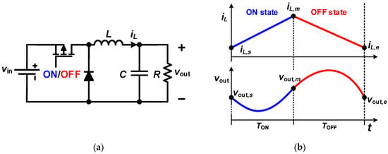
Figure 1.
Buck converter: (a) Circuit scheme and (b) inductor current and output voltage during switching-ON and switching-OFF.
In Figure 1a, L is the power inductance, R is the load resistance, C is the output capacitance, vin is the input voltage, vout is the output voltage, and iL denotes the inductor current. In each switching cycle (Figure 1b), the state variables begin with the initial state , and achieve the transition state at t = TON. They achieve the end-point state at time t = T = TON + TOFF.
With a fixed switching cycle, it is obvious that xe is a function of :
Since xe in one switching cycle is xs of the next switching cycle, i.e., , the discrete-time state space model of the converter is given by
Furthermore, the modeling accuracy is determined by the function at the right side of Equations (1) and (2), which will be derived by total differential equations of switching-ON and switching-OFF durations. First, state variables and their derivative values at switching transients are given as constrains to solve the differential equations. Second, differential equations of the inductor current and output voltage are solved for the switching-ON duration, which derive the relationship between xs and xm. Furthermore, differential equations for the switching-OFF duration are solved, which derive the relationship between xm and xe. Finally, the relationship between xs and xe is derived.
2.1. State Variables and Their Derivative Values at Switching Transients
For the buck converter, the state variables and their derivative values at switching transients are given in Figure 2, where the inductor current and output voltage at t = 0 are given by
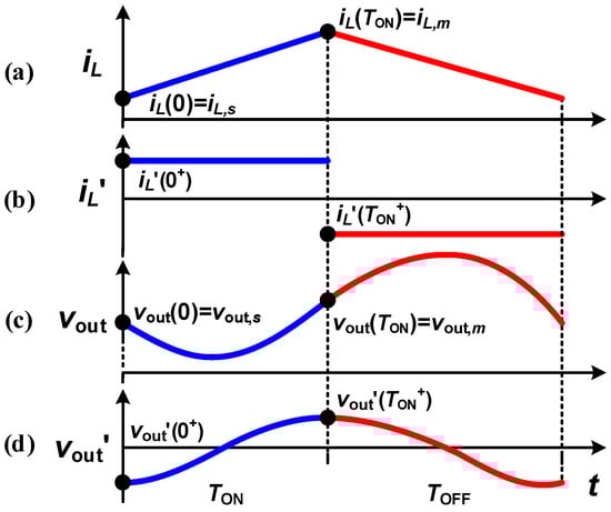
Figure 2.
State variables and their derivative values at switching transients: (a) Inductor current, (b) derivative of inductor current, (c) output voltage, and (d) derivative of output voltage.
Additionally, first-order derivatives of these parameters are determined by the instant voltage on the inductor and current through the capacitor. Therefore, at t = 0+, the derivative values and are given by
At t = TON, by continuity of the voltage and current signals, it is possible to write
At t = TON+, the instant voltage on the inductor and current through the capacitor are and , respectively. Therefore, derivatives of the current and voltage are given by
The aforementioned values will be used to solve differential equations of the inductor current and output voltage during switching-ON and switching-OFF, respectively.
2.2. Inductor Current and Output Voltage during Switching-ON
During switching-ON, the equivalent circuit scheme of the buck converter is as given in Figure 3. Since the voltage on the inductor and current across the capacitor are and , respectively, derivatives of the current and voltage are given by Equation (7).
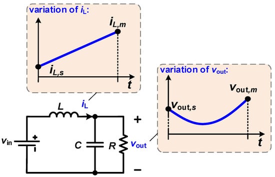
Figure 3.
Equivalent circuit scheme and state variations of the buck converter during switching-ON.
Using circuit laws and Equation (7), differential equations of and are given by
These second-order differential equations have the same characteristic roots, which are
Furthermore, explicit values of and are solved as
Taking Equations (3) and (4) into Equation (10) yields
Finally, substituting into Equation (10) gives , as shown in Equation (12).
This equation reveals the relationship between xs and xm, which is affected by .
2.3. Inductor Current and Output Voltage during Switching-OFF
During switching-OFF, the equivalent circuit scheme of the buck converter is as given in Figure 4. Since the voltage on the inductor and current across the capacitor are and , respectively, derivatives of the current and voltage are given by Equation (13).
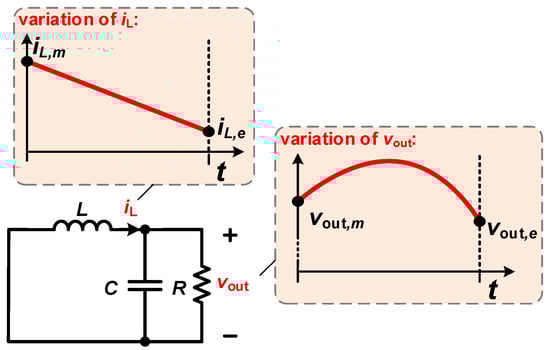
Figure 4.
Equivalent circuit scheme and state variations of the buck converter during switching-OFF.
Based on Equation (13), differential equations of and are given by
Obviously, Equation (14) has the same characteristic roots as Equation (8), and explicit values of and are solved as
Taking Equations (5) and (6) into Equation (15) gives
Furthermore, substituting t = TON + TOFF into Equation (15) gives , as shown in the following:
Combining Equation (12) and Equation (17), the relationship between xs and xe is derived as Equation (18):
where and are given in Equation (19). Furthermore, the variables in Equation (18) are listed in Table 1.

Table 1.
Variables in Equation (18).
Finally, since is always valid, the state equation of the proposed SSDM is given by
This model achieves a higher accuracy than that of conventional state-averaged models, which will be proved by the simulations in Section 4. Furthermore, the SSDM is used to derive the DPVP control strategy.
3. Digital Predictive Voltage Programmed Control
The scheme of the buck converter under DPVP control is given in Figure 5. The DPVP controller needs three Analog to Digital Converters (ADCs) ADCs to sample the input voltage, output voltage, and inductor current. The sampled values are used to calculate g2(d) with Equation (20). Furthermore, a look-up-table of is used to acquire the duty ratio from g2(d). Finally, the duty ratio is modulated through DPWM to control the buck converter.
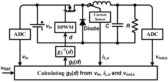
Figure 5.
Scheme of the buck converter under Digital Predictive Voltage Programmed (DPVP) control.
With DPVP control, vout,s should be regulated to vREF in one switching cycle, and the bandwidth of the controller is maximized. The DPVP control law, stability, and saturation issues are analyzed in the following.
3.1. DPVP Control Law
The DPVP controller calculates a suitable g2(d) and d to shape the output voltage. In an ideal condition, the output voltage can be regulated to track its reference in one switching cycle, as shown in Figure 6a. In the kth switching cycle, is valid, and the converter operates at a steady state. In the k + 1th switching cycle, the reference voltage steps up, which induces a positive voltage error. Furthermore, to eliminate the error, the duty ratio is increased, which ensures . Finally, the output voltage re-stabilizes in the k + 2th switching cycle. In this way, vout,s tracks vREF in one switching cycle, i.e., vout,s = vREFz−1.
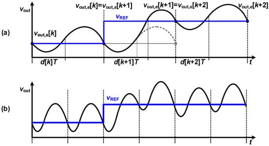
Figure 6.
Output voltage under DPVP control: (a) Ideal condition and (b) Matlab-Simulink simulation with a consideration of parasitics.
In a practical condition, with a consideration of parasitics, the output voltage tracks its reference value in three switching cycles, as shown in Figure 6b. The results are exported from a Matlab-Simulink simulation.
The DPVP control law is derived from the SSDM model. Based on Equation (20), the relationship between and is given by
Substituting the control object into Equation (21) gives
Furthermore, an inverse function is used to derive the duty ratio, which regulates to in one switching cycle.
3.2. Stability Analysis and Compensation for a DPVP Controlled Buck Converter
Based on Equation (22), the output voltage can be regulated to vREF in just one switching cycle. In this way, the control loop bandwidth is maximized. However, as a nonlinear control approach, the DPVP control law lacks integral items. This induces steady state error between vout,s and vREF. Besides, an extremely high bandwidth can degrade the robustness to parameter deviations. In order to eliminate the steady state error and improve the stability, an integral compensator IT/(z − 1) is used to reduce the bandwidth, which forms the control scheme in Figure 7a.
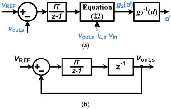
Figure 7.
DPVP control with integral compensation: (a) Control scheme and (b) closed-loop equivalent model.
Furthermore, the closed-loop equivalent model is given in Figure 7b, and the closed-loop transfer function from vREF to vout,s is given by
Equation (23) has two poles located at . When IT varies from 0 to 1, the variations of the poles are as given in Figure 8. When IT < 1/4, both poles are real, and the bandwidth is degraded by the lower pole. When IT ≥ 1/4, the poles become conjugated to the real axis. As IT increases, the poles move toward the unit cycle, leading to a degraded stability. In order to improve the bandwidth while maintaining the stability, IT should be near to 0.35 when the damping factor is 0.7 and the closed-loop bandwidth is 0.25π/T. The achieved bandwidth is relatively high for DC-DC converters operating in CCM.
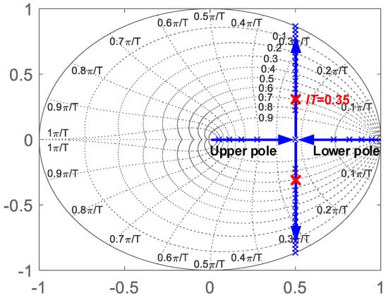
Figure 8.
Root locus of Φ(z) when IT changes from 0 to 1.
3.3. Saturation of DPWM
Switched mode power converters are nonlinear systems, where the large-signal performance is limited by DPWM saturation. With DPVP control, the output of might be greater than unity or lower than zero, which leads to the saturation of DPWM. The saturation issue limits the physical-achievable slew rate of the output voltage and leads to potential instability. Therefore, the input of the integral compensator is limited to eliminate the DPWM saturation, which derives the practical control scheme in Figure 9.
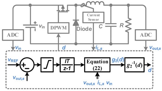
Figure 9.
Practical DPVP controller with integral compensation and eliminated DPWM saturation.
Since the achievable duty ratio is between zero and unity, the output voltage of the converter has a limited slew rate. For the buck converter, the output voltage increases along the duty ratio. The variation of the output voltage in one switching cycle reaches its maximum value when d = 1 and reaches its minimum value when d = 0. Therefore, the output voltage slew rate is limited by either d = 1 or d = 0, as shown in Figure 10.
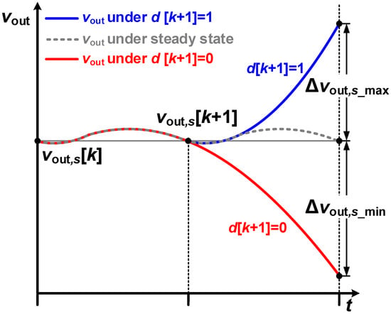
Figure 10.
Output voltage under a steady state, where d[k + 1] = 1 and d[k + 1] = 0.
Based on Equation (20), the initial voltage of the next switching cycle is given by
Therefore, the variation of vout,s in one switching cycle is
The magnitude reaches its maximum value when d = 1 and reaches its minimum value when d = 0, as shown in Equation (26).
Therefore, the output voltage slew rate is limited between and , as shown in the following:
To avoid potential oscillation, this physical saturation should be avoided in the controller design. Since the slew rate is limited by the input of the integral compensator, Equation (28) is applied to the controller.
In this way, physical saturation of DPWM is avoided, which eliminates potential oscillations.
4. Simulations
Simulations were carried out in Matlab to verify the proposed SSDM and DPVP control strategy. The main specifications of the buck converter were the same as presented in Section 5. In the following, the accuracy of SSDM is proved by comparisons to a circuit model and a State Averaged Discrete-time Model (SADM). Additionally, the converter stability under DPVP control is verified through frequency response analyses.
4.1. Accuracy of SSDM
In order to verify the accuracy of the proposed SSDM, frequency response analyses were carried out for the SSDM, SADM, and circuit model. The SADM was derived by the Tustin method, which has a higher accuracy than forward and backward methods. The circuit model was constructed by circuit elements, and was used as a reference model. The analyses are given for output voltage responses from the duty ratio, input voltage, and load resistance.
As shown in Figure 11, for the frequency response from d to vout,s, the SADM deviates from the circuit model at a medium and high frequency. The phase error is relatively large, especially at a high frequency, which results in degraded controller design and low-accuracy stability analysis. When 30k ≤ ω < 100k rad/s, the phase error varies from 3.5 to 11 degrees. When ω ≥ 100k rad/s, the phase error is even larger. For SSDM, both the magnitude and phase highly match those of the circuit model.
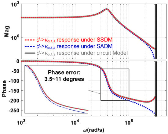
Figure 11.
Frequency response from d to vout,s under the State Switched Discrete-time Model (SSDM), State Averaged Discrete-time Model (SADM), and circuit model.
As shown in Figure 12, for the frequency response from vin to vout,s, the SADM also deviates from the circuit model at a medium and high frequency. When 30 k ≤ ω < 100 k rad/s, the phase error varies from 6 to 21 degrees. When ω ≥ 100 k rad/s, the phase error is even larger. For SSDM, both the magnitude and phase highly match those of the circuit model.
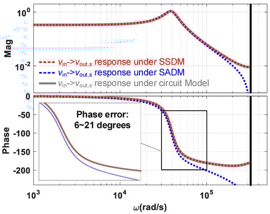
Figure 12.
Frequency response from vin to vout,s under the SSDM, SADM, and circuit model.
As shown in Figure 13, for the frequency response from R to vout,s, the SADM deviates from the circuit model at a medium frequency. When 30 k ≤ ω < 100 k rad/s, the phase error varies from 2 to 2.5 degrees, which is relatively small. For SSDM, both the magnitude and phase highly match those of the circuit model.
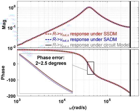
Figure 13.
Frequency response from R to vout,s under the SSDM, SADM, and circuit model.
4.2. Stability under DPVP Control
According to the analyses in Section 3, the DPVP controller regulates the output voltage to the reference voltage in one switching cycle, i.e., . Additionally, an integral compensator is used to compensate for the loop, which improves the stability and eliminates the steady state error of the output voltage. In order to validate the performance under DPVP control, frequency responses were investigated for the circuit model and the equivalent model, respectively.
Open-loop frequency analyses were conducted for transients, and the results were compared to verify if tracks in one switching cycle. As shown in Figure 14a, the frequency response of the circuit model highly matches that of the equivalent model. Without integral compensation, the output voltage under DPVP control tracks in one switching cycle.
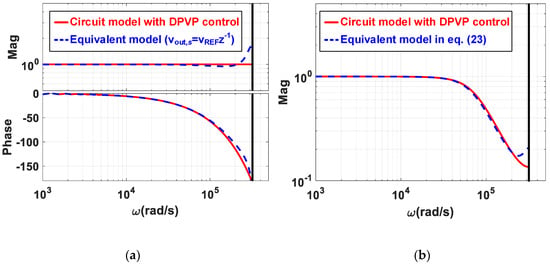
Figure 14.
Frequency responses of the circuit model and the equivalent model: (a) Open-loop analysis for the transient without integral compensation and (b) closed-loop analysis for the transient with integral compensation.
In order to eliminate the steady state error and improve the stability, an integral compensator was used to reduce the bandwidth. The closed-loop analyses are given in Figure 14b, where the integral parameter is set as I = 0.35/T. It is obvious that the frequency response of the equivalent model highly matches that of the circuit model. Additionally, no frequency spike is found in the plot, which proves the closed-loop stability under DPVP control.
4.3. Stability Regarding Deviated Inductance
Furthermore, the stability was proven in terms of deviated inductance. Suppose that the actual inductance in the converter is La, while the controller is set with an inductance of L. When La changes from 0.9 to 1.6 L, the closed-loop frequency analyses for the , , and transients are as plotted in Figure 15, Figure 16 and Figure 17, respectively.
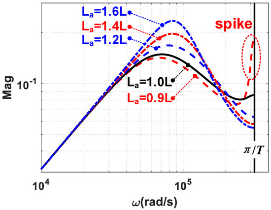
Figure 15.
Closed-loop frequency analyses under DPVP control for the R -> vout,s transient with deviated inductance.
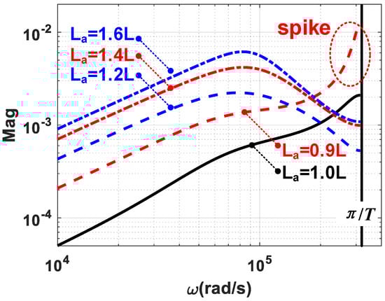
Figure 16.
Closed-loop frequency analyses under DPVP control for the vin -> vout,s transient under deviated inductance.
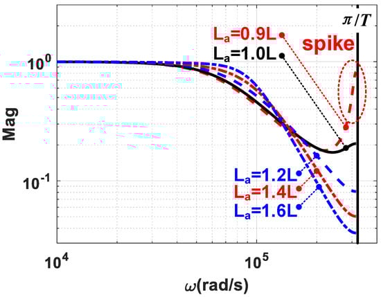
Figure 17.
Closed-loop frequency analyses under DPVP control for the vREF -> vout,s transient under deviated inductance.
According to Figure 15, all plots have a decreasing magnitude in a low-frequency range. The near derivative responses indicate zero DC gain, so the output voltage DC value is immune to the load. When La = 0.9 L, high-frequency oscillation occurs, since a frequency spike is found near π/T. As La increases, the magnitude decreases at a high frequency and increases around ω = 105 rad/s. This indicates a degraded medium frequency performance, while high-frequency oscillation is eliminated.
Figure 16 indicates that the output voltage exhibits little change when the input voltage varies, since all of the magnitudes are very small. Moreover, all plots are derivative in a low-frequency range. Therefore, the output voltage DC value is immune to the input voltage. However, high-frequency oscillation might occur when La is smaller than L, as indicated by the frequency spike at π/T. When La = L, the response has the lowest magnitude and it is near-derivative in all frequency ranges. As La increases, the magnitude of the response increases, which indicates larger deviation during the transient.
As shown in Figure 17, the bandwidth of the converter increases along La. Furthermore, high-frequency oscillation occurs when La = 0.9 L, since a frequency spike is found near π/T.
All simulations indicate that potential high-frequency oscillation might occur when La = 0.9 L, while the performance is slightly degraded when La is larger than L. To avoid potential high-frequency oscillations, a practical solution is to design the controller under La = (1.1–1.2) L.
5. Experiments
Experimental results are given to verify the effectiveness of the proposed DPVP controller. The main specifications of the buck converter are shown in Table 2. The specifications are designed to achieve a typical power rate of 5 W, a current ripple rate of ±0.35, and an output voltage ripple rate below 1%. The input/output voltages are selected for point-of-load applications, USB chargers, and an embedded system power supply, etc.
Table 2.
Specifications of the buck converter.
A photograph of the prototype is given in Figure 18. An FPGA (Cyclone IV) control board is used to carry out digital control algorithms. The output and input voltages are sampled by ADC (LTC2314-14) modules. A main switch MOSFET (FDS86540) and a diode (NRVTSA4100E) are used as switching components. The output capacitor adopts two 10 µF capacitors (KRM55QR71J106KH01K) connected in parallel. The core material of the inductor is NPH107060, which is adequate for a switching frequency below 200 kHz.
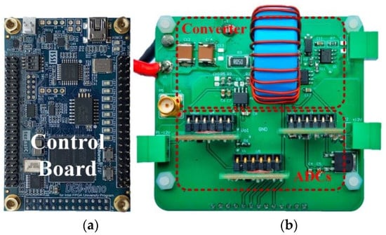
Figure 18.
The experimental prototype: (a) Control board and (b) buck converter.
The output voltage was measured under disturbances of load, input voltage, and reference voltage. The results under DPVP control were compared with those of a digital current mode controller with Proportional Integral Derivative (PID) PID compensation in the outer loop. For the digital current mode controller, the PID compensator was optimized through the PID tuner toolbox in Matlab. It was designed with a phase margin of 75 degrees and the cross-over frequency was 30k rad/s. Furthermore, the robustness of the system under DPVP control was verified under deviated inductance.
5.1. Output Voltage Transient Responses
As shown in Figure 19a, when the load resistance steps from 10 to 5 Ω, the output voltage deviates by −0.6 V and re-stabilizes in 130 μs under digital current mode control with PID compensation. According to the analyses in Section 4, the closed-loop frequency response of the load transient is near-derivative in a low-frequency range and near-integrative in a high-frequency range. The response approximates a typical second-order system with a nature frequency of 70 k rad/s. Therefore, with a damping factor of 0.7, the output voltage should re-stabilize in 36 μs. As shown in Figure 19b, the experimental results match with those of the analysis. The output voltage deviates by −0.3 V and re-stabilizes in 40 μs.
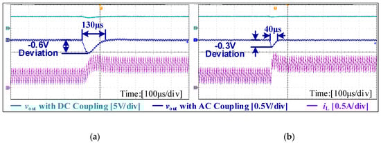
Figure 19.
Transient voltage and current when R steps from 10 to 5 Ω: (a) Digital current mode control with PID compensation and (b) DPVP control.
As shown in Figure 20a, when the input voltage steps from 12 to 9.5 V, the output voltage drops by 0.8 V and re-stabilizes in 200 μs under digital current mode control with PID compensation. According to Figure 16, the frequency response under DPVP control is near-derivative in all frequency ranges and the magnitude is very low. This indicates a strong rejection to input voltage disturbance. As shown in Figure 20b, the experimental result matches that of the analysis. When the input voltage steps from 12 to 9.5 V, the output voltage deviates by −0.2–0.15 V and re-stabilizes in 60 μs.
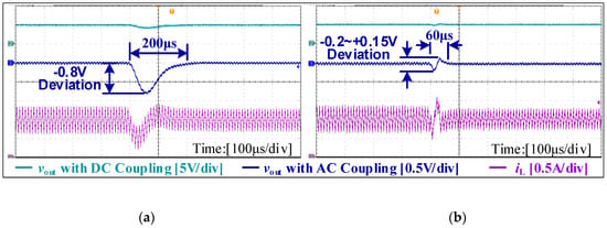
Figure 20.
Transient voltages and current when vin steps from 12 to 9.5 V: (a) Digital current mode control with PID compensation and (b) DPVP control.
When the reference voltage steps from 5 to 6 V, the output voltage tracks it in 150 μs under digital current mode control with PID compensation. According to the analyses in Section 4, the bandwidth of the closed-loop system is about 65 k rad/s. Therefore, with a damping factor of 0.7, the output voltage should reach the reference value in 38 μs. The experimental result matches that of the analysis, as shown in Figure 21b. The output voltage reaches the reference voltage in 30 μs, which is five times faster than that of digital current mode control.
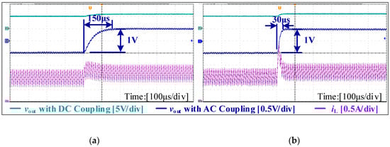
Figure 21.
Transient voltages and current when steps from 5 to 6 V: (a) Digital current mode control with PID compensation and (b) DPVP control.
5.2. The Robustness to Deviated Inductance
According to the closed-loop analyses in Section 4, the converter remains stable when La deviates from 0.9 to 1.6 L. However, high-frequency oscillation might occur when La is smaller than L. When La is larger than L, although the performance is slightly degraded, the high-frequency oscillation is eliminated. Therefore, La can be set a little higher than L to improve the robustness to deviated inductance. In the following, experimental results are given when La deviates to 1.3 and 1.6 L, respectively.
When the load resistance steps from 5 to 10 Ω, the output voltage transients are as given in Figure 22. With La = 1.3 L and La = 1.6 L, the output voltage suffers from a degraded transient performance. The response time increases to 60 and 70 μs, respectively. When the input voltage steps from 12 to 9.5 V, the output voltage transients are as given in Figure 23. The transient response time increases to 70 and 90 μs, respectively. When the reference voltage steps from 5 to 6 V, the output voltage transients are as given in Figure 24. The output reaches the reference voltage and stabilizes in 50 and 100 μs, respectively. Although the transient responses are degraded with a deviated inductance, the output voltage is still stable when La = 1.6 L. The results indicate a high robustness of DPVP control to inductance deviation.
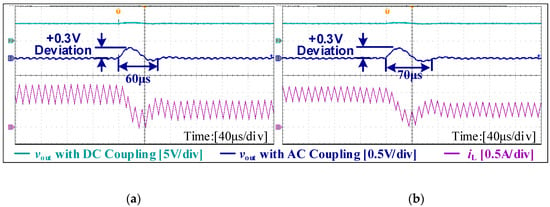
Figure 22.
Output voltage transients under DPVP control when R steps from 5 to 10 Ω: (a) La = 1.3 L and (b) La = 1.6 L.
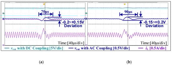
Figure 23.
Output voltage transients under DPVP control when vin steps from 12 to 9.5 V: (a) La = 1.3 L and (b) La = 1.6 L.
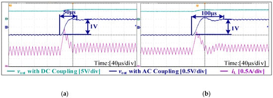
Figure 24.
Output voltage transients under DPVP control when vREF steps from 5 to 6 V: (a) La = 1.3 L and (b) La = 1.6 L.
All results match those of the analyses and simulations, and prove the effectiveness of the proposed DPVP control strategy.
6. Conclusions
This paper proposes a State Switched Discrete-time Model and Digital Predictive Voltage Programmed controller for a buck converter operating in continuous conduction mode. Compared with the conventional state-averaged modeling method, the SSDM considers the variation of states within a switching cycle, and it achieves a higher accuracy at a medium and high frequency. Furthermore, based on SSDM, a DPVP control law is proposed that regulates the output voltage to its reference value in one switching cycle. Finally, with an integral compensation and saturation limit for DPWM, a practical DPVP control strategy exhibits a high stability and achieves very fast transient responses.
The accuracy of SSDM has been proven by simulations, which were compared with the conventional state averaged discrete-time model and the circuit model. The stability and robustness under DPVP control was proven by open-loop and closed-loop frequency analyses. Finally, the effectiveness of the DPVP controller and the robustness to deviated inductance were verified through experiments.
Author Contributions
Conceptualization and methodology, R.M.; project administration, Q.T.; resources, Q.Z.; software and validation, G.S.; supervision, Z.L.; writing—review and editing, W.W. All authors have read and agreed to the published version of the manuscript.
Funding
This work was funded by the National Natural Science Foundation of China under Grant 61701184.
Acknowledgments
This work is supported by the Shanghai Institute of Satellite Engineering and Huazhong University of Science and Technology.
Conflicts of Interest
The authors declare no conflicts of interest.
List of Symbols
| xs, xm, xe | States of the converter at the initial, transition, and end points in a switching cycle |
| vin, vout | Input and output voltages |
| vout,s, vout,m, vout,e | Output voltage at the initial, transition, and end points in a switching cycle |
| vREF | Reference for the output voltage |
| iL | Inductor current |
| iL,s, iL,m, iL,e | Inductor current at the initial, transition, and end points in a switching cycle |
| d, T | Duty ratio and switching cycle of DPWM |
| TON, TOFF | ON and OFF time in a switching cycle |
| L, R, C | The power inductance, load resistance, and output capacitance |
| a11, a12, a21, a22, b1, b2, g1(d), g2(d) | Parameters in the proposed SSDM |
| Φ(z) | Closed-loop transfer function from vREF to vout,s |
| ∆vout,s | Variation of vout,s in one switching cycle |
| I | Gain of the integral compensator |
References
- Cheng, K.-Y.; Yu, F.; Lee, F.C.; Mattavelli, P. Digital enhanced V2-type constant on-time control using inductor current ramp estimation for a buck converter with low-ESR capacitors. IEEE Trans. Power Electron. 2013, 28, 1241–1252. [Google Scholar] [CrossRef]
- Cortés, J.; Šviković, V.; Alou, P.; Oliver, J.A.; Cobos, J.A.; Wisniewski, R. Accurate analysis of subharmonic oscillations of V2 and V2Ic controls applied to buck converter. IEEE Trans. Power Electron. 2015, 30, 1005–1018. [Google Scholar] [CrossRef]
- Tian, S.; Lee, F.C.; Li, Q.; Yan, Y. Unified equivalent circuit model and optimal design of V2 controlled buck converters. IEEE Trans. Power Electron. 2016, 31, 1734–1744. [Google Scholar] [CrossRef]
- Meyer, E.; Liu, Y. Digital charge balance controller with an auxiliary circuit for improved unloading transient performance of buck converters. IEEE Trans. Power Electron. 2013, 28, 357–370. [Google Scholar] [CrossRef]
- Jia, L.; Liu, Y. Low cost microcontroller based implementation of robust voltage based capacitor charge balance control algorithm. IEEE Trans. Ind. Inform. 2013, 9, 869–879. [Google Scholar] [CrossRef]
- Ling, R.; Maksimovic, D.; Leyva, R. Second-order sliding-mode controlled synchronous buck DC–DC converter. IEEE Trans. Power Electron. 2016, 31, 2539–2549. [Google Scholar] [CrossRef]
- Dashtestani, A.; Bakkaloglu, B. A fast settling oversampled digital sliding-mode DC–DC converter. IEEE Trans. Power Electron. 2015, 30, 1019–1027. [Google Scholar] [CrossRef]
- Gautam, A.R.; Gourav, K.; Guerrero, J.M.; Fulwani, D.M. Ripple mitigation with improved line-load transients response in a two-stage DC–DC–AC converter: Adaptive SMC approach. IEEE Trans. Ind. Electron. 2018, 65, 3125–3135. [Google Scholar] [CrossRef]
- Repecho, V.; Masclans, N.; Biel, D. A comparative study of terminal and conventional sliding mode start-up peak current controls for a synchronous buck converter. IEEE J. Emerg. Sel. Top. Power Electron. 2019. [Google Scholar] [CrossRef]
- Vidal-Idiarte, E.; Restrepo, C.; El Aroudi, A.; Calvente, J.; Giral, R. Digital control of a buck converter based on input-output linearization. An interpretation using discrete-time sliding control theory. Energies 2019, 12, 2738. [Google Scholar] [CrossRef]
- Chen, J.; Prodic, A.; Erickson, R.W.; Maksimovic, D. Predictive digital current programmed control. IEEE Trans. Power Electron. 2003, 18, 411–419. [Google Scholar] [CrossRef]
- Restrepo, C.; Konjedic, T.; Flores-Bahamonde, F.; Vidal-Idiarte, E.; Calvente, J.; Giral, R. Multisampled digital average current controls of the versatile buck–boost converter. IEEE J. Emerg. Sel. Top. Power Electron. 2019, 7, 879–890. [Google Scholar] [CrossRef]
- Zhang, Q.; Min, R.; Tong, Q.; Zou, X.; Liu, Z.; Shen, A. Sensorless predictive current controlled DC-DC converter with a self-correction differential current observer. IEEE Trans. Ind. Electron. 2014, 61, 6747–6757. [Google Scholar] [CrossRef]
- López, F.; López-Martín, V.M.; Azcondo, F.J.; Corradini, L.; Pigazo, A. Current-sensorless power factor correction with predictive controllers. IEEE J. Emerg. Sel. Top. Power Electron. 2019, 7, 891–900. [Google Scholar] [CrossRef]
- Buso, S.; Caldognetto, T.; Brandao, D.I. Dead-beat current controller for voltage-source converters with improved large-signal response. IEEE Trans. Ind. Appl. 2016, 52, 1588–1596. [Google Scholar] [CrossRef]
- Zhang, X.; Wang, B.; Tan, X.; Gooi, H.B.; Iu, H.H.; Fernando, T. Deadbeat control for single-inductor multiple-output DC-DC converter with effectively reduced cross regulation. IEEE J. Emerg. Sel. Top. Power Electron. 2019. [Google Scholar] [CrossRef]
- Cuoghi, S.; Mandrioli, R.; Ntogramatzidis, L.; Gabriele, G. Multileg interleaved buck converter for EV charging: Discrete-time model and direct control design. Energies 2020, 13, 466. [Google Scholar] [CrossRef]
- Min, R.; Lyu, D.; Cheng, S.; Sun, Y.; Li, L. Linearized discrete charge balance control with simplified algorithm for DCM buck converter. Energies 2019, 12, 3177. [Google Scholar] [CrossRef]
- Maksimovic, D.; Zane, R. Small-signal discrete-time modeling of digitally controlled PWM converters. IEEE Trans. Power Electron. 2007, 22, 2552–2556. [Google Scholar] [CrossRef]
- Li, X.; Ruan, X.; Xiong, X.; Sha, M.; Tse, C.K. Approximate discrete-time small-signal models of DC–DC converters with consideration of practical pulsewidth modulation and stability improvement methods. IEEE Trans. Power Electron. 2019, 34, 4920–4936. [Google Scholar] [CrossRef]
- Zurbriggen, I.G.; Ordonez, M.; Anun, M. PWM-geometric modeling and centric control of basic DC-DC topologies for sleek and reliable large-signal response. IEEE Trans. Ind. Electron. 2015, 62, 2297–2308. [Google Scholar] [CrossRef]
- Kumar, V.I.; Kapat, S. Unified digital current mode control tuning with near optimal recovery in a CCM buck converter. IEEE Trans. Power Electron. 2016, 31, 8461–8470. [Google Scholar] [CrossRef]
- Karamanakos, P.; Geyer, T.; Manias, S. Direct voltage control of DC-DC boost converters using enumeration-based model predictive control. IEEE Trans. Power Electron. 2014, 29, 968–978. [Google Scholar] [CrossRef]
- Yue, X.; Wang, X.; Blaabjerg, F. Review of small-signal modeling methods including frequency-coupling dynamics of power converters. IEEE Trans. Power Electron. 2019, 34, 3313–3328. [Google Scholar] [CrossRef]


© 2020 by the authors. Licensee MDPI, Basel, Switzerland. This article is an open access article distributed under the terms and conditions of the Creative Commons Attribution (CC BY) license (http://creativecommons.org/licenses/by/4.0/).