Modified Impedance-Source Inverter with Continuous Input Currents and Fault-Tolerant Operations


1
Department of Energy Technology, Aalborg University, 9220 Aalborg, Denmark
2
College of Electrical and Information Engineering, Hunan University, Changsha 410082, China
3
Department of Engineering-Electrical Engineering Division, University of Cambridge, Cambridge CB3 0FA, UK
*
Author to whom correspondence should be addressed.
Energies 2020, 13(13), 3408; https://doi.org/10.3390/en13133408
Submission received: 28 May 2020
/
Revised: 18 June 2020
/
Accepted: 26 June 2020
/
Published: 2 July 2020
(This article belongs to the Special Issue Emerging Converters, Advanced Control and Technologies Enhancing Electric Energy Conversion in Photovoltaic Systems)
Abstract
:Impedance-source (Z-source) inverters are increasingly adopted in practice, where a high voltage gain is required. However, issues like drawing a non-continuous current from the DC source and ceasing the energy supply under DC source faults are also observed. In this paper, an embedded enhanced-boost Z-source inverter (EEB-ZSI) is thus proposed to tackle the issues. The proposed EEB-ZSI employs two DC sources, which enable the continuous input current and fault-tolerant operations (e.g., open-circuit and short-circuit faults in the DC sources). The operational principles are presented in detail with an in-depth circuit analysis. Moreover, the proposed EEB-ZSI is benchmarked with prior-art Z-source inverters. Experimental tests further demonstrate the effectiveness of EEB-ZSI regarding the continuous input current and flexible fault tolerance.
1. Introduction
Impedance source (Z-source) inverters are becoming promising in industrial applications, e.g., photovoltaic and fuel cell systems, because of their superior performance [1,2,3,4,5,6,7]. Conventionally, voltage source inverters (VSI) can only operate in buck operation. To address this issue, Z-source inverters, e.g., the Z-source inverter (ZSI) [8], with a larger boost ratio were introduced in the literature. Notably, a shoot-through state is added into the traditional modulation algorithm. In addition, the application of impedance-source inverters reduces the overall system cost and improves the efficiency as a single-stage power conversion solution to some extent [7]. Nevertheless, ZSIs have certain drawbacks. For example, they may draw a discontinuous input current, attain a large voltage stress across the component, and result in a poor power quality [9]. These hinder the applications of ZSI systems to some extent. Hence, tremendous efforts have been made in the literature to improve the performance and applicability of ZSI, generally through topological innovations and advanced modulation algorithms. As a representative topology among the prior-art ZSIs, the quasi Z-source inverter (qZSI) provides an effective solution to the above drawbacks [10]. Thus, many explorations of the qZSI have been presented in the literature in terms of modulation strategies to improve the efficiency and reliability.
At the same time, a vast array of impedance-source networks has been introduced to further improve the boosting capability, while also addressing the above limitations. Clearly, increasing the voltage gain could be attained by applying more passive components or active switches to the basic Z-source network, as indicated in Figure 1a. With this principle, switched-inductor (SI) or switched-capacitor (SC) cells can be used to replace the inductors or capacitors in the original ZSI or qZSI, thus leading to a higher boost ratio [11,12]. For instance, SI cells are placed in the qZSI to ensure continuous input current and low voltage stress [13]. Nevertheless, more passive components makes the inverter volume much larger compared to the basic Z-source inverter.
Additionally, the voltage gain can be increased by cascading the impedance-source networks. To achieve superior performance in terms of boosting capability and low voltage stresses across the components, the extended-boosted ZSI topologies were proposed in [14,15]. In addition, from [16], several enhanced-boost ZSIs (EB-ZSI) in Figure 1b are presented, and an enhanced boosting capability can be achieved in contrast to the topologies in [14,15]. However, the major drawbacks of these topologies are discontinuous input current and large starting inrush current. It should be noted that the performance of renewable energy systems is closely related to the input current waveform. In a fuel cell system, high ripple input current might lead to an increment of the fuel consumption, so the overall efficiency is degraded [17]. Moreover, the converters with continuous input currents are more promising in PV systems considering the accuracy of the maximum power point tracking (MPPT) [18]. Therefore, the converters with continuous input currents are welcome to be applied in the low voltage scenario to suppress the stress and improve the lifetime of the voltage source. Accordingly, a modified qZSI inverter with two switched impedance networks was introduced in [19]. This topology features a continuous input current and lower voltage stresses over the components due to its common ground between the source and bridge.
Furthermore, the DC current of the ZSI is normally chopped due to the existence of the diodes, as observed in Figure 1a. To address this, embedded Z-source inverters were proposed [20,21,22], as exemplified in Figure 2. It can be seen in Figure 2 that an embedded ZSI (E-ZSI) has two DC sources, which are directly connected in series with the inductors of the conventional ZSI shown in Figure 1a. In [22], the embedded sources were further developed into the asymmetrical and symmetrical structures depending on the embedded source position, which can achieve implicit source current or voltage filtering without extra hardware. Although the above embedded ZSIs can overcome certain drawbacks, which exist in the conventional Z-source inverter, no significant improvement can be achieved regarding the boost capability.
Beyond topological and modulation improvements, the fault-tolerant capability is of high concern in practical applications to ensure the security of power supply. The prior-art impedance source topologies with fault-tolerance capabilities were only paying attention to power switch failures. For example, Ref. [23] introduced a topology that includes two symmetrical quasi-Z-source networks and a T-type inverter. Then, the modified modulation scheme can be used to achieve the fault-tolerance operations without applying additional phase legs to the main topology. In addition, Ref. [24] introduced a modified topology, which can operate in the abnormal conditions by using two legs. However, apart from switch failures, DC source failures may also occur practically, leading to system shutdown and interrupted power supply. For instance, in PV applications, the two DC sources may produce different currents due to shading [25]. Even for single-source impedance-source networks, low DC voltage or open-circuit faults may happen. However, the above topologies have to cease energizing the load in these cases. Thus, to ensure secure power supply, continuous input current, and also high boost gain, advanced impedance-source networks should be developed for PV applications.
In light of all the previous limitations, this paper introduces a topology with continuous input current and fault-tolerance capabilities, while maintaining a high boosting ratio. The proposed embedded enhanced-boost Z-source inverter (EEB-ZSI) is based on the embedded Z-source and switched impedance-source networks. Consequently, the proposed EEB-ZSI not only inherits the superior high boost capability of the switched impedance inverters, but also achieves continuous input current and lower voltage stress of the capacitors. Moreover, it is revealed in this paper that the proposed EEB-ZSI can maintain a normal operation even if the DC sources are in abnormal conditions. The rest of the paper is organized as follows. The operation principle, the comparison in terms of boosting capability and voltage stress on switches and capacitors, among various topologies, and the parameter design of EEB-ZSI are presented in Section 2. The fault-tolerant operation is then analysed in detail in Section 3. Section 4 provides the experimental results to validate the effectiveness of the theoretical analysis. Finally, the concluding remarks are presented in Section 5.
2. Proposed Embedded Enhanced-Boost Z-Source Inverter
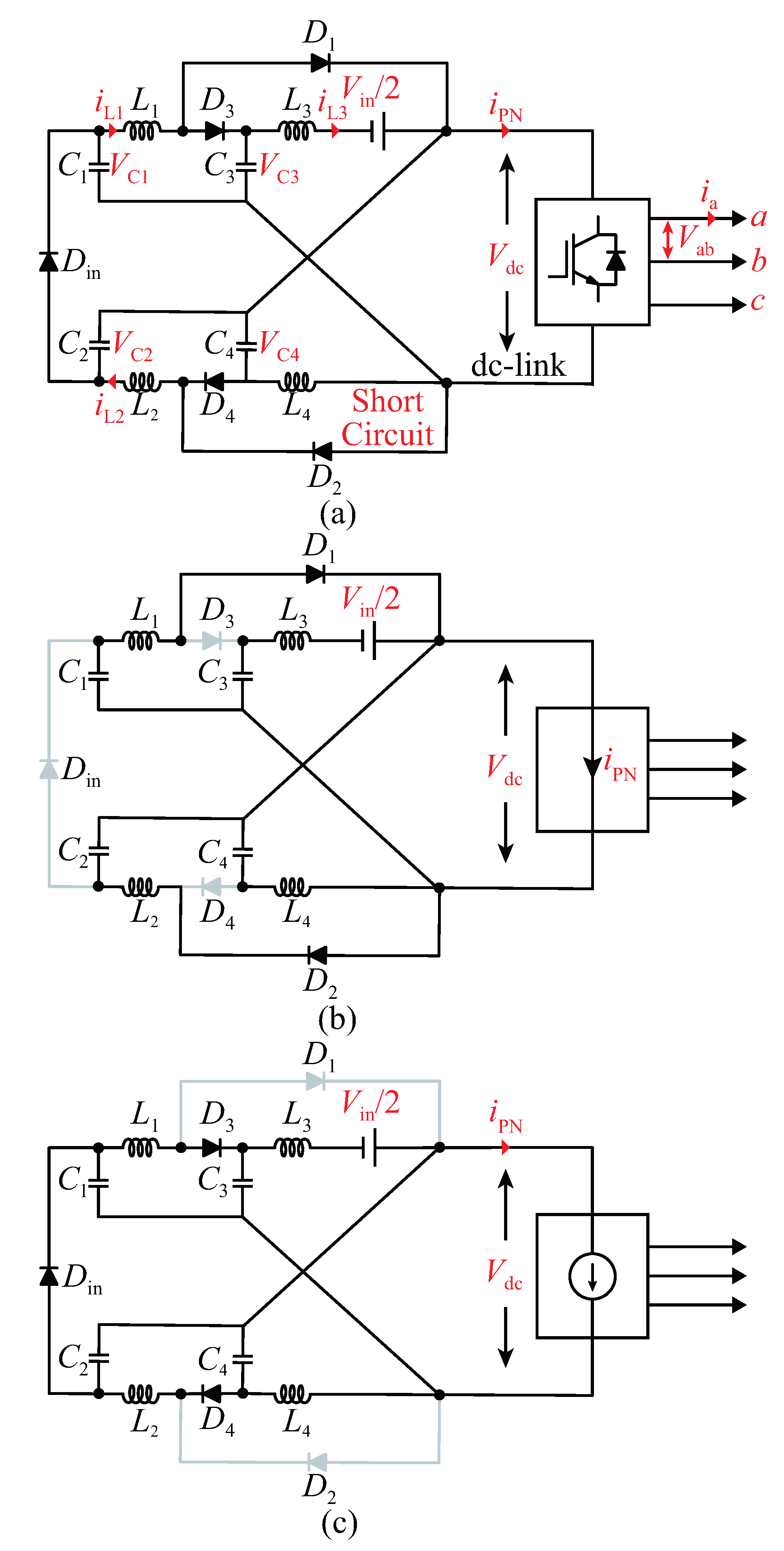
As indicated in Figure 3a, EEB-ZSI has two DC sources, which are inserted into the impedance-source network. In this section, the operation principle, the comparison of the boost capability, the voltage stresses, and the design considerations are presented.
2.1. Operation Principle
As observed in Figure 3a, two switched Z-source networks are arranged in a symmetrical way, and there are two input voltage sources in the proposed EEB-ZSI.
All the inductors are defined as , , , and ; all the capacitors are expressed as , , , and ; all the diodes are denoted as , , , , and .
Similar to the basic ZSI, the operation principle of EEB-ZSI can be classified into two states—the shoot-through (ST) state and the non-shoot-through (NST) state. The equivalent circuits of EEB-ZSI in the ST state and NST state are presented in Figure 3b,c, respectively. The same components in EEB-ZSI are presumed to be the same parameters. Furthermore, the input DC source voltage in EEB-ZSI is identical to the voltage being . According to the topological symmetry, it can be obtained that
in which , , , and are the corresponding voltages across the capacitors , , , and and , , , and are the corresponding currents flowing through the inductors , , , and . According to the previous analysis, there are two operation states:
ST State: In this case, Figure 3b shows that the DC side of the inverter is short-circuited by turning on the switches in each inverter leg simultaneously. and are the ON-state with , , and being reverse-biased during the ST state. The inductors are charged by the capacitors, and no power is delivered to the AC side (the load). Then, it can be obtained that:
where and are the voltage of the inductor and in the ST state. Based on Kirchoff’s voltage law (KVL), the inductor voltages and can be expressed as:
According to the volt-second balance principle, they can be derived:
where , , and are the inductor voltages on , , and , respectively, during the NST state and D is the duty cycle. According to Equations (5)–(10), it can be derived that:
NST State: It can be observed from Figure 3c that , , and are the ON-state and and are the OFF-state. During this state, the capacitors are charged, and the load is supplied through the inverter. In addition, based on Figure 3c, the following equations can be derived by applying KVL:
where is the peak DC-link voltage. Substituting (11) into (14), then it can be obtained that:
Then, the capacitor voltage and the peak DC-link voltage can be given as:
where:
is the boost factor. Therefore, the average DC-link voltage of the inverter can be expressed as:
The peak of the inverter output voltage can be given as:
in which G is the buck-boost factor and M is the modulation index. Then, the buck-boost factor can be obtained in regards to M as:
Following the above analysis, the relationship between the inductor currents and the peak DC-link current can be obtained as:
2.2. Boost Capability Comparison
Figure 4a presents the relationship of the boost factor versus the ST duty ratio among conventional ZSI [8], embedded-ZSI (E-ZSI) [20], diode-assisted ZSI (DA-ZSI) [15], switched-inductor ZSI (SI-ZSI) [11], EB-ZSI [16], and EEB-ZSI. This can be observed in Figure 4a, where the boost factor of EEB-ZSI is much larger than the other selected ZSIs owing to the extra inductors except EB-ZSI. Moreover, Figure 4b presents the relationship between the voltage gains of the selected topologies and the modulation index. The voltage gain of EEB-ZSI is higher than most of the topologies in certain ranges of the modulation index. It should be pointed out that the power quality is associated with the modulation index, and better quality might be achieved with a high modulation index. Thus, to achieve the same voltage gain, EEB-ZSI and EB-ZSI can have a higher modulation index when compared with other topologies.
2.3. Voltage Stresses Comparison
Apart from the superior boost capability of the proposed EEB-ZSI, lower voltage stresses of EEB-ZSI are another advantage, as shown in Figure 5. The voltage stresses are specified as the proportion of the peak DC-link voltage and capacitors’ voltages to the minimum DC voltage [26]. In Figure 5a, the proposed EEB-ZSI has lower voltage stresses across the switches than other selected ZSIs. Moreover, Figure 5b presents a comparison regarding the capacitor stress between EB-ZSI and EEB-ZSI. Here, the stresses across the capacitors in EEB-ZSI are lower than EB-ZSI under the same voltage gain, and thus, the performance in terms of cost and size can be improved by applying the capacitors with lower ratings. Additionally, Table 1 summarizes the benchmarking results in terms of boost factor, voltage gain, switch stress, and capacitor stresses.
2.4. Inductor and Capacitor Design
Based on the previous analysis, the capacitors charge the inductors, and the inductor currents increase linearly in the ST state. The inductor voltages during the ST state are presented as:
When the simple boost pulse-width modulation method is applied, there are two ST states in one switching cycle. Thus, the time interval of one ST is . Then, the inductors can be designed as:
with being the switching frequency and and representing the ripple currents. Similarly, the capacitors can be obtained as:
in which and are the voltage ripples for the capacitors , and , , respectively. Notably, the ripple voltage and current on the capacitors and inductors should be determined, respectively. Subsequently, according to Equations (28)–(31), the inductors and capacitors of the proposed impedance-source network can be designed.
2.5. Control Method
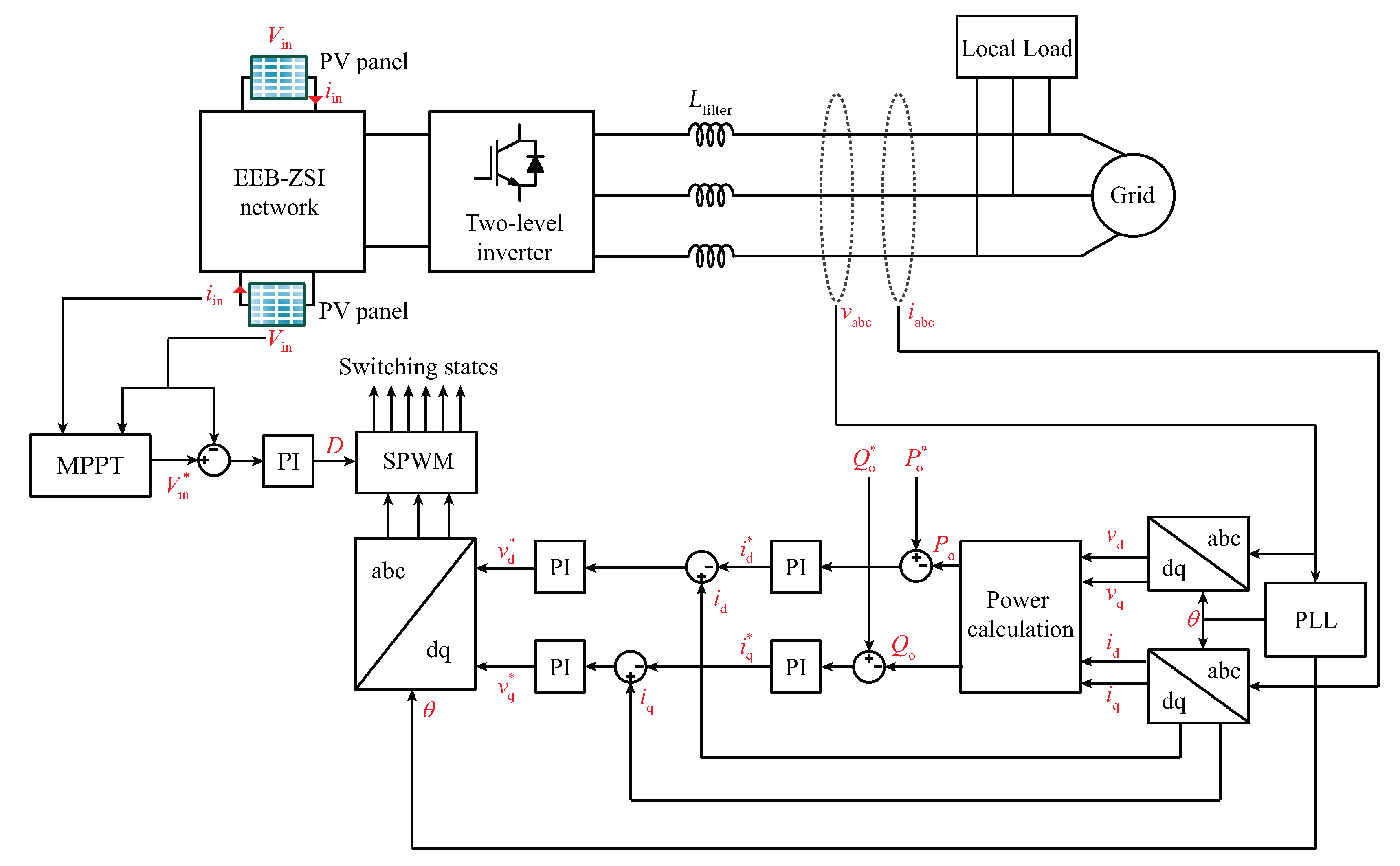
To implement the proposed EEB-ZSI in the PV systems, a basic control diagram is presented in Figure 6. As discussed in [27,28], the impedance source inverters can be controlled by adjusting duty cycle D and modulation index M. More specifically, in PV systems, the duty cycle can be used to achieve the maximum power point tracking (MPPT) of the PV panel; meanwhile, the modulation index is used to control the inverter output power. As shown in Figure 6, two separate PV panels have the same input voltage and current assuming that they operate under the same condition. By measuring and , the MPPT can be achieved to generate the required voltage signal [29]. Then, the duty cycle can be obtained from a proportional-integral (PI) controller. In addition, the control algorithm of the inverter side is similar to the conventional voltage source inverter. By transforming the grid/load side voltages and currents from the frame to the frame, the switching states can be determined according to the active power and reactive power closed-loop control based on the PI controllers [30].
3. Fault-Tolerant Analysis
Additionally, the fault-tolerant capability of the proposed EEB-ZSI under faulty modes is another important advantage in comparison to other topologies. Detailed analysis under open-circuit (OC), short-circuit (SC), and DC source unbalance conditions is performed in this section.
3.1. Open-Circuit Analysis
Figure 7a presents the schematic of the EEB-ZSI under the OC condition, where one DC source is open-circuited. Accordingly, Figure 7b,c presents the equivalent circuits in the ST and NST states. It can be seen that and (red part) are not used for power transfer due to their disconnection from the circuit. Moreover, is in conduction mode, and is in the OFF-state during these two operation states. Then, the following equations are derived:
3.2. Short-Circuit Analysis
When an SC fault happens for one DC source, EEB-ZSI can still operate, and the equivalent circuits are presented in Figure 8. In this condition, the operation is the same as that of the normal condition. However, only half of the power can be provided compared with the normal output power. Likewise, the peak DC-link voltage and voltage gain can be derived as:
Assuming that the input voltages from the two DC sources are identical in normal operation, the boost capability in the SC condition is reduced by half as opposed to the normal operation.
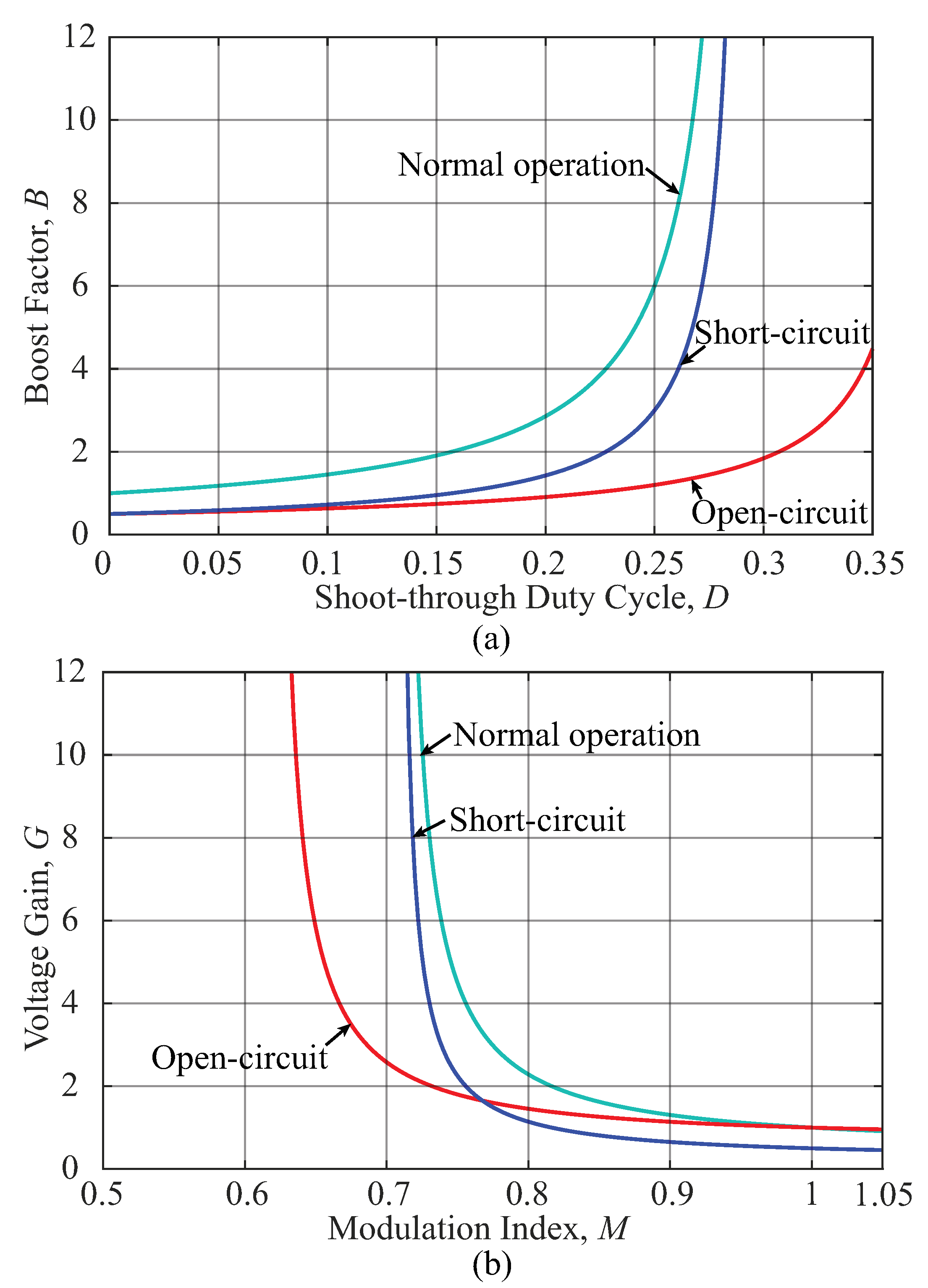
According to the above analysis, the boost factor and voltage gain for the EEB-ZSI are further outlined in Table 2, and the corresponding relationship is shown in Figure 9. For a fair comparison, the input DC voltages are the same. In contrast to the normal operation case with the same D and M, the boosting capability of EEB-ZSI is greatly reduced due to the OC and SC faults. Nevertheless, the fault-tolerant operation can be ensured by adjusting the duty cycle and modulation index. It is noted that M should be decreased to meet the requirements of the normal condition if the faults happen, which may lead to an unexpected power quality and efficiency reduction. Therefore, this paper only discusses that the system rides through the DC faults by regulating the DC input voltage.
3.3. Source-Unbalance Analysis
Considering the special scenario in PV systems, the DC voltages embedded in EEB-ZSI will be different when the shaded PV modules are bypassed by diodes. In this case, the currents generated by the PV panels remain the same (identical panels). Here, the two DC sources are denoted by and . Clearly, the operation principle remains the same compared with the normal operation condition. According to the above, the peak DC-link voltage is expressed as:
In contrast to Equation (19), although the equation to calculate the boost factor is not changed, the peak DC-link voltage is determined by the total voltage of the two sources. Therefore, the SC condition can be treated as a special source-unbalance case.
4. Experimental Verification
To confirm the effectiveness of EEB-ZSI under normal and faulty conditions, the prototype was built, and the experimental results are provided. The key parameters of the proposed EEB-ZSI in the experimental tests are shown in Table 3. Three cases were carried out to validate the feasibility of EEB-ZSI (i.e., normal operation and OC and SC (unbalance source) modes), and the M and D were selected as 0.85 and 0.15 in the initial state.
Case 1: Under the normal condition, the input voltages of the proposed EEB-ZSI were the same, and the experimental results are indicated in Figure 10.
According to Equation (20), B was 1.91, and the inverter output voltage and DC-link voltage were boosted to 153 V (the peak). Figure 10 shows the experimental results for the proposed EEB-ZSI under normal operation; the DC-link voltage was boosted from 80 to 150 V. The obtained experimental result in terms of output voltage was lower than the theoretical value considering the parasitics of the components. Moreover, kept a continuous output state, which verified the improvement in terms of the continuous input current.
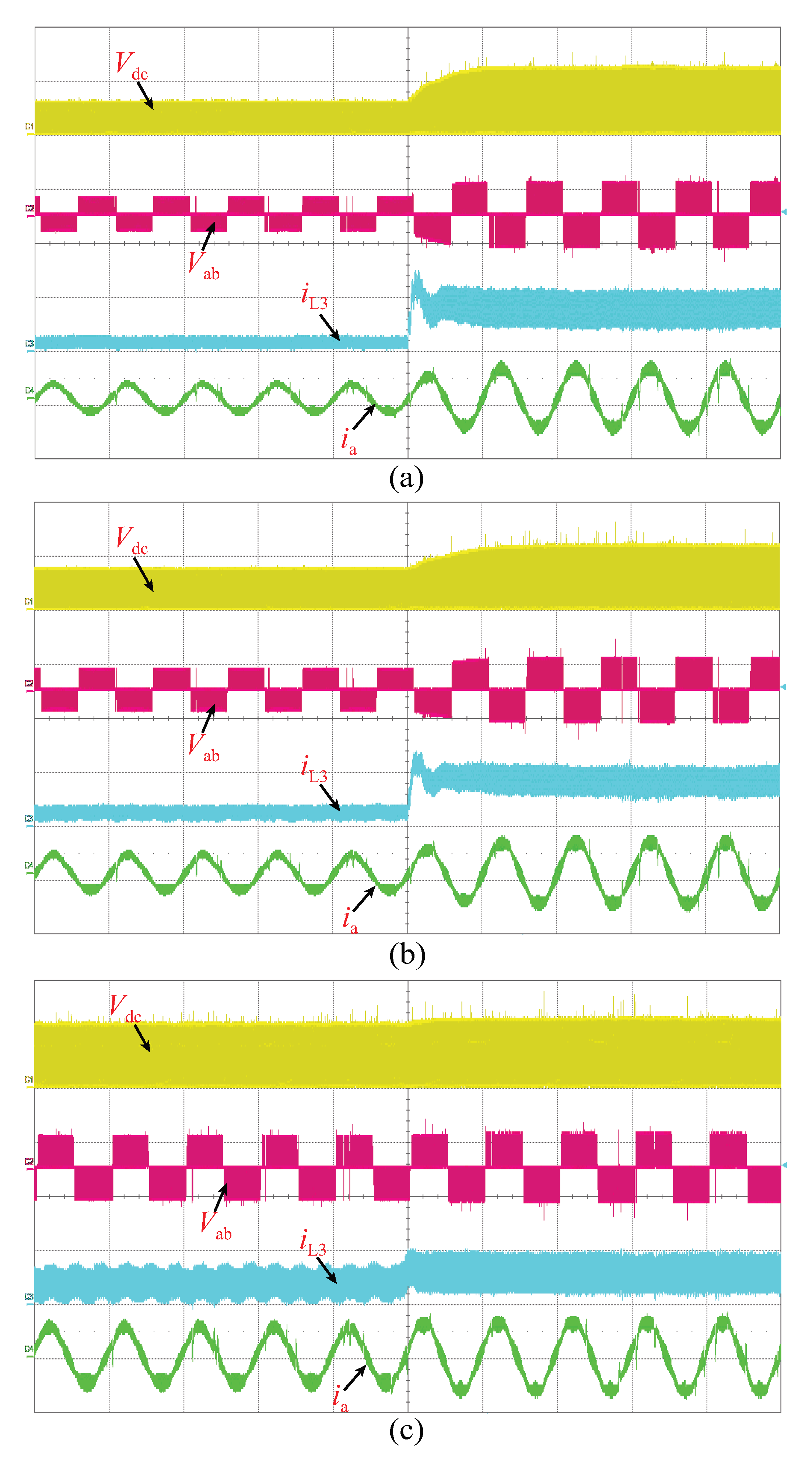
Case 2: When the EEB-ZSI operated under the OC condition, the experimental results were as presented in Figure 11a. When M and D were in the initial state, the DC-link voltage was boosted to 60 V based on Equation (34), which matched with the results in Figure 11b. To further compensate the decreased voltage under the OC condition, M and D could be adjusted to one and 0.305 based on the previous analysis. Moreover, it is clear in Figure 11a that the DC-link voltage and output voltage increased to the required value. Meanwhile, the output power increased with the increase of the input current (), and the load current also increased compared to the initial state.
Case 3: This case was carried out under the SC (unbalanced source) condition. Compared to the normal operation condition, the power was only supplied by one DC source. Therefore, the peak DC-link voltage was boosted to 75 V in the initial state, which was half of the boosted voltage in normal operation. After modulating M and D to one and 0.219, the required voltage level could be ensured, as shown in Figure 11b. In addition, in terms of unbalanced source conditions, two DC sources provided unbalanced power with two DC sources being 40 V and 20 V, respectively. According to Equation (36), the boosted voltage was calculated to be 114 V, which was three-quarters of the boosted voltage in normal operation. Similarly, by changing M and D to one and 0.172, the boosted voltage was restored to the normal level, as shown in Figure 11c.
5. Conclusions
In this paper, an embedded enhanced-boost Z-source inverter (EEB-ZSI) with continuous input current and fault-tolerant capabilities was proposed. The operation principles were presented in detail, where the proposed topology was also compared with the prior-art solutions. Compared to the traditional embedded ZSIs and the enhanced-boost ZSI (EB-ZSI), the EEB-ZSI could realize continuous input currents, while also maintaining a high conversion ratio. Additionally, the proposed EEB-ZSI could tolerate the DC source faults with a relatively large boost ratio, where it could improve the system continuity of operation. Extensive experimental tests also confirmed the claim that the proposed EEB-ZSI was a promising impedance-source converter in terms of continuous input current, high boosting ratio, and strong fault-tolerant capability.
Author Contributions
Conceptualization, J.Y., and Y.Y.; formal analysis, J.Y.; software, J.Y.; validation, J.Y.; writing, review and editing, J.Y., Y.Y., P.L., Y.S., and F.B. All authors read and agreed to the published version of the manuscript.
Funding
This research was funded by Reliable Power Electronic based Power Systems (REPEPS) by THE VELUX FOUNDATIONS (Award Ref. No. 00016591).
Conflicts of Interest
The authors declare no conflict of interest.
References
- Liu, Y.; Abu-Rub, H.; Ge, B.; Blaabjerg, F.; Ellabban, O.; Loh, P.C. Impedance Source Power Electronic Converters; John Wiley & Sons: Hoboken, NJ, USA, 2016. [Google Scholar]
- Yang, Y.; Kim, K.A.; Blaabjerg, F.; Sangwongwanich, A. Advances in Grid-Connected Photovoltaic Power Conversion Systems; Woodhead Publishing: Cambridge, UK, 2018. [Google Scholar]
- Yuan, J.; Yang, Y.; Liu, P.; Shen, Y.; Qiu, Z.; Blaabjerg, F. An embedded enhanced-boost Z-source inverter. In Proceedings of the IEEE PEAC, Shenzhen, China, 4–7 November 2018; pp. 1–6. [Google Scholar]
- Yuan, J.; Yang, Y.; Blaabjerg, F. A switched quasi-Z-Source inverter with continuous input currents. Energies 2020, 13, 1390. [Google Scholar] [CrossRef] [Green Version]
- Yuan, J.; Mostaan, A.; Yang, Y.; Siwakoti, Y.P.; Blaabjerg, F. A modified Y-Source DC/DC converter with high voltage-gains and low switch stresses. IEEE Trans. Power Electron. 2020, 35, 7716–7720. [Google Scholar] [CrossRef]
- Mostaan, A.; Yuan, J.; Siwakoti, Y.P.; Esmaeili, S.; Blaabjerg, F. A trans-Inverse coupled-inductor semi-SEPIC DC/DC converter with full control range. IEEE Trans. Power Electron. 2019, 34, 10398–10402. [Google Scholar] [CrossRef]
- Singh, S.A.; Carli, G.; Azeez, N.A.; Williamson, S.S. Modeling, design, control, and implementation of a modified Z-source integrated PV/Grid/EV DC charger/inverter. IEEE Trans. Ind. Electron. 2018, 65, 5213–5220. [Google Scholar] [CrossRef]
- Peng, F.Z. Z-source inverter. IEEE Trans. Ind. Appl. 2003, 39, 504–510. [Google Scholar] [CrossRef]
- Abdelhakim, A.; Blaabjerg, F.; Mattavelli, P. Modulation schemes of the three-phase impedance source inverters part I: Classification and review. IEEE Trans. Ind. Electron. 2018, 65, 6309–6320. [Google Scholar] [CrossRef]
- Anderson, J.; Peng, F.Z. Four quasi-Z-Source inverters. In Proceedings of the IEEE Power Electronics Specialists Conference, Rhodes, Greece, 15–19 June 2008; pp. 2743–2749. [Google Scholar]
- Zhu, M.; Yu, K.; Luo, F.L. Switched inductor Z-Source inverter. IEEE Trans. Power Electron. 2010, 25, 2150–2158. [Google Scholar]
- Li, D.; Loh, P.C.; Zhu, M.; Gao, F.; Blaabjerg, F. Generalized multicell switched-inductor and switched-capacitor Z-Source inverters. IEEE Trans. Power Electron. 2013, 28, 837–848. [Google Scholar] [CrossRef]
- Nguyen, M.; Lim, Y.; Cho, G. Switched-inductor quasi-Z-source inverter. IEEE Trans. Power Electron. 2011, 26, 3183–3191. [Google Scholar] [CrossRef]
- Gajanayake, C.J.; Gooi, H.B.; Luo, F.L.; So, P.L.; Siow, L.K.; Vo, Q.N. Simple modulation and control method for new extended boost quasi Z-source. In Proceedings of the TENCON Conference, Singapore, 23–26 January 2009; pp. 1–6. [Google Scholar]
- Gajanayake, C.J.; Luo, F.L.; Gooi, H.B.; So, P.L.; Siow, L.K. Extended-boost Z-source inverters. IEEE Trans. Power Electron. 2010, 25, 2642–2652. [Google Scholar] [CrossRef]
- Fathi, H.; Madadi, H. Enhanced-boost Z-source inverters with switched Z-impedance. IEEE Trans. Ind. Electron. 2015, 62, 7569–7577. [Google Scholar] [CrossRef]
- Mazumder, S.K.; Burra, R.K.; Acharya, K. A ripple-mitigating and energy-efficient fuel cell power-conditioning system. IEEE Trans. Power Electron. 2006, 22, 1437–1452. [Google Scholar] [CrossRef]
- Khateb, A.E.; Rahim, N.A.; Selvaraj, J.; Williams, B.W. The effect of input current ripple on the photovoltaic panel efficiency. In Proceedings of the IEEE CEAT, Lankgkawi, Malaysia, 18–20 November 2013; pp. 478–481. [Google Scholar]
- Jagan, V.; Kotturu, J.; Das, S. Enhanced-boost quasi-Z-source inverters with two-switched impedance networks. IEEE Trans. Ind. Electron. 2017, 64, 6885–6897. [Google Scholar] [CrossRef]
- Loh, P.C.; Gao, F.; Blaabjerg, F. Embedded EZ-source inverters. IEEE Trans. Ind. Appl. 2010, 46, 256–267. [Google Scholar]
- Babaei, E.; Asl, E.S.; Babayi, M.H.; Laali, S. Developed embedded switched-Z-source inverter. IET Power Electron. 2016, 9, 1828–1841. [Google Scholar] [CrossRef]
- Gao, F.; Loh, P.C.; Li, D.; Blaabjerg, F. Asymmetrical and symmetrical embedded Z-source inverters. IET Power Electron. 2011, 4, 181–193. [Google Scholar] [CrossRef]
- Pires, V.F.; Cordeiro, A.; Foito, D.; Martins, J.F. Quasi-Z-source inverter with a T-type converter in normal and failure mode. IEEE Trans. Power Electron. 2016, 31, 7462–7470. [Google Scholar] [CrossRef]
- Pires, V.F.; Foito, D.; Cordeiro, A. Three-phase qZ-source inverter with fault tolerant capability. IET Power Electron. 2017, 10, 1852–1858. [Google Scholar] [CrossRef]
- Sivakumar, K. A fault-tolerant single-phase five-level inverter for grid-independent PV systems. IEEE Trans. Ind. Electron. 2015, 62, 7569–7577. [Google Scholar]
- Shen, M.; Wang, J.; Joseph, A.; Peng, F.Z.; Tolbert, L.M.; Adams, D.J. Constant boost control of the Z-source inverter to minimize current ripple and voltage stress. IEEE Trans. Ind. Appl. 2006, 42, 770–778. [Google Scholar] [CrossRef]
- Huang, Y.; Shen, M.; Peng, F.Z.; Wang, J. Z-Source Inverter for Residential Photovoltaic Systems. IEEE Trans. Power Electron. 2006, 21, 1776–1782. [Google Scholar] [CrossRef]
- Siwakoti, Y.P.; Peng, F.Z.; Blaabjerg, F.; Loh, P.C.; Town, G.E.; Yang, S. Impedance-Source Networks for Electric Power Conversion Part II: Review of Control and Modulation Techniques. IEEE Trans. Power Electron. 2015, 30, 1887–1906. [Google Scholar] [CrossRef]
- Subudhi, B.; Pradhan, R. A Comparative Study on Maximum Power Point Tracking Techniques for Photovoltaic Power Systems. IEEE Trans. Sustain. Energy 2013, 4, 89–98. [Google Scholar] [CrossRef]
- Ge, B.; Abu-Rub, H.; Peng, F.Z.; Lei, Q.; de Almeida, A.T.; Ferreira, F.J.T.E.; Sun, D.; Liu, Y. An Energy-Stored Quasi-Z-Source Inverter for Application to Photovoltaic Power System. IEEE Trans. Ind. Electron. 2013, 60, 4468–4481. [Google Scholar] [CrossRef]
Figure 1.
Two impedance networks feeding a conventional two level three phase inverter: (a) Z-source network [8] and (b) enhanced-boost Z-source network [16]. Here, is the input voltage, and D, C, and L with subscripts represent diodes, capacitors, and inductors in the impedance network.
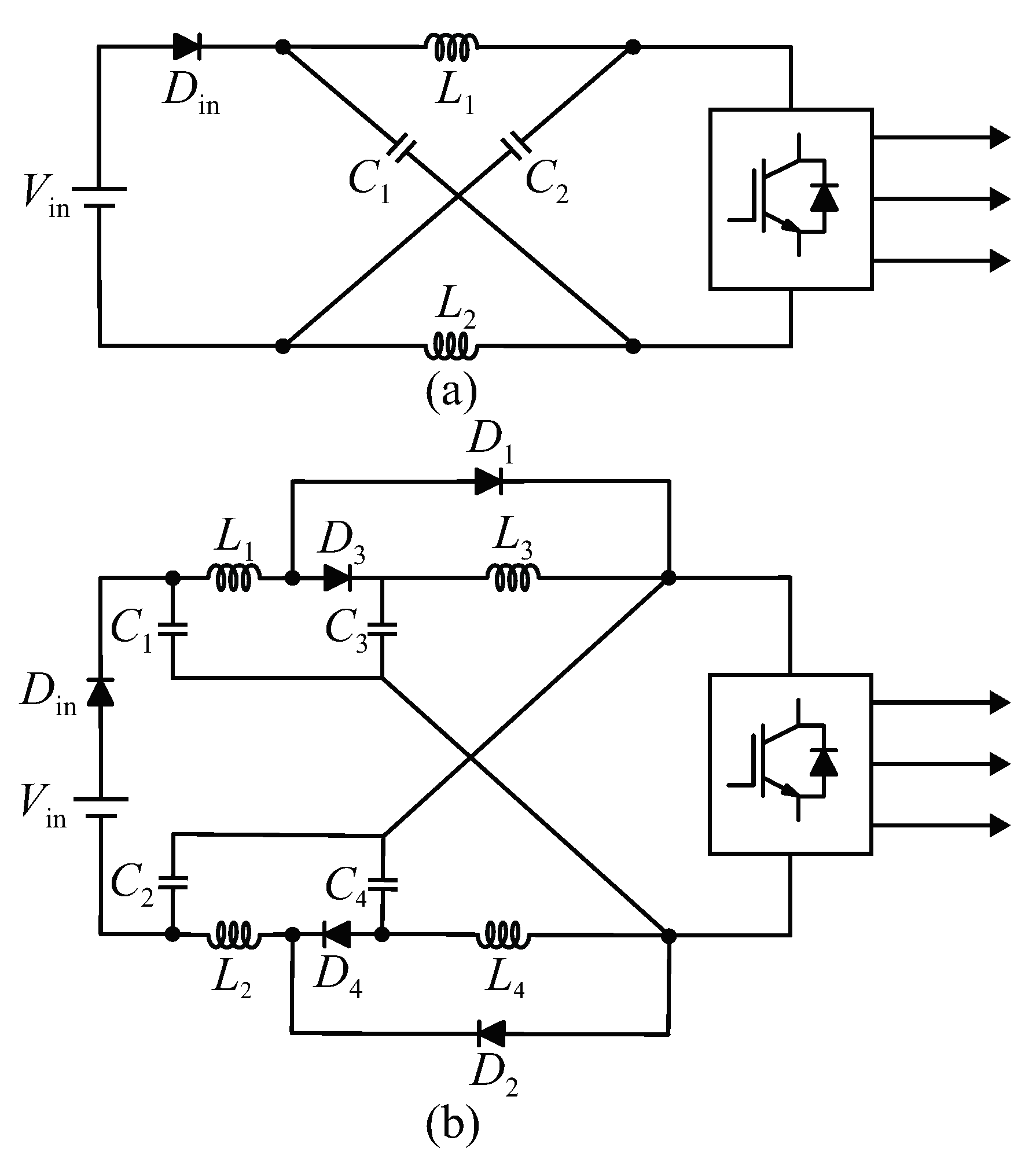
Figure 2.
Example of an embedded Z-source inverter, where two identical DC sources are connected in series with the inductors of the Z-source network shown in Figure 1a [20].
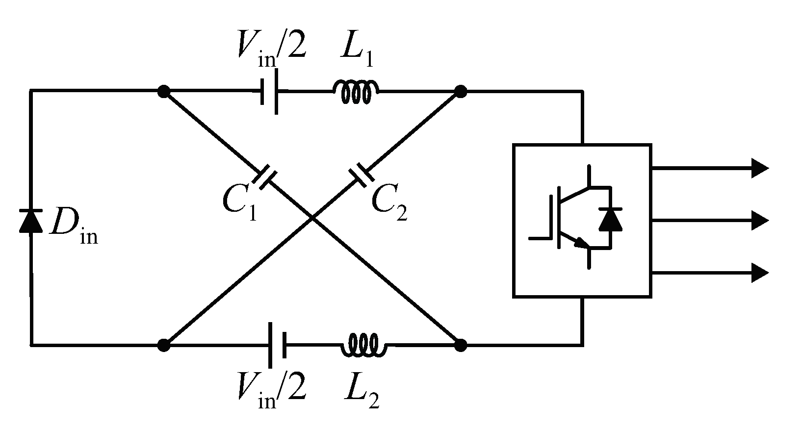
Figure 3.
Proposed embedded enhanced-boost Z-source inverter (EEB-ZSI) topology: (a) entire circuit diagram, (b) equivalent circuit during the shoot-through state, and (c) equivalent circuit during the non-shoot-through state.
Figure 3.
Proposed embedded enhanced-boost Z-source inverter (EEB-ZSI) topology: (a) entire circuit diagram, (b) equivalent circuit during the shoot-through state, and (c) equivalent circuit during the non-shoot-through state.
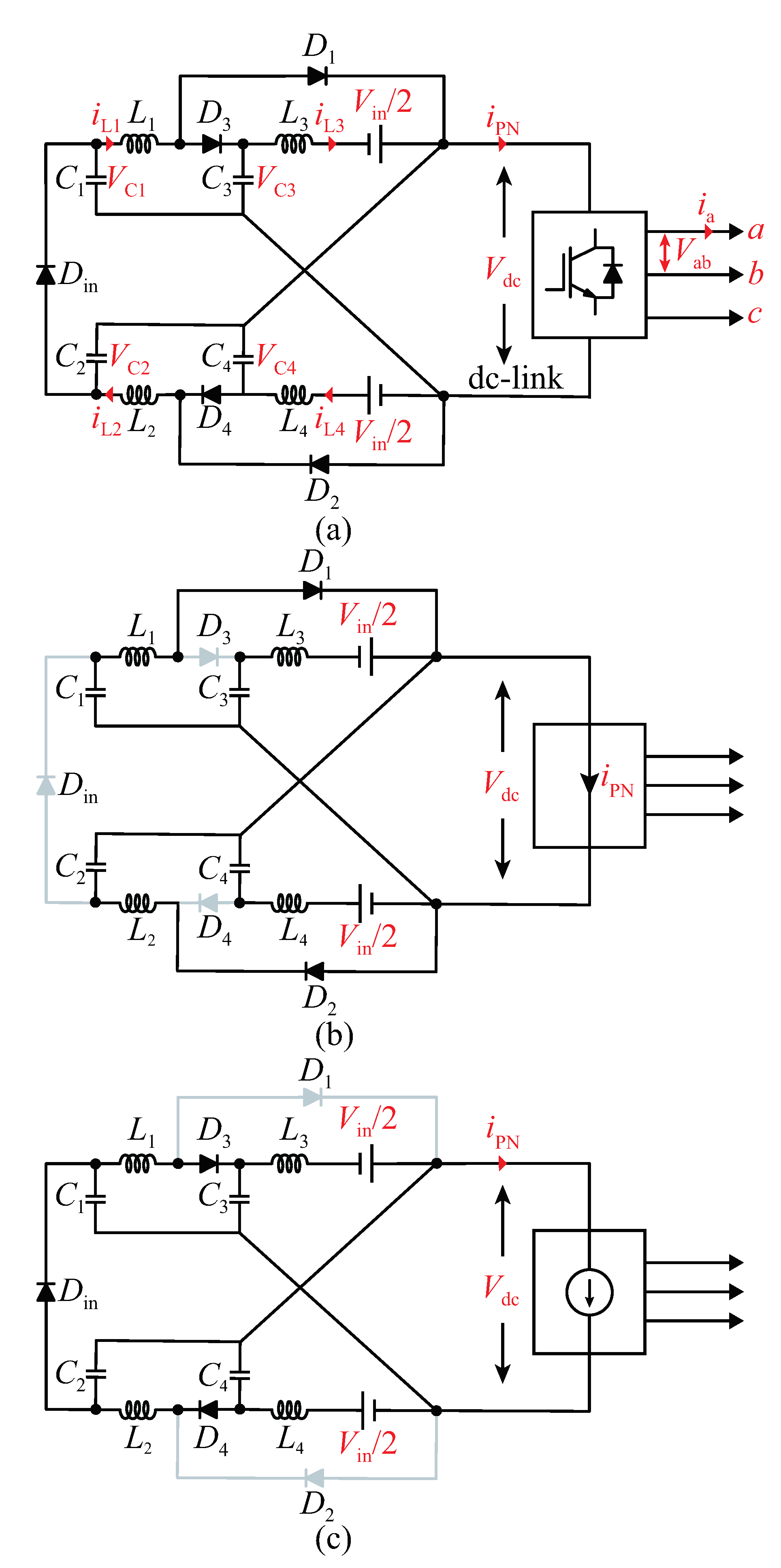
Figure 4.
Comparison of the selected Z-source networks: (a) boost factor versus the shoot-through duty-ratio D and (b) voltage gain versus the modulation index M (ZSI [8], embedded-ZSI (E-ZSI) [20], diode-assisted ZSI (DA-ZSI) [15], switched-inductor ZSI (SI-ZSI) [11], and EB-ZSI [16]).
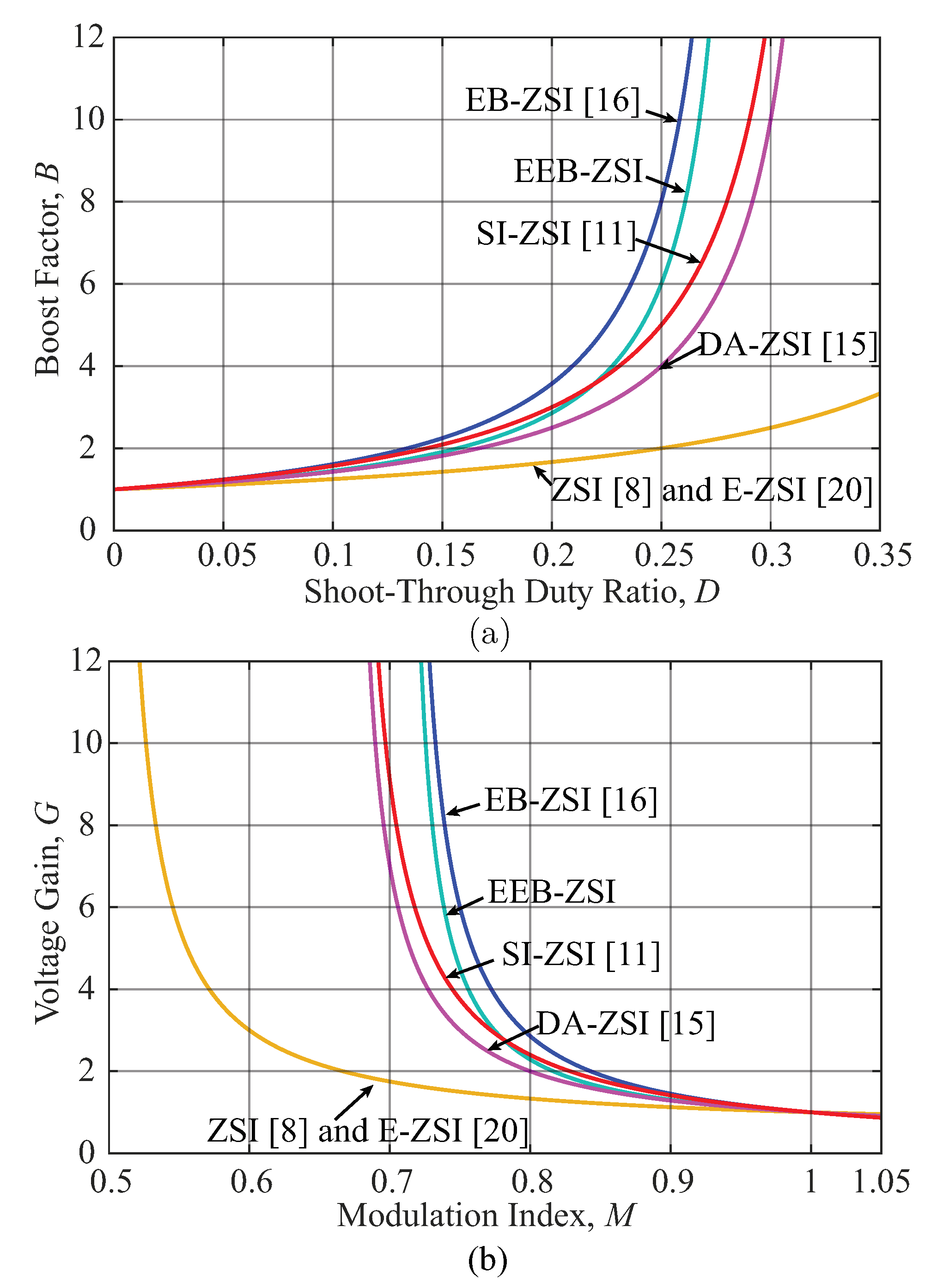
Figure 5.
Comparison of the selected Z-source networks: (a) normalized voltage stress on the power switches and (b) normalized capacitor voltage stress of the EB-ZSI and the proposed EEB-ZSI.
Figure 5.
Comparison of the selected Z-source networks: (a) normalized voltage stress on the power switches and (b) normalized capacitor voltage stress of the EB-ZSI and the proposed EEB-ZSI.
Figure 6.
General control diagram for an EEB-ZSI-based PV system. (, , , and represent the actual/required active power and the actual/required reactive power; , , , and are the actual/required d-axis current components and the q-axis current components; , , , and are the actual/required d-axis voltage components and the q-axis voltage components; is the actual three-phase voltage signals; are the actual three-phase currents; is the phase angle from the phase locked loop (PLL)).

Figure 7.
Circuit diagrams of the proposed EEB-ZSI under the open-circuit (a DC source) condition: (a) system schematic, (b) equivalent circuit diagram during the shoot-through state, and (c) equivalent circuit diagram during the non-shoot-through state.
Figure 7.
Circuit diagrams of the proposed EEB-ZSI under the open-circuit (a DC source) condition: (a) system schematic, (b) equivalent circuit diagram during the shoot-through state, and (c) equivalent circuit diagram during the non-shoot-through state.
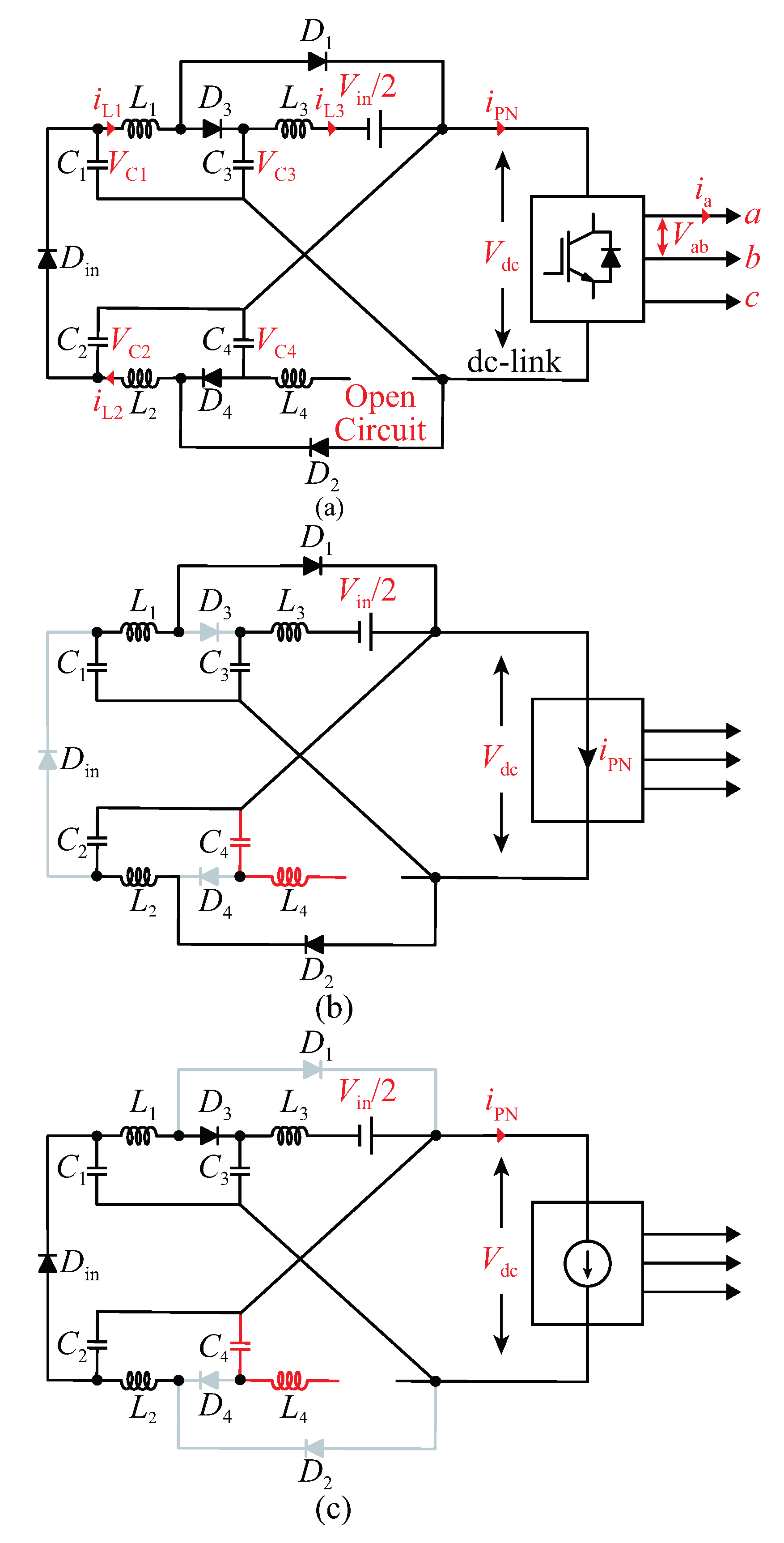
Figure 8.
Circuit diagrams of the proposed EEB-ZSI under the short-circuit (a DC source) condition: (a) system diagram, (b) equivalent circuit diagram during the shoot-through state, and (c) equivalent circuit diagram during the non-shoot-through state.
Figure 8.
Circuit diagrams of the proposed EEB-ZSI under the short-circuit (a DC source) condition: (a) system diagram, (b) equivalent circuit diagram during the shoot-through state, and (c) equivalent circuit diagram during the non-shoot-through state.

Figure 9.
Comparison under normal and fault conditions: (a) boost factor comparison and (b) voltage gain comparison.
Figure 9.
Comparison under normal and fault conditions: (a) boost factor comparison and (b) voltage gain comparison.

Figure 10.
Experimental results of the proposed EEB-ZSI under normal operation. ( (100 V/div), (200 V/div), (5 A/div), (2 A/div), time (20 ms/div)).
Figure 10.
Experimental results of the proposed EEB-ZSI under normal operation. ( (100 V/div), (200 V/div), (5 A/div), (2 A/div), time (20 ms/div)).
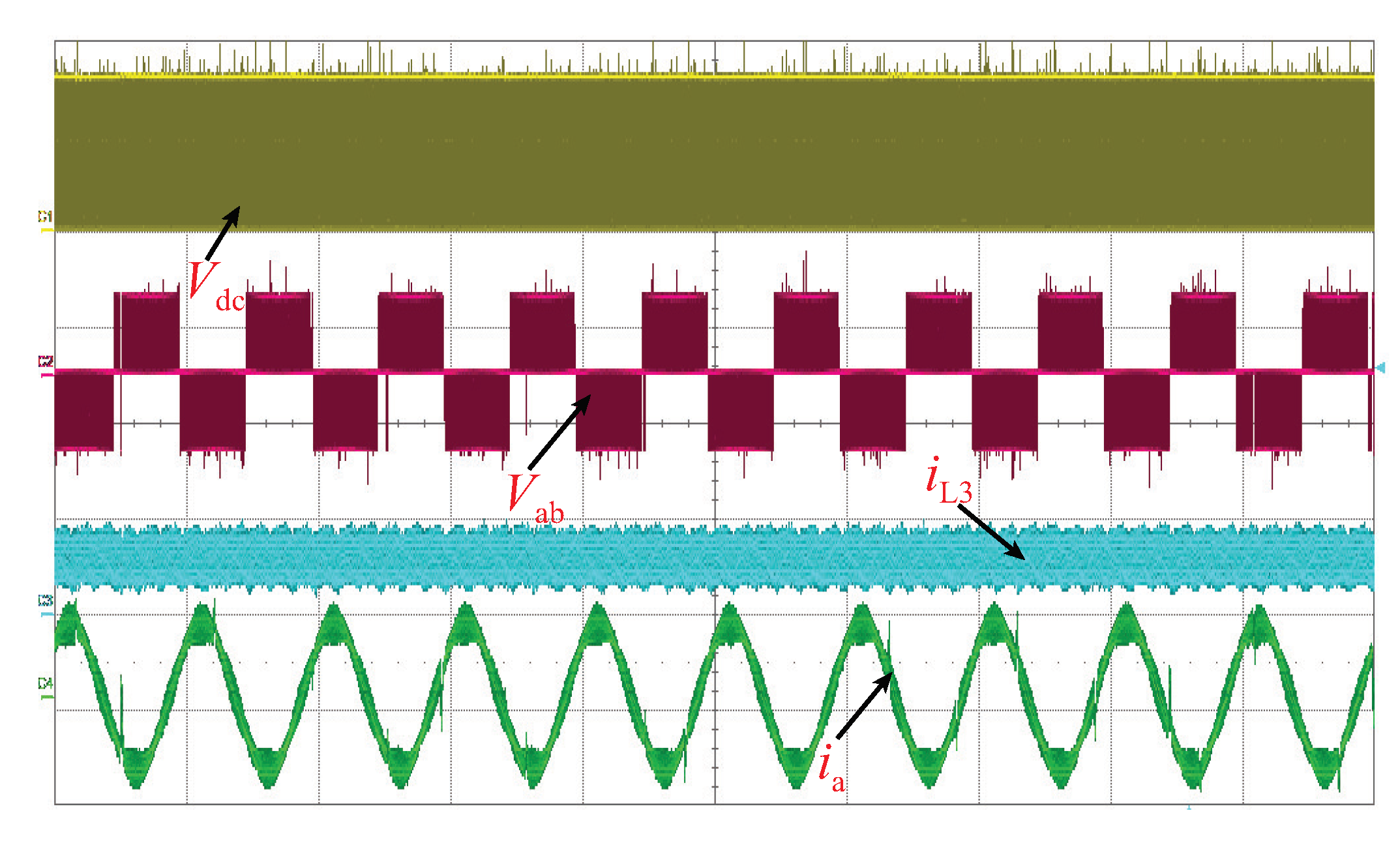
Figure 11.
Experimental results of the proposed EEB-ZSI under abnormal conditions: (a) open-circuit (OC) condition, (b) short-circuit (SC) condition, and (c) unbalanced-source condition ( (100 V/div), (200 V/div), (5 A/div), (2 A/div), time (20 ms/div)).
Figure 11.
Experimental results of the proposed EEB-ZSI under abnormal conditions: (a) open-circuit (OC) condition, (b) short-circuit (SC) condition, and (c) unbalanced-source condition ( (100 V/div), (200 V/div), (5 A/div), (2 A/div), time (20 ms/div)).

Table 1.
Benchmarking of selected impedance source inverters.
| Symbol | ZSI [8] | E-ZSI [20] | DA-ZSI [16] | SI-ZSI [16] | EB-ZSI [16] | EEB-ZSI | |
|---|---|---|---|---|---|---|---|
| Boost Factor | B | ||||||
| Voltage Gain | G | ||||||
| Switch Stress | |||||||
| , Stress | NA | NA | NA | NA | |||
| , Stress | NA | NA | NA | NA | 1 |
Table 2.
Comparisons of the proposed EEB-ZSI under normal and fault conditions.
| Normal Condition | Open-Circuit Condition | Short-Circuit Condition | |
|---|---|---|---|
| B | |||
Table 3.
Parameters of EEB-ZSI.
| Parameter | Symbol | Value |
|---|---|---|
| DC input voltage | V | |
| EEB-ZSI inductance | H | |
| EEB-ZSI capacitor | F | |
| Load inductance | mH | |
| Load resistance | ||
| Switching frequency | 5 kHz |
© 2020 by the authors. Licensee MDPI, Basel, Switzerland. This article is an open access article distributed under the terms and conditions of the Creative Commons Attribution (CC BY) license (http://creativecommons.org/licenses/by/4.0/).
Share and Cite
MDPI and ACS Style
Yuan, J.; Yang, Y.; Liu, P.; Shen, Y.; Blaabjerg, F. Modified Impedance-Source Inverter with Continuous Input Currents and Fault-Tolerant Operations. Energies 2020, 13, 3408. https://doi.org/10.3390/en13133408
AMA Style
Yuan J, Yang Y, Liu P, Shen Y, Blaabjerg F. Modified Impedance-Source Inverter with Continuous Input Currents and Fault-Tolerant Operations. Energies. 2020; 13(13):3408. https://doi.org/10.3390/en13133408
Chicago/Turabian StyleYuan, Jing, Yongheng Yang, Ping Liu, Yanfeng Shen, and Frede Blaabjerg. 2020. "Modified Impedance-Source Inverter with Continuous Input Currents and Fault-Tolerant Operations" Energies 13, no. 13: 3408. https://doi.org/10.3390/en13133408
Note that from the first issue of 2016, this journal uses article numbers instead of page numbers. See further details here.