1. Introduction
Energy is considered as necessary support in modern technological and industrial progress [
1,
2]. Among multiple attempts that aim at optimizing the energy efficiency and developing new energy, much attention of researchers has been given to distributed power generation technology and its application in a micro-grid.
Distributed power generation [
3] is a small-scale power generation built near power users and relies on scattered energy for power generation, with its output ranging from several kilowatts to hundreds of megawatts. The distributed power system consists of two parts: distributed generation power supply and distributed power supply. The former focuses on the production of electrical energy, while the latter emphasizes the transmission of electrical energy. Compared with the Centralized Power System (CPS), the distributed power system is a modular high-power supply system that connects several small and medium-sized power supply modules in parallel [
4,
5] and is widely used in aerospace power supply, power system, new energy vehicles, etc. Meanwhile, as an important component of smart grid, a distributed power system contains a variety of power electronic equipment [
6]. With the development of smart grids, distributed power systems integrate communication technology, sensor measurement technology, and information technology to meet the needs of power generation, grid operation, and terminal power consumption [
7]. The distributed power supply and communication technology are introduced into the smart grid to achieve the real-time information exchange and the supply balance at the device level and to establish a highly automated energy exchange network with bidirectional flow of power and information [
8].
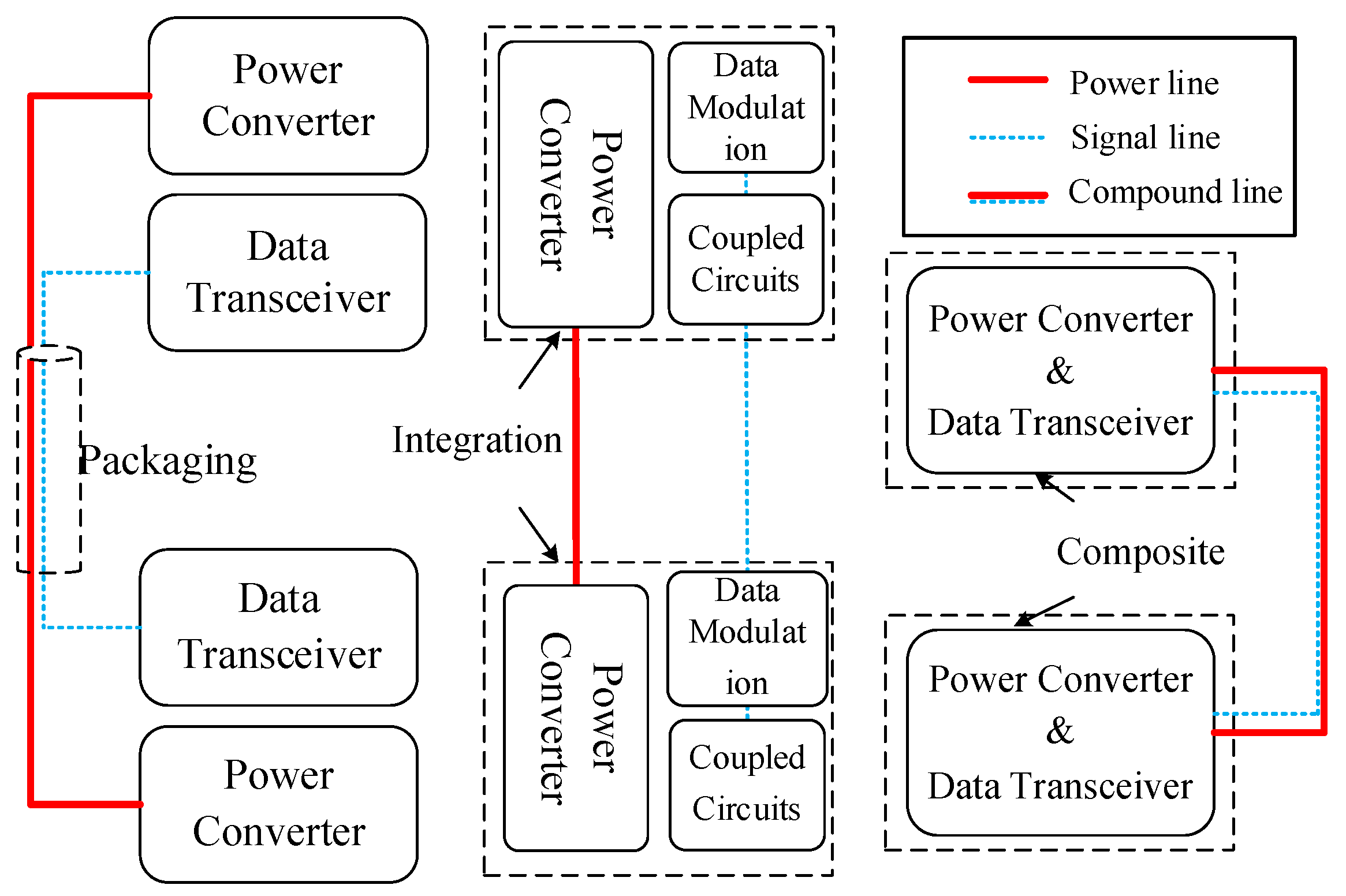
Figure 1 shows the structure of a distributed power system.
In the traditional distributed power system, an additional communication circuit is introduced to the power circuit to receive control commands or exchange data between power converters. For example, Controller Area Network (CAN), Recommended Standard-485 (RS-485), and other wired communication technologies [
9] are widely used in distributed power systems. However, the system becomes more complex and its installation cost increases with additional communication circuits. As in wireless transmissions such as WiMAX, Wi-Fi and Zigbee with no hardware lines, their independent signal transmission devices also need be optimized for their reliability and adaptability to environment.
In order to simplify the communication system of the power grid and to reduce the communication cost, recent research focuses on Power over Ethernet (PoE), a new communication technology that can combine two types of communication and power systems. The compound communication technology of energy signals has gone through three developmental stages as encapsulation, integration, and fusion. The schematic diagram is shown in
Figure 2.
At present, the compound communication technology is divided into three categories: (1) using the existing power line for signal modulation, such as power line communication (PLC); (2) using independent communication lines, such as the bus power supply method in the IEC61158-2 standard; and (3) adding power supply devices to existing communication lines. The power line communication technology has become a research focus since it was proposed in the 1920s, for it has the advantages of simple networking, wide distribution, no need for rewiring, and convenient operation [
10,
11]. The principle of PLC uses power lines of various voltage levels as media for voice or data transmission. It has been widely applied in various areas such as automatic electricity meter reading, power supply management, and grid load control [
12,
13].
Recent decades have witnessed progresses in power line communication. In [
14], the author proposed a new DC-bus PLC system powered by a synchronous switching converter. Implementation of the PLC technology is simple and only requires proper modulation of the controllable switching devices in the converter. The research in [
15] studied the application of PLC technology in the distributed digitally controlled DC-DC converters. A small duty-cycle perturbation at half of switching frequency is introduced to enhance the signal of low power transmission. An enhanced PLC strategy using switching frequency modulation is proposed in [
16] to optimize the power converter by improving the reliability of DC microgrids operation. The literature of [
17] proposes a solution that only uses the signal during the switching phase. However, such a proposal still has many limitations due to the high frequency content of the signal and the possible attenuation on the power line. In [
18], the frequency and duty-cycle modulation methods are mainly discussed. By modulating the duty-cycle of the PWM signal at the half of switching frequency, the researcher introduces perturbation to the common supply bus voltage, which increases the transmission within the bus bandwidth and ensures the distance and accuracy of the signal transmission. Researchers in [
19] also proposed a compound modulation method for electrical energy signals, using the intrinsic ripple initiated in switch mode power supplies as signal carriers to implement a narrow-frequency PLC in a distributed DC source system. The above researches on energy and signal compound transmission are all conducted on DC/DC converter circuit.
Switched Reluctance Drive (SRD), with its simple structure, reliable operation, and low cost, is used as the core part of a new speed control system. It can perform DC speed regulation and AC speed regulation and has been used in fans, compressors, traction locomotives, electric vehicles, aircraft, and other occasions [
20]. Recently, a new modulation and demodulation strategy to DC power-line data transmission for Switched Reluctance Generator (SRG) integrated microgrid is proposed, of which the turn-on and turn-off angle are adopted to regulate the voltage ripple for carrying data [
21]. In [
22], a soft-PWM method to power/signal synchronous transmission for SRG based DC microgrids is presented. The switches are modulated to produce voltage ripples with specific frequency for data transmission. However, these is no article to discuss the possibility of power and signal synchronous transmission in SRD system. In order to reduce the impact of signal modulation on the operation of SRD as well as to improve the communication rate and the efficiency, this paper proposes a frequency shift keying (FSK) modulation method in the Free-wheeling (FW) section for complex transmission of energy signals. The proposed method separates the upper and lower transistors of the SRD power converter in the excitation section for speed control. The soft chopping method is used, and the FSK modulation signal is adopted in the freewheeling section to drive the lower transistors. Therefore, the corresponding switching ripple is superimposed on the bus. At the receiving end of the bus, the Fourier iterative algorithm is used to simplify the calculation and to demodulate the signal more efficiently. Simulations are modeled to verify the effectiveness of the proposed method.
2. Compound Modulation Strategy of FSK Energy Signal
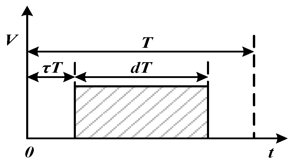
Pulse width modulation (PWM) theory has been widely used for controlling power electronic circuits. The typical PWM waveform is shown in
Figure 3, where
T is the period,
d is the duty cycle,
τT is the turn-on delay, and ω = 2π/T.
Fourier series expansion of PWM waveform can be obtained by
Assuming
ancos
nωt + bnsin
nωt = cncos(
nωt +
φn), Equation (1) can be simplified as
Note that c0 is truly equal to a0, by referring to (1) and (6).
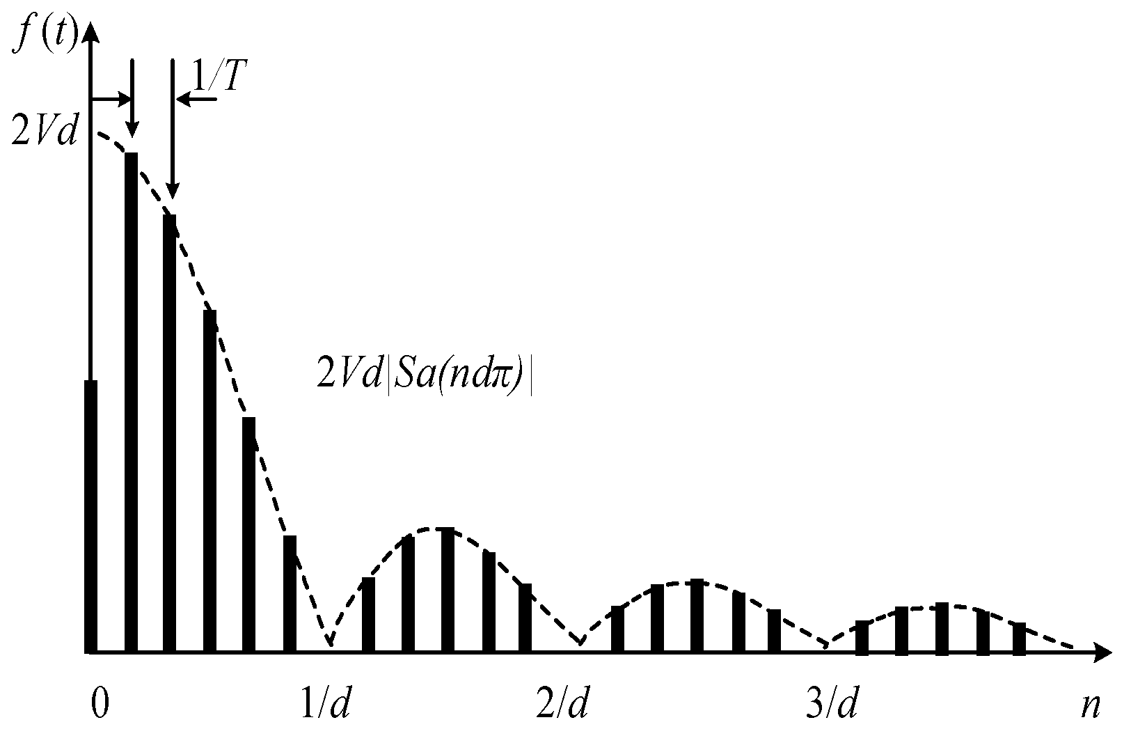
As shown in
Figure 4, the amplitude of the DC component is half of the corresponding value of the envelope 2
Vd|
Sa(
ndπ)|at the zero point. The discrete amplitude terms of the fundamental wave and each harmonic are function values at each integer point when
n is increased from 1 to infinite. The spacing between two adjacent spectral lines is 1/
T, indicating that each spectral line is located at an integer multiple of the fundamental frequency
f = 1/
T and that the spectral line at 1/
d and its integer multiple are 0.
It can be seen from Equation (5) and
Figure 4 that changing
f and
φ will not affect the DC component. Therefore,
f and
φ are relatively independent from
d, indicating that the signal can be modulated by changing these two variables. Using the switching harmonic components generated at the input and output of the converter as the signal carrier, the frequency
f or phase
φ of the switching signal is adjusted by the data signal in correspondence with two basic methods of digital modulation of the switching ripple, i.e., the frequency shift keying (FSK) modulation and phase shift keying (PSK) modulation, respectively. FSK-based composite modulation means using the FSK method to modulate the transmitted signal as well as PWM to achieve power line communication.
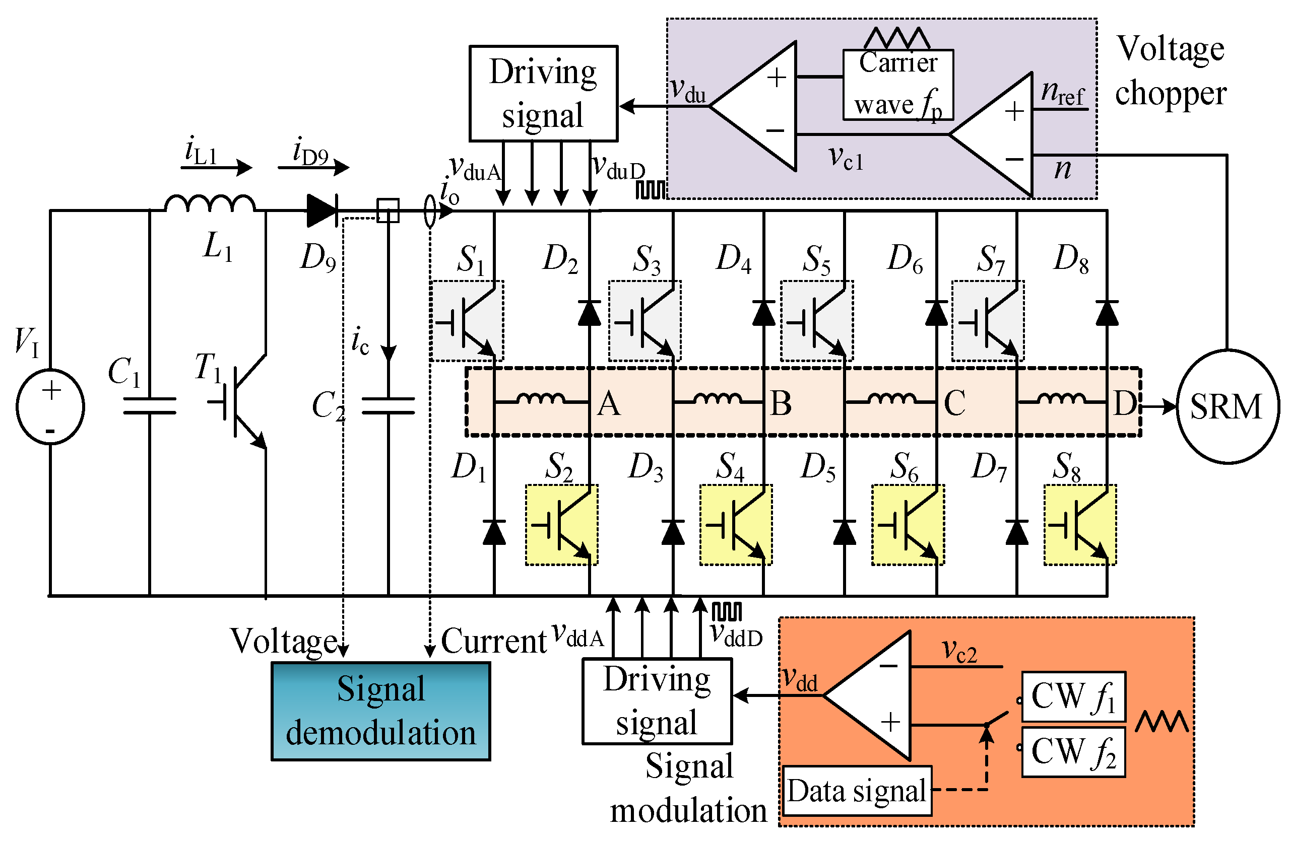
This paper adopts the FSK modulation signal in the freewheeling section of the lower transistors of the SRD power circuit. When the signal is “0”, the switching frequency of the circuit is f0; when the signal is “1”, the switching frequency is set to f1. Meanwhile, the PWM method is adopted to control the upper transistors of SRD power circuit.
3. Freewheeling Section Topology and Carrier Frequency Analysis
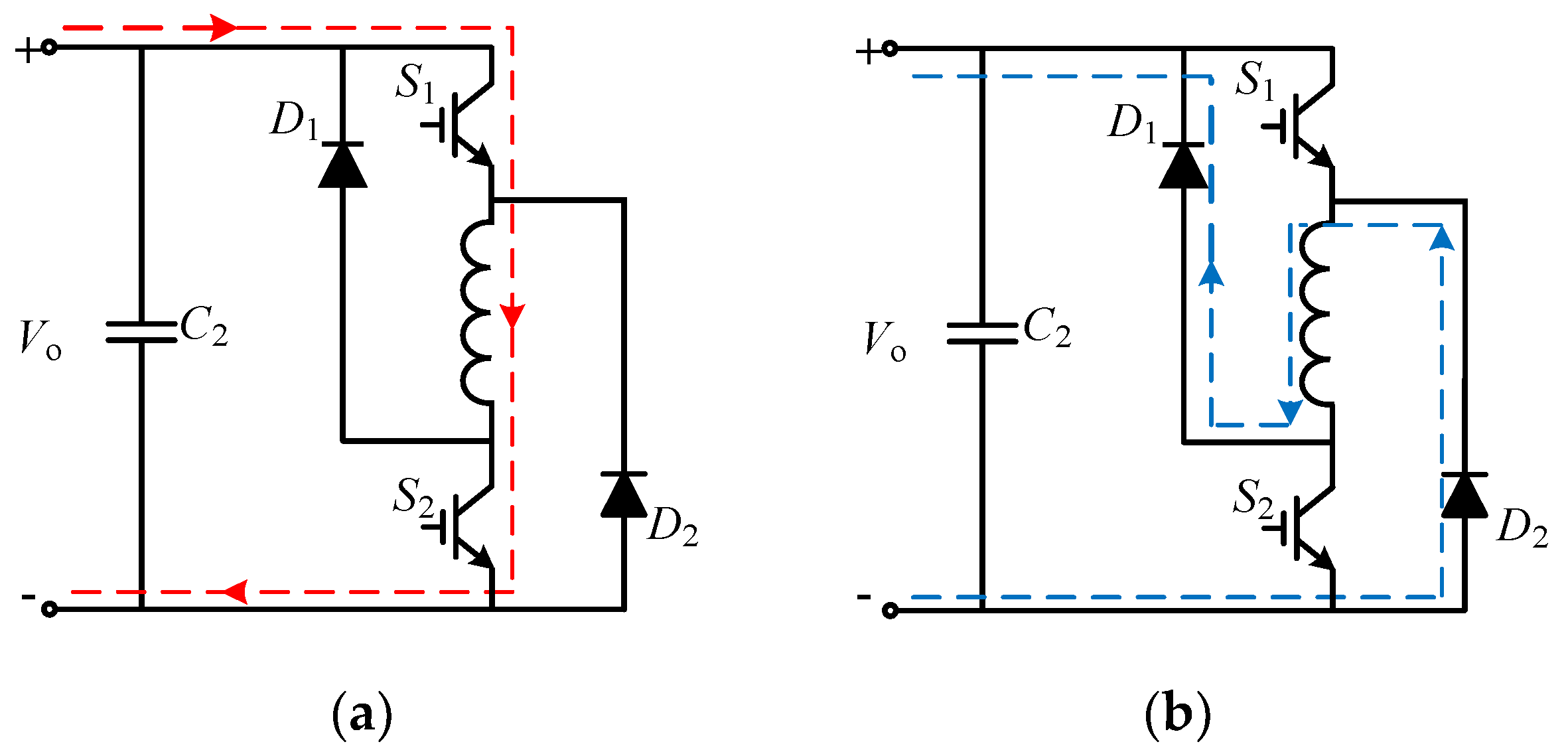
The operation of SRD can be divided into two stages: excitation section and freewheeling section. Traditional control methods practically adjust the voltage on the windings during excitation. The freewheeling section is often ignored as it is uncontrollable. The freewheeling section refers to the interval between the off state to the next on state of the switching device. The magnetic energy on the winding during this section that has not been completely converted into mechanical energy is turned back to the power supply through the diode. The excitation freewheeling circuit of one-phase winding of power converter is shown in
Figure 5.
The excitation circuit in
Figure 5a is also called a positive voltage circuit, and the freewheeling circuit is called a negative voltage circuit. Moreover, a zero-voltage circuit also exists under certain switching conditions. The zero-voltage loop refers to a loop in which one device is turned on while the other device is turned off. The current does not have any interaction with the outside and only flows internally as shown in
Figure 6. Compared with the negative voltage circuit, the winding of the zero-voltage circuit has no path to return energy to the power supply, thus avoiding frequent exchange of reactive power between the motor and the power supply. This feature has advantages such as being able to increase torque, to improve the utilization of the power converter capacity, to reduce the number of chopping, to suppress power supply voltage fluctuations, and to reduce torque ripple.
The chopper method corresponding to the negative voltage circuit is called hard chopper, and the chopper method corresponding to the zero-voltage circuit is called soft chopper [
23]. Switching devices in excitation circuit is not allowed to be open normally, which will stop the winding from being excited. Similarly, the switching device is not allowed to be normally closed in the freewheeling circuit, which will block the path of the energy on the winding to the power supply. The control of the SRD is generally applied during the excitation circuit, while the switching device is completely turned off during the freewheeling circuit. If the signal modulation is introduced during the excitation circuit, the motor cannot be properly excited, which will weaken the performance of the motor. In order to secure the smooth operation of the motor, signal modulation can be performed in the freewheeling circuit. The present study, based on the above analysis, adopts a soft chopper to reduce switches and to suppress the power supply voltage fluctuation and torque ripple.
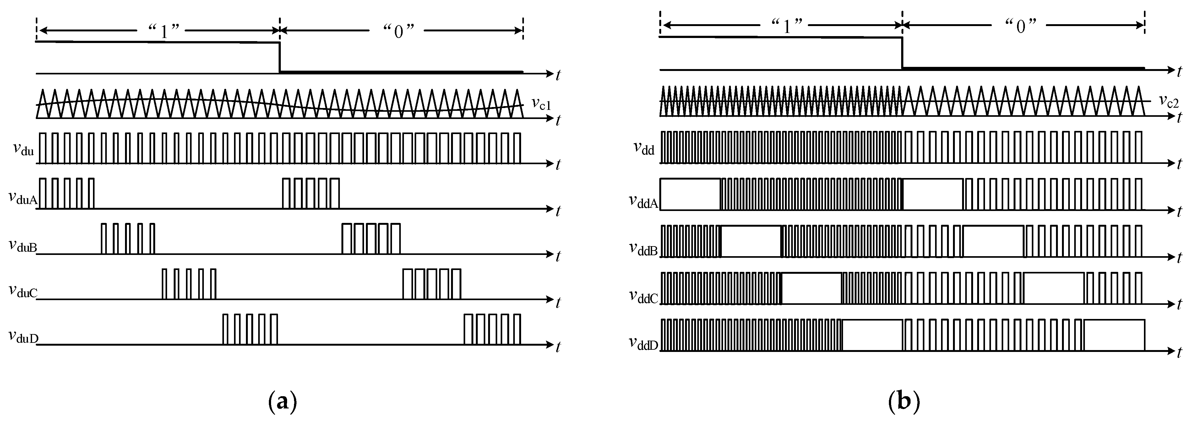
Figure 7 shows the driving signals of the switching devices for each phase.
It can be seen from the waveforms of the upper switching device driving signal in
Figure 7a that the frequency and amplitude of the carrier wave remain constant and do not change with the transmitted signal. The amplitude of the modulation wave
vc1 changes according to the difference between the actual speed and the reference speed. The driving signal waveforms of the 2 Frequency Shift Keying (2FSK) modulation of the lower switching devices are shown in
Figure 7b. When the regular triangle carrier wave transmits “1”, the frequency is
f1, and when it transmits “0”, the frequency is
f2. The amplitude and phase of the carrier remain unchanged. The PWM modulation wave
vc2 is a straight line, and its value is smaller than the maximum value of the carrier wave.
vc2 is taken as
where
VM is the maximum value of the carrier wave. Comparing the carrier wave with the PWM wave,
vc2 achieves the driving signal as a pulse, with a fixed duty cycle of 0.5. The lower switching devices of each phase remains normally closed during the excitation section, and the switching devices are controlled according to the driving signal
vdd in the freewheeling section, so that the bus voltage and current generate ripples with information. All signals such as the modulated 2FSK,
vc2, and the signals from
vddA to
vddD are all related to the transmitted signal. Meanwhile, the upper switching devices remain normally open in the freewheeling section. Soft chopping is therefore achieved.
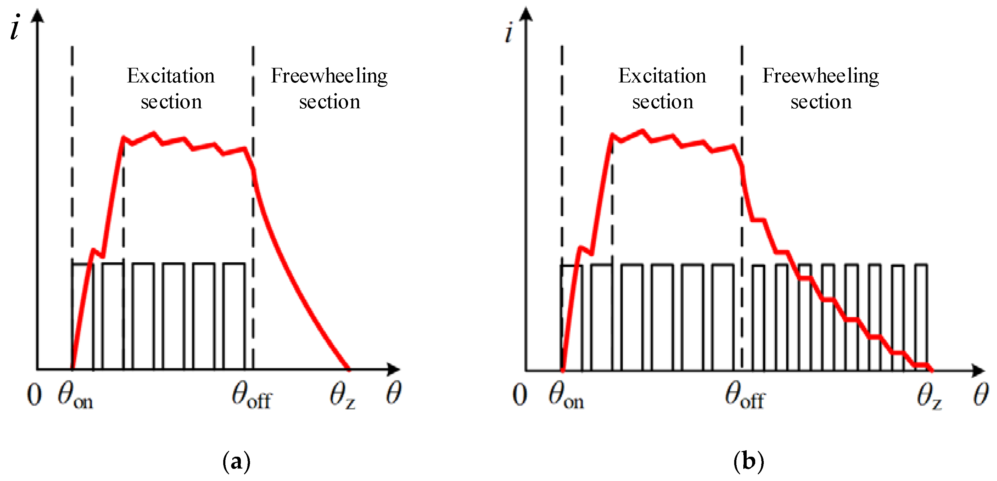
Due to the chopping in the freewheeling section, there will be changes in the phase current. The waveform of one phase current is shown in
Figure 8.
Assuming that the motor speed is the same in both cases, it can be seen from
Figure 8a,b that the current is the same in the excitation section but different in the freewheel section. The uncontrolled phase current in the freewheel section is quickly and smoothly reduced to zero in
Figure 8a, while the phase current with chopping in the freewheeling section gradually decreases in a step-like manner due to frequent switching between the negative-voltage loop and the zero-voltage loop. The time for the latter phase current to fall from the corresponding value at the turn-off angle to zero is about twice that for the former, and its current at each moment is also higher than that of the former. That means the phase current effective value of full chopper is larger, thus generating more electric torque.
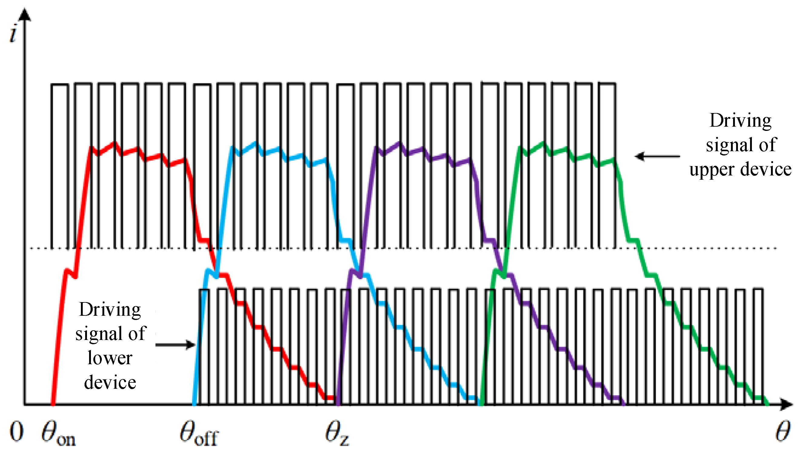
In every 15° interval, when one phase is in the excitation section, the other three phases are in the freewheeling section or the current has dropped to zero. As shown in
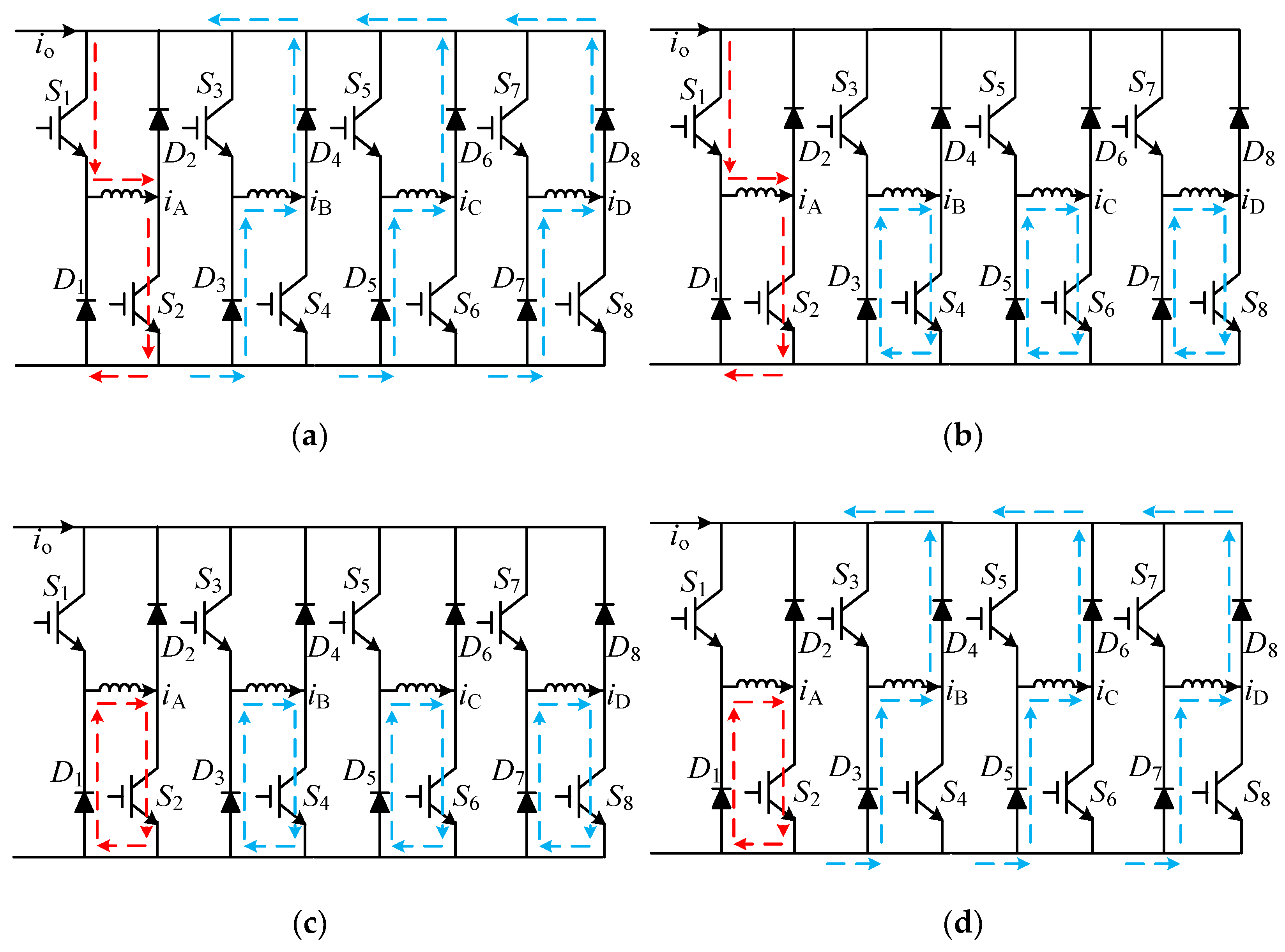
Figure 9, there will be a minimum of a two-phase current superimposed at each moment. Since the upper and lower switching devices have two states, on and off, there are four combined states in the entire period. As any one of the four phases is excited, the other three phases are in the freewheeling section. Taking phases A and B as an example, when phase B is excited, phase A is in freewheeling section. There are four states combined in total, as shown in
Figure 10, since carrier frequencies of the two phases, phase B with two states during excitation and phase A with two states during freewheeling, are different.
Take phase A in the excitation section as an example:
Case 1: Phase A is a positive voltage loop, and phases B, C, and D are all negative voltage loops. Therefore, the DC-bus current
io =
iA −
iB −
iC −
iD as shown in
Figure 10a.
Case 2: Phase A is a positive voltage loop, and phases B, C, and D are all zero-voltage loops. Therefore, the DC-bus current
io =
iA as shown in
Figure 10b.
Case 3: Phases A, B, C, and D are all zero-voltage loops. Therefore, the DC-bus current
io = 0 as shown in
Figure 10c.
Case 4: Phase A is a zero-voltage loop, and phases B, C, and D are all negative voltage loops. Therefore, the DC-bus current
io = −
iB −
iC −
iD as shown in
Figure 10d.
In the above four cases, the DC-bus current of case 2 and case 4 are positive and negative, respectively. The DC-bus current of case 3 gradually increases from a negative value, for which the final value is related to the conduction angle of SRD and DC voltage. Assume that the carrier frequencies of the upper and lower devices are
fu and
fd, respectively. At the same time, the duty cycle of the lower devices is constant at 0.5, while the duty cycle of the upper devices changes with the actual rotation speed. Referring to the above analysis of the bus current, in the case of
fu ≠
fd, the bus current will include the four combinations above. When
fu = 2
fd, it can be seen from
Figure 11 that the current waveform is not a smooth curve but jumps at the rising and falling edges of higher frequency (
fu). In a half cycle of the lower frequency (
fd), the DC-bus current switches between the two cases, while in the other half cycle, it switches between the other two cases. If SRD is not controlled with a closed loop, the driving signals of the upper device are single pulse, meaning that the devices remain normally closed. Meanwhile, the lower device turns on and off depending on
vdd and cooperates with the upper device to change between cases 1 and 2. Thus, the DC-bus current is relatively flat compared to that in
Figure 11, but there are also some jumps.
In the case of speed open-loop control, the carrier frequency of upper devices fu is zero. In order to reduce disturbance and to avoid introducing other frequency components, the carrier frequency fd of the lower devices should be chosen to meet the integer multiple of the commutation frequency. However, in the case of speed closed-loop control, fu is not equal to zero. Therefore, disturbance will occur in the frequency spectrum if fu is similar to fd, thus interfering with the demodulation of the signal. Therefore, fu should be appropriately larger or smaller than fd to ensure the detection of frequency fd.
4. Analysis of the DC-Bus Ripple
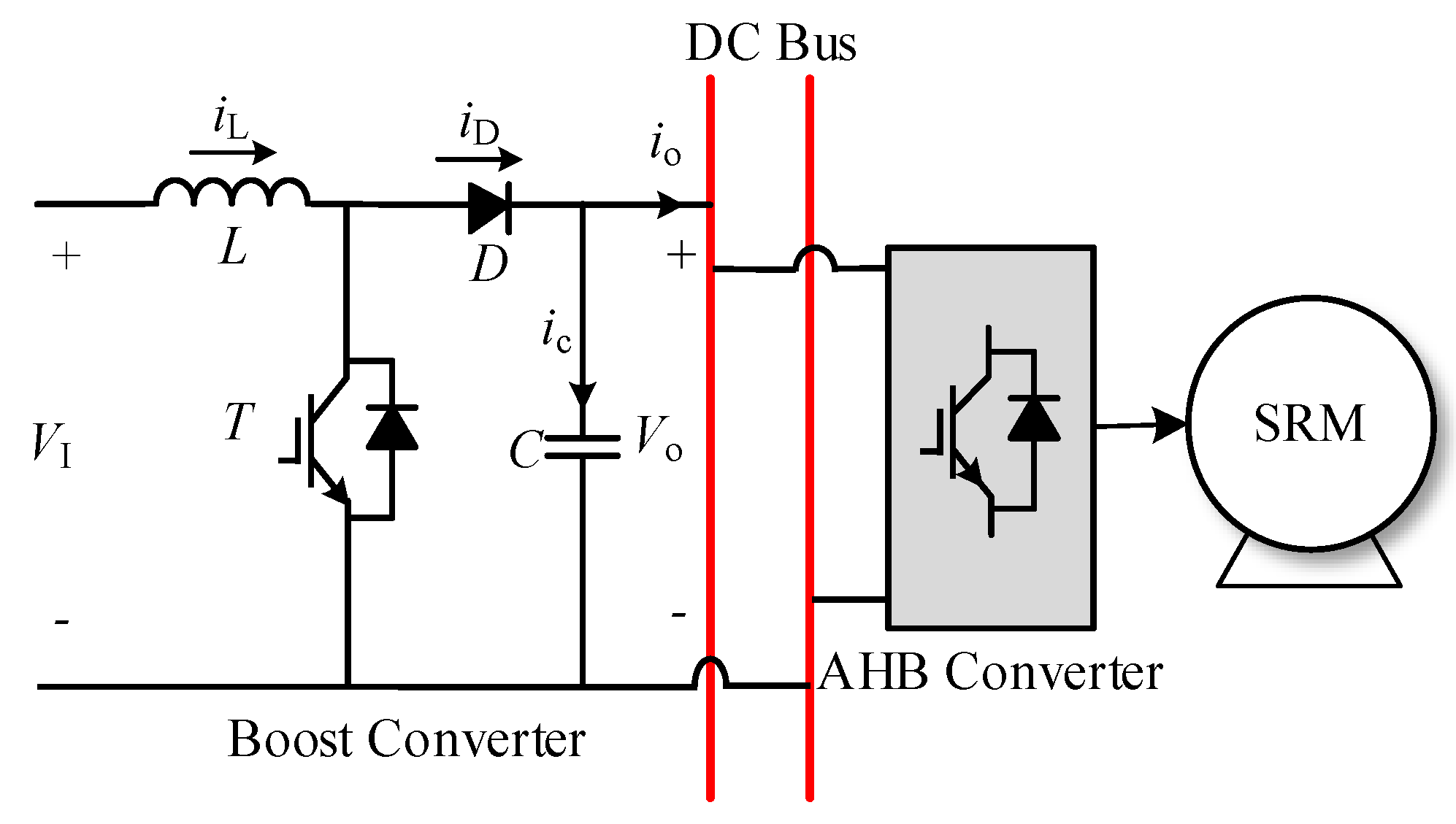
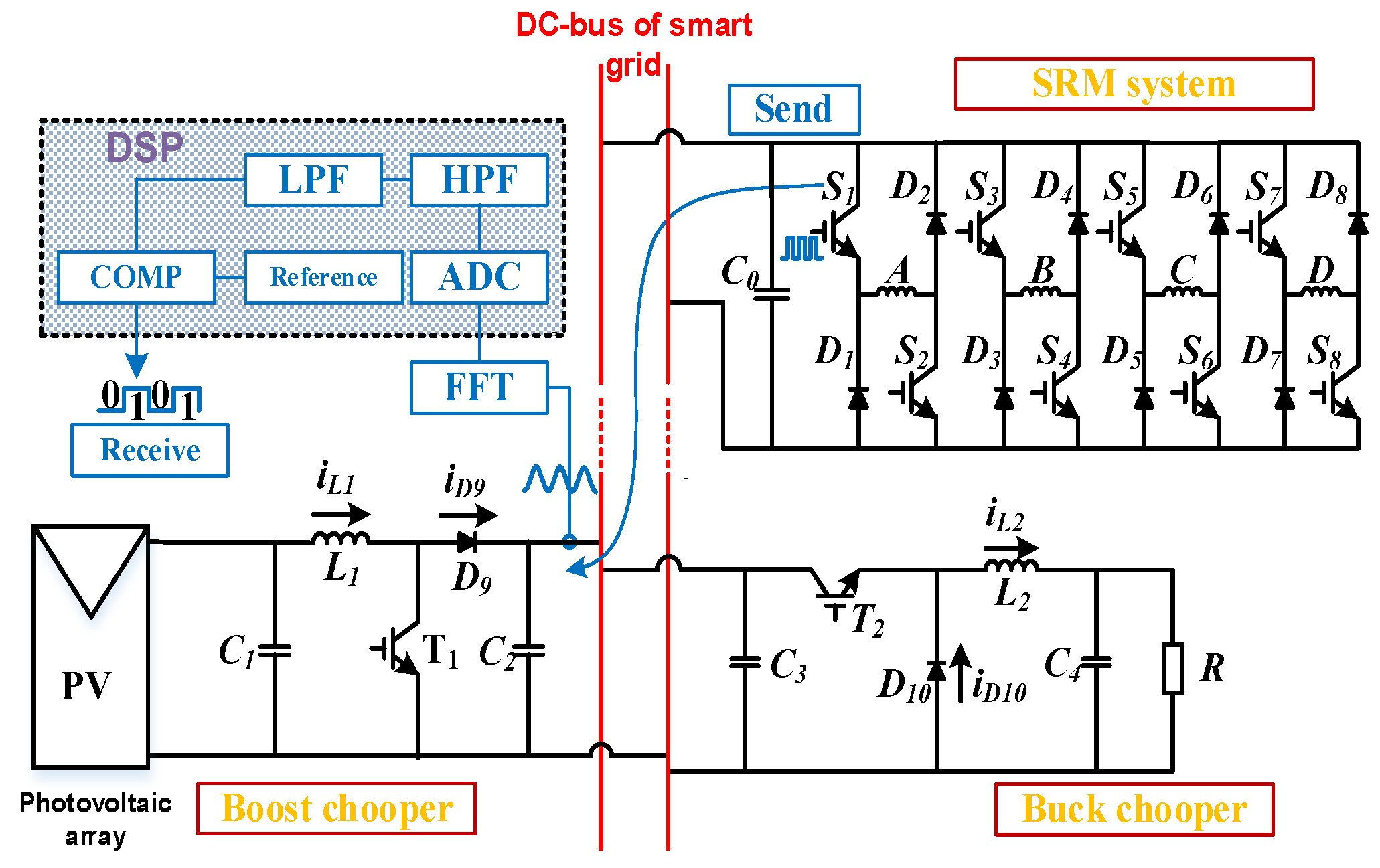
The synchronous transmission of energy and signal proposed in this paper is realized by using the ripple generated on the DC-bus from the switching of the motor power converter. The signal demodulation only calls for the switching ripple of SRD, but the system includes the commutation ripple and the switching ripple of the former boost circuit. The setup of the experimental system is shown in
Figure 12.
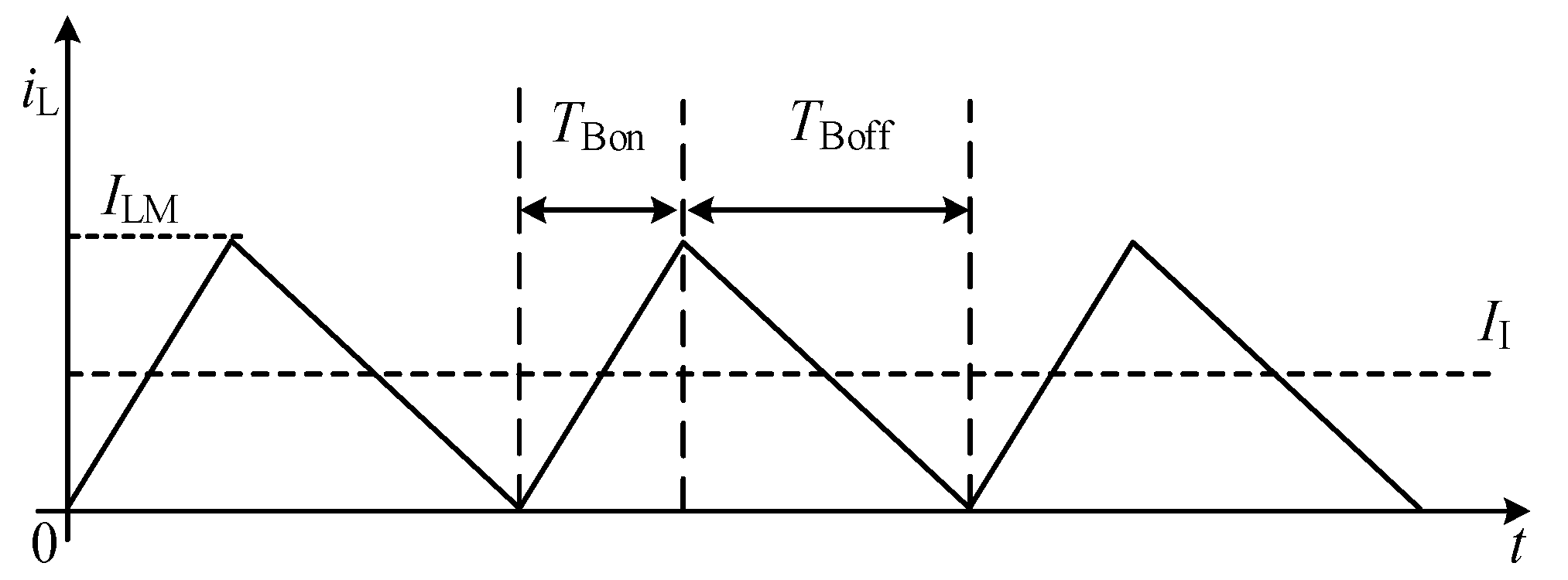
In the boost converter, the inductor current will pass through a critical point. Such charging and discharging processes add up to a complete cycle. The waveforms of current are shown in
Figure 13, where
ILM and
II are the maximum value and average value of the inductor current, respectively.
II is half of the maximum inductor current
ILM.
TBon and
TBoff are the turn-on and turn-off times of the boost circuit, respectively.
According to the law of conservation of energy,
Therefore, the critical inductance
LC is
where
TBoost is the switching period of the boost circuit,
d is the corresponding duty cycle, and
Io is the average value of the output current
io.
When the inductance is greater than
LC, the boost circuit is in continuous conduction mode (CCM). According to [
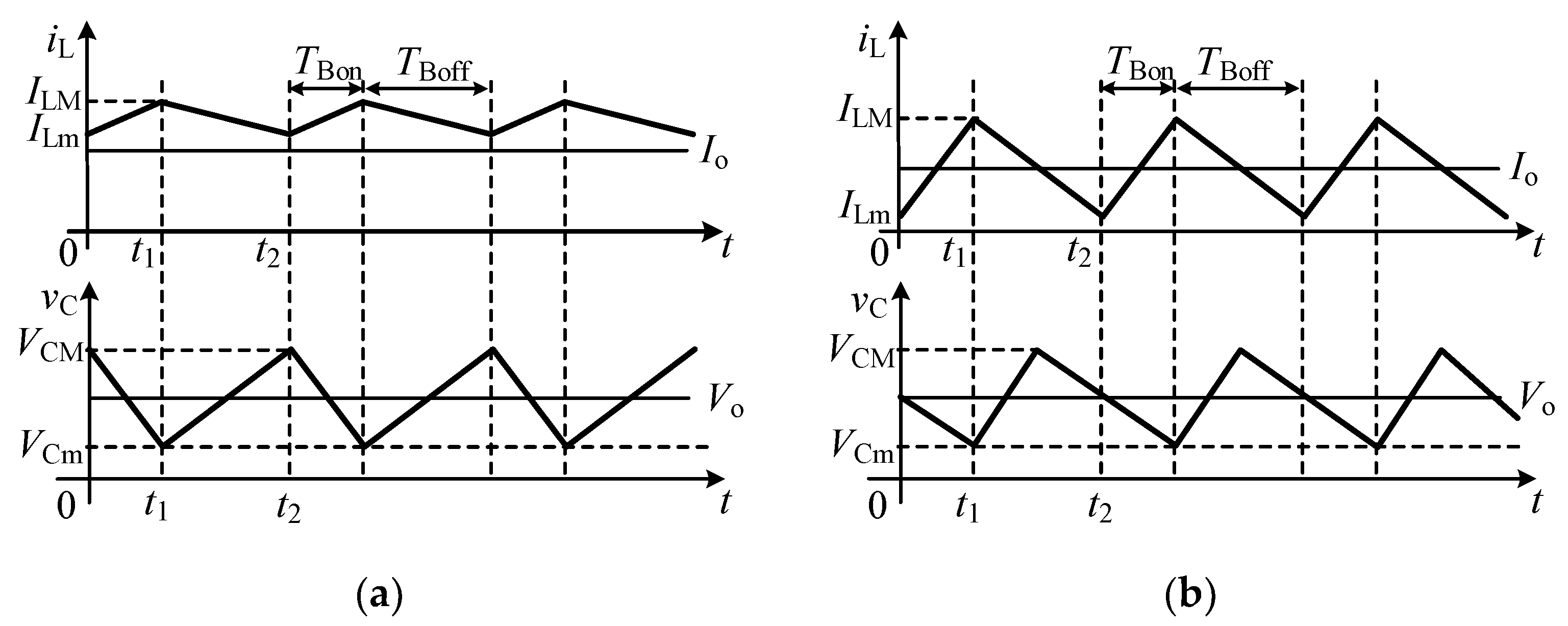
22], the boost circuit can be classified into complete inductor power supply mode (CISM) (
ILm >
Io) and incomplete inductor power supply mode (IISM) (
ILm <
Io). The waveforms of inductor current and capacitor voltage are shown in
Figure 14 below.
It can be seen from
Figure 12 that
io is the output current of the boost converter, which is equal to the sum of four phase currents of SRG. The one-phase current of SRD under linear model is
where
Lmin and
Lmax are the minimum and maximum inductance where the stator tooth pole coincides with the rotor slot axis, respectively.
For four phase 8/6 SRG, the conduction angle is 15°, assuming there is no overlap angle for any two phases. During operation, the angle
θz alters inside (
θ3, θ5) when the current drops to zero. The input current of the SRD
io can be expressed as
when
θz –
θoff ≤
θ2 –
θon,
When
θz −
θoff >
θ2 −
θon, we have
Since a step angle of an 8/6 SRD is 15°,
io is a periodic variable. Assuming that the motor speed is
r, the period is 1/(0.4
r). Thus, the average current in the above two cases are as follows:
By substituting
IO into Equation (11), the critical inductance can be obtained. The corresponding voltage ripples in CISM and IISM modes are as follows:
where
fBoost = 1/
TBoost. According to
Figure 12, the capacitor current and voltage should meet
Since the commutation frequency is much lower than the switching frequency of the boost circuit,
iD can be approximated as a stable continuous current
II. Let
t0 be the time corresponding to the minimum of current
io in the first cycle. When
io =
II, the corresponding time is labeled as
tI. Thus, the commutation voltage ripples of the motor can be expressed as
Normally,
io reaches the peak at
θ2, and
tI meets the following condition
Hence, in Equations (16) and (17), when
θI <
θz −
θoff, we have
In Equation (16), when
θI ≥
θz −
θoff
where
θ0 and
θI are the angles corresponding to
t0 and
tI, respectively. It can be seen from the above equations that the amplitude of the commutation ripple is proportional to the excitation voltage and turn-off angle of SRD and is inversely proportional to the rotational angular speed of the motor.
For the ripples caused by the driving signal of the SRD, there will be multiple driving signal cycles during one oscillation period of
ic, since the frequency of the driving signal is greater than the commutation frequency. Once the cycle width of the driving signal is determined, the length of the integration interval is also determined. However,
ic in the corresponding interval is different, so the maximum value of the ripple amplitude should be taken as
where
tk and
tIk are the moments corresponding to the rising and falling edges of the drive signal, respectively. The amplitude of the ripple is inversely proportional to the frequency of the drive signal and DC-bus capacitance.
5. Modulation and Demodulation Methods
Usually many converters and loads are connected to the DC-bus. Switching noise disturbance exists among these devices, and the amplitude of the switching harmonics is large. Consequently, both the zero-crossing detection method and the envelope detection method will be interfered with and bit errors will occur. This paper adopts the Fourier transform method to analyze the frequency component corresponding to “1” or “0” to realize data demodulation.
The signals on the DC-bus modulated by the modulation circuit can be expressed as
where c(t) should satisfy
f1 and
f2 are the carrier frequencies corresponding to the signals “1” and “0”, respectively. When calculating the amplitude of signal
f1, A
2 is regarded as the amplitude of noise. According to Euler’s identity, the exponential form of Equation (28) is expressed as
where
n is an integer.
f1 and Fourier calculation period
Ts should satisfy
In Equation (32), m1 is an integer and fs is the fundamental frequency. It is apparent that the signal with frequency f1 is the m1th-order harmonic component of s(t). Therefore, the amplitude of m1th-order harmonic component can be determined by Fn.
In order to eliminate the influence of frequency
f2 on
f1,
The above Equation shows that f2 is also an integer multiple of fs, so it satisfies the orthogonal relationship with f1 in the Fourier calculation period.
2FSK digital demodulation algorithm is to calculate the amplitude of the corresponding carrier through Fourier transform. According to Nyquist theorem, the sampling frequency
fsmp should satisfy
Assuming that
N points are sampled at each cycle
Ts with a frequency
fsmp, then
The sampling sequence is {
s(
n),
n = 0, 1, 2…,
N−1}, then the discrete Fourier transform (DFT) of
s(
n) is
According to Equation (32),
f1 is an integer multiple of the fundamental frequency
fs, and then, the frequency component of
f1 is the
m1th-order harmonic of the DFT transform in Equation (36). Thus, its amplitude is
Because the sending and the receiving terminal of the system cannot achieve synchronization, in order to reduce the delay caused by performing a DFT transformation every cycle, a DFT transformation is performed when a value is sampled. Since this will increase the calculation of the algorithm, the iterative algorithm of DFT can be used.
Supposing that the current sequence is {
s(0),
s(1),…,
s(
N−1)} and that the next sequence is {
s(1),
s(2),…,
s(
N)}, the amplitude of the
m1th-order harmonic calculated in this sequence is
because
Equation (38) can be written as
Compared to the original discrete Fourier calculation, it can be seen from the above iteration formula that each operation only needs to execute two addition and subtraction instructions and one multiplication instruction, which greatly reduces the amount of calculation. Because the
N sampling points are taken at each cycle
Ts with the frequency
fsmp, when the sampling is refreshed, it can be considered that the window of length
Ts moves by one sampling interval, and an amplitude value of frequency
f1 is obtained. The demodulation process is shown in
Figure 15 below.
Strictly speaking, the addition of signal modulation strategy will certainly impact the operation performance of SRD system since extra voltage ripples are injected onto the power bus. For Amplitude Shift Keying (ASK), the voltage ripple amplitude must be maintained at a relatively high level in order to guarantee the demodulation accuracy. With regards to FSK, the data is carried by high frequency voltage ripples and demodulated by the Fast Fourier Transform (FFT) method. Hence, the voltage ripple for carrying data can be configured with a smaller amplitude since ripple frequency is used for demodulation. In addition, 2FSK is adopted for power and signal synchronous transmission but only in the freewheeling operation stage. Note that conventional control strategies for SRD, such as Angular Position Control (APC), Current Chopper Control (CCC), and Voltage Control (VC), are only activated in the excitation stage of SRD. Hence, the signal modulation applied only in the freewheeling stage will not degrade the control performance of SRD. It can be found that, under the proposed modulation strategy, the Root Mean Square (RMS) value of phase current is larger, which is beneficial for producing higher electromagnetic torque.
6. Simulation and Experiments
In order to verify the feasibility of the proposed method, MATLAB/Simulink was adopted to build the simulation system.
The transmitted signal is a square wave with a frequency of 50 Hz. The two carrier frequencies used by 2FSK are set to 10 kHz and 8 kHz, and the output voltage of the boost converter is 57V.
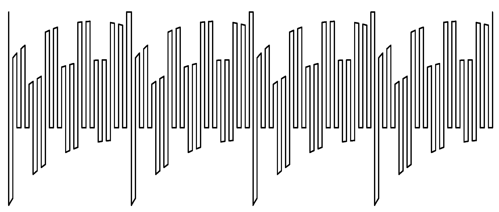
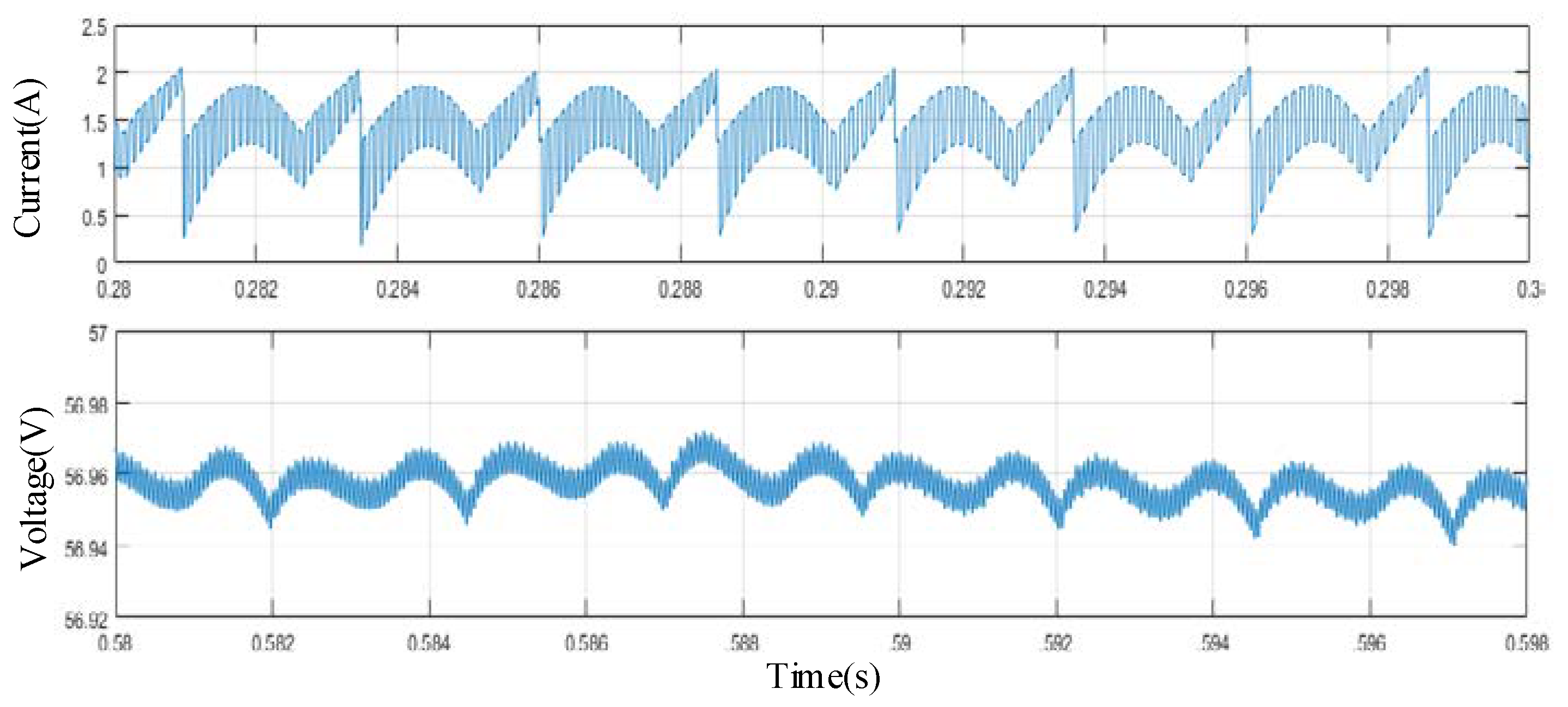
It can be seen from
Figure 16 that, when the rotation speed is 1000 r/min, the commutation frequency is 400 Hz. The current of DC-bus is not a smooth curve, and there is a jump periodically.
Signal modulation is performed on the upper and the lower devices. The waveform of a DC-bus current is shown in
Figure 17. The figure shows the current waveforms corresponding to the signal modulation of the upper and the lower devices at the same time. The two sets of simulated waveforms are almost identical, which is in accordance with the structural characteristics of the asymmetrical half-bridge power converter of the SRD.
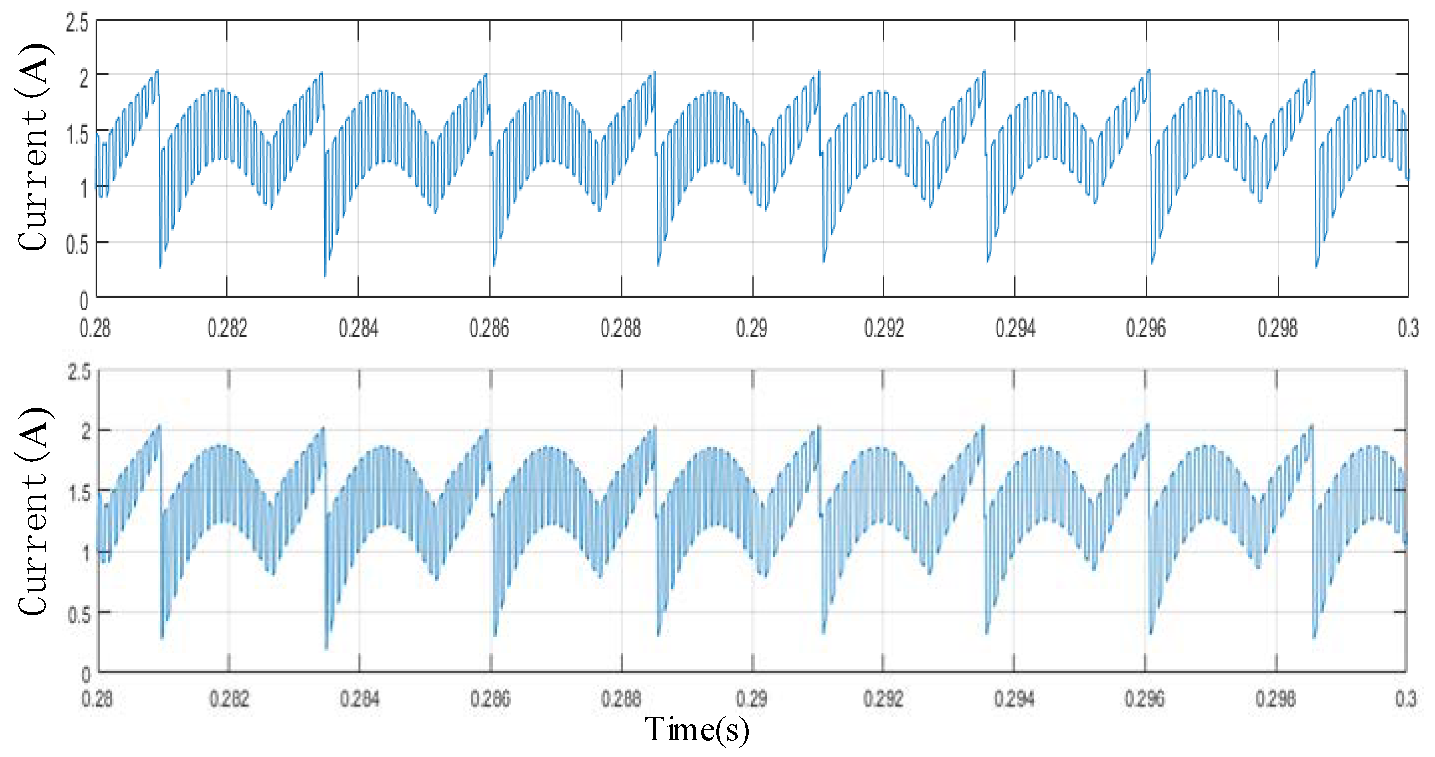
The current shown in
Figure 18 is the waveform when the conduction angle is 15°. Unlike the bus current with a conduction angle of 20° in
Figure 17, the current rises and falls only once per cycle and does not rise again after the fall. The reason for this difference is that, at 20° conduction angle, there is an overlap angle of 5° between the former and the latter phases of the motor. The direction of the current is consistent with the negative direction of the DC-bus current after the turn-off angle. The DC-bus current superimposes at this position to produce a sudden change.
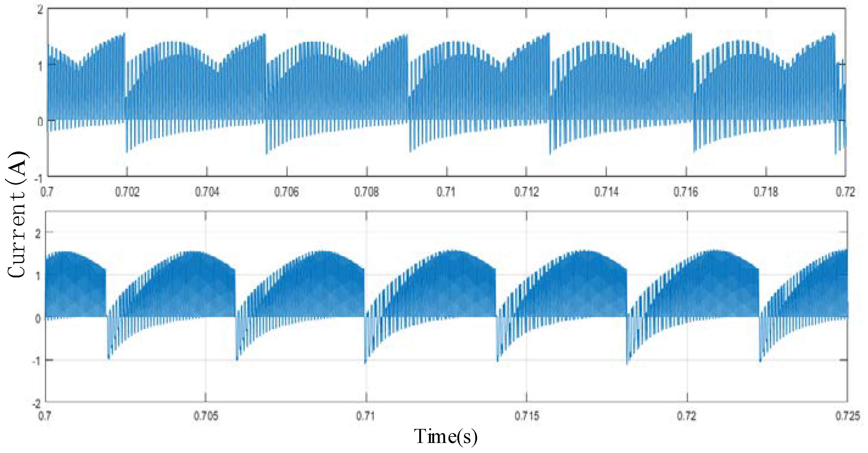
Figure 19 shows the DC-bus currents corresponding to the conduction angles of 15° and 20° under the speed closed-loop control. To verify the above analysis, the carrier frequency of upper devices is set to twice that of the lower devices. In this case, the DC-bus current switches in four cases and the minimum value is negative, which is consistent with the above analysis. The curve obtained after the analysis of frequency spectrum is shown in
Figure 20 below.
Figure 21 is a transmission signal waveform obtained after threshold value judgment.
It can be seen from
Figure 21 that transmitted signal can be successfully recovered at the receiving terminal after being modulated by the proposed method and that there is a certain delay compared with the original signal. Moreover, if the SRD adopts open-loop speed control, the carrier frequency of the upper devices is 0, which also meets a certain difference with that of the lower ones, and achieves demodulation of the signal.
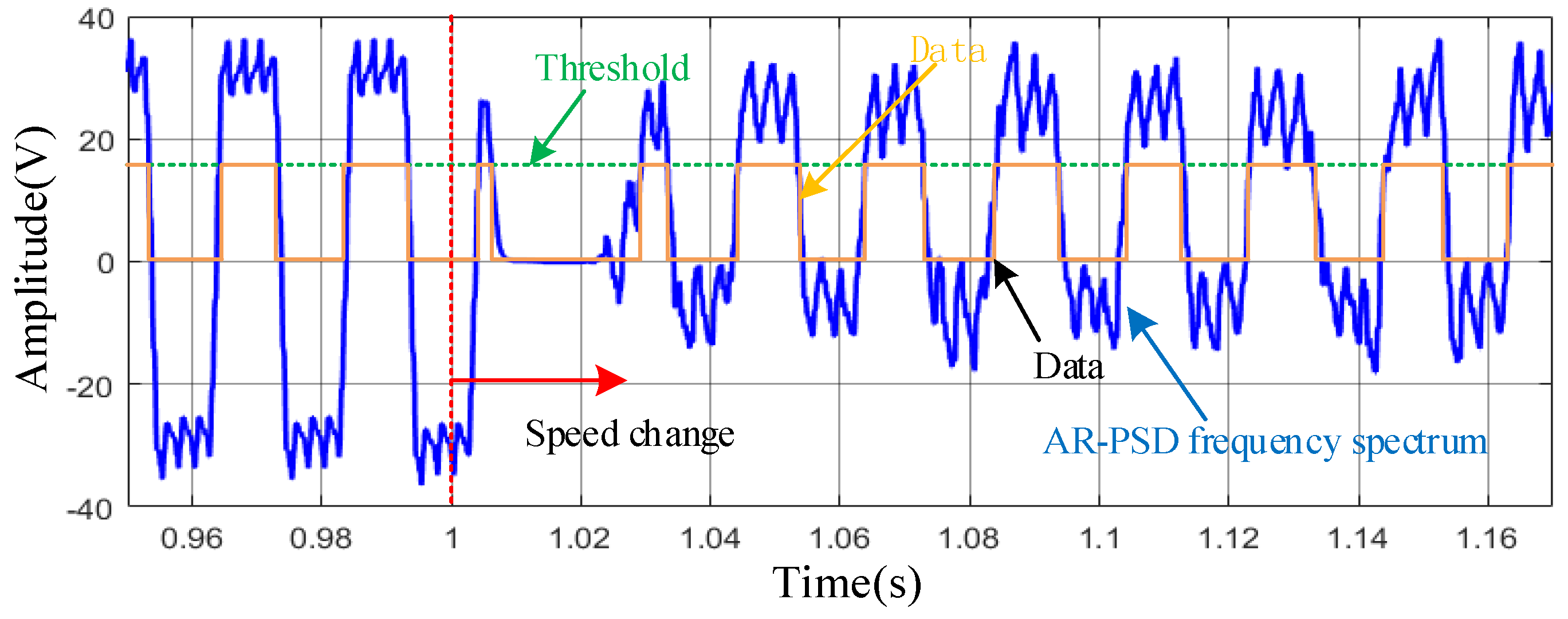
In order to reveal the goodness of the proposed power and signal composite modulation strategy, the data is transmitted under three operation cases: (1) the speed is changed from 1000 r/min to 800 r/min; (2) the load is reduced from 20 Nm to15 Nm; and (3) the transmission line is lengthened to 500 m with 4 Ohm resistance. The received signal is demodulated, and the frequency spectrum as well as the data is presented in
Figure 22,
Figure 23 and
Figure 24, respectively, as shown below.
It can be seen that the demodulated data can be greatly influenced by the speed change. During the speed change transient, the width of each demodulated data is narrowed, which might degrade the data transmission performance. However, the data can be accurately demodulated as the speed is stabilized to the targeted reference, as shown in
Figure 22. As the load is reduced from 20 Nm to 15 Nm, the data can be demodulated without deterioration, as shown in
Figure 23. The transmission line is lengthened to 350 m with 4 Ohm resistance, and the frequency spectrum and demodulated data of the received signal are presented in
Figure 24. This result show that the frequency spectrum can still maintain high amplitude for data demodulation, which is good for anti-interference. These above results interpret the good performance of the proposed strategy.
If the carrier frequencies of the upper and lower devices are both set as 10 kHz, the result of the DC-bus current after spectrum analysis is shown in
Figure 25. It can be seen from the analysis that the spectrum is much worse than that in
Figure 20. Therefore, such a setting will cause bit errors in demodulation. In order to reduce the bit error rate, the carrier frequency of the upper devices needs to avoid being close to the lower ones.
Experimental platform is built according to the simulation model, as shown in
Figure 26.
The schematic of the experimental system is shown in
Figure 27. When the signal is not transmitted or signal “0” is transmitted, the upper and the lower devices of the excitation section maintain normal operation. When signal “1” is transmitted, the upper and lower devices are simultaneously applied by a signal of frequency
f1 = 1.6 kHz. The sampling frequency is 16 kHz, and the calculation period
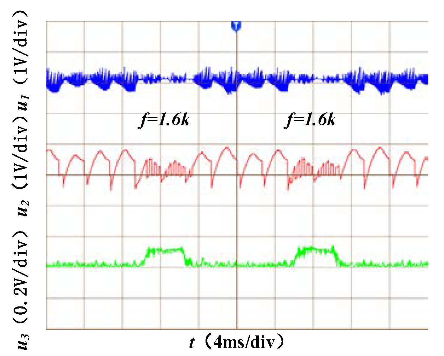
Ts of Discrete Fourier Transform (DFT) algorithm are set to 3.125 ms. The experimental waveform is shown in
Figure 28, where
u1 is the DC-bus voltage ripple signal, including the commutation ripples superimposed with the switching harmonic;
u2 is the DC-bus current signal; and
u3 is the waveform of harmonic amplitude.
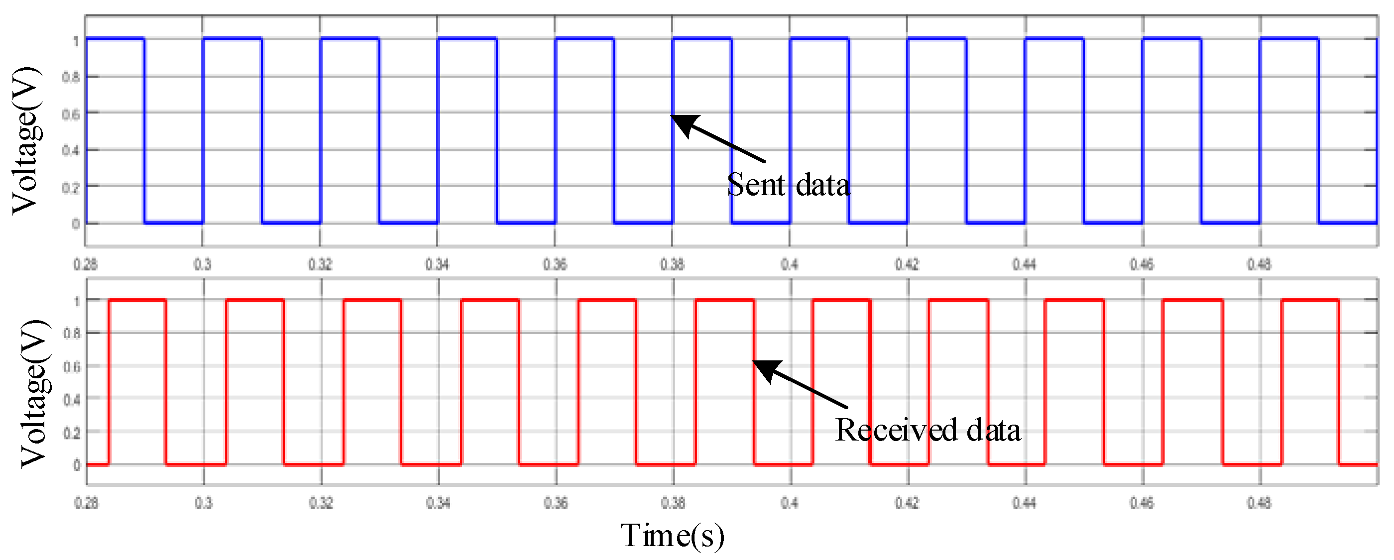
The signals at the transmitter and receiver are shown in
Figure 29, where
u1 and
u2 are the transmitted and received signals, respectively. It can be seen that each signal error between
u1 and
u2 does not exceed one DFT cycle.


