Article

A Novel Three-Phase Current Source Rectifier Based on an Asymmetrical Structure to Reduce Stress on Semiconductor Devices

1
School of Electric Power Engineering, South China University of Technology, Guangzhou 510641, China
2
School of Electronic Engineering, Dongguan University of Technology, Dongguan 523808, China
*
Author to whom correspondence should be addressed.
Energies 2020, 13(13), 3331; https://doi.org/10.3390/en13133331
Submission received: 14 May 2020 / Revised: 17 June 2020 / Accepted: 23 June 2020 / Published: 30 June 2020

Abstract

:
This paper presents a novel three-phase current source rectifier (CSR) for AC/DC step-down voltage conversion to reduce voltage and current stress. The proposed converter features an asymmetrical connection between upper and lower arms compared with conventional CSRs, but has the same number of devices. With the proposed asymmetrical structure and modified space vector pulse width modulation (SVPWM) scheme, half of transistors only need to withstand half of the line-to-line voltage rather than the full line-to-line voltage, and its DC link current can be shared by multiple switches in freewheeling periods. Therefore, it is able to bring about a significant reduction in voltage and current stress, allowing for an improvement in the converter without additional cost. The topological structure, operation principles, and comparative analysis are specifically presented. Finally, an experimental prototype is built up to verify the performance of the proposed converter.

Graphical Abstract

1. Introduction

The three-phase CSR, also known as the buck-type rectifier, is widely used in AC/DC conversion systems, such as fast electric vehicle chargers, energy storage devices, communication power supplies, adjustable speed drives, wind power generation systems, high power applications, etc. [1,2,3,4,5,6,7,8]. Compared with the conventional boost-type converter [9,10,11], the aforementioned buck-type CSR systems provide a smaller AC input filter, inrush current limiting capability, and controllable step-down voltage conversion with a power factor correction (PFC) function for the abovementioned industrial applications [12,13]. Hence, the three-phase CSR has been a popular research area and has attracted a lot of attention over the past few years.
There are several three-phase CSRs introduced in most of the literature, including the six-switch CSR [14], three-phase four-wire CSR [15], current doubler CSR [16], matrix-type CSR [17], three-switch CSR [18], swiss-type CSR [19], delta-type CSR [20], split freewheeling diode CSR [21], etc. Another kind of isolated CSR is achieved with a high-frequency transformer [22,23,24,25,26,27]. It could provide electrical isolation between the input and output to ensure safe operation, but it has a higher cost and the power density could be decreased. Meanwhile, the design of high-frequency transformers and modulation schemes is more difficult for researchers. Therefore, the isolated CSR is not suitable for most of industrial applications. Moreover, both CSRs could obtain a sinusoidal input current and constant DC output voltage, as well as high stress on semiconductor devices, which is not expected in practice.
Generally, CSRs usually use the transistor (IGBT or MOSFET) in series with a diode to form switches, so the switches would have a reverse blocking capability and can block the AC current. Inevitably, there would be a reversed body diode in the transistors due to the production process [28,29]. Although a reverse blocking IGBT (RB-IGBT) has been developed in recent years [30,31,32], it has a higher switching loss. Unlike the boost-type voltage source rectifier (VSR), the body diodes of the transistors are ignored and are not utilized in most applications of the conventional CSRs. If we also consider the body diode as a current flowing device in the CSR circuit, the circuit will exhibit other superior characteristics that are distinct from the conventional topological structures. Therefore, a new current path with the body diode is obtained by changing the inflow terminal or outflow terminal to restructure the CSR topology in this paper. The proposed CSR features an asymmetrical topological structure and would have reduced stress on semiconductor devices. It means that half of transistors on low voltage stress can be achieved in PFC operation, and the proposed converter could have a higher efficiency at a low modulation index due to the multiple freewheeling paths. Compared with the conventional CSR, the detailed advantages of the proposed CSR are summarized as follows:
(1) Low cost without additional hardware;
(2) Half of transistors on lower voltage stress 1/2 VL_im;
(3) Low current stress 1/3 io in freewheeling period;
(4) High efficiency at low modulation index;
(5) Smaller output filter for CSR system.
According to the above analysis, the rest of the paper is organized into five sections. In Section 2, the proposed CSR structure is introduced and compared to the conventional CSR. Then the basic operation principle and stress characteristics are analyzed in Section 3. Detailed discussions are carried out in Section 4. As a proof of concept, the proposed CSR is performed on a prototype in Section 5 and the conclusion is drawn in Section 6. All theoretical analysis and experimental results show that the proposed CSR is a suitable topology for step-down voltage applications.

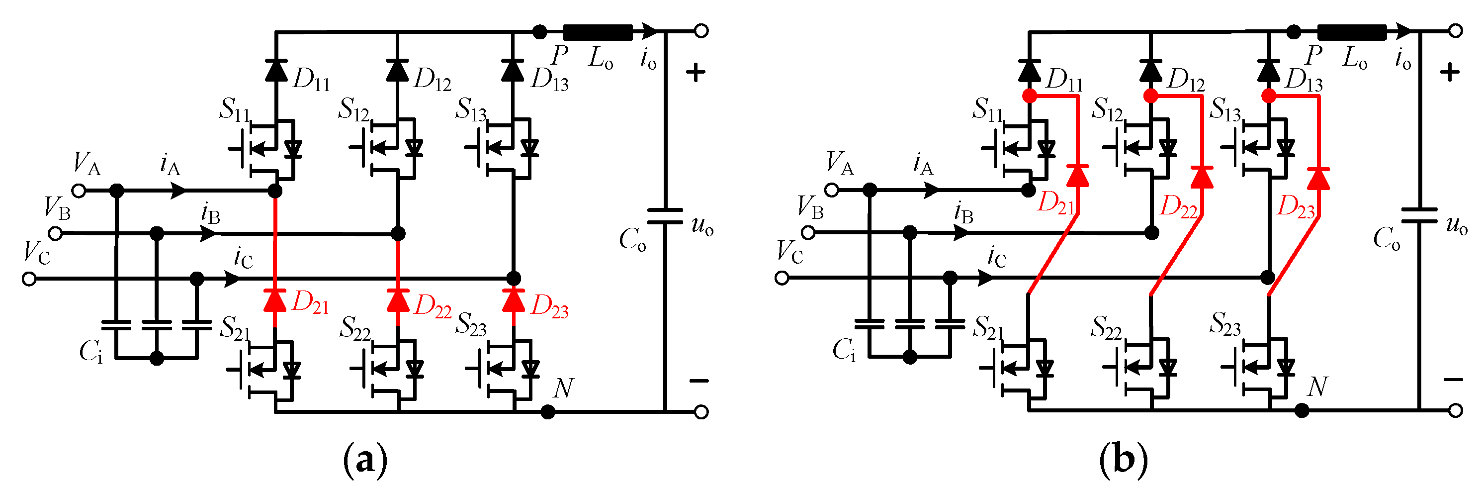
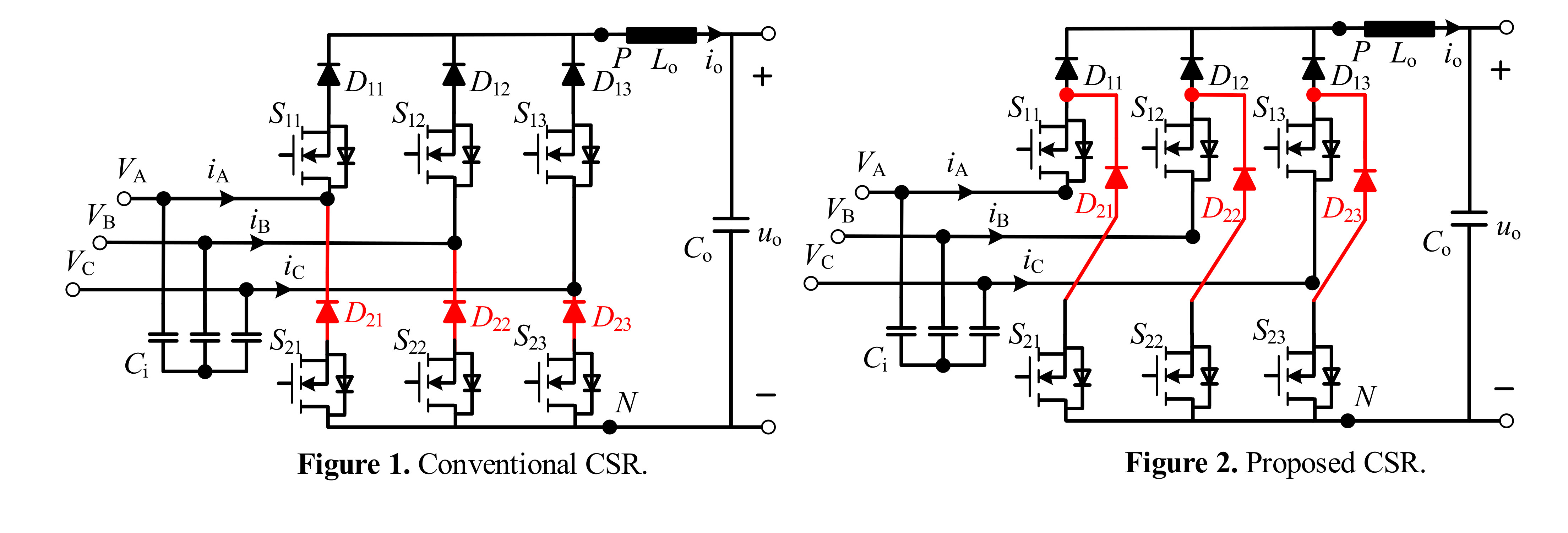
2. Topological Structure

Figure 1a shows the conventional standard six-switch CSR topological structure, there are three bridge arms and each arm can be divided into symmetrical upper and lower switch parts. Taking the arm of A phase as an example, the outflow terminal of the A phase current is the same with the inflow terminal and they are both at the symmetrical point.
Different from the conventional CSR structure, the outflow terminal of the proposed CSR in Figure 1b is not the same with the inflow terminal but is connected between the diode and the transistor on the upper arms. This is an asymmetric CSR, while the two topological structures have the same number of devices. As can be seen, compared with the conventional CSR in Figure 1a, the body diodes on the upper arms are added to the current path of the proposed CSR. With the modified structure, the current path in the proposed CSR has a minor change.
It should be noted that another topological structure can be constructed by changing the inflow terminal rather than the outflow terminal and the structure would have similar characteristics, but this is omitted for the sake of brevity.

3. Basic Operation Principle and Stress Characteristics of the Proposed CSR

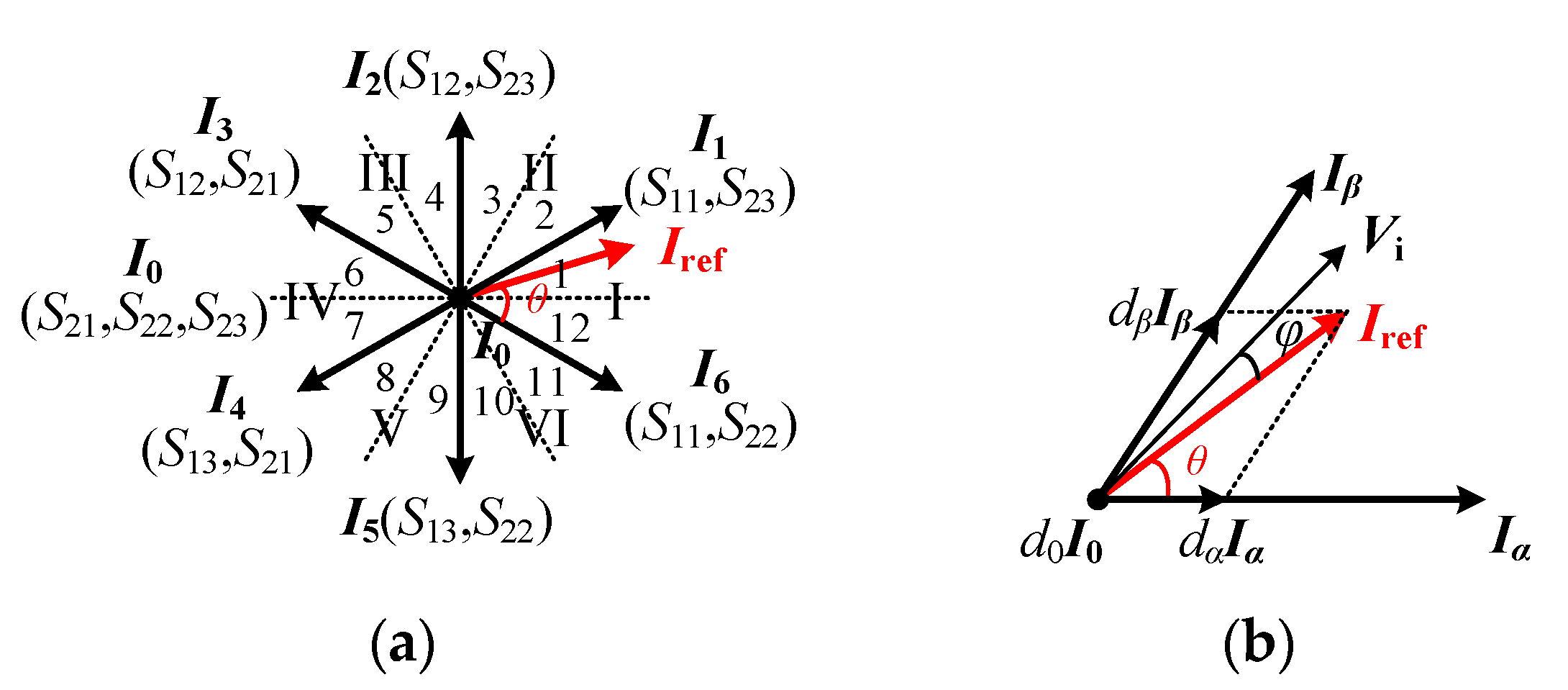
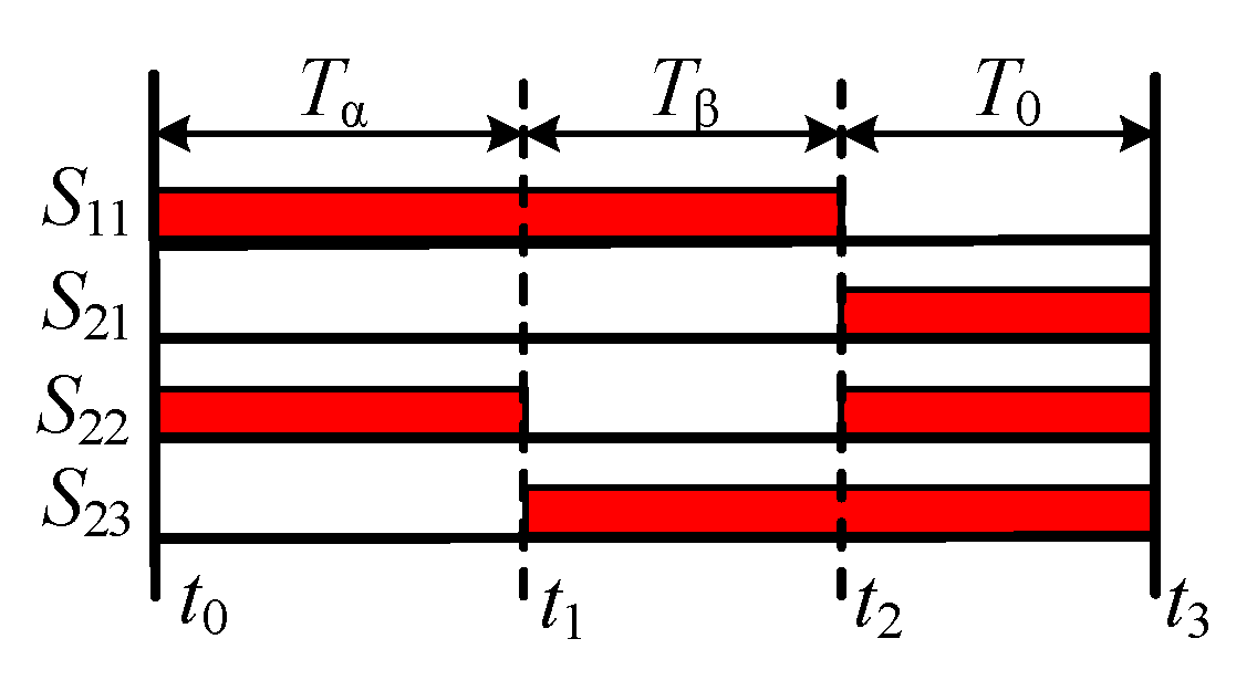
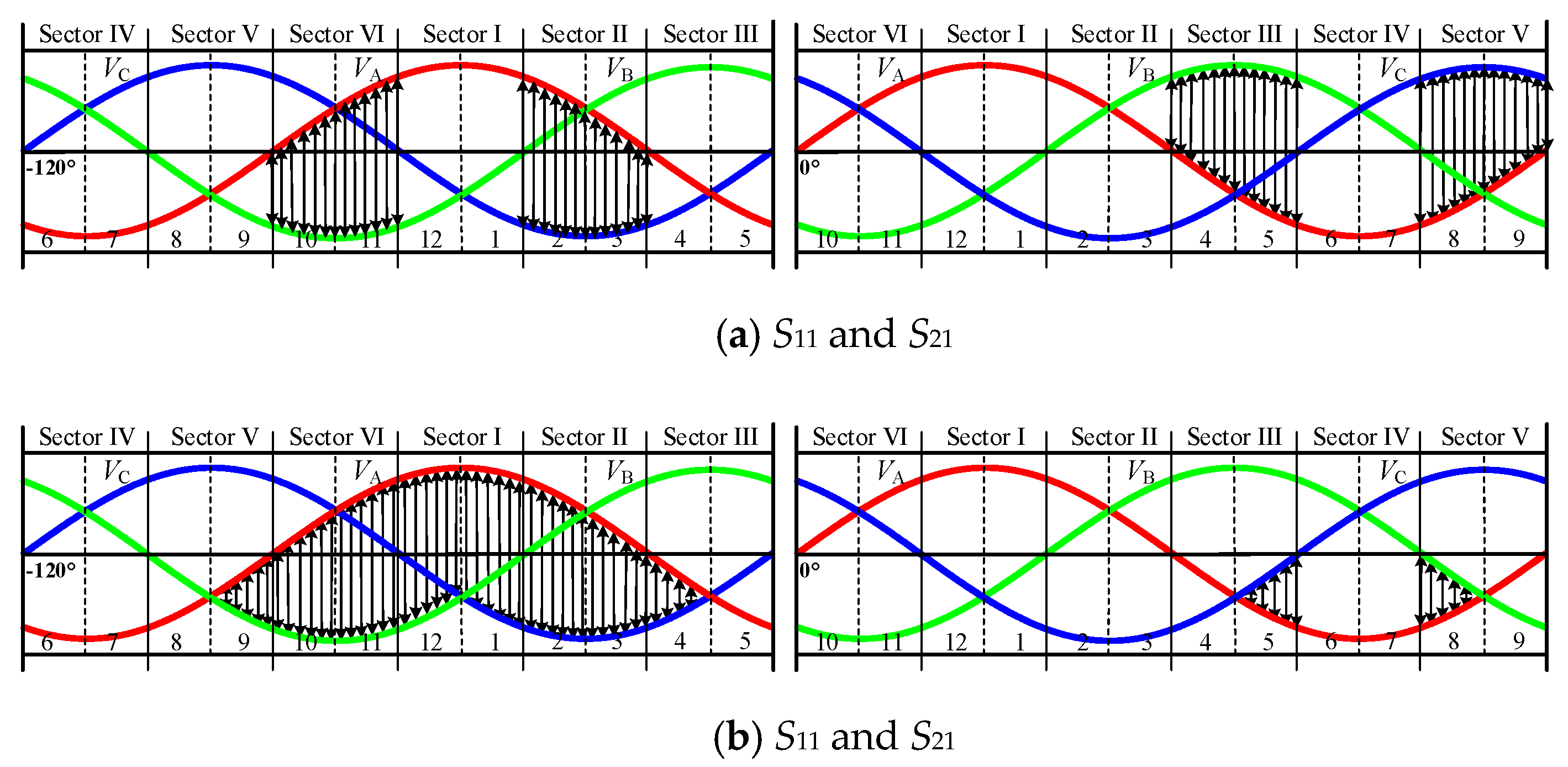
3.1. Modulation Scheme

SVPWM is one of the most popular modulation schemes for CSRs. Similar to three-phase VSRs, the core idea of the SVPWM for three-phase CSRs is the input reference current space vector Iref synthesis. Firstly, in order to ensure that the output side is not opened and the input side is not shorted at any time for the proposed CSR, there exist seven switching states, as listed in Table 1. The existing switching states can be classified into six active vectors and one zero vector, where I1I6 are the active vectors, and I0 is the zero vector.
In order to obtain the given sine current waveforms, the input reference current space vector Iref must be constructed as a space rotating current vector with angular velocity w and modulus length Iim, and the running trajectory of the corresponding input reference current vector would be a circular trajectory. Therefore, for the sake of the above objectives, it is very important to select the appropriate current vector in Table 1 to synthesize the input reference current vector Iref during one switching period.
To analyze the principle of vector synthesis, an ideal three-phase voltage is assumed in Figure 2. In each input cycle exists six sectors and every sector is further divided into two regions. Figure 3 shows the SVPWM schematic diagram of the proposed CSR.
According to [13], the input reference current space vector Iref is synthesized by two active vectors and one zero vector. It can be calculated as:
I ref = d α I α + d β I β + d 0 I 0
where dα, dβ, and d0 are the duty cycles for different vectors, respectively. During one switching period Ts, the duration formulas of all the vectors are expressed as:
T α = d α T s = m T s sin ( π / 3 θ ) T β = d β T s = m T s sin θ T 0 = T s T α T β
where m is the modulation index and m [0, 1]; θ is the sector angle. Then the average DC output voltage in one switching period can be calculated as:
u o = 1.5 m V im cos ϕ
where Vim is the amplitude of the input phase voltage, φ is the input displacement angle. Therefore, when m = 1, the maximum DC output voltage 1.5 Vim can be achieved at unity power factor operation.

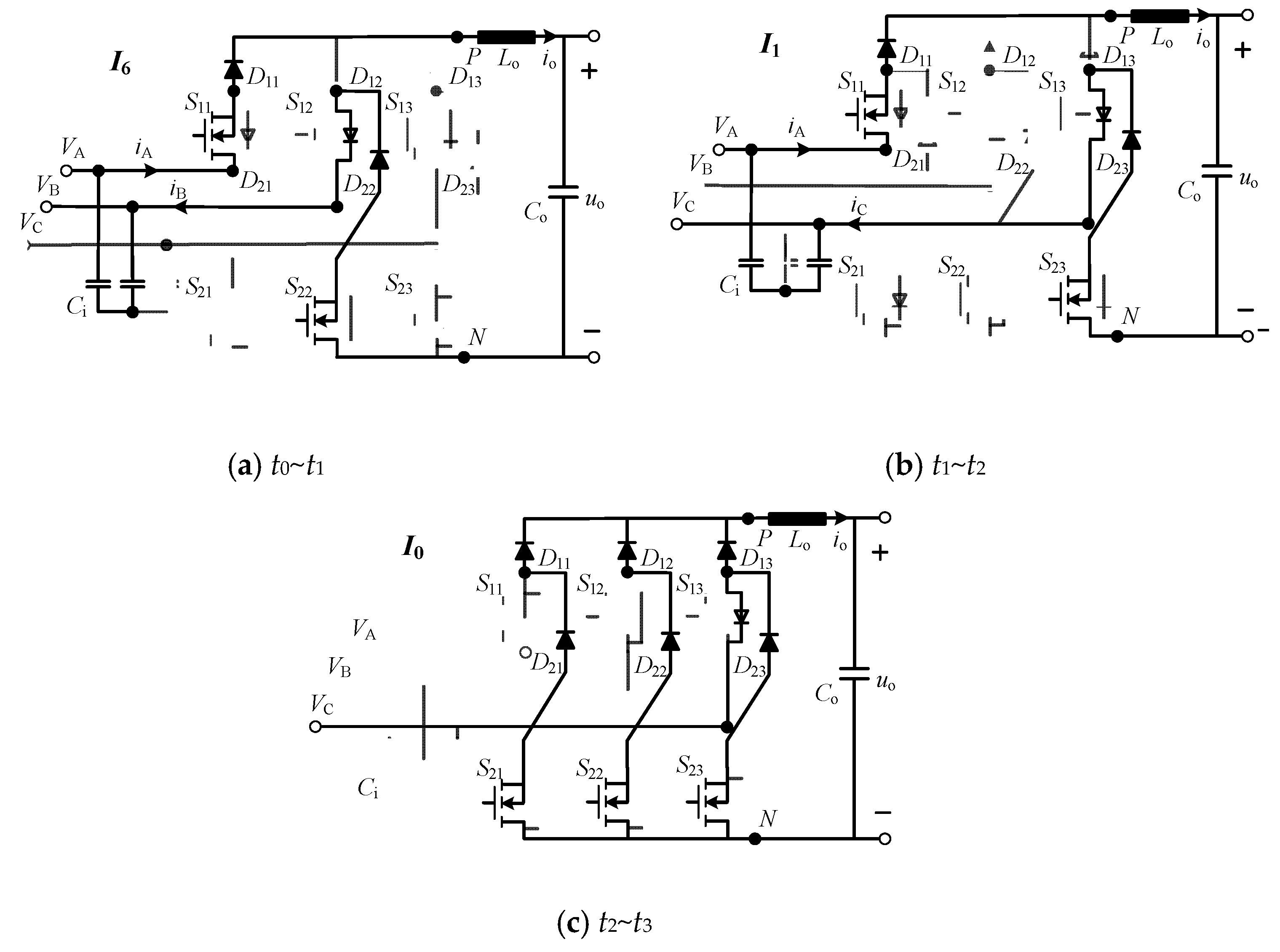
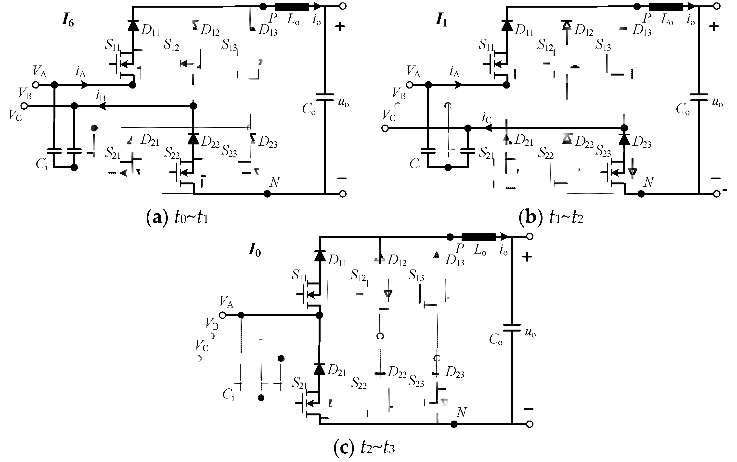
3.2. Operation Modes

With the rapidly increasing switching frequency, the CSRs have been gradually focused on switching loss to improve the converter efficiency. To ensure the minimum number of switching actions in one switching period, Figure 4 shows the switching pattern with three segments in sector I for the proposed CSR. For each segment, Figure 5 shows that the switching states corresponds to different vectors in sector 1.
For the proposed CSR, the complement operation mode in sector 1 during one switching period is divided into three modes. The detailed content is presented as follows:
Mode-1 (t0~t1): At this interval, S11 and S22 are turned on. Due to VA > VB, the diode D12 would remain off, and the body diode of S12 conducts. With the corresponding switching state, the current would flow through S11, D11, S22, D22, and the body diode of S12, resulting in VAB at the output side. The equations during this operation mode are given as:
V P = V A ,   V N = V B ,   i o = i AB
Mode-2 (t1~t2): At this interval, S11 and S23 are turned on. Due to VA > VC, the diode D13 would remain off, and the body diode of S13 conducts. The current would flow through S11, D11, S23, D23, and the body diode of S13, resulting in VAC at the output side. The equations during this operation mode are given as:
V P = V A ,   V N = V C ,   i o = i AC
Mode-3 (t2~t3): At this interval, S21, S22, and S23 are turned on. This is freewheeling mode, and no power transfer happens at the output side. Due to VA > VB > VC, only the body diode of S13 at minimum C phase conducts, the others remain off. The DC current would be shared equally among three paths, and each path consists of two diodes and one transistor. The equations during this operation mode are given as:
V P = V N = V C ,   i o = 1 3 i o + 1 3 i o + 1 3 i o
For the purpose of comparison, Figure 6 shows the switching states of the conventional CSR in sector 1. As can be seen, compared with the conventional CSR, the active vectors in the proposed CSR have the same switching states, while the zero vector will turn on all switches in the lower arm.
The operation modes of the proposed CSR have two differences compared to the conventional one. The first is that a body diode is added in the current path when active vectors act. Another is that three current paths can be obtained in the freewheeling period, and a transistor in each path can be reduced. With the differences from the modified current path, several characteristics could be obtained, especially the low stress on the transistors. Based on the operation modes, the stress on the transistors in the proposed CSR is described in next section.

3.3. Voltage Stress

For the following analysis of the voltage stress, due to the diode conduction characteristics of CSR, summarized in [21], several conclusions are emphasized, as follows:
(1)
Upper arm: If Vx > VP (x = A, B, C), the transistors withstand the voltage stress VxVP, otherwise, the transistors withstand zero voltage stress.
(2)
Lower arm: If Vx > VN (x = A, B, C), the transistors withstand zero voltage stress, otherwise, the transistors withstand the voltage stress VNVx.
Firstly, taking mode 1 (t0~t1) of the proposed CSR in Figure 5a as an example, there will be VP = VA and VN = VB during this time. The transistors in the upper arm both withstand zero voltage stress, while only the transistor S23 in the lower arm would withstand the voltage stress VBVC.
In mode 2 (t1~t2) of Figure 5b, the transistor S23 does not withstand the voltage stress since the transistor turns on at this time, and the others still withstand zero voltage stress.
In mode 3 (t2~t3) of Figure 5c, all the switches in the lower arm turn on, so the corresponding transistors do not withstand voltage stress. Due to VA > VB > VC in sector 1, the bus voltage is the minimum phase voltage VC. Therefore, the transistors S11, S12, and S13 of the upper arm will withstand the voltage stress VAVB, VBVC, and 0, respectively.
Table 2 summarizes the voltage stress of the proposed CSR in sector 1. From the above input voltage analysis in Figure 2, the maximum voltage stress in the upper arm is the input line-to-line voltage amplitude (VAVC)max = VL_im, and the maximum voltage stress in the lower arm would equal half of the input line-to-line voltage amplitude (VBVC)max = VL_im/2. Similarly, the same phenomenon can be found in sector 2 in Table 3.
For the sake of comparative analysis, the voltage stress of the conventional CSR also can be calculated in the same way and is described in Table 2 and Table 3. To compare the voltage stress between the proposed CSR and the conventional CSR more intuitively, taking S11 in the upper arm and S21 in the lower arm as an example, Figure 7 shows the corresponding voltage stress during the entire input cycle. Based on the comparative analysis, it can be seen that half of the transistors for the proposed CSR have lower voltage stress VL_im/2.

3.4. Current Stress

Except for the reduction of voltage stress on the transistors, the proposed CSR has the same function to reduce the current stress due to the asymmetric topological structure and modified modulation strategy. From Figure 8, in the freewheeling mode, the switches of the proposed CSR in the lower arm are all turned on. As expected, three current paths are simultaneously obtained in the proposed CSR system, and each current path only has two diodes and one transistor. Hence, the flowing current for S21~23 is equal to 1/3 of the DC output current. Compared with the conventional CSR, this would cause a significant reduction in current stress. This means that a higher efficiency could be achieved for the proposed CSR when there is a longer freewheeling period at a low modulation index.
A mentioned method that adds a freewheeling diode to the DC side can be commonly used in the CSR circuit. However, the proposed CSR has no additional hardware, and the volume and cost are decreased, so the power density will increase.

4. Discussions

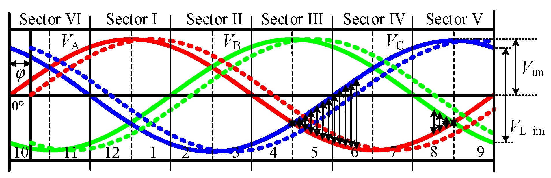
4.1. Influence of Input Displacement Angle

Due to the existence of input filters, the filter capacitor Ci consumes reactive power and an input displacement angle appears between input voltage and current. To solve this problem, the new modulation signals, represented as dotted lines with the compensation angle φ in Figure 9, could be applied to the proposed CSR.
Note that the voltage stress on different transistors would change with the compensation angle. For the transistors in the upper arm, the maximum voltage stress is still input line-to-line voltage amplitude VL_im. However, the voltage stress on the transistors in the lower arm would increase together with the compensation angle. As shown in Figure 9, the maximum voltage stress also reaches VL_im when the compensation angle is set as π/3. It should be noted that the maximum output voltage is achieved at unity power factor operation, so the input displacement angle is always designed as zero to obtain a wide range of output voltage. Therefore, half of the transistors would withstand the voltage stress of nearly VL_im/2 since the input displacement angle is not large in practice.
Considering the input phase voltage amplitude Vim as a boundary, due to VL_im/2 = 0.866 Vim < Vim, there is enough margin, 13.4%, to satisfy the voltage stress change resulting from the input displacement angle. Therefore, it can be concluded that a low voltage rating Vim could be achieved in half of the transistors in the proposed CSR system.

4.2. Power Loss Analysis

The power loss is related to the switching loss Ps and conduction loss Pc. From the operation modes in Figure 5, compared with the conventional CSR, it is clear that a turn-on is added when mode 2 changes to mode 3, and a turn-off is added when mode 3 changes to mode 1 for the proposed CSR. However, the turn-on and turn-off are on low voltage and current stress. Hence, the switching loss of the proposed CSR only has a slight increase compared with the conventional CSR.
Assuming that all semiconductor devices are in a healthy state, the conduction loss Pp, c of the proposed CSR is divided into two types:
{ P p ,   c ,   active   vector = 2 P p ,   c ,   transistor + 3 P p ,   c ,   diode P p ,   c ,   zero   vector = P p ,   c ,   transistor + 2 P p ,   c ,   diode
From Figure 6, the current of the conventional CSR flows through two transistors and two diodes at any time, and the conduction loss Pc, c of the conventional CSR can be expressed in the same form for different vectors:
{ P c ,   c ,   active   vector = 2 P c ,   c ,   transistor + 2 P c ,   c ,   diode P c ,   c ,   zero   vector = 2 P c ,   c ,   transistor + 2 P c ,   c ,   diode
As can be seen in the above equations, compared with the conventional CSR, a body diode is added in the current path when active vectors act, but a transistor is reduced in the current path when the zero vector acts in the proposed CSR system.
Moreover, the conduction loss of a single device is expressed as the sum of two parts:
P c ,   device = i avg V on + i rms 2 R on
where Von is the forward voltage and Ron is the on-resistance.
Since there are three current paths in freewheeling mode in the proposed CSR, the average current iavg and rms current irms have a significant reduction at this time, so the current stress has a greater effect on conduction loss than other factors. In the proposed CSR, although the conduction loss of the active vector is slightly increased with the high number of conduction devices, the conduction loss of the zero vector is significantly reduced due to the lower number of conduction devices and lower current stress in the freewheeling period. It means that the zero vector has an important role for the proposed CSR to reduce conduction loss. On the other hand, the conduction loss of the CSR is much larger than the switching loss in practice [6,33], so the slightly increased switching loss has little effect on total loss when there is a longer period in freewheeling mode.
In summary, compared with the conventional CSR, the proposed CSR has a slightly increased switching loss Ps, and the conduction loss Pc is significantly reduced at a low modulation index. The total loss at a high modulation index is increased slightly but a decreased total loss is achieved at a low modulation index. Therefore, the proposed CSR has a higher efficiency at a low modulation index and it is more suitable for low power applications compared to the conventional CSR.

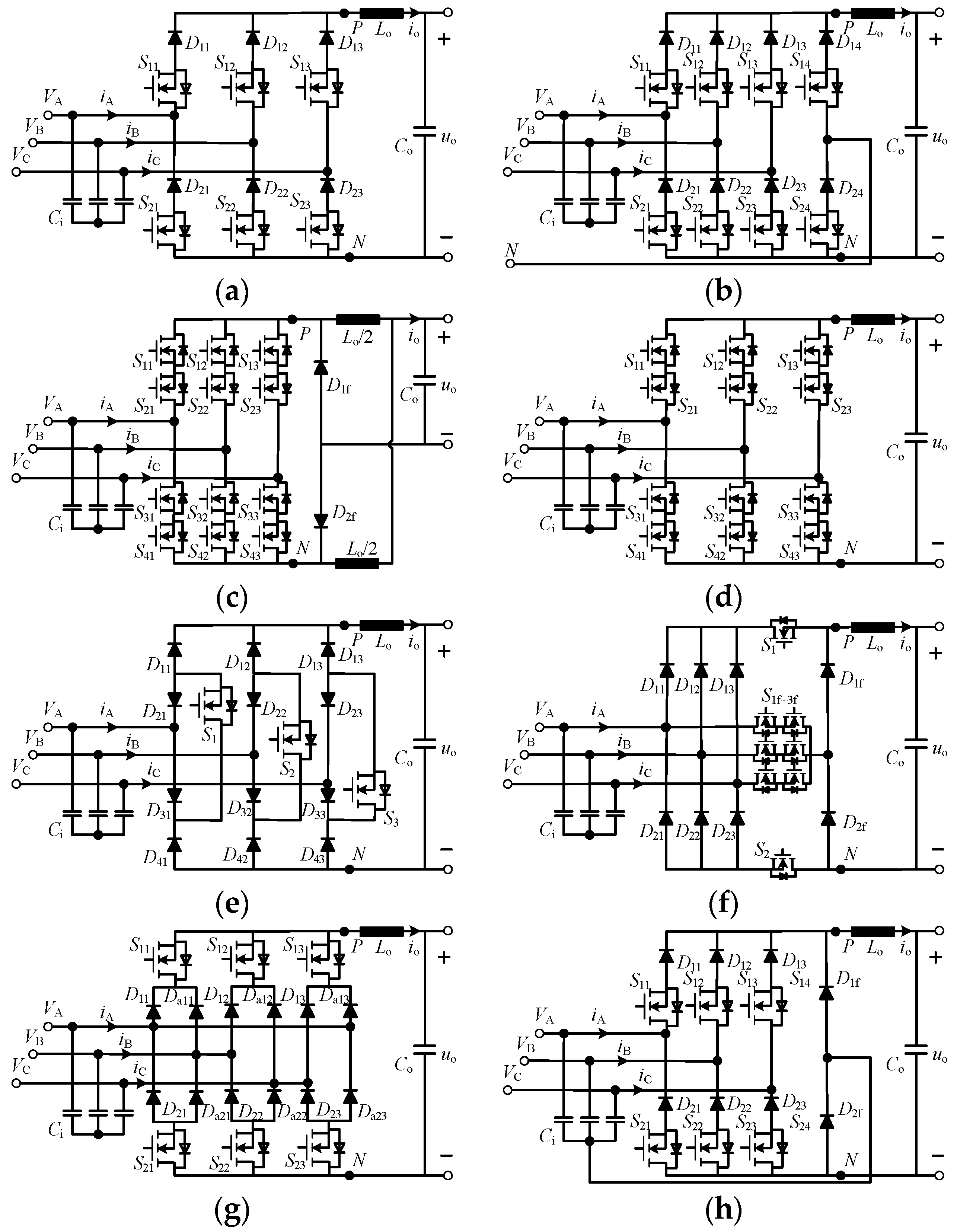
4.3. Comparative Analysis of Other Conventional CSRs

This section presents a brief comparative review of CSRs, including the number of devices, stress on transistors, gain of the converter, PFC function, and other characteristics. Figure 10 summarizes the existing conventional CSR topological structures. Table 4 illustrates the characteristics of the abovementioned conventional CSRs and the proposed CSR.
As can be seen in Figure 10 and Table 4, unlike the current doubler CSR in [16] and matrix-type CSR in [17], a standard six-switch CSR has six transistors and six diodes, as well as the proposed one. Although a three-switch CSR is designed in [18], the converter has the maximum number of diodes and the conduction loss is high. The Swiss-type CSR in [19] can reduce the switching loss, but it also has a higher number of devices and conduction loss. The delta-type CSR in [20] could be used to reduce the conduction loss due to the low current stress, but the effect is significant only at a high modulation index. The Current doubler CSR in [16] also could reduce the conduction loss, but there is a high cost and low gain, and the design of the switching commutation process is more difficult. In addition, all the mentioned CSRs have high voltage stress on transistors. To solve this problem, a CSR with the split-diode connection was introduced in [21]. However, this converter is restricted in applications since it can only operate at unity power factor. Meanwhile, the transistors still withstand the voltage stress Vim rather than 0.866 Vim. For the CSRs, a freewheeling diode on the DC side is the most common method to reduce the conduction loss in the freewheeling period, but the additional hardware could increase costs and reduce power density.
Due to the low current stress in the freewheeling period, half of transistors with a low voltage rating, and no need of additional hardware, the proposed CSR is one of the optimal solutions for high step-down voltage applications.

5. Experimental Result
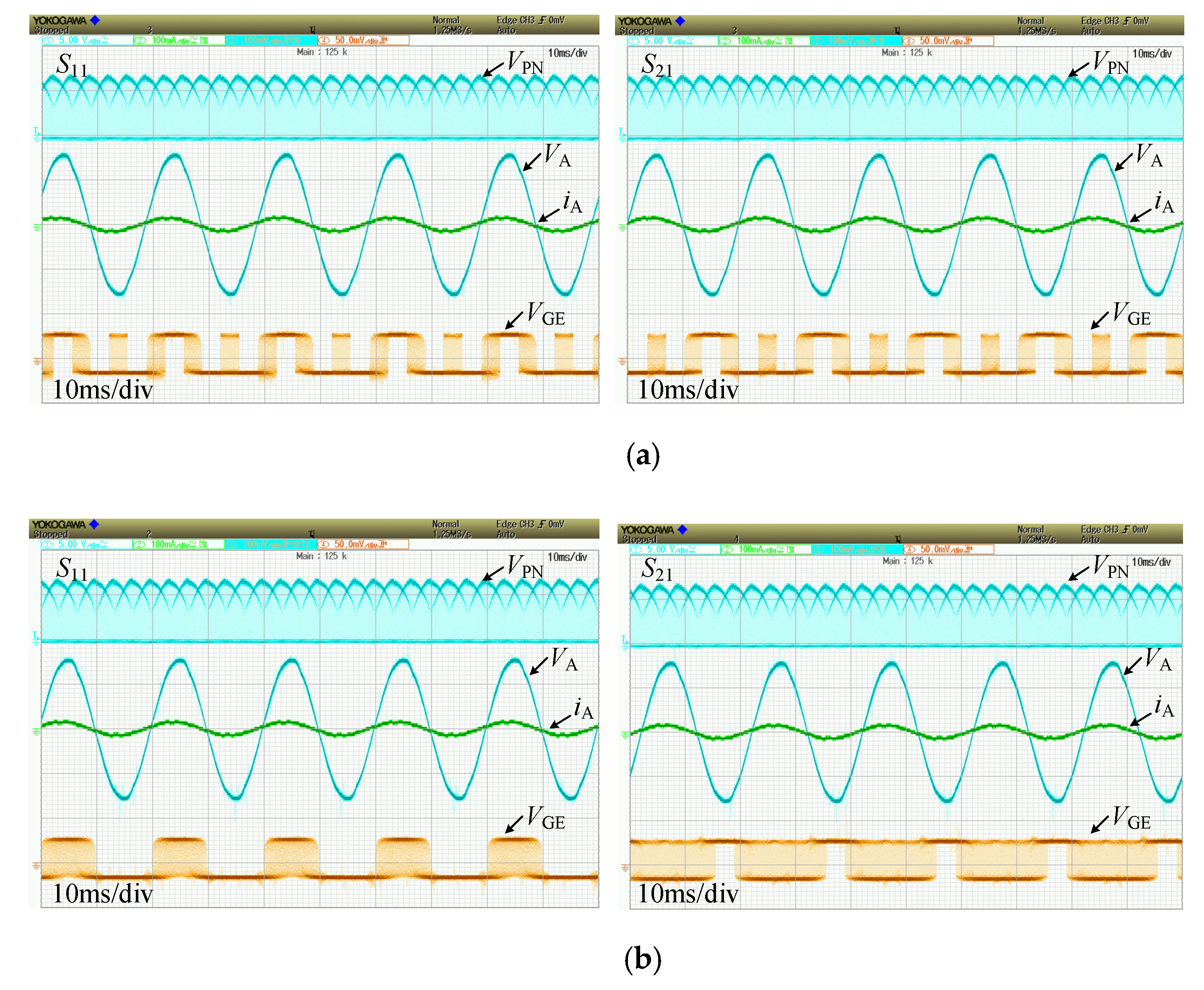
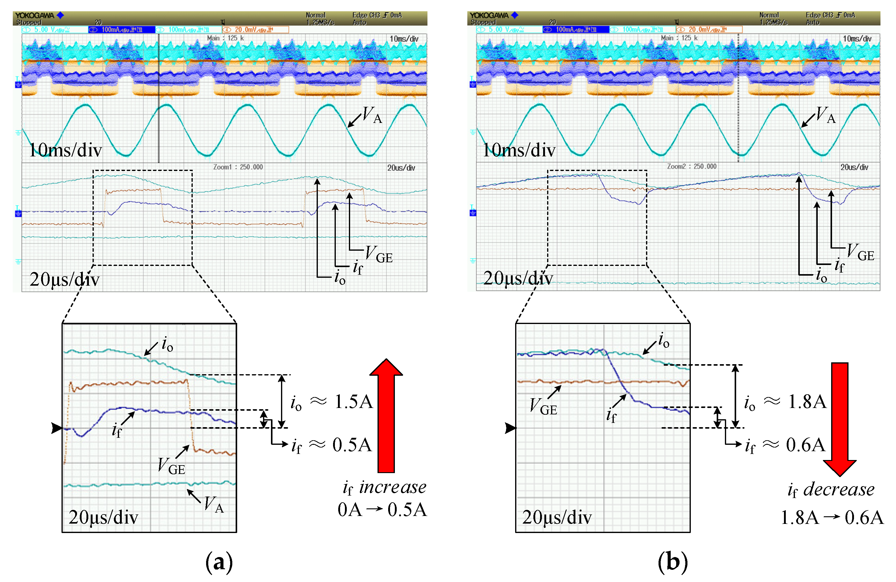
In order to verify the effectiveness of the proposed CSR, comparative experiments between the standard six-switch symmetric CSR and the proposed asymmetric CSR were carried out and the prototype is shown in Figure 11. In particular, the diode–transistor series combination is composed of the IGBT and diode. The input LiCi filter, with a damping resistor Ri, is used to suppress the high-frequency harmonics, and a resistor Ro = 50 Ω serves as the load. Other experimental parameters are summarized in Table 5.

5.1. Voltage Stress

The comparative experimental waveforms between the standard six-switch CSR and the proposed CSR in this paper are shown in Figure 12. Both CSRs could obtain a sinusoidal input current and constant DC output voltage. This means that the proposed CSR has similar input and output characteristics to the conventional CSR. However, there would be a minor displacement angle between the input phase voltage and the current due to the existence of the input filter. This could be solved by a compensation angle that has been mentioned in most of the literature.
In Figure 13a, the voltage stress on all the transistors in the conventional CSR is about VGE = 134 V, which is equal to the line-to-line voltage amplitude VL_im. Additionally, the measured result of the proposed CSR is shown in Figure 13b. Although the transistor S11 in the upper arm still withstands the line-to-line voltage amplitude, the transistor S21 in the lower arm could withstand the voltage stress VGE = 67 V. Hence, half of the transistors in the proposed CSR only need to withstand the voltage stress 1/2 VL_im, which is consistent with the theoretical analysis.

5.2. Unity Power Factor Operation

The input filter could cause a minor displacement angle between the input voltage and the current. In order to operate at unity power factor, a compensation angle should be adopted in the CSR system. The corresponding experimental waveforms under unity power factor operation is shown in Figure 14a. With the compensation angle, the voltage stress has a slight increase in this case. However, the angle is too small in practice, so the voltage stress does not exceed the phase voltage amplitude. Moreover, the total harmonic distortion (THD) of the input current is 2.2%.
The THDs of two CSRs under different modulation indexes are given in Figure 14b. As can be seen, the THDs are quite close in the full modulation range and the values are low in most of the modulation range compared with 5.0% of IEC 61000-3-2. This means that the input performance of the proposed CSR is not affected and is similar to the conventional one. The same input filter could be used in both CSR systems, and the cost and volume of the proposed asymmetrical CSR do not need to change compared with the conventional symmetrical CSR.

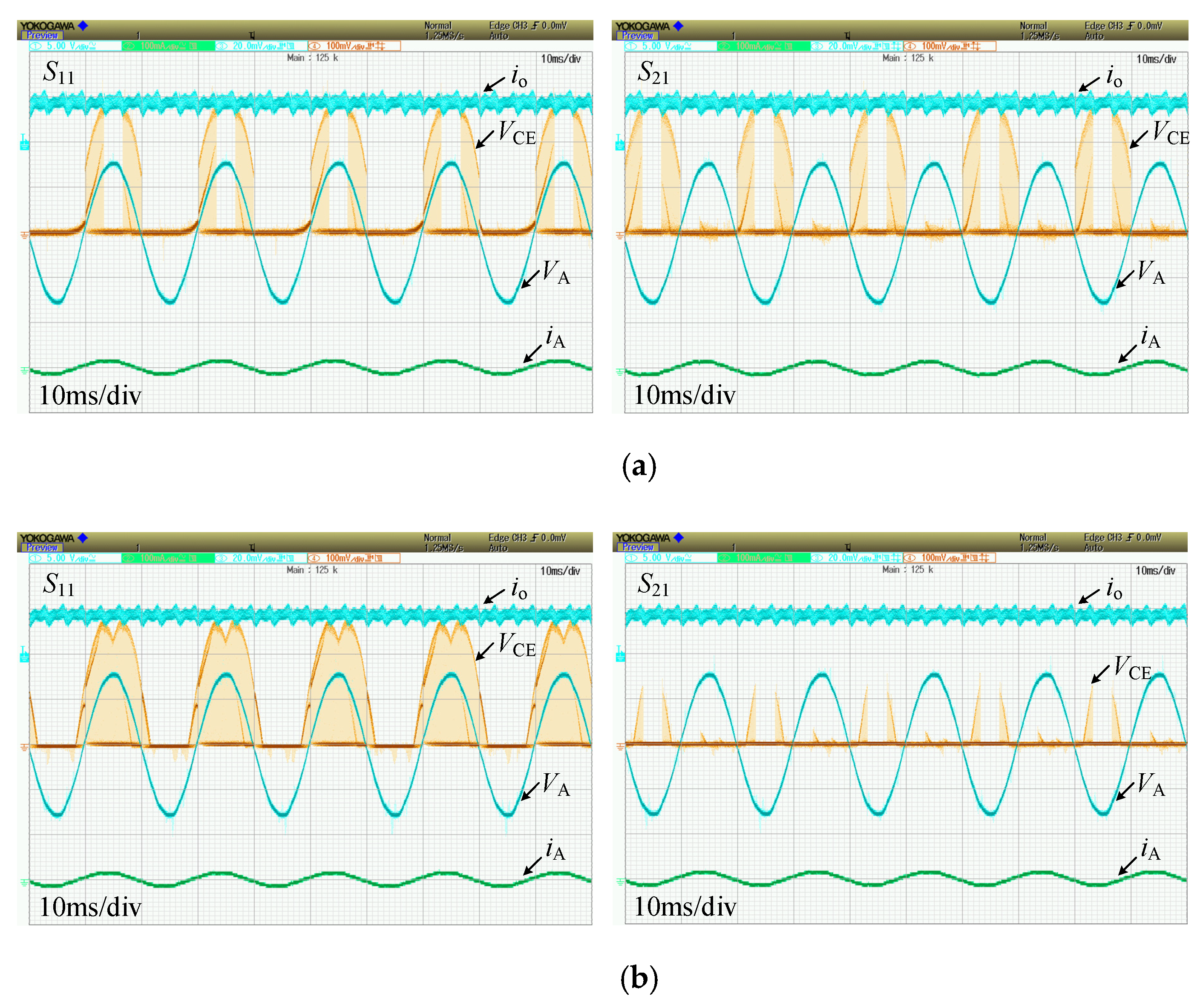
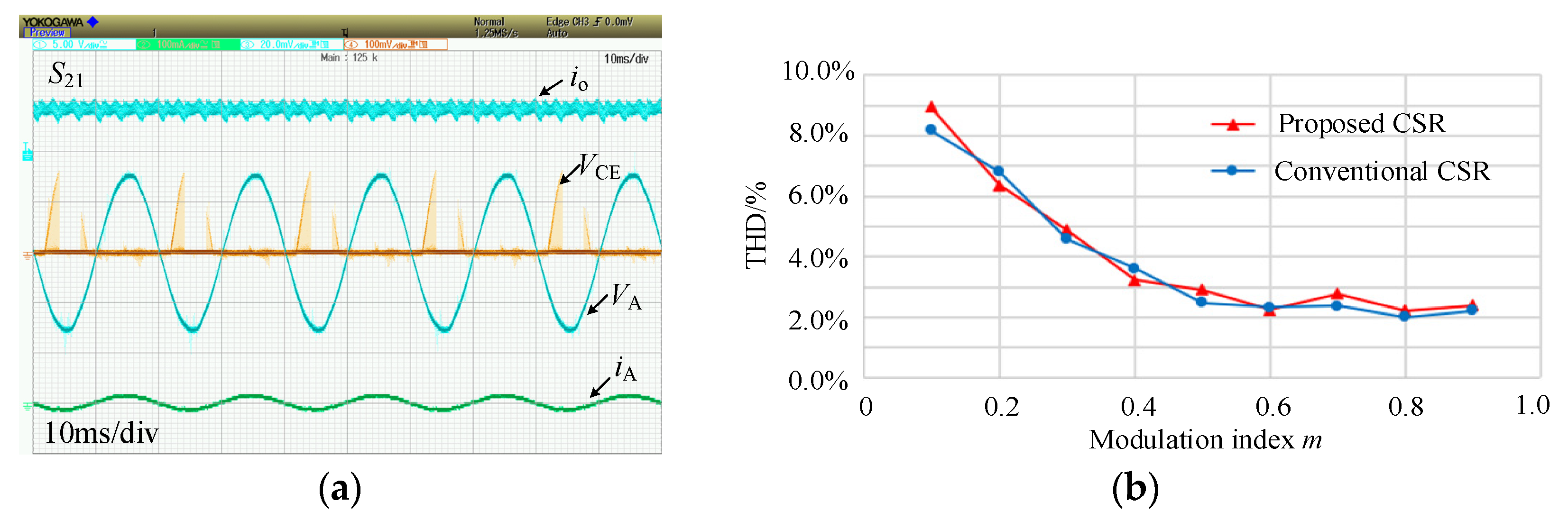
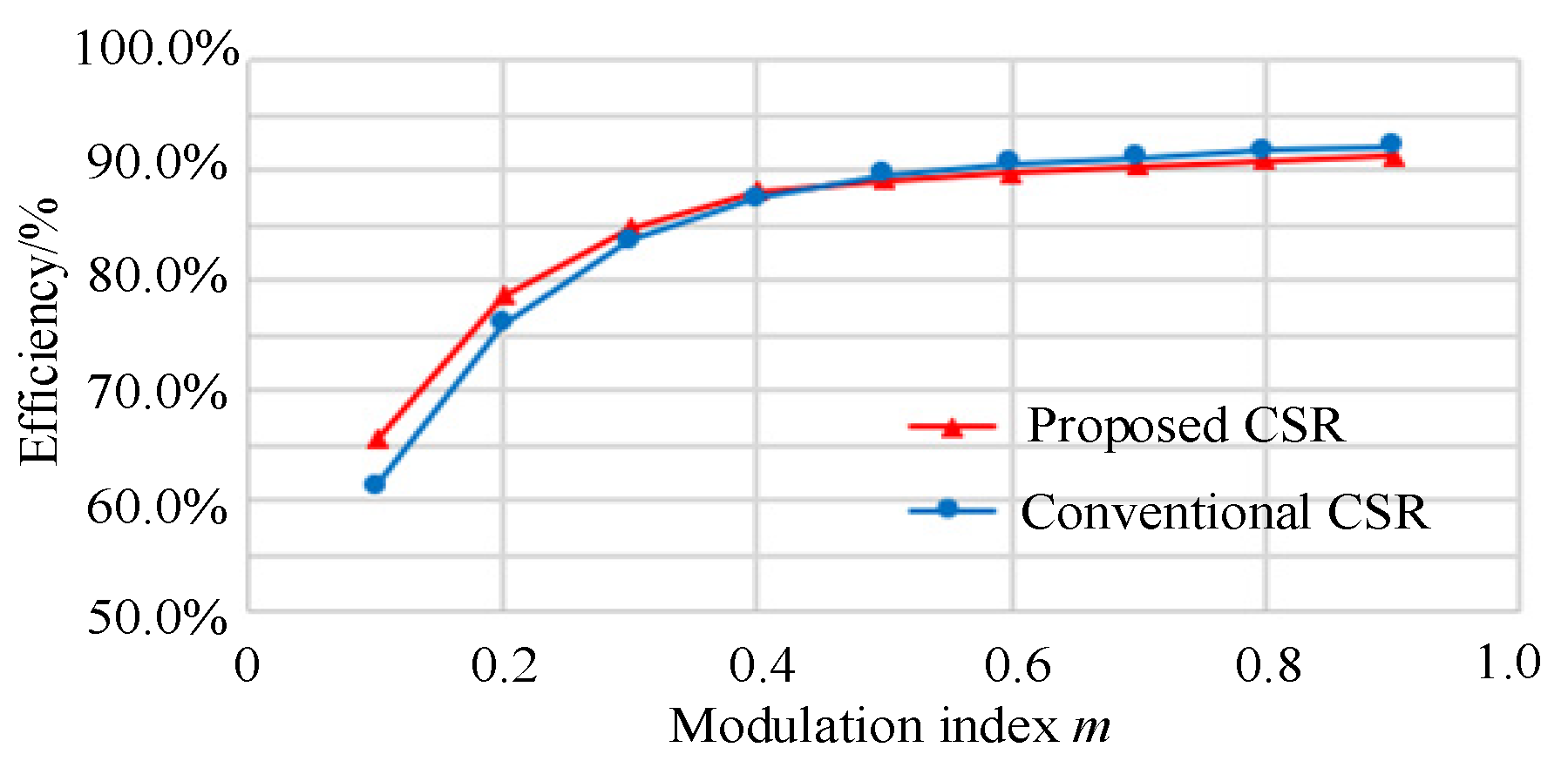
5.3. Current Stress and Efficiency

Figure 15 shows the detailed experimental waveforms of the flowing current for S21. Two zoomed areas would exist, i.e., Figure 15a for sector I and Figure 15b for sector IV. As can be seen, when the zero vector acts, the flowing current if is increased or decreased to nearly 1/3 of the DC output current io in different sectors. The current stress is significantly reduced in freewheeling mode. Due to the reduced current stress, another experimental phenomenon should be emphasized. It can be found that the amplitude of the output current io in Figure 13b is lower than the one in Figure 13a, so a small output filter could be used in the proposed CSR.
The measured efficiency of different CSR systems is illustrated in Figure 16. As expected, with the long freewheeling period, the proposed CSR has a higher efficiency at a low modulation index compared to the conventional CSR.

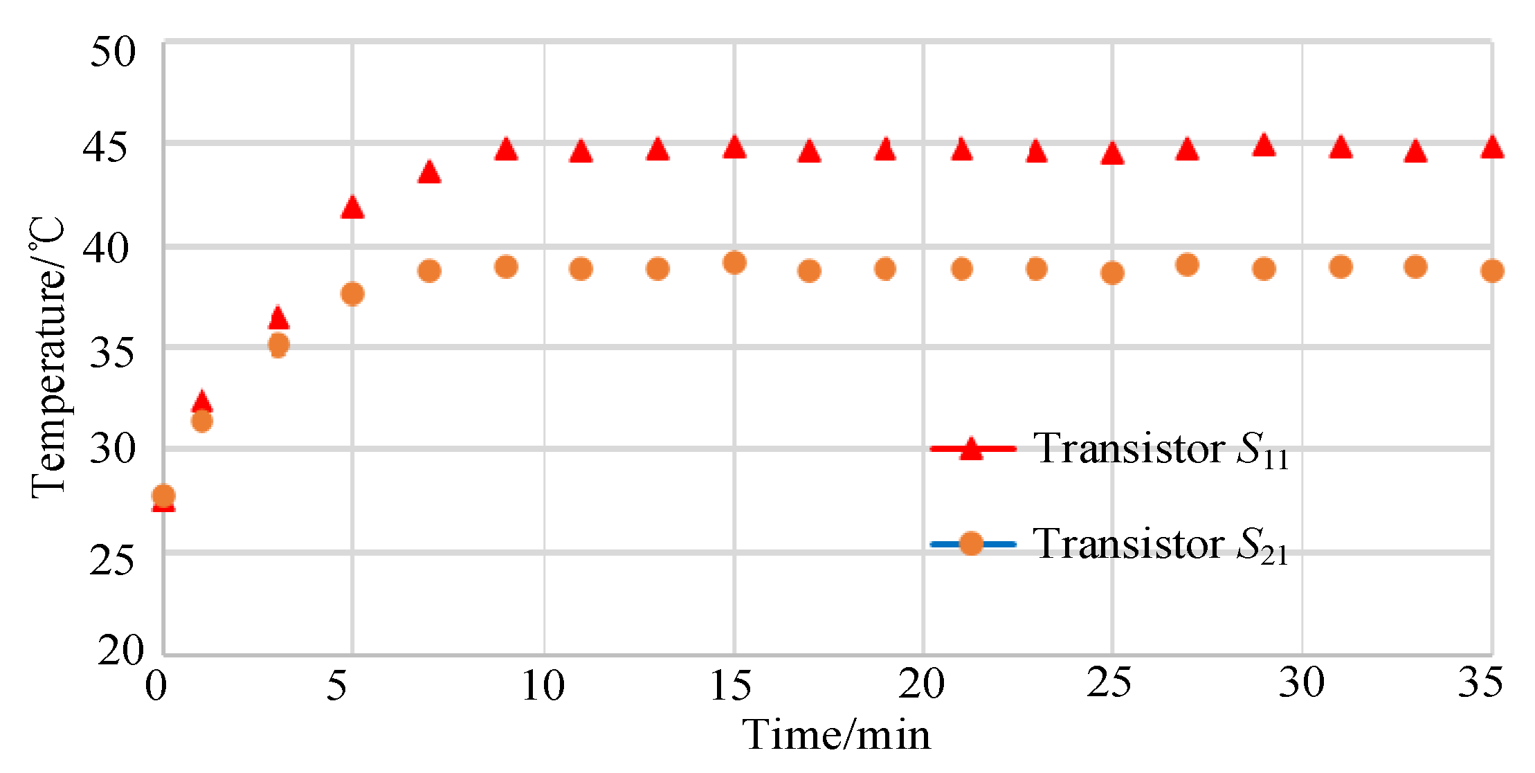
5.4. Temperature Rising

Figure 17 shows the measured temperature of transistor S11 and S21 in the proposed CSR system. Since the current of the proposed CSR could pass through the body diode of transistor S11 in the upper arm, and the transistor S21 in the lower arm withstands low voltage stress. Therefore, the temperature of transistor S11 is a little higher than that of S21, and the heat distribution is uneven for the proposed CSR system. However, all the transistors can be operated in a safe operating area even though the heat dissipating devices are not used in practice. According to the abovementioned experimental results, the system performance of the proposed CSR is not further affected by the inconsistent temperature rise compared to the conventional one.

6. Conclusions

A novel three-phase CSR based on an asymmetrical structure to reduce stress on semiconductor devices is proposed in this paper. Compared with the conventional standard six-switch CSR, the proposed CSR topological structure only has a minor change and no additional hardware is required. With the corresponding SVPWM scheme, half of the transistors could achieve both the lower voltage stress 1/2 VL_im and low current stress 1/3 io in the freewheeling period. Owing to the reduced stress, the proposed CSR has a higher efficiency at a low modulation index, and a smaller output filter could be used in the CSR system. In addition, the CSR was evaluated and compared by an experimental prototype. The comparative experimental results indicate that the proposed CSR has a higher performance in low power output applications. With the reduced stress and low cost, the proposed asymmetrical CSR is a very suitable topology for the implementation of a buck-type power factor correction mains interface, especially for communication power supplies or the integration of fast electric vehicle charging stations within smart grids.

Author Contributions

Conceptualization, W.H. and Z.Z.; methodology, W.H.; software, W.H. and Z.W.; validation, W.H., Z.W. and Z.Z.; writing—original draft preparation, W.H.; writing—review and editing, W.H. and Z.Z.; supervision, Y.X.; project administration, Y.X.; funding acquisition, Y.X. and Z.W. All authors have read and agreed to the published version of the manuscript.

Funding

This research was funded by the Doctoral Program of Dongguan University of Technology under Grant GC300502-11 and the Quality Engineering Project of Dongguan University of Technology under Grant 201802059.

Conflicts of Interest

The authors declare no conflict of interest.

References

  1. Kolar, J.W.; Friedli, T. The Essence of three-phase PFC rectifier systems—Part I. IEEE Trans. Power Electron. 2013, 28, 176–198. [Google Scholar] [CrossRef]
  2. Friedli, T.; Hartmann, M.; Kolar, J.W. The essence of three-phase PFC rectifier systems—Part II. IEEE Trans. Power Electron. 2014, 29, 543–560. [Google Scholar] [CrossRef]
  3. Lee, J.-Y.; Heo, K.-W.; Kim, K.-T.; Jung, J.-H. Analysis and design of three-phase buck rectifier employing ups to supply high reliable DC power. Energies 2020, 13, 1704. [Google Scholar] [CrossRef] [Green Version]
  4. Blecharz, K.; Morawiec, M. Nonlinear control of a doubly fed generator supplied by a current source inverter. Energies 2019, 12, 2235. [Google Scholar] [CrossRef] [Green Version]
  5. Stupar, A.; Friedli, T.; Minibock, J.; Kolar, J.W. Towards a 99% efficient three-phase buck-type PFC rectifier for 400-V DC distribution systems. IEEE Trans. Power Electron. 2012, 27, 1732–1744. [Google Scholar] [CrossRef]
  6. Xu, F.; Guo, B.; Tolbert, L.M.; Leon, M.T.; Fei, W.; Benjamin, B.J. An all-SiC three-phase buck rectifier for high-efficiency data center power supplies. IEEE Trans. Ind. Appl. 2013, 49, 2662–2673. [Google Scholar] [CrossRef]
  7. Xu, F.; Guo, B.; Xu, Z.; Tolbert, L.M.; Fei, W.; Benjamin, B.J. Paralleled Three-Phase Current-Source Rectifiers for High-Efficiency Power Supply Applications. IEEE Trans. Ind. Appl. 2015, 51, 2388–2397. [Google Scholar] [CrossRef]
  8. Yaramasu, V.; Wu, B.; Sen, P.C.; Kouro, S.; Narimani, M. High-power wind energy conversion systems: State-of-the-art and emerging technologies. Proc. IEEE 2015, 103, 740–788. [Google Scholar] [CrossRef]
  9. Kazmierkowski, M.P.; Malesani, L. Current control techniques for three-phase voltage-source PWM converters: A survey. IEEE Trans. Ind. Electron. 1998, 45, 691–703. [Google Scholar] [CrossRef]
  10. Suh, Y.; Steinke, J.K.; Steimer, P.K. Efficiency comparison of voltage-source and current-source drive systems for medium-voltage applications. IEEE Trans. Ind. Electron. 2007, 54, 2521–2531. [Google Scholar] [CrossRef]
  11. Li, Y.; Ding, L.; Li, Y.W. Isomorphic relationships between voltage-source and current-source converters. IEEE Trans. Power Electron. 2020, 34, 7131–7135. [Google Scholar] [CrossRef]
  12. Rodriguez, J.R.; Dixon, J.W.; Espinoza, J.R.; Pontt, J.; Lezana, P. PWM regenerative rectifiers: State of the art. IEEE Trans. Ind. Electron. 2005, 52, 5–22. [Google Scholar] [CrossRef]
  13. Wu, B.; Narimani, M. High-Power Converters and AC Drives; John Wiley & Sons: New York, NY, USA, 2006. [Google Scholar]
  14. Salo, M.; Tuusa, H. A vector controlled current-source PWM rectifier with a novel current damping method. IEEE Trans. Power Electron. 2000, 15, 464–470. [Google Scholar] [CrossRef]
  15. Slazar, L.S.; Zapata, F.H.; Wiechmann, E.F. Analysis, design and experimental evaluation of a four-pole PWM rectifier using space vector modulation. In Proceedings of the 28th Annual IEEE Power Electronics Specialists Conference, Saint Louis, MO, USA, 27 June 1997; Volume 1, pp. 484–490. [Google Scholar]
  16. Singh, A.K.; Jeyasankar, E.; Das, P.; Panda, S.K. A matrix-based nonisolated three-phase AC–DC rectifier with large step-down voltage gain. IEEE Trans. Power Electron. 2017, 32, 4796–4811. [Google Scholar] [CrossRef]
  17. Dang, H.-L.; Jun, E.-S.; Kwak, S. Reduction of DC current ripples by virtual space vector modulation for three-phase AC–DC matrix converters. Energies 2019, 12, 4319. [Google Scholar] [CrossRef] [Green Version]
  18. Nussbaumer, T.; Baumann, M.; Kolar, J.W. Comprehensive design of a three-phase three-switch buck-type PWM rectifier. IEEE Trans. Power Electron. 2007, 22, 551–562. [Google Scholar] [CrossRef]
  19. Soeiro, T.B.; Friedli, T.; Kolar, J.W. Design and implementation of a three-phase buck-type third harmonic current injection PFC rectifier SR. IEEE Trans. Power Electron. 2013, 28, 1608–1621. [Google Scholar] [CrossRef]
  20. Guo, B.; Wang, F.F.; Aeloiza, E. A novel three-phase current source rectifier with delta-type input connection to reduce the device conduction loss. IEEE Trans. Power Electron. 2016, 31, 1074–1084. [Google Scholar] [CrossRef]
  21. Lei, J.; Feng, S.; Zhao, J.; Chen, W.; Wheeler, P.; Shi, M. An improved three-phase buck rectifier topology with reduced voltage stress on transistors. IEEE Trans. Power Electron. 2020, 35, 2458–2466. [Google Scholar] [CrossRef]
  22. Silva, M.; Hensgens, N.; Oliver, J.A.; Alou, P.; García, Ó.; Cobos, J.A. Isolated swiss-forward three-phase rectifier with resonant reset. IEEE Trans. Power Electron. 2016, 31, 4795–4808. [Google Scholar] [CrossRef]
  23. Zhang, B.; Xie, S.; Wang, X.; Xu, J. Modulation method and control strategy for full-bridge-based swiss rectifier to achieve ZVS operation and suppress low-order harmonics of injected current. IEEE Trans. Power Electron. 2020, 35, 6512–6522. [Google Scholar] [CrossRef]
  24. Afsharian, J.; Xu, D.; Wu, B.; Gong, B.; Yang, Z. The optimal PWM modulation and commutation scheme for a three-phase isolated buck matrix-type rectifier. IEEE Trans. Power Electron. 2018, 33, 110–124. [Google Scholar] [CrossRef]
  25. Schrittwieser, L.; Leibl, M.; Kolar, J.W. 99% efficient isolated three-phase matrix-type DAB buck–boost PFC rectifier. IEEE Trans. Power Electron. 2019, 35, 138–157. [Google Scholar] [CrossRef]
  26. Hu, W.; Xie, Y.; Guan, Y.; Wang, Z.; Zhang, Z.; Xu, J. A novel volt-second self-balancing SVPWM scheme to eliminate steady-state DC bias for a three-phase isolated AC-DC matrix converter. IEEE Trans. Power Electron. 2020. [Google Scholar] [CrossRef]
  27. Korkh, O.; Blinov, A.; Vinnikov, D.; Chub, A. Review of isolated matrix inverters: Topologies, modulation methods and applications. Energies 2020, 13, 2394. [Google Scholar] [CrossRef]
  28. Jahdi, S.; Alatise, O.; Bonyadi, R.; Alexakis, P.; Fisher, C.A.; Gonzalez, J.O.; Ran, L.; Mawby, P. An analysis of the switching performance and robustness of power MOSFETs body diodes: A technology evaluation. IEEE Trans. Power Electron. 2015, 30, 2383–2394. [Google Scholar] [CrossRef] [Green Version]
  29. Lin, Z.; Hu, S.; Yuan, Q.; Zhou, X.; Tang, F. Low-reverse recovery charge superjunction MOSFET with a p-type schottky body diode. IEEE Electron. Device Lett. 2017, 38, 1059–1062. [Google Scholar] [CrossRef]
  30. Grbovic, P.J.; Gruson, F.; Idir, N.; Moigne, P.L. Turn-on performance of reverse blocking IGBT (RB IGBT) and optimization using advanced gate driver. IEEE Trans. Power Electron. 2009, 25, 970–980. [Google Scholar] [CrossRef]
  31. Sarnago, H.; Lucia, O.; Mediano, A.; Burdio, J.M. Modulation scheme for improved operation of an RB-IGBT-based resonant inverter applied to domestic induction heating. IEEE Trans. Ind. Electron. 2012, 60, 2066–2073. [Google Scholar] [CrossRef]
  32. Zhou, K.; Huang, L.; Luo, X.; Li, Z.; Li, J.; Dai, G.; Zhang, B. Characterization and performance evaluation of the superjunction RB-IGBT in matrix converter. IEEE Trans. Power Electron. 2017, 33, 3289–3301. [Google Scholar] [CrossRef]
  33. Guo, B.; Wang, F.; Burgos, R.; Aeloiza, E. Modulation scheme analysis for high-efficiency three-phase buck-type rectifier considering different device combinations. IEEE Trans. Power Electron. 2014, 30, 4750–4761. [Google Scholar] [CrossRef]
Figure 1. Topological structure. (a) Conventional current source rectifier (CSR). (b) Proposed CSR.
Energies 13 03331 g001
Figure 2. Three-phase input voltages and sectors.
Energies 13 03331 g002
Figure 3. Space vector pulse width modulation (SVPWM) schematic diagram. (a) Input current vectors and sector partitions. (b) Synthesis of the reference current vector.
Energies 13 03331 g003
Figure 4. Switching patterns in sector I.
Energies 13 03331 g004
Figure 5. Switching states of the proposed CSR in sector 1. (a) Mode 1. (b) Mode 2. (c) Mode 3.
Energies 13 03331 g005
Figure 6. Switching states of the conventional CSR in sector 1. (a) Mode 1. (b) Mode 2. (c) Mode 3.
Energies 13 03331 g006
Figure 7. Comparative schematic diagram of the voltage stress. (a) Conventional CSR. (b) Proposed CSR.
Energies 13 03331 g007
Figure 8. Current stress in the freewheeling mode. (a) Conventional CSR. (b) Proposed CSR.
Energies 13 03331 g008
Figure 9. Voltage stress of S21 with the compensation angle φ.
Energies 13 03331 g009
Figure 10. Topological structures. (a) Six-switch CSR. (b) Three-phase four-wire CSR. (c) Current doubler CSR. (d) Matrix-type CSR. (e) Three-switch CSR. (f) Swiss-type CSR. (g) Delta-type CSR. (h) Split freewheeling diode CSR.
Energies 13 03331 g010
Figure 11. Experimental prototype of the proposed CSR.
Energies 13 03331 g011
Figure 12. Comparative experimental waveforms: input phase voltage VA (50 V/div), input phase current iA (10 A/div), output voltage VPN (100 V/div), and measured drive signals VGE (10 V/div). (a) Conventional standard six-switch CSR. (b) Proposed CSR.
Energies 13 03331 g012
Figure 13. Voltage stress experimental waveforms: input phase voltage VA (50 V/div), input phase current iA (10 A/div), output current io (2 A/div), and measured voltage stress VCE (50 V/div). (a) Conventional standard six-switch CSR. (b) Proposed CSR.
Energies 13 03331 g013
Figure 14. Experimental waveforms under unity power factor: input phase voltage VA (50 V/div), input phase current iA (10 A/div), output current io (2 A/div), and measured voltage stress VCE (50 V/div). (a) Voltage stress. (b) Total harmonic distortion (THD) of input current.
Energies 13 03331 g014
Figure 15. Flowing current of S21: input phase voltage VA (50 V/div), output current io (1 A/div), flowing current if (1 A/div), and measured drive signals VGE (10 V/div). (a) Detailed flowing current in Section 1. (b) Detailed flowing current in Section 4.
Energies 13 03331 g015
Figure 16. Efficiency comparison of different CSRs.
Energies 13 03331 g016
Figure 17. Temperature rising of transistors S11 and S21 in the proposed CSR system.
Energies 13 03331 g017
Table 1. The switching states corresponding to the space vectors of the proposed CSR.
VectorsUpper ArmLower ArmVPNiAiBiC
S11S12S13S21S22S23
Active
vectors
I1××××VACio0io
I2××××VBC0ioio
I3××××VBAioio0
I4××××VCAio0io
I5××××VCB0ioio
I6××××VABioio0
Zero
vector
I0×××0000
Table 2. Voltage stress of different CSRs in sector 1.
Conventional CSRProposed CSR
Mode 1Mode 2Mode 3Mode 1Mode 2Mode 3
Upper
arm
S1100000VAVC
S1200000VBVC
S13000000
Lower
arm
S21000000
S2200VAVB000
S23VBVC0VAVCVBVC00
Table 3. Voltage stress of different CSRs in sector 2.
Conventional CSRProposed CSR
Mode 1Mode 2Mode 3Mode 1Mode 2Mode 3
Upper
arm
S110VAVBVAVC0VAVBVAVC
S1200VBVC00VBVC
S13000000
Lower
arm
S21000000
S22000000
S23000000
Table 4. Comparative analysis of the CSRs.
Number of DevicesStress on TransistorsGainPFC
TransistorDiodeCurrentVoltage
Proposed66LowLow1.5 VimYes
Six-switch [14]66HighHigh1.5 VimYes
Four-wire [15]88HighHigh1.5 VimYes
Current doubler [16]122LowHigh0.75 VimYes
Matrix-type [17]120HighHigh1.5 VimYes
Three-switch [18]312HighHigh1.5 VimYes
Swiss-type [19]88HighHigh1.5 VimYes
Delta-type [20]612LowHigh1.5 VimYes
Split diode [21]68HighMedium1.5 VimNO
Table 5. Parameters of the experimental prototype.
ParameterSymbolValue/Types
Input voltageVrms55 V
Input frequencyfg50 Hz
Input filter resistorRi5 Ω
Input filter inductorLi380 µH
Input filter capacitorCi10 µF
Output filter inductorLo2.5 mH
Output filter capacitorCo33 µF
Switching frequencyfs10 kHz
Modulation indexm0.8
Output powerPo200 W
TransistorsS11S23FGA25N120
DiodesD11D23RHRG30120
Control circuitDSP + FPGATMS320F28335/
CoreEP4CE6d

