Article

Modular Isolated DC-DC Converters for Ultra-Fast EV Chargers: A Generalized Modeling and Control Approach †

Department of Electrical Engineering, Qatar University, Doha 2713, Qatar
*
Author to whom correspondence should be addressed.
This paper is an extended version of our paper published in 2019 2nd International Conference on Smart Grid and Renewable Energy (SGRE), Doha, Qatar, 19–21 November 2019; pp. 1–6.
Energies 2020, 13(10), 2540; https://doi.org/10.3390/en13102540
Submission received: 5 April 2020 / Revised: 13 May 2020 / Accepted: 14 May 2020 / Published: 17 May 2020
(This article belongs to the Special Issue Electric Systems for Transportation)

Abstract

:
Electric Vehicles (EVs) play a significant role in the reduction of CO2 emissions and other health-threatening air pollutants Accordingly, several research studies are introduced owing to replacing conventional gasoline-powered vehicles with battery-powered EVs. However, the ultra-fast charging (UFC) of the battery pack or the rapid recharging of the battery requires specific demands, including both: the EV battery and the influence on the power grid. In this regard, advanced power electronics technologies are emerging significantly to replace the currently existing gas station infrastructures with the EV charging stations to move from conventional charging (range of hours) to UFC (range of minutes). Among these power electronics conversion systems, the DC-DC conversion stage plays an essential role in supplying energy to the EV via charging the EV’s battery. Accordingly, this paper aims to present possible architectures of connecting multiple Dual Active Bridge (DAB) units as the DC-DC stage of the EV fast charger and study their Small-Signal Modeling (SSM) and their control scheme. These are, namely, Input-Series Output-Series (ISOS), Input-Series Output-Parallel (ISOP), Input-Parallel Output-Parallel (IPOP), and Input-Parallel Output-Series (IPOS). The control scheme for each system is studied through controlling the output filter inductor current such that the current profile is based on Reflex Charging (RC). The main contribution of this paper can be highlighted in providing generalized SSM as well as providing a generalized control approach for the Input-Series Input-Parallel Output-Series Output-Parallel (ISIP-OSOP) connection. The generalized model is verified with three different architectures. The control strategy for each architecture is studied to ensure equal power sharing, where simulation results are provided to elucidate the presented concept considering a three-module ISOS, IPOP, ISOP, and IPOS DC-DC converters.

1. Introduction

Due to high fossil fuel prices, CO2 emissions and other health-threatening emissions, environmental awareness has shown a high interest in Electric Vehicles (EVs) [1]. Replacing conventional gasoline-powered vehicles with battery-powered EVs is expected to reduce fuel consumption significantly [2]. As a response to the ecological issues, a movement towards electrification is taking place in the transport sector. Many research studies have been provided to support this movement in [3,4,5,6]. To compete with conventional combustion engine vehicles and ensure the wide adoption of EVs, significant efforts are still needed. One of the main issues limiting the widespread penetration of EVs is the long charging duration that usually exceeds 30 min [7]. In other words, one of the challenging problems limiting EVs’ utilization is the lack of efficient and fast charging capabilities. Accordingly, Ultra-Fast Charging (UFC) is a necessary concept to be investigated to allow massive integration for EVs in the market, particularly when concerning long-distance travel [2]. In this regard, industrial and academic fields have been pushed to explore the Ultra-Fast EV Charging (UF-EVC) concept. This is due to the fact that fast-charging stations allow the recharging process to be done in a few minutes and hence overcoming EVs limitation problem. Studies have shown that the charging process affects EVs’ adoption significantly. Therefore, future EV charging stations should have the capability of charging EVs from 10% State-of-Charge (SoC) to 90 % SoC in few minutes [8,9,10]. Nowadays, battery technologies are evolving, enabling the EV’s battery to be charged at higher power levels. Currently, offboard fast-charging stations are provided to speed up the charging process [10,11,12,13,14].
Conventionally, the charging methods are categorized based on the charging speed and power into three different levels, which are: level 1, level 2, and level 3 (also termed as the DC fast charging) [15]. Shortly, a new battery technology that reduces the charging time to 3 min is expected to be commercialized [15]. This introduces a new charging level termed the ultra-fast/super-fast charging level, which is different from the present DC fast charging that is commonly used in industrial and academic fields 15. Table 1 shows the electrical specifications for the EV charging stations [15].
To enable UFC for EVs, advanced power electronics converter technologies play an essential role in terms of both flexibility and efficiency. Accordingly, this paper focuses on high-power DC-DC converters that can be employed in UFC stations. As mentioned earlier, one of the main obstacles limiting the broad adoption of EVs is the long charging time. To avoid this problem, UFCs should be designed at a higher power level. Toward this direction, BMW and Porsche, as a part of the Fast Charge Consortium (a group of industrial companies engaged in the “Fast Charge” research project), have demonstrated the latest super-fast EV charger that can considerably charge EVs faster than the present charging methods [16]. Similar systems are demoed by the two companies, where the electric prototype for Porsche is capable of charging at a power level of 400   kW in less than 3 min for the first 100   km with a battery capacity of 90   kWh . While the experimental system for BMW is capable of charging at a power level of 350   kW in 15 min ( 10 % to 80 % SoC) [16]. The charging process is done using a DC-DC converter that converts a charging station input voltage of 800   V to a lower voltage of 400   V [17]. The latest prototypes by both companies can work up to 900 and 500   A , meaning that it can charge at a power level of 450   kW , which is three to nine times the capacity of the existing up-to-date DC fast-charging stations [16,17]. This capacity increase significantly reduces the duration of the charging time. Tesla has shown significant efforts to introduce fast charging for EVs. However, the current cars presented by Tesla can only charge at a maximum of 120   kW . Tesla will add enhanced superchargers in 2020. Nonetheless, the charging speed of those cars is boosted to double the charging rate of the current vehicles [16].
The Fast Charge research group is investigating the required technical specifications in terms of the fast charging infrastructure and the EV to match the high charging capacities. Siemens, as a part of the research group, has provided an energy supply system to be used in the project, allowing researchers to examine the fast-charging capacity limits demonstrated by the EV’s batteries. The system can handle high voltage that reaches up to 920   V , which is the voltage level predicted for the future EVs [17]. The controller of the charger makes sure that the output is modified automatically according to the EV, allowing different EVs to be charged using a single infrastructure. To illustrate, the UFC station can be used with battery systems rated at 400 and 800   V , where the charging capacity is adapted automatically to the maximum charging capacity on the EV side. The system is characterized by its flexibility and modularity, allowing multiple EVs to be charged at the same time instant [17].
Such fast-charging stations require DC-DC converters of high-power to be designed to achieve high reliability and high efficiency for the system. One of the fast-charging stations’ requirements is to develop the DC-DC converters in a modular structure since such configuration can provide redundancy, easier maintenance, as well as scalability, and ride-through capability [18].
To further illustrate, to meet the requirements of the high-voltage high-power fast charger, two approaches are established. The first approach is through semiconductor devices with high-voltage and high-current ratings to be integrated into the two-level converter topologies with series/parallel connections. However, the series connection of power switches results in the unsymmetrical sharing of voltage among the switching devices because of the switches’ unequal parameters, such as the switching delays, leakage inductance, and collector-to-emitter capacitance. Accordingly, voltage balancing methods are required to avoid any failure [19].
In the second approach, power electronic converters are usually pursued to be built in a modular manner in fast-charging stations [20]. Modular converters contain several numbers of smaller modules. Building converters in a modular way is a cost-effective solution. Besides, smaller modules can be hot swapped in failure cases, which makes the maintenance of such converters easier. Moreover, the number of modules can be scaled up according to the power rating of the system.
Furthermore, by installing more modules, the concept of redundancy can be established. In other words, in modular structure-based DC-DC converters, each cell handles a small portion of the total input power. Consequently, the selected power switches are of lower voltage ratings, hence, higher switching frequency capability. Therefore, the converter efficiency is improved due to lower losses, and the transformer size is reduced due to the increase in the switching frequency [21,22]. To avoid the demerits associated with the first approach, modular converters’ topologies, such as Multimodule Converters and Modular Multilevel Converters, are used to provide the modularity feature and achieve high-voltage and high-power requirements [23]. Nonetheless, the multimodule DC-DC converters are considered in this paper since the modularity concept is not limited only to the power electronics but also is extended to include the magnetics. Moreover, higher switching frequencies can be achieved in the AC link, which results in reduced weight and size of the overall power converter. Although the high-frequency transformer employment allows for a reduction in the overall converter size and weight, the overall system cost is increased, especially with the power increase. Multimodule converters are applicable for EV UFC since scalability, reliability, redundancy, and ride-through capability can be provided. Besides, such converters utilize low-power modules where each module handles only a fraction of the total required power. However, the system complexity increases with the increase in the number of modules. Moreover, the impact of EVs UFC on the grid should be considered. Therefore, coordinated charging should be devised to address challenges that might be encountered with uncoordinated EVs UFC, particularly when multiple batteries are charged through UFC mode. Furthermore, the on-going technology development in the batteries’ industry supports the proliferation of EVs UFC through introducing high capacity batteries that can accept such mode of charging.
Multimodule DC-DC converters can offer a bidirectional power flow through utilizing submodules that contain Dual Active Bridge (DAB), Dual Half Bridge (DHB), or series resonant converters, where each configuration has its pros and cons [24,25]. In multimodule converters, soft switching operation, as well as higher switching frequency, can be achieved, resulting in a significant reduction in the component volume without sacrificing the efficiency [24]. The possible architectures of connecting multimodule-based DAB units are classified into four main categories, which are: Input-Series Output-Series (ISOS), Input-Parallel Output-Parallel (IPOP), Input-Series Output-Parallel (ISOP), Input-Parallel Output-Series (IPOS) [26].
A typical fast charger is usually connected to a 400   V AC grid ( 570   V D C rectified) [27]. However, this low voltage results in high current and causes high losses in the magnetic components, bus bars, and switching devices [28]. Accordingly, connecting the fast charger to a higher input voltage level ( 10 40   kV ) will reduce the current and conduction losses in the DC-DC converter. In [29,30], a DC link with a voltage of 1000   V has been proposed to the high power, while, in [31], the fast charger is connected to a medium voltage connection of 2.4   kV . In [28], a multiport converter for EVs’ fast chargers has been proposed, where the charging process is done via a 6 to 10   kV supply grid.
In [15], a power architecture for the upcoming super-fast EV charging stations has been proposed. The presented architecture in [15], is interfaced with a medium voltage grid with a voltage level of 4.8   kV . It supports the grid functionality since it can allow bidirectional power flow and can reduce during the EV charging the conduction energy loss of the grid. However, in [7], DC-DC converters for high-power EV UFC stations have been presented. The semiconductor devices voltage ratings are reduced through splitting the DC input voltage. In addition, a modulation scheme named triangular current modulation is applied to achieve Zero Voltage Switching for all the switching devices. This accordingly increases the efficiency of the system. The converter in [7] can achieve an efficiency of 99.5 % . To reduce the ripple content of the output current and achieve a high power density, multiple modules are parallel interleaved. In [2], reactive power operation is investigated using an offboard charging station. In [32], two different converter architectures for UF-EVC stations are presented. The first architecture is based on low-frequency isolation (non-isolated DC-DC converter), while the second approach is based on high-frequency isolation (galvanic isolated DC-DC converter). Technical evaluation for the two architectures is carried out where the pros and cons of each topology are highlighted. Besides, simulation results elaborating on the impact of the DC fast charging station on the grid are also provided in [32]. In [1], to realize medium-voltage UF-EVC stations, a multiport power converter has been proposed. A cascaded H-bridge is utilized at the grid side. Besides, to reduce the charging station effect on the grid, the battery energy storage elements are integrated in a split manner on the level of each submodule. Talking about the DC-DC conversion stage presented in [1], multiple Dual Half Bridge units are connected in parallel, where the multiport concept at the output side is achieved by selecting different submodule configurations. This is done to charge multiple EVs at the same time instant without the need for extra chargers. Operation modes, as well as the control techniques, have been addressed in [1].
In [33], a Full-Bridge Phase-Shifted DC-DC converter that combines the features of the double inductor rectifier and the conventional hybrid switching converter has been proposed for EV DC fast chargers. The principle of operation, as well as the characteristics and design specifications, are provided. The presented DC-DC converter in [33], can achieve both: zero voltage switching and zero current switching in the leading and the lagging legs, respectively. In [31], a medium-voltage high-power isolated DC-DC converter for EVs fast chargers have been presented. The employed DC-DC converter is a modular-based structure utilizing silicon carbide switching devices to convert a single-phase rectified input voltage of 2.4   kV to a variable DC output. It is a unidirectional converter that is connected in series from the input side and connected in parallel from the output side.
In [34], the AC-DC and DC-DC stages of an EV charger have been studied. The DC-DC stage utilizes interleaved DC-DC converters to be connected to a high-voltage network ( 13.8   kV ) . The interleaved DC-DC converters are accompanied with several advantages that can be highlighted in lower input ripple and lower inductors cost and size. The charger presented in [34] allows for bidirectional power flow so that it can support renewable energy sources and smart grid applications. It is suitable for a high-power fast charger of 400   kW with an EV battery with a rated voltage level of 500   V . However, in [35], a fast charger that is based on a single stage has been proposed. In other words, the power factor correction and zero voltage switching are achieved in one single AC-DC stage. The charger utilizes DAB units that are connected in series and parallel at the input and output sides, respectively. The use of one stage resulted in the DC link capacitor elimination, allowing for higher efficiency and higher power density to be achieved. In [18], a fast-charging system for EVs is proposed. The system consists of a 15   kW multimodule converter that utilizes a three-phase rectifier and a Full-Bridge DC-DC converter. Multiple units are used in a modular manner and connected in parallel at the input side and series or parallel at the output side. To clarify, modules are connected in IPOS to provide a higher voltage that reaches up to ( 1000   V ) or connected in IPOP to provide higher output current at a voltage level of ( 500   V ) .
In [36], a power converter that interfaces a three-phase medium-voltage grid with EV batteries has been proposed. The AC-DC stage utilizes a cascaded H-Bridge converter, in which the battery energy storage systems are integrated in a split manner to reduce the effect of the charging station on the grid. Modular DC-DC converters utilizing the Full-Bridge Phase-Shifted topology are employed to charge the EV battery. The DC-DC converters are connected in parallel to provide high currents.
According to the latest technical specifications for fast charging stations, the charging process can be done through a 400   VAC or it can be done through a medium voltage grid supply that ranges from 10 to 40   kV to avoid high current and high losses. Assuming a fast charger rated at 350   kW and EV battery rated at a high voltage level ( 400 920   V ) . Different scenarios of the mentioned specifications result in the four different architectures of the multimodule DC-DC converters, which are ISOS, IPOP, ISOP, and IPOS. In this paper, these scenarios are discussed along with the control strategy for each architecture. To support the power converter controller design, the Small-Signal Model (SSM) for the four architectures is studied in detail. Moreover, to ensure equal power sharing among the employed modules, the control scheme for the four architectures is investigated. Moreover, a generalized SSM for any multimodule DC-DC converters’ connection, including Input-Series Input-Parallel Output-Series Output-Parallel (ISIP-OSOP), is provided. This is achieved by studying the SSM of Full-Bridge Phase-Shift (FB-PS) DC-DC converter, two-module IPOS, three-module ISOP, and four-module Input-Series Input-Parallel Output-Series (ISIPOS) presented in [37,38,39,40,41,42], respectively. After deriving the generalized model, the model is verified with the multimodule configurations presented in [38,39,40,41,42].
The main contribution of the paper can be summarized as follows:
  • A generalized model for the multimodule ISIP-OSOP DC-DC converter is provided. It is worth mentioning that the work presented in [40] is extended to include the SSM as well as the control schemes for the three other multimodule configurations, which are ISOS, IPOP, and IPOS. In addition to a generalized SSM applicable for all the basic architectures for multimodule DC-DC converters.
  • Detailed SSM for the four architectures of the multimodule converter, which are ISOS, ISOP, IPOP, and IPOS, is provided in detail.
  • The control strategy to guarantee uniform power distribution among the modules is studied. The strategies are based on current control Reflex Charging (RC) considering high-power-level UFC stations.
This paper is organized such that: Section 2 presents the ISOS circuit configuration as well as the ISOS SSM. Section 3 presents the ISOP multimodule DC-DC converter referring to the work that has been previously published in [40]. Section 4 and Section 5 provide the circuit configuration and SSM for the IPOP and IPOS DC-DC converter, respectively. Section 6 addresses the generalized SSM for the ISIP-OSOP multimodule DC-DC converter along with its verification. Section 7 provides the control scheme for the four architectures to achieve equal power sharing among the employed modules. Finally, Section 8 presents the conclusion.

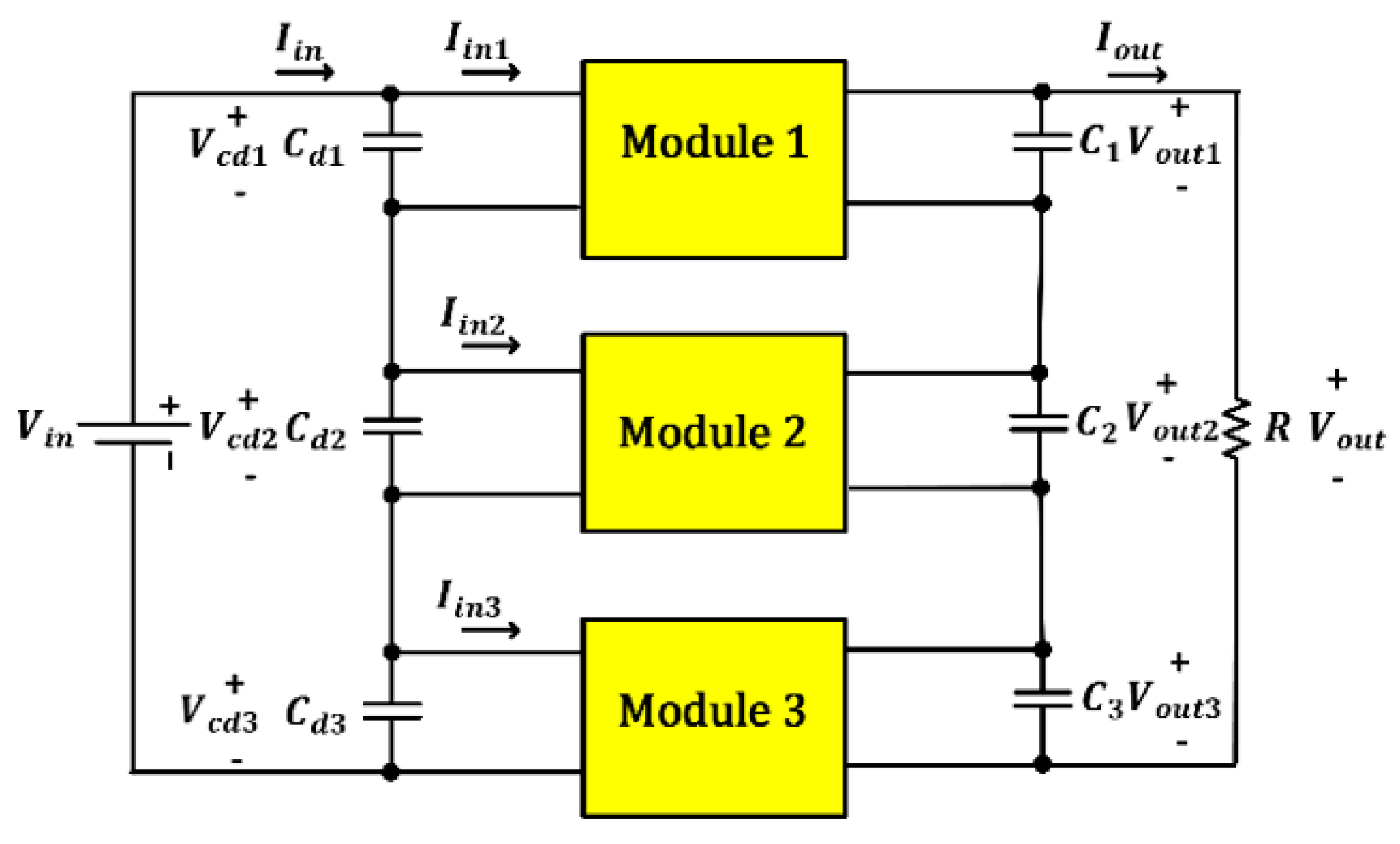
2. Input-Series Output-Series (ISOS) DC-DC Converter

In this section, the ISOS DC-DC converter circuit diagram, as well as the ISOS DC-DC converter SSM, are discussed in detail. The analysis carried out in this section, as well as the following sections, is not restricted to unidirectional power flow and can be applied for bidirectional power flow. In addition, a three-module based DAB topology is considered. Such configurations are employed when galvanic isolation is required.
To reduce the SSM in terms of complexity, it is assumed that all the modules of the ISOS, ISOP, IPOP, and IPOS DC-DC converter have an equal turns ratio and effective duty cycle as well as the same inductor and capacitor values. In other words, the SSM for the four architectures is derived, assuming ideal conditions. The SSM, carried out in this section and the following sections, is used in Section 7 to support the controller design for each configuration.

2.1. ISOS Circuit Diagram

An ISOS DC-DC converter is employed in high input voltage and high output voltage applications [43]. The ISOS converter configuration is shown in Figure 1, where modules are connected in series at the input and the output sides. The ISOS DC-DC converter shown in Figure 1 is needed for a high step-up ratio. This configuration is employed in high-voltage applications where neither the input side voltage nor the output side voltage is within the semiconductor devices voltage ratings. Such configuration enables low-voltage rating switches utilization.
By ensuring equal Input Voltage Sharing (IVS) and Output Voltage Sharing (OVS), the input voltage per module is V in 3 , and the output voltage per module is V o 3 . In which, V in and V o are the ISOS input voltage and ISOS output voltage, respectively. The features of the ISOS converter can be summarized in reduced voltage stress as well as the reduced power level per module, which facilitates the design of the converter. In the following Section, the SSM of the ISOS converter is studied using the FB-PS DC-DC converter.

2.2. ISOS Small-Signal Analysis

The SSM for the ISOS converter shown in Figure 2 is derived, using the SSM presented in [37].
Since the input voltage per module is V i n 3 , and the output voltage per module is V o 3 , accordingly, the load resistance per module is R 3 . Therefore, d ^ i j and d ^ v j , which are the effect of changing the filter inductor current and the effect of changing the input voltage on the duty cycle modulation, as well as I e q presented in Figure 2 can be expressed as follows, where the subscript j = 1 , 2 ,   and   3 :
d ^ i j = 12   L l k f s K V i n i ^ L j
Equation (1) can be rewritten in terms of R d , where; R d = 4 L l k f s k 2 as:
d ^ i j = 3 K R d V i n i ^ L j
d ^ v j = 36   L l k f s D e f f k 2 R V i n v ^ c d j
Similarly, Equation (3) can be rewritten as:
d ^ v j = 9   R d D e f f R V i n v ^ c d j
I e q = V i n K R
The following equations are obtained from Figure 2:
{ D e f f K v ^ c d 1 + V i n 3 K ( d ^ i 1 + d ^ v 1 + d ^ 1 ) = s L i ^ L 1 + v ^ o u t 1 D e f f K v ^ c d 2 + V i n 3 K ( d ^ i 2 + d ^ v 2 + d ^ 2 ) = s L i ^ L 2 + v ^ o u t 2 D e f f K v ^ c d 3 + V i n 3 K ( d ^ i 3 + d ^ v 3 + d ^ 3 ) = s L i ^ L 3 + v ^ o u t 3
{ K D e f f ( i ^ i n s C d v ^ c d 1 ) = I e q ( d ^ i 1 + d ^ v 1 + d ^ 1 ) + i ^ L 1 K D e f f ( i ^ i n s C d v ^ c d 2 ) = I e q ( d ^ i 2 + d ^ v 2 + d ^ 2 ) + i ^ L 2 K D e f f ( i ^ i n s C d v ^ c d 3 ) = I e q ( d ^ i 3 + d ^ v 3 + d ^ 3 ) + i ^ L 3
{ i ^ L 1 = s C v ^ o u t 1 + v ^ o u t R i ^ L 2 = s C v ^ o u t 2 + v ^ o u t R i ^ L 3 = s C v ^ o u t 3 + v ^ o u t R
Summing Equations in (8) would result in (9):
j = 1 3 i ^ L j = v ^ o u t ( s C + 3 R )
where
v ^ o u t 1 + v ^ o u t 2 + v ^ o u t 3 = v ^ o u t
v ^ c d 1 + v ^ c d 2 + v ^ c d 3 = v ^ i n   or   j = 1 3 v ^ c d j = v ^ i n

2.2.1. Control-to-Output Voltage Transfer Function

The output voltage and the duty cycle relationship is found by summing up the Kirchhoff’s voltage law (KVL) Equations in (6), assuming v ^ i n = 0 , and d ^ k = 0 , where k = 1 ,   2 , and 3 , and k j , and substituting (2), (4), (9)–(11).
V i n 3 K d ^ 1 R d ( v ^ o u t ( s C + 3 R ) ) = s L ( v ^ o u t ( s C + 3 R ) ) + v ^ o u t
Simplifying (12) would result in (13):
G v d = v ^ o u t d ^ j = V i n 3 K ( s 2 L C + s ( 3 L R + R d C ) + 3 R d R + 1 )

2.2.2. Control-To-Filter Inductor Current Transfer Function

The filter inductor current and the duty cycle relationship is found by substituting v ^ o u t in (12) in terms of i ^ L j using (9), and considering the same assumptions as in Section 2.2.1.
V i n 2 K d ^ 1 R d j = 1 3 i ^ L j = s L j = 1 3 i ^ L j + j = 1 3 i ^ L j ( s C + 3 R )
Simplifying (14) would result in (15):
G i d = i ^ L d ^ j = V i n 3 K ( 3 + s R C ) R ( s 2 L C + s ( 3 L R + R d C ) + 3 R + 1 )

2.2.3. Control-To-Module Input Voltage Transfer Function

The module input voltage and the duty cycle relationship is found as follows:
Subtracting the 3rd Equation in (6) from the 1st Equation in (6):
D e f f K ( v ^ c d 1 v ^ c d 2 ) + V i n 3 K ( d ^ i 1 + d ^ v 1 + d ^ 1 d ^ i 2 d ^ v 2 d ^ 2 ) = s L ( i ^ L 1 i ^ L 2 ) + v ^ o u t 1 v ^ o u t 2
Substituting (2) and (4) in (16):
D e f f K ( 1 + 3 R d R ) ( v ^ c d 1 v ^ c d 2 ) + V i n 3 K ( d ^ 1 d ^ 2 ) = ( s L + R d ) ( i ^ L 1 i ^ L 2 ) + v ^ o u t 1 v ^ o u t 2
Subtracting the 2nd Equation in (7) from the 1st Equation in (7), and substituting (5):
K D e f f ( s C d v ^ c d 2 s C d v ^ c d 1 ) = V i n K R ( d ^ i 1 + d ^ v 1 + d ^ 1 d ^ i 2 d ^ v 2 d ^ 2 ) + ( i ^ L 1 i ^ L 2 )
Substituting (2) and (4) in (18) and rearranging the equation:
( 3 R d R 1 ) ( i ^ L 1 i ^ L 2 ) = V i n K R ( d ^ 1 d ^ 2 ) + ( 9 R d D e f f K R 2 + s K C d D e f f ) ( v ^ c d 1 v ^ c d 2 )
Substituting v ^ o u t by v ^ o u t 1 + v ^ o u t 2 + v ^ o u t 3 in (8):
{ i ^ L 1 = ( s C + 1 R ) v ^ o u t 1   + 1 R v ^ o u t 2 + 1 R v ^ o u t 3 i ^ L 2 = 1 R v ^ o u t 1   + ( s C + 1 R ) v ^ o u t 2 + 1 R v ^ o u t 3 i ^ L 3 = 1 R v ^ o u t 1   + 1 R v ^ o u t 2 + ( s C + 1 R ) v ^ o u t 3
The three Equations in (20) can be represented as:
[ i ^ L 1 i ^ L 2 i ^ L 3 ] = [ s C + 1 R 1 R 1 R 1 R s C + 1 R 1 R 1 R 1 R s C + 1 R ] [ v ^ o u t 1 v ^ o u t 2 v ^ o u t 3 ]
Solving for the output voltages in (21) would give:
{ v ^ o u t 1 = g 1 i ^ L 1 g 2 ( i ^ L 2 + i ^ L 3 ) v ^ o u t 2 = g 1 i ^ L 2 g 2 ( i ^ L 1 + i ^ L 3 ) v ^ o u t 3 = g 1 i ^ L 3 g 2 ( i ^ L 1 + i ^ L 2 )
where
g 1 = 2 + s R C s 2 R C 2 + 3 s C and g 2 = 1 s 2 R C 2 + 3 s C
Accordingly;
v ^ o u t 1 v ^ o u t 2 = ( g 1 + g 2 ) ( i ^ L 1 i ^ L 2 )
Substituting (23) in (17):
D e f f K ( 1 + 3 R d R ) ( v ^ c d 1 v ^ c d 2 ) + V i n 3 K ( d ^ 1 d ^ 2 ) = ( s L + R d + g 1 + g 2 ) ( i ^ L 1 i ^ L 2 )
Substituting (19) in (24):
D e f f K ( 1 + 3 R d R ) ( 3 R d R 1 ) ( v ^ c d 1 v ^ c d 2 ) + V i n 3 K ( 3 R d R 1 ) ( d ^ 1 d ^ 2 ) = 3 ( s L + R d + g 1 + g 2 ) K R ( d ^ 1 d ^ 2 ) + ( s L + R d + g 1 + g 2 ) ( 9 R d D e f f K R 2 + s K C d D e f f ) ( v ^ c d 1 v ^ c d 2 )
Simplifying (25) would result in (26):
( v ^ c d 2 v ^ c d 1 ) = ( D e f f ( R 2 V i n 2 + 2 R V i n ( g 1 + g 2 ) + 2 s L R V i n ) R 2 D e f f 2 + 16 R d D e f f 2 ( g 1 + g 2 ) + 16 s L R d D e f f 2 + K 2 R 2 C d ( s ( R d + g 1 + g 2 ) + s 2 L ) ) ( d ^ 2 d ^ 1 )
Equation (26) can be written as:
( v ^ c d 2 v ^ c d 1 ) = A ( s ) ( d ^ 2 d ^ 1 )
where
A ( s ) = ( D e f f ( R 2 V i n 2 + 2 R V i n ( g 1 + g 2 ) + 2 s L R V i n ) R 2 D e f f 2 + 16 R d D e f f 2 ( g 1 + g 2 ) + 16 s L R d D e f f 2 + K 2 R 2 C d ( s ( R d + g 1 + g 2 ) + s 2 L ) )
Rearranging (27) would result in (28):
v ^ c d 2 = v ^ c d 1 + A ( s ) ( d ^ 2 d ^ 1 )
Assuming v ^ i n = 0 , hence v ^ c d 1 + v ^ c d 2 + v ^ c d 3 = 0 ,
Equation (28) can be generalized as follows:
v ^ c d j = v ^ c d 1 + A ( s ) ( d ^ j d ^ 1 )
Setting v ^ i n = 0 , and substituting (29) in (11) would result in:
j = 1 3 v ^ c d 1 + A ( s ) ( d ^ j d ^ 1 ) = 0
3 v ^ c d 1 3 A ( s ) d ^ 1 + j = 1 3 A ( s ) d ^ j = 0
Therefore,
v ^ c d 1 = A ( s ) d ^ 1 + A ( s ) 3 j = 1 3 d ^ j
Substituting (32) in (29) would result in:
v ^ c d j = A ( s ) d ^ j + A ( s ) 3 j = 1 3 d ^ j
Presenting (33) in a matrix form would give:
[ v ^ c d 1 v ^ c d 2 v ^ c d 3 ] = [ 2 A ( s ) 3 A ( s ) 3 A ( s ) 3 A ( s ) 3 2 A ( s ) 3 A ( s ) 3 A ( s ) 3 A ( s ) 3 2 A ( s ) 3 ] [ d ^ 1 d ^ 2 d ^ 3 ]

2.2.4. Converter Output Impedance

As studied in the SSM presented in [39,40], the ISOS converter output impedance can be found by modifying (8), such that:
{ i ^ L 1 + i ^ o u t = s C v ^ o u t 1 + v ^ o u t R i ^ L 2 + i ^ o u t = s C v ^ o u t 2 + v ^ o u t R i ^ L 3 + i ^ o u t = s C v ^ o u t 3 + v ^ o u t R
Accordingly, Equation (9) is modified as follows:
j = 1 3 i ^ L j = v ^ o u t ( s C + 3 R ) 3 i ^ o u t
The output voltage and the output current relationship is found by assuming v ^ i n = 0 , and d ^ j = 0 ,   j = 1 , 2 ,   and   3 , summing the KVL Equations in (6), and substituting (2), (4), (10), (11), and (36).
( ( s L + R d ) ( s C + 3 R ) + 1 ) v ^ o u t = 3 ( R d + s L ) i ^ o u t
Simplifying (37) would result in (38):
Z o u t = v ^ o u t i ^ o u t = 3 ( R d + s L ) s 2 L C + s ( 3 L R + R d C ) + 3 R d R + 1

2.2.5. Converter Gain

The output voltage and the input voltage relationship is found by assuming d ^ j = 0 ,   j = 1 , 2 ,   and   3 , summing the KVL Equations in (6), and substituting (2), (4), (9)–(11) in the added equation.
D e f f K ( 1 + R d 3 R ) v ^ i n = ( ( s L + R d ) ( s R C + 1 ) R + 3 ) v ^ o u t
Simplifying (39) would result in (40):
G v g = v ^ o u t v ^ i n = D e f f K ( 1 + R d 3 R ) s 2 L C + s ( L R + R d C ) + R d R + 3

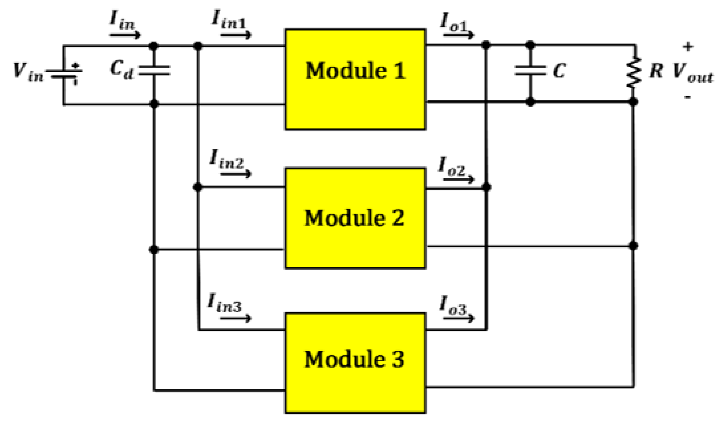
3. Input-Series Output-Parallel (ISOP) DC-DC Converter

All the related work in for the ISOP DC-DC converter, including system configuration, detailed SSM, and control strategy, has been previously published in [40].

4. Input-Parallel Output-Parallel (IPOP) DC-DC Converter

In this section, the IPOP DC-DC converter circuit diagram, as well as the IPOP DC-DC converter SSM, are discussed in detail.

4.1. IPOP Circuit Diagram

IPOP DC-DC converters are employed in high-current and high-power applications [44]. The IPOP converter configuration is shown in Figure 3, where the modules connected in parallel at the input and the output sides. This architecture is employed when the input side and the output side current are higher than the semiconductor devices’ current rating.
By ensuring equal Input Current Sharing (ICS) and Output Current Sharing (OCS), the input current per module is I i n 3 , and the output current per module is I o 3 . In which, I i n and I o , are the IPOP input current and the IPOP output current, respectively. The merits of the IPOP DC-DC converter can be highlighted in more accessible semiconductor devices selection due to the low current stress per module. Besides, a higher switching frequency can be achieved and accordingly lowering the size of the magnetic components.

4.2. IPOP Small-Signal Analysis

The SSM for the IPOP converter shown in Figure 4 is derived using the SSM presented in [37].
Since the input current per module is I i n 3 , and the output current per module is I o 3 , accordingly, the load resistance per module is 3 R . Therefore, d ^ i j , d ^ v j and I e q presented in Figure 4 can be expressed as follows, where the subscript   j = 1 , 2 ,   a n d   3 :
d ^ i j = 4   L l k f s K V i n i ^ L j
Rewriting (41) in terms of R d would result in:
d ^ i j = K R d V i n i ^ L j
d ^ v j = 4 L l k f s D e f f 3   k 2 R V i n v ^ i n
Similarly, rewriting (43) in terms of R d would result in:
d ^ v j = R d D e f f 3   R V i n v ^ i n
I e q = V i n 3 K R
The following equations are obtained from Figure 4:
{ D e f f K v ^ i n + V i n K ( d ^ i 1 + d ^ v 1 + d ^ 1 ) = s L i ^ L 1 + v ^ o u t D e f f K v ^ i n + V i n K ( d ^ i 2 + d ^ v 2 + d ^ 2 ) = s L i ^ L 2 + v ^ o u t D e f f K v ^ i n + V i n K ( d ^ i 3 + d ^ v 3 + d ^ 3 ) = s L i ^ L 3 + v ^ o u t
{ K 3 D e f f ( i ^ i n s C d v ^ i n ) = I e q ( d ^ i 1 + d ^ v 1 + d ^ 1 ) + i ^ L 1 K 3 D e f f ( i ^ i n s C d v ^ i n ) = I e q ( d ^ i 2 + d ^ v 2 + d ^ 2 ) + i ^ L 2 K 3 D e f f ( i ^ i n s C d v ^ i n ) = I e q ( d ^ i 3 + d ^ v 3 + d ^ 3 ) + i ^ L 3
j = 1 3 i ^ L j = v ^ o u t ( s C + 1 R )

4.2.1. Control-To-Output Voltage Transfer Function

The output voltage and the duty cycle relationship are found by summing up the KVL equations in (46), considering the same assumptions as in Section 2.2.1, and substituting (42), (44), and (48).
V i n K ( K R d V i n ( v ^ o u t ( s C + 1 R ) ) + j = 1 3 R d D e f f 3   R V i n v ^ i n + d ^ 1 ) = s L ( v ^ o u t ( s C + 1 R ) ) + 3 v ^ o u t
Simplifying (49) would result in (50):
G v d = v ^ o u t d ^ j = V i n K s 2 L C + s ( L R + R d C ) + R d R + 3

4.2.2. Control-To-Filter Inductor Current Transfer Function

The filter inductor current and the duty cycle relationship is found by substituting v ^ o u t in terms of i ^ L j using (48) in (49), and considering the same assumptions as in Section 2.2.1.
V i n K d ^ 1 R d j = 1 3 i ^ L j = s L j = 1 3 i ^ L j + 3 R s R C + 1 j = 1 3 i ^ L j
Simplifying (51) would result in (52):
G i d = i ^ L d ^ j = V i n K ( 1 + s R C ) R ( s 2 L C + s ( L R + R d C ) + R d R + 3 )

4.2.3. Control-To-Module Filter Inductor Current Transfer Function

The module filter inductor current and the duty cycle relationship is found by substituting (42), (44), and (48) in (46) assuming v ^ i n = 0 .
{ ( s L + R d + R s R C + 1 ) i ^ L 1 + R s R C + 1 i ^ L 2 + R s R C + 1 i ^ L 3 = V i n K d ^ 1 R s R C + 1 i ^ L 1 + ( s L + R d + R s R C + 1 ) i ^ L 2 + R s R C + 1 i ^ L 3 = V i n K d ^ 2 R s R C + 1 i ^ L 1 + R s R C + 1 i ^ L 2 + ( s L + R d + R s R C + 1 ) i ^ L 3 = V i n K d ^ 3
Subtracting the 2nd Equation in (53) from the 1st Equation in (53):
i ^ L 2 = i ^ L 1 V i n K ( s L + R d ) ( d ^ 1 d ^ 2 )
Similarly, subtracting the 3rd Equation in (53) from the 1st Equation in (53):
i ^ L 3 = i ^ L 1 V i n K ( s L + R d ) ( d ^ 1 d ^ 3 )
Substituting (54) and (55), in the first Equation in (53):
( s L + R d + 3 R s R C + 1 ) i ^ L 1 = V i n K [ ( 2 R ( s L + R d ) ( s R C + 1 ) + 1 ) d ^ 1 R ( s L + R d ) ( s R C + 1 ) d ^ 2 R ( s L + R d ) ( s R C + 1 ) d ^ 3 ]
Rearranging (56), the following equation is obtained:
i ^ L 1 = A ( s ) d ^ 1 + B ( s ) d ^ 2 + B ( s ) d ^ 3
where
A ( s ) = V i n ( s 2 L C R + s ( L + C R d R ) + R d + 2 R ) K ( s L + R d ) ( s 2 L C R + s ( L + C R d R ) + 3 R )
B ( s ) = V i n R K ( s L + R d ) ( s 2 L C R + s ( L + C R d R ) + 3 R )
Similar steps can be done for the filter inductor current for module 2 and module 3 such that:
{ i ^ L 1 = A ( s ) d ^ 1 + B ( s ) d ^ 2 + B ( s ) d ^ 3 i ^ L 2 = B ( s ) d ^ 1 + A ( s ) d ^ 2 + B ( s ) d ^ 3 i ^ L 3 = B ( s ) d ^ 1 + B ( s ) d ^ 2 + A ( s ) d ^ 3

4.2.4. Converter Output Impedance

Similarly, the IPOP converter output impedance can be found by modifying (48) such that:
j = 1 3 i ^ L j + i ^ o u t = v ^ o u t ( s R C + 1 R )
The output voltage and the output current relationship is found by considering the same assumptions as in Section 2.2.4, summing Equations in (46), and substituting (42), (44), and (61).
R d ( v ^ o u t ( s R C + 1 R ) i ^ o u t ) = s L ( v ^ o u t ( s R C + 1 R ) i ^ o u t ) + 3 v ^ o u t
Simplifying (62) would result in (63):
Z o u t = v ^ o u t i ^ o u t = ( R d + s L ) s 2 L C + s ( L R + R d C ) + R d R + 3

4.2.5. Converter Gain

The output voltage and the input voltage relationship is found by assuming d ^ j = 0 ,   j = 1 , 2 ,   and   3 , summing Equations in (46), and substituting (42), (44), and (48) in the added equation.
3 D e f f K ( 1 + R d 3 R ) v ^ i n = ( ( s L + R d ) ( s R C + 1 ) R + 3 ) v ^ o u t
Simplifying (64) would result in (65):
G v g = v ^ o u t v ^ i n = 3 D e f f K ( 1 + R d 3 R ) s 2 L C + s ( L R + R d C ) + R d R + 3

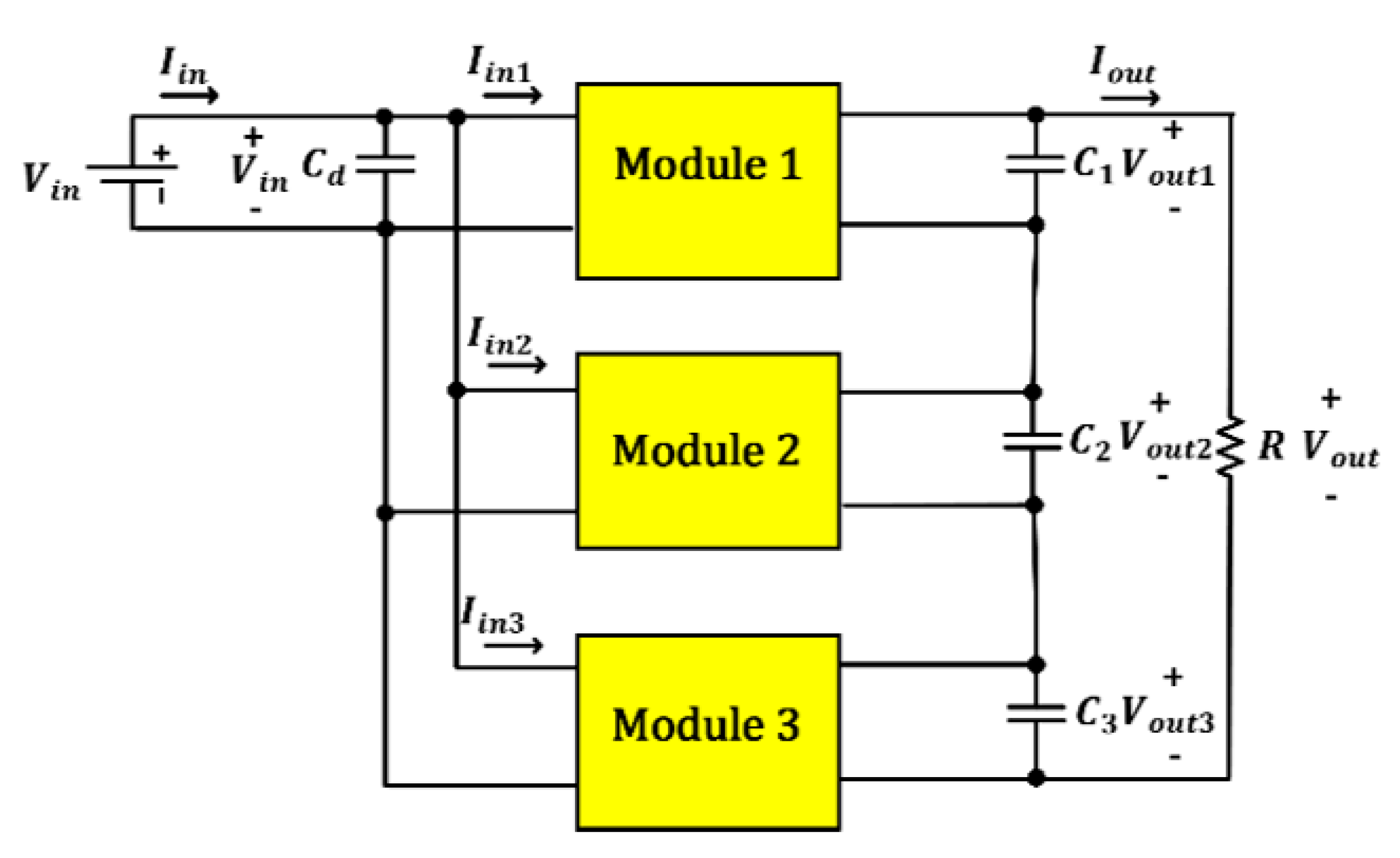
5. Input-Parallel Output-Series (IPOS) DC-DC Converter

In this section, the IPOS DC-DC converter circuit diagram, as well as the IPOS DC-DC converter SSM, are discussed in detail.

5.1. IPOS Circuit Diagram

IPOS DC-DC converters are employed in high input current and high output voltage applications [38]. The IPOS converter configuration is shown in Figure 5, where modules are connected in parallel and series at the input side and the output side, respectively. The IPOS DC-DC converter shown in Figure 5 is required for a high step-up ratio. This architecture is utilized when the output side current is within the semiconductor devices’ current rating.
By ensuring equal ICS and OVS, the input current per module is I i n 3 , and the output voltage per module is V o 3 . In which, I i n and V o , are the IPOS input current and the IPOS output voltage, respectively.

5.2. IPOS Small-Signal Analysis

The SSM for the IPOS converter shown in Figure 6 is derived using the SSM presented in [37].
Since the input current per module is I i n 3 , and the output voltage per module is V o 3 , accordingly, the load resistance per module is R 3 . Therefore, d ^ i j , d ^ v j and I e q presented in Figure 6 can be expressed as follows, where the subscript j = 1 , 2 ,   a n d   3 :
d ^ i j = 4   L l k f s K V i n i ^ L j
Rewriting (66) in terms of R d would result in:
d ^ i j = K R d V i n i ^ L j
d ^ v j = 12   L l k f s D e f f   k 2 R V i n v ^ i n
Similarly, rewriting (68) in terms of R d would result in:
d ^ v j = 3   R d D e f f   R V i n v ^ i n
I e q = 3   V i n K R
The following equations are obtained from Figure 6:
{ D e f f K v ^ i n + V i n K ( d ^ i 1 + d ^ v 1 + d ^ 1 ) = s L i ^ L 1 + v ^ o u t 1 D e f f K v ^ i n + V i n K ( d ^ i 2 + d ^ v 2 + d ^ 2 ) = s L i ^ L 2 + v ^ o u t 2 D e f f K v ^ i n + V i n K ( d ^ i 3 + d ^ v 3 + d ^ 3 ) = s L i ^ L 3 + v ^ o u t 3
{ K 3 D e f f ( i ^ i n s C d v ^ i n ) = I e q ( d ^ i 1 + d ^ v 1 + d ^ 1 ) + i ^ L 1 K 3 D e f f ( i ^ i n s C d v ^ i n ) = I e q ( d ^ i 2 + d ^ v 2 + d ^ 2 ) + i ^ L 2 K 3 D e f f ( i ^ i n s C d v ^ i n ) = I e q ( d ^ i 3 + d ^ v 3 + d ^ 3 ) + i ^ L 3
{ i ^ L 1 = s C v ^ o u t 1 + v ^ o u t R i ^ L 2 = s C v ^ o u t 2 + v ^ o u t R i ^ L 3 = s C v ^ o u t 3 + v ^ o u t R
Summing Equations in (73) would result in (74):
j = 1 3 i ^ L j = v ^ o u t ( s C + 3 R )
where
v ^ o u t 1 + v ^ o u t 2 + v ^ o u t 3 = v ^ o u t

5.2.1. Control-To-Output Voltage Transfer Function

The output voltage and the duty cycle relationship is found by summing up Equations in (71), considering the same assumptions as in Section 2.2.1, and substituting (67), (69), and (74).
3 D e f f K v ^ i n + V i n K ( K R d V i n ( v ^ o u t ( s C + 3 R ) ) + j = 1 3 3   R d D e f f   R V i n v ^ i n + d ^ 1 ) = s L ( v ^ o u t ( s C + 3 R ) ) + v ^ o u t
Simplifying (76) would result in (77):
G v d = v ^ o u t d ^ j = V i n K s 2 L C + s ( 3 L R + R d C ) + 3 R d R + 1

5.2.2. Control-To-Filter Inductor Current Transfer Function

The filter inductor current and the duty cycle relationship is found by substituting v ^ o u t in terms of i ^ L j using (74) in (76) and considering the same assumptions as in Section 2.2.1.
V i n K d ^ 1 R d j = 1 3 i ^ L j = s L j = 1 3 i ^ L j + R s R C + 3 j = 1 3 i ^ L j
Simplifying (78) would result in (79):
G i d = i ^ L d ^ j = V i n K ( 3 + s R C ) R ( s 2 L C + s ( 3 L R + R d C ) + 3 R d R + 1 )

5.2.3. Control-To-Module Filter Inductor Current Transfer Function

The filter inductor current and the duty cycle relationship is found by performing the following:
Substituting (75) in (76):
{ i ^ L 1 = ( s C + 1 R ) v ^ o u t 1   + 1 R v ^ o u t 2 + 1 R v ^ o u t 3 i ^ L 2 = 1 R v ^ o u t 1   + ( s C + 1 R ) v ^ o u t 2 + 1 R v ^ o u t 3 i ^ L 3 = 1 R v ^ o u t 1   + 1 R v ^ o u t 2 + ( s C + 1 R ) v ^ o u t 3
Rewriting (80) in terms of the output voltages:
{ v ^ o u t 1 = g 1 i ^ L 1 g 2 i ^ L 2 g 2 i ^ L 3 v ^ o u t 2 = g 2 i ^ L 1 g 1 i ^ L 2 g 2 i ^ L 3 v ^ o u t 3 = g 2 i ^ L 1 g 2 i ^ L 2 g 1 i ^ L 3
where
g 1 = 2 + s R C S 2 C 2 R + 3 s C       g 2 = 1 S 2 C 2 R + 3 s C
Rewriting (81) in a matrix form:
[ v ^ o u t 1 v ^ o u t 2 v ^ o u t 3 ] = [ g 1 g 2 g 2 g 2 g 1 g 2 g 2 g 2 g 1 ] [ i ^ L 1 i ^ L 2 i ^ L 3 ]
Substituting (67), (69), and (81) in (71) and assuming v ^ i n = 0 would result in:
{ V i n K d ^ 1 = ( s L + R d + g 1 ) i ^ L 1 g 2 i ^ L 2 g 2 i ^ L 3 V i n K d ^ 2 = g 2 i ^ L 1 + ( s L + R d + g 1 ) i ^ L 2 g 2 i ^ L 3 V i n K d ^ 3 = g 2 i ^ L 1 g 2 i ^ L 2 + ( s L + R d + g 1 ) i ^ L 3
Rearranging (84), the control-to-module filter inductor current can be represented as:
[ d ^ 1 d ^ 2 d ^ 3 ] = [ g 3 g 4 g 4 g 4 g 3 g 4 g 4 g 4 g 3 ] [ i ^ L 1 i ^ L 2 i ^ L 3 ]
where
S g 3 = V i n ( s L + R d + g 1 g 2 ) K ( g 1 2 g 1 g 2 + 2 g 1 g 5 2 g 2 2 g 2 g 5 + g 5 2 )
g 4 = V i n g 2 K ( g 1 2 g 1 g 2 + 2 g 1 g 5 2 g 2 2 g 2 g 5 + g 5 2 )
g 5 = s L + R d

5.2.4. Converter Output Impedance

Similarly, the IPOS converter output impedance can be found by modifying (74) such that:
j = 1 3 i ^ L j + i ^ o u t = v ^ o u t ( s C + 3 R )
The output voltage and the output current relationship is found by considering the same assumptions as in Section 2.2.4, summing Equations in (71), and substituting (67), (69), (75) and (89).
R d ( v ^ o u t ( s C + 3 R ) i ^ o u t ) = s L ( v ^ o u t ( s C + 3 R ) i ^ o u t ) + v ^ o u t
Simplifying (90) would result in (91):
Z o u t = v ^ o u t i ^ o u t = 3 ( R d + s L ) s 2 L C + s ( 3 L R + R d C ) + 3 R d R + 1

5.2.5. Converter Gain

The output voltage and the input voltage relationship is found by assuming d ^ j = 0 ,   j = 1 , 2 ,   and   3 , summing Equations in (71) and substituting (67), (69), and (74) in the added equation.
3 D e f f K ( 1 + 3 R d R ) v ^ i n = ( ( s L + R d ) ( s R C + 3 ) R + 1 ) v ^ o u t
Simplifying (92) would result in (93):
G v g = v ^ o u t v ^ i n = 3 D e f f K ( 1 + 3 R d R ) s 2 L C + s ( 3 L R + R d C ) + 3 R d R + 1

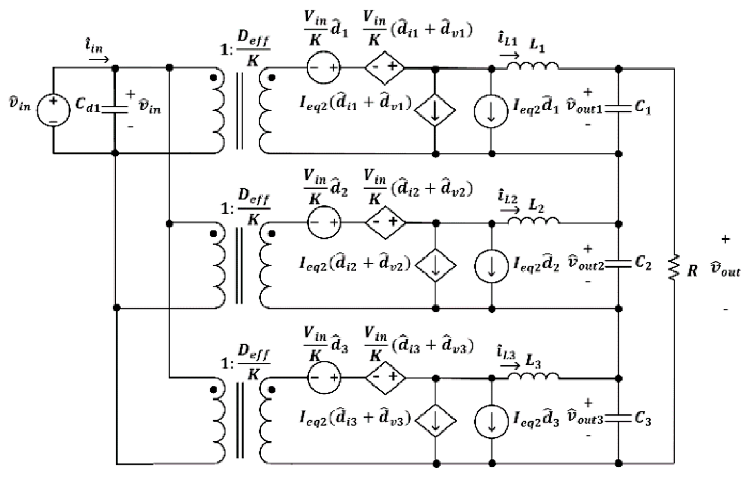
6. Generalized Small-Signal Analysis for Dual Series/Parallel Input-Output (ISIP-OSOP) DC-DC Converter

In this section, the SSM for the four architectures is expanded to include a generalized SSM applicable for ISIP-OSOP configuration. In addition, after generalizing the model, the equations derived in this section are validated with the IPOS, ISOP, and ISIPOS presented in [38,39,40,41,42], respectively.

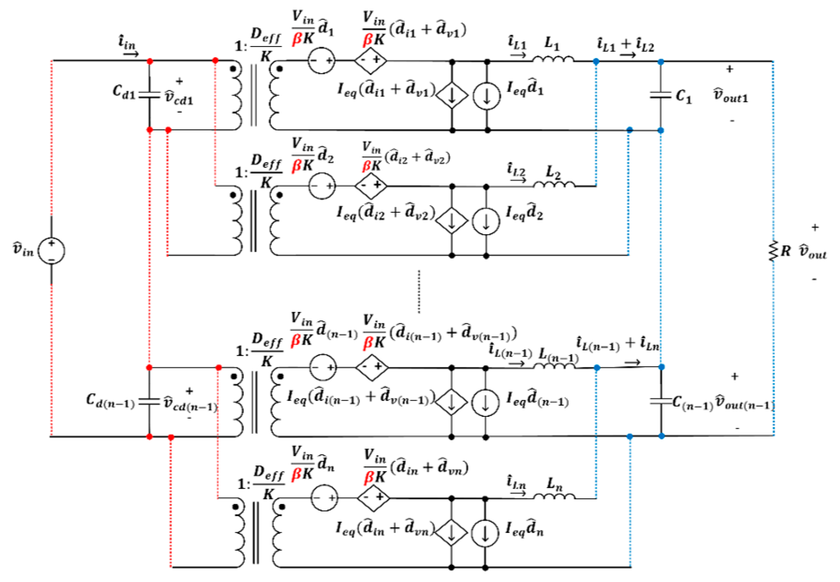
6.1. ISIP-OSOP Generic DC-DC Converter Circuit Diagram

The ISIP-OSOP generic DC-DC converter configuration shown in Figure 7 consists of n modules that are connected in series and/or parallel at the input side, and in series and/or parallel at the output side, as shown in Figure 7.
By ensuring ICS and IVS, the input current per module is I i n α , and the input voltage per module is V i n β . In which, I i n is the input current and V i n is the input voltage of the ISIP-OSOP DC-DC converter, and α is the number of modules connected in parallel, and β is the number of modules connected in series at the input side. Similarly, by ensuring OCS and OVS, the output current per module is I o a , and the output voltage per module is V o b . In which I o is the output current and V o is the output voltage of the ISIP-OSOP DC-DC converter, and a is the number of modules connected in parallel, and b is the number of modules connected in series at the output side.

6.2. ISIP-OSOP Generic DC-DC Converter Small-Signal Analysis

The SSM for the ISIP-OSOP converter shown in Figure 8 is derived using the SSM presented in [37], and expanding the study of the presented multimodule DC-DC converters presented in [38,39,40,41,42].
Since the input current and voltage per module are I i n α and V i n β , respectively, and the output current and voltage per module is I o a and V o b , respectively. Therefore, the load resistance per module is a b R . Accordingly, d ^ i j and d ^ v j , which are the effect of changing the filter inductor current and the effect of changing the input voltage on the duty cycle modulation, as well as I e q presented in Figure 8 can be expressed as [39,42]:
S d ^ i j = 4 β L l k f s K V i n i ^ L j ,         j = 1 , 2 , , n
Equation (94) can be re-written as:
d ^ i j = β K R d V i n i ^ L j ,         j = 1 , 2 , , n
where R d = 4 L l k f s k 2 .
d ^ v j = 4 β b L l k f s D e f f a k 2 R V i n v ^ c d j ,         j = 1 , 2 , , n
Equation (96) can be re-written as:
d ^ v j = β b R d D e f f a R V i n v ^ c d j ,         j = 1 , 2 , , n
S I e q = b V i n β a K R
The following equations are obtained from Figure 8:
{ D e f f K v ^ c d 1 + V i n β K ( d ^ i 1 + d ^ v 1 + d ^ 1 ) = s L i ^ L 1 + v ^ o u t 1 D e f f K v ^ c d 2 + V i n β K ( d ^ i 2 + d ^ v 2 + d ^ 2 ) = s L i ^ L 2 + v ^ o u t 2 D e f f K v ^ c d n + V i n β K ( d ^ i n + d ^ v n + d ^ n ) = s L i ^ L n + v ^ o u t n
{ i ^ L 11 + i ^ L 21 + + i ^ L a 1 = s C s R c C + 1 v ^ o u t 1   + v ^ o u t R i ^ L 12 + i ^ L 22 + + i ^ L a 2 = s C s R c C + 1 v ^ o u t 2   + v ^ o u t R i ^ L 1 b + i ^ L 2 b + + i ^ L a b = s C s R c C + 1 v ^ o u t n   + v ^ o u t R
Based on the feature of modularity, it is assumed that all the employed modules are ideal. Moreover, the Equivalent Series Resistance (ESR) of the output capacitance is considered in this model.
Summing Equations in (100):
i = 1 a j = 1 b i ^ L i j = s C s R c C + 1 v ^ o u t + b v ^ o u t R
Equation (101) can be written as:
i = 1 a j = 1 b i ^ L i j = v ^ o u t ( s R C + s b R c C + b R ( 1 + s R c C ) )
Defining the summation terms of the module’s input and output voltage appearing after summing up Equations in (99):
j = 1 n v ^ c d j = γ v ^ i n
where:
  • γ = 1 , if all the modules at the input side are connected in series.
  • γ = α , if all the modules at the input side are connected in parallel.
  • γ = ( 1 + α β ) , if the modules at the input side are connected in series and parallel.
j = 1 n v ^ o u t j = c v ^ o u t
where:
  • c = 1 , if all the modules at the output side are connected in series.
  • c = a , if all the modules at the output side are connected in parallel.
  • c = ( 1 + a b ) , if the modules at the output side are connected in series and parallel.

6.2.1. Control-To-Output Voltage Transfer Function

The output voltage and the duty cycle relationship is found by summing up Equations in (99), assuming v ^ i n = 0 , and d ^ k = 0 , where k = 1 ,   2 ,   ,   n and k j , and substituting (95), (97), (102), (103), and (104).
Summing Equations in (99):
D e f f K j = 1 n v ^ c d j + V i n β K ( j = 1 n d ^ i j + j = 1 n d ^ v j + j = 1 n d ^ j ) = s L j = 1 n i ^ L j + j = 1 n v ^ o u t j
D e f f K j = 1 n v ^ c d j + V i n β K ( j = 1 n β K R d V i n i ^ L j + j = 1 n β b R d D e f f a R V i n v ^ c d j + d ^ 1 ) = s L j = 1 n i ^ L j + j = 1 n v ^ o u t j
D e f f K γ v ^ i n + V i n β K ( j = 1 n β K R d V i n i ^ L j + β b R d D e f f a R V i n γ v ^ i n + d ^ 1 ) = s L j = 1 n i ^ L j + c v ^ o u t
Simplifying (107) would result in (108).
G v d = v ^ o u t d ^ j = V i n β K ( 1 + s R c C ) s 2 L C ( 1 + b R c R ) + s ( b L R + R d C ( 1 + b R c R ) + c R c C ) + b R d R + c

6.2.2. Control-To-Filter Inductor Current Transfer Function

The filter inductor current and the duty cycle relationship is found by using (102) to find the following equation:
v ^ o u t = R ( 1 + s R c C ) s R C + s b R c C + b i = 1 a j = 1 b i ^ L i j
Substituting (109) in (107) and considering the same assumptions as in Section 7.2.
V i n β K d ^ 1 R d j = 1 n i ^ L j = s L j = 1 n i ^ L j + c R ( 1 + s R c C ) s R C + s b R c C + b j = 1 n i ^ L j
Simplifying (110) would result in (111).
G i d = i ^ L d ^ = V i n β K ( b + s R C + s b R c C ) R ( s 2 L C ( 1 + b R c R ) + s ( b L R + R d C ( 1 + b R c R ) + c R c C ) + b R d R + c )

6.2.3. Output Impedance

Similarly, as studied in the SSM presented in [39,40], the ISIP-OSOP converter output impedance can be found by modifying (100), such that:
{ i ^ L 11 + i ^ L 21 + + i ^ L a 1 + i ^ o u t = s C s R c C + 1 v ^ o u t 1   + v ^ o u t R i ^ L 12 + i ^ L 22 + + i ^ L a 2 + i ^ o u t = s C s R c C + 1 v ^ o u t 2   + v ^ o u t R i ^ L 1 b + i ^ L 2 b + + i ^ L a b + i ^ o u t = s C s R c C + 1 v ^ o u t n   + v ^ o u t R
Summing Equations in (112):
i = 1 a j = 1 b i ^ L i j = s C s R c C + 1 v ^ o u t + b v ^ o u t R b i ^ o u t
Accordingly, (100) is modified as follows:
i = 1 a j = 1 b i ^ L i j = v ^ o u t ( s R C + s b R c C + b R ( 1 + s R c C ) ) b i ^ o u t
The output voltage and the output current relationship is found by considering the same assumptions as in Section 7.2, summing Equations in (99), and substituting (95), (97), (103), (104), and (114).
V i n β K ( β K R d V i n ) j = 1 n i ^ L j = s L j = 1 n i ^ L j + c v ^ o u t
R d ( v ^ o u t ( s R C + s b R c C + b R ( 1 + s R c C ) ) b i ^ o u t ) = s L ( v ^ o u t ( s R C + s b R c C + b R ( 1 + s R c C ) ) b i ^ o u t ) + c v ^ o u t
Rearranging (116) would result in (117).
Z o u t = v ^ o u t i ^ o u t = b ( R d + s L ) ( 1 + s R c C ) s 2 L C ( 1 + b R c R ) + s ( b L R + R d C ( 1 + b R c R ) + c R c C ) + b R d R + c

6.2.4. Converter Gain

The output voltage and the input voltage relationship is found by assuming d ^ j = 0   ,   j = 1 , 2 ,   ,   n , summing Equations in (99), and substituting (95), (97), (102)–(104) in the added equation.
D e f f K j = 1 n v ^ c d j + V i n β K ( j = 1 n β K R d V i n i ^ L j + j = 1 n β b R d D e f f a R V i n v ^ c d j ) = s L j = 1 n i ^ L j + j = 1 n v ^ o u t j
D e f f K γ ( 1 + b R d a R ) v ^ i n = ( s L + R d ) ( v ^ o u t ( s R C + s b R c C + b R ( 1 + s R c C ) ) ) + c v ^ o u t
Rearranging (119) would result in (120).
G v g = v ^ o u t v ^ i n = D e f f K γ ( 1 + b R d a R ) ( 1 + s R c C ) s 2 L C ( 1 + b R c R ) + s ( b L R + R d C ( 1 + b R c R ) + c R c C ) + b R d R + c

6.3. ISIP-OSOP DC-DC Converter SSM Verification

In this section, the generalized multimodule DC-DC converter SSM is verified using three different models presented in [38,39,40,41,42].

6.3.1. Generalized Model Verification with a Two-Module IPOS DC-DC Converter

The proposed configuration in [38] consists of two modules that are connected in parallel at the input side, and series, at the output side, where the modules are FB-PS-based DC-DC converters. In this model, the effect of the ESR R c is ignored, accordingly, when verifying the model presented in [34] with the generalized model, R c should be equated to zero.
By ensuring ICS and OVS, the input current per module is I i n 2 . However, the input voltage per module is V i n . Regarding the output side, the output voltage per module is V o 2 . However, the output current per module is I o . In which, V i n is the IPOS input voltage, I i n is the IPOS input current, V o is the IPOS output voltage, and I o is the IPOS output current. Accordingly, the values for the six parameters that are previously defined are known and shown in Table 2.
Substituting the six parameters with their values in Equations (109), (112), (117), and (120) and substituting the ESR R c with zero in the generalized transfer functions would result in the transfer functions presented in Table 3.
As can be seen from Table 3, the derived generalized model matches the model presented in [38], where the R d term in the above transfer functions is substituted with its equivalence 4   L l k   f s K 2 .

6.3.2. Generalized Model Verification with a Three-Module ISOP DC-DC Converter

In this Section, the generalized model is validated with the three-module ISOP power converter model-derived and presented in [39,40]. The three-module ISOP configuration consists of three modules that are connected in series at the input side, and parallel at the output side. In this model, the effect of the ESR R c is considered, accordingly, when verifying the model presented [39] with the generalized model, R c should not be ignored.
By ensuring IVS and OCS, the input voltage per module is V i n 3 . However, the input current per module is I i n . Regarding the output side, the output current per module is I o 3 . However, the output voltage per module is V o . Accordingly, the values for the six parameters that are previously defined are known and shown Table 4.
Substituting the six parameters with their values in Equations (109), (112), (117), and (120) would result in the transfer functions presented in Table 5.
As can be seen from Table 5, the derived generalized model matches the model presented in [39,40].

6.3.3. Generalized Model Verification with a Four-Module ISIPOS DC-DC Converter

In this section, the generalized model is validated with the four-module ISIPOS power converter model presented in [41,42].
The four-module ISIPOS configuration consists of four modules that are connected in series and parallel at the input side, and series at the output side. In this model, the effect of the ESR R c is ignored, accordingly, when verifying the model presented in [41] with the generalized model, R c should be equated to zero.
By ensuring IVS, ICS, and OVS, the input voltage per module is V i n 2 and the input current per module is I i n 2 . Regarding the output side, the output voltage per module is V o 4 . However, the output current per module is I o . Accordingly, the values for the six parameters that are previously defined are known and shown in Table 6.
Substituting the six parameters with their values in Equations (109), (112), (117), and (120) would result in the transfer functions presented in Table 7.
As can be seen from Table 7, the derived generalized model matches the model presented in [41,42].

7. Power Balancing in ISIP-OSOP DC-DC Converters

To guarantee stable operation in the presence of parameter variations, a control strategy that ensures power balancing is essential to provide equal power distribution among the modules. In this section, the control strategy for each multimodule configuration is studied to ensure IVS, ICS, OVS, and OCS if needed.
The possible control strategies for the four configurations have been discussed in [45]. According to the study presented in [45], for input parallel-connected systems, OCS and OVS controllers are required for IPOP and IPOS DC-DC converters, respectively. However, for input series-connected systems, IVS and OVS are required for ISOS DC-DC converters, and IVS and OCS are required for ISOP DC-DC converters. To further illustrate, active power sharing control for input parallel-connected systems is achieved by designing ICS controllers that achieve OCS and OVS for IPOP and IPOS systems or by designing OCS controllers for IPOP systems and designing OVS controllers for IPOS systems that also achieves ICS between the employed modules. However, for input-series connected systems, IVS controllers are necessary to achieve OVS and OCS for ISOS and ISOP DC-DC converters. However, in [46], Cross Feedback OCS (CFOCS) has been proposed for ISOP systems to achieve OCS without the need for IVS controllers, hence simplifying the overall control design. This control strategy has been tested for a three-module ISOP DC-DC converter considering RC in [40] to achieve IVS and OCS.
Since this paper mainly focuses on multimodule DC-DC converters designed for EV fast chargers, the control scheme designed for the four DC-DC converters is current-controlled considering an RC technique that is termed as burp charging or negative pulse charging. This charging technique is based on applying a short negative pulse or a short discharge pulse during the charging cycle. Such an algorithm offers significant advantages that can be highlighted in shortening the charging time and lowering the rise in temperature. Generally, the RC technique consists of three charging sequences, which are: a positive charging pulse, a rest period where no charging occurs, and a negative charging pulse or a discharge pulse [47]. Accordingly, the designed control schemes are based on controlling the filter inductor current of the DC-DC converters such that the output current profile is based on RC. Consequently, for IPOP and IPOS DC-DC converters, active power sharing is achieved through controlling the filter inductor currents, as shown in Figure 9a, that accordingly achieves equal output current distribution for IPOP systems and equal voltage distribution for IPOS systems. However, active power sharing in the ISOP DC-DC converter is achieved through the CFOCS presented in [40,46] and shown in Figure 9b, which eliminates the need for IVS controllers and control the output currents of the converters. The difference between Figure 9a and b is that, in Figure 9b, the current feedback for the individual module is the summation of the other two output currents and not its output current. Unlike the three systems ISOP, IPOP, and IPOS, active power sharing in the ISOS system is achieved through the use of both IVS and OVS controllers. In other words, the control scheme for the ISOS DC-DC converter combines the control scheme presented in Figure 9a with an IVS control, resulting in Figure 9c. To clarify, three IVS controllers are designed for each module to achieve equal input voltage distribution between the employed modules. In addition, the filter inductor currents are controlled using a reference current with an RC profile to achieve equal OVS between the modules of the ISOS converter. Therefore, it can be said that the control scheme presented in Figure 9a is applicable for the four architectures with slight differences presented in Figure 9b,c.

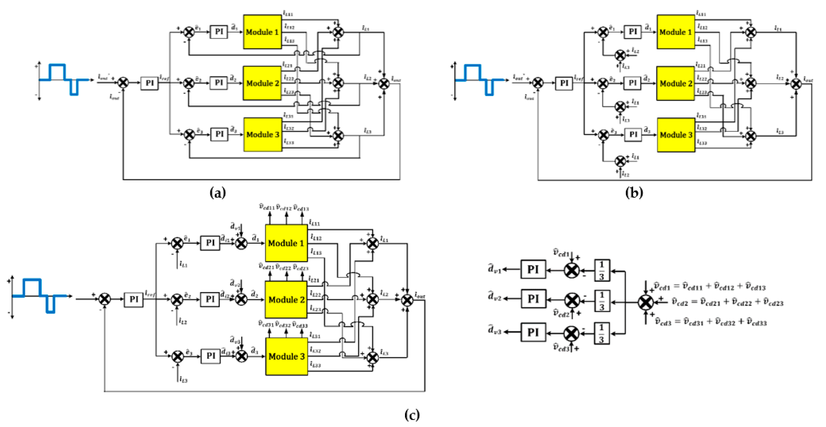
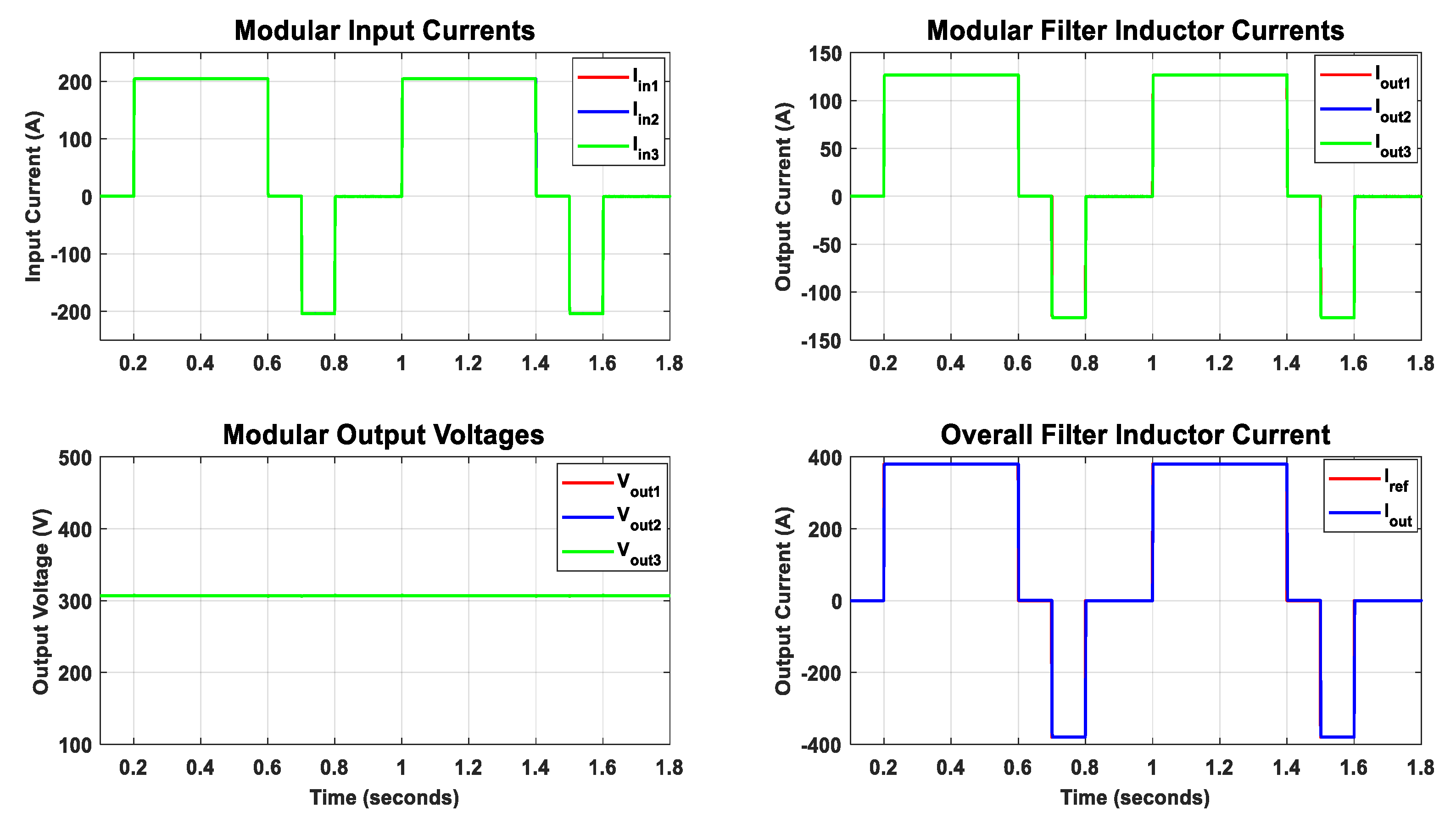
7.1. ISOS Control Strategy

In this Section, the ISOS DC-DC converter overall control scheme is examined with the system parameters presented in Table 8. To test the controller’s power balancing capability when handling uncertainties, the component parameters for each module are purposely assumed to be different, as presented in Table 8.
Talking about the simulation results, the control scheme presented in Figure 9c for the ISOS DC-DC converter is examined considering a reference current with a reflex-current profile to the total current flowing in the filter inductance. The charging pulse is applied, where the charging cycle begins at 0.2 s and ends at 0.6 s. After that, a rest period for 0.1 s is applied to the total filter inductor current reference signal. The results shown in Figure 10 demonstrate that the power-sharing controller presented in Figure 9c compensates for the negative influences resulting from the systems’ parameters mismatch. In which, the individual filter inductor currents are equally shared between the three modules. Moreover, the total filter inductor current of the ISOS system follows the reference signal applied based on RC. It is worth mentioning that the results in this section, as well as the following sections, involve the number of signals presented in the legend. However, the signals are coincident, meaning that power balance control is achieved. Consequently, it can be concluded that the control scheme is reliable and achieves equal power distribution between the modules.

7.2. ISOP Control Strategy

The overall control strategy for the ISOP system is examined and presented in [40] considering parameter mismatch for the three modules and a reference output current profile based on RC.

7.3. IPOP Control Strategy

In this Section, the IPOP DC-DC converter overall control scheme is examined with the system parameters presented in Table 9. To test the controller’s power balancing capability when handling uncertainties, the component parameters for each module are purposely assumed to be different, as presented in Table 9.
For parallel connected systems, active power-sharing control is achieved through directing the control efforts toward the output filter inductor currents without the need for any additional controllers. After designing the control scheme for the output filter inductor currents, the input currents are monitored to ensure that ICS is achieved through OCS. The same reference signal based on RC is applied to assess the controller scheme shown in Figure 9a. It can be observed from Figure 11 that the control scheme for the three-module IPOP system can achieve equal power distribution among the modules under parameter mismatch. In which, the modular input currents, as well as the modular output currents, are equally shared between the three modules. In addition, the overall filter inductor current of the IPOP power converter follows the reference signal applied based on RC.

7.4. IPOS Control Strategy

In this Section, the IPOS DC-DC converter overall control scheme is examined with the system parameters presented in Table 10. To test the controller’s power balancing capability when handling uncertainties, the component parameters for each module are purposely assumed to be different, as presented in Table 10.
In IPOS, OVS is achieved through controlling the filter inductor currents of each module. This accordingly achieves ICS between the three modules. The reference signal for the overall filter inductor current is also based on RC. It can be observed from Figure 12 that the control scheme for the three-module IPOS DC-DC converter presented in Figure 9a can achieve equal ICS and equal OVS among the employed IPOS modules. In which, the modular input currents, as well as the modular output voltages, are equally shared between the three modules. In addition, the overall filter inductor current follows the same current profile of the reference signal.

8. Conclusions

In recent years, EVs have gained attention because of their significant role in reducing CO2 emissions, minimizing noise pollution, avoiding the high price of fuel, and providing consumers with more efficient and environmentally friendly EVs. To allow for broader adoption of such EVs, diminishing the charging process would significantly increase the EV’s efficiency as well as their utilization. Towards this direction, advanced power electronics technologies are emerging significantly to achieve high efficiency as well as ensuring extended battery lifetime. Among these power electronics conversion systems, the DC-DC conversion stage plays a vital role in charging the EV’s battery. Consequently, this paper aims to present the four basic architectures for the modular DAB DC-DC converter with their SSM and control strategy to guarantee uniform power sharing among the modules. In addition, the main contribution of this paper can be summarized in providing generalized SSM for any multimodule connection, including ISIP-OSOP configurations to support in the design of the DC-DC stage control. In other words, the dynamic behavior of such multimodule converters is studied using the SSM to develop a generalized dual series/parallel input-output dual active bridge SSM applicable for EVs. The provided model is verified with three different models presented in the literature, which are: two-module IPOS converter, three-module ISOP converter, and four-module ISIPOS converter. Moreover, to assess the effectiveness of the control schemes, simulation results are presented where parameter mismatch is introduced between the modules to ensure power balancing in the overall converter system.

Author Contributions

For research articles with several authors, a short paragraph specifying their individual contributions must be provided. M.E. and A.M. contributed to the whole research work and analysis tools; M.E. wrote the paper. This work was performed under the supervision with regular and continuous feedback of A.M. All authors have read and agreed to the published version of the manuscript.

Funding

This work was supported by NPRP grant NPRP (10-0130-170286) from the Qatar National Research Fund (a member of Qatar Foundation).

Acknowledgments

This work was supported by NPRP grant NPRP (10-0130-170286) from the Qatar National Research Fund (a member of Qatar Foundation). The statements made herein are solely the responsibility of the authors.

Conflicts of Interest

The authors declare no conflict of interest.

Abbreviations

EVsElectric Vehicles
UFCUltra-Fast Charging
UF-EVCUltra-Fast EV Charging
SoCState-of-Charge
DABDual Active Bridge
DHBDual Half Bridge
ISOSInput-Series Output-Series
IPOPInput-Parallel Output-Parallel
ISOPInput-Series Output-Parallel
IPOSInput-Parallel Output-Series
SSMSmall-Signal Model
ISIP-OSOPInput-Series Input-Parallel Output-Series Output-Parallel
FB-PSFull-Bridge Phase-Shift
ISIPOSInput-Series Input-Parallel Output-Series
RCReflex Charging
IVSInput Voltage Sharing
OVSOutput Voltage Sharing
ICSInput Current Sharing
OCSOutput Current Sharing
ESREquivalent Series Resistance
CFOCSCross Feedback Output Current Sharing

References

  1. Vasiladiotis, M.; Rufer, A. A Modular Multiport Power Electronic Transformer with Integrated Split Battery Energy Storage for Versatile Ultrafast EV Charging Stations. IEEE Trans. Ind. Electron. 2015, 62, 3213–3222. [Google Scholar] [CrossRef]
  2. Kesler, M.; Kisacikoglu, M.C.; Tolbert, L.M. Vehicle-to-Grid Reactive Power Operation Using Plug-In Electric Vehicle Bidirectional Offboard Charger. IEEE Trans. Ind. Electron. 2014, 61, 6778–6784. [Google Scholar] [CrossRef]
  3. Hu, X.; Zou, C.; Tang, X.; Liu, T.; Hu, L. Cost-Optimal Energy Management of Hybrid Electric Vehicles Using Fuel Cell/Battery Health-Aware Predictive Control. IEEE Trans. Power Electron. 2020, 35, 382–392. [Google Scholar] [CrossRef] [Green Version]
  4. Teng, F.; Ding, Z.; Hu, Z.; Sarikprueck, P. Technical Review on Advanced Approaches for Electric Vehicle Charging Demand Management, Part I: Applications in Electric Power Market and Renewable Energy Integration. IEEE Trans. Ind. Appl. 2020. [Google Scholar] [CrossRef]
  5. Seth, A.K.; Singh, M. Resonant controller of single-stage off-board EV charger in G2V and V2G modes. IET Power Electron. 2020, 13, 1086–1092. [Google Scholar] [CrossRef]
  6. Zeb, M.Z.; Imran, K.; Khattak, A.; Janjua, A.K.; Pal, A.; Nadeem, M.; Zhang, J.; Khan, S. Optimal Placement of Electric Vehicle Charging Stations in the Active Distribution Network. IEEE Access 2020, 8, 68124–68134. [Google Scholar] [CrossRef]
  7. Christen, D.; Tschannen, S.; Biela, J. Highly efficient and compact DC-DC converter for ultra-fast charging of electric vehicles. In Proceedings of the 15th International Power Electronics and Motion Control Conference (EPE/PEMC), Novi Sad, Serbia, 2–4 September 2012; pp. LS5d.3-1–LS5d.3-8. [Google Scholar]
  8. Albert, G.B.; Andrew, C.C.; Suzanne, M.; David, L.W. Vehicle Electrification: Status and Issues. Proc. IEEE 2011, 99, 1116–1138. [Google Scholar]
  9. Pierre, M.; Jemelin, C.; Louvet, N. Driving an Electric Vehicle: A sociological analysis on pioneer users. Proc. Energy Effic. 2011, 4, 511–522. [Google Scholar] [CrossRef]
  10. Hidrue, M.; Parsons, G.; Kempton, W.; Gardner, M. Willingness to pay for electric vehicles and their attributes. Resour. Energy Econ. 2011, 33, 687–705. [Google Scholar] [CrossRef] [Green Version]
  11. Yilmaz, M.; Krein, P.T. Review of battery charger topologies, charging power levels and infrastructure for plug-in electric and hybrid vehicles. IEEE Trans. Power Electron. 2013, 28, 2151–2169. [Google Scholar] [CrossRef]
  12. Khaligh, A.; Dusmez, S. Comprehensive topological analysis of conductive and inductive charging solutions for plug-in electric vehicles. IEEE Trans. Veh. Technol. 2012, 61, 3475–3489. [Google Scholar] [CrossRef]
  13. Hartmann, M.; Friedli, T.; Kolar, J.W. Three-phase unity power factor mains interfaces of high power EV battery charging systems. In Proceedings of the Workshop ECPE Power Electronics for Charging Electric Vehicles, Valencia, Spain, 21–22 March 2011; pp. 1–66. [Google Scholar]
  14. Intel. Revolutionizing Fast Charging for Electric Vehicles; Intel: Santa Clara, CA, USA, 2013. [Google Scholar]
  15. Wang, S.; Crosier, R.; Chu, Y. Investigating the power architectures and circuit topologies for megawatt superfast electric vehicle charging stations with enhanced grid support functionality. In Proceedings of the 2012 IEEE International Electric Vehicle Conference, Greenville, SC, USA, 4–8 March 2012; pp. 1–8. [Google Scholar]
  16. Whitwam, R. BMW, Porsche Demo Super-Fast Electric Car Charger. ExtremeTech 2018. Available online: https://www.extremetech.com/extreme/282364-bmw-porsche-demo-super-fast-electric-car-charger (accessed on 9 March 2019).
  17. BMW. Ultra-Fast Charging Technology Ready for Future of Electric Vehicles. Electron. Compon. News 2018. Available online: https://www.ecnmag.com/news/2018/12/ultra-fast-charging-technology-ready-future-electric-vehicles (accessed on 9 March 2019).
  18. Yuan, Z.; Xu, H.; Chao, Y.; Zhang, Z. A novel fast charging system for electrical vehicles based on input-parallel output-parallel and output-series. In Proceedings of the 2017 IEEE Transportation Electrification Conference and Expo, Asia-Pacific (ITEC Asia-Pacific), Harbin, China, 2–5 August 2017; pp. 1–6. [Google Scholar]
  19. Beldjajev, V. Research and Development of the New Topologies for the Isolation Stage of the Power Electronic Transformer. Master’s Thesis, Tallinn University of Technology, Tallinn, Estonia, 2013. [Google Scholar]
  20. Engel, S.P.; Stieneker, M.; Soltau, N.; Rabiee, S.; Stagge, H.; de Doncker, R.W. Comparison of the Modular Multilevel DC Converter and the Dual-Active Bridge Converter for Power Conversion in HVDC and MVDC Grids. IEEE Trans. Power Electron. 2015, 30, 124–137. [Google Scholar] [CrossRef]
  21. Sari, H.I. DC/DC Converters for Multi-terminal HVDC Systems Based on Modular Multilevel Converter; Norwegian University of Science and Technology: Kongeriket, Norway, 2016. [Google Scholar]
  22. Yang, H. Modular and Scalable DC-DC Converters for Medium-/High-Power Applications. Master’s Thesis, Georgia Institute of Technology, Atlanta, GA, USA, 2017. [Google Scholar]
  23. Fan, H.; Li, H. A high-frequency medium-voltage DC-DC converter for future electric energy delivery and management systems. In Proceedings of the 8th International Conference on Power Electronics—ECCE Asia, Jeju, Korea, 30 May–1 June 2011; pp. 1031–1038. [Google Scholar]
  24. Papadakis, C. Protection of HVDC Grids Using DC Hub. Master’s Thesis, Delft University of Technology, Delft, The Netherlands, 2017. [Google Scholar]
  25. Carrizosa, M.J.; Benchaib, A.; Alou, P.; Damm, G. DC transformer for DC/DC connection in HVDC network. In Proceedings of the 15th European Conference on Power Electronics and Applications (EPE), Lille, France, 2–6 September 2013; pp. 1–10. [Google Scholar]
  26. Davidson, C.C.; Trainer, D.R. Innovative concepts for hybrid multi-level converters for HVDC power transmission. In Proceedings of the 9th IET International Conference on AC and DC Power Transmission (ACDC 2010), London, UK, 19–21 October 2010; pp. 1–5. [Google Scholar]
  27. Alatalo, M. Module Size Investigation on Fast Chargers for BEV; Chalmers University of Technology: Gothenburg, Sweden, 2018. [Google Scholar]
  28. Jalakas, T.; Roasto, I.; Vinnikov, D. Electric vehicle fast charger high voltage input multiport converter topology analysis. In Proceedings of the 2013 International Conference-Workshop Compatibility and Power Electronics, Ljubljana, Slovenia, 5–7 June 2013; pp. 326–331. [Google Scholar]
  29. Rivera, S.; Wu, B. Electric Vehicle Charging Station with an Energy Storage Stage for Split-DC Bus Voltage Balancing. IEEE Trans. Power Electron. 2017, 32, 2376–2386. [Google Scholar] [CrossRef]
  30. Rivera, S.; Wu, B.; Kouro, S.; Yaramasu, V.; Wang, J. Electric Vehicle Charging Station Using a Neutral Point Clamped Converter with Bipolar DC Bus. IEEE Trans. Ind. Electron. 2015, 62, 1999–2009. [Google Scholar] [CrossRef]
  31. Srdic, S.; Liang, X.; Zhang, C.; Yu, W.; Lukic, S. A SiC-based high-performance medium-voltage fast charger for plug-in electric vehicles. In Proceedings of the 2016 IEEE Energy Conversion Congress and Exposition (ECCE), Milwaukee, WI, USA, 18–22 September 2016; pp. 1–6. [Google Scholar]
  32. Aggeler, D.; Canales, F.; Zelaya, H.; La Parra, D.; Coccia, A.; Butcher, N.; Apeldoorn, O. Ultra-fast DC-charge infrastructures for EV-mobility and future smart grids. In Proceedings of the 2010 IEEE PES Innovative Smart Grid Technologies Conference Europe (ISGT Europe), Gothenburg, Sweden, 10–13 October 2010; pp. 1–8. [Google Scholar]
  33. Cui, T.; Liu, C.; Shan, R.; Wang, Y.; Kong, D.; Guo, J. A Novel Phase-Shift Full-Bridge Converter with Separated Resonant Networks for Electrical Vehicle Fast Chargers. In Proceedings of the 2018 IEEE International Power Electronics and Application Conference and Exposition (PEAC), Shenzhen, China, 4–7 November 2018; pp. 1–6. [Google Scholar]
  34. Justino, J.C.G.; Parreiras, T.M.; Filho, B.J.C. Hundreds kW Charging Stations for e-Buses Operating Under Regular Ultra-Fast Charging. IEEE Trans. Ind. Appl. 2016, 52, 1766–1774. [Google Scholar]
  35. Tian, Q.; Huang, A.Q.; Teng, H.; Lu, J.; Bai, K.H.; Brown, A.; McAmmond, M. A novel energy balanced variable frequency control for input-series-output-parallel modular EV fast charging stations. In Proceedings of the 2016 IEEE Energy Conversion Congress and Exposition (ECCE), Milwaukee, WI, USA, 18–22 September 2016; pp. 1–6. [Google Scholar]
  36. Vasiladiotis, M.; Rufer, A.; Béguin, A. Modular converter architecture for medium voltage ultra fast EV charging stations: Global system considerations. In Proceedings of the 2012 IEEE International Electric Vehicle Conference, Greenville, SC, USA, 4–8 March 2012; pp. 1–7. [Google Scholar]
  37. Vlatkovic, V.; Sabate, J.A.; Ridley, R.B.; Lee, F.C.; Cho, B.H. Small-signal analysis of the phase-shifted PWM converter. IEEE Trans. Power Electron. 1992, 7, 128–135. [Google Scholar] [CrossRef]
  38. Lian, Y.; Adam, G.; Holliday, D.; Finney, S. Modular input-parallel output-series DC/DC converter control with fault detection and redundancy. IET Gener. Transm. Distrib. 2016, 10, 1361–1369. [Google Scholar] [CrossRef] [Green Version]
  39. Ruan, X.; Chen, W.; Cheng, L.; Tse, C.K.; Yan, H.; Zhang, T. Control Strategy for Input-Series–Output-Parallel Converters. IEEE Trans. Ind. Electron. 2009, 56, 1174–1185. [Google Scholar] [CrossRef]
  40. ElMenshawy, M.; Massoud, A. Multimodule ISOP DC-DC Converters for Electric Vehicles Fast Chargers. In Proceedings of the 2nd International Conference on Smart Grid and Renewable Energy (SGRE), Doha, Qatar, 19–21 November 2019; pp. 1–6. [Google Scholar]
  41. Lian, Y.; Adam, G.P.; Holliday, D.; Finney, S.J. Medium-voltage DC/DC converter for offshore wind collection grid. IET Renew. Power Gener. 2016, 10, 651–660. [Google Scholar] [CrossRef]
  42. ElMenshawy, M.; Massoud, A. Multimodule DC-DC Converters for High-Voltage High-Power Renewable Energy Sources. In Proceedings of the 2nd International Conference on Smart Grid and Renewable Energy (SGRE), Doha, Qatar, 19–21 November 2019; pp. 1–6. [Google Scholar]
  43. Sha, D.; Guo, Z.; Luo, T.; Liao, X. A General Control Strategy for Input-Series–Output-Series Modular DC-DC Converters. IEEE Trans. Power Electron. 2014, 29, 3766–3775. [Google Scholar] [CrossRef]
  44. Cheng, J.; Shi, J.; He, X. A novel input-parallel output-parallel connected DC-DC converter modules with automatic sharing of currents. In Proceedings of the 7th International Power Electronics and Motion Control Conference, Harbin, China, 2–5 June 2012; pp. 1871–1876. [Google Scholar]
  45. Chen, W.; Ruan, X.; Yan, H.; Tse, C.K. DC/DC Conversion Systems Consisting of Multiple Converter Modules: Stability, Control, and Experimental Verifications. IEEE Trans. Power Electron. 2009, 24, 1463–1474. [Google Scholar] [CrossRef]
  46. Sha, D.; Guo, Z.; Liao, X. Cross-Feedback Output-Current-Sharing Control for Input-Series-Output-Parallel Modular DC–DC Converters. IEEE Trans. Power Electron. 2010, 25, 2762–2771. [Google Scholar] [CrossRef]
  47. Lee, C.S.; Lin, C.H.; Lai, S.-Y. Development of Fast Large Lead-Acid Battery Charging System Using Multi-state Strategy. Int. J. Comput. Consum. Control. (IJ3C) 2013, 2, 56–65. [Google Scholar]
Figure 1. Input-Series Output-Series (ISOS) DC-DC converter circuit diagram.
Energies 13 02540 g001
Figure 2. ISOS DC-DC converter small-signal modeling (SSM).
Energies 13 02540 g002
Figure 3. Input-Parallel Output-Parallel (IPOP) DC-DC converter circuit diagram.
Energies 13 02540 g003
Figure 4. IPOP DC-DC converter SSM.
Energies 13 02540 g004
Figure 5. Input-Parallel Output-Series (IPOS) DC-DC converter circuit diagram.
Energies 13 02540 g005
Figure 6. IPOS DC-DC converter SSM.
Energies 13 02540 g006
Figure 7. Generalized multimodule DC-DC converter circuit diagram.
Energies 13 02540 g007
Figure 8. n module Input-Series Input-Parallel Output-Series Output-Parallel (ISIP-OSOP) DC-DC converter SSM.
Energies 13 02540 g008
Figure 9. Control schemes for the four DC-DC converters; (a) control scheme used for input parallel-connected systems; (b) control scheme used for ISOP DC-DC converter; (c) control scheme used for ISOS DC-DC converter.
Energies 13 02540 g009
Figure 10. Simulation results for ISOS DC-DC converter: (a) modular filter inductor output currents and overall output current; (b) a zoomed-in illustration for the modular filter inductor output currents shown in (a).
Energies 13 02540 g010
Figure 11. Simulation results for IPOP DC-DC converter.
Energies 13 02540 g011
Figure 12. Simulation results for IPOS DC-DC converter.
Energies 13 02540 g012
Table 1. Electrical vehicle (EV) charging stations’ electrical specifications.
Charging LevelInput VoltagePhasePowerTime
Level 1 120   VAC (Single)
AC
1.5 2   kW 10 14 h
Level 2 208 / 240   VAC (Single)
AC
7 20   kW 1 3 h
Level 3 (DC Fast Charging) 480   VAC (Three)
DC
50 100   kW 12 24 min
Ultra-fast/Super-fast Charging 400   VAC
or
Medium Voltage ranging from
10 40   kV
(Three)
DC
300 700   kW < 3 min
Table 2. Values for the six parameters for a two-module Input-Parallel Output-Series (IPOS) power converter.
Defined Variables
Input Side α 2
β 1
γ 2 (same as α )
Output Side a 1
b 2
c 1
Table 3. Generalized model verification with the two-module IPOS power converter.
Transfer Functions for Two-Module IPOS DC-DC Converter
G v d V i n K s 2 L C + s ( 2 L R + R d C ) + 2 R d R + 1
G i d V i n K ( 2 + s R C ) R ( s 2 L C + s ( 2 L R + R d C ) + 2 R d R + 1 )
Z o u t 2 ( R d + s L ) s 2 L C + s ( 2 L R + R d C ) + 2 R d R + 1
G v g 2 D e f f K ( 1 + 2 R d R ) s 2 L C + s ( 2 L R + R d C ) + 2 R d R + 1
Table 4. Values for the six parameters for a three-module Input-Series Output-Parallel (ISOP) power converter.
Defined Variables
Input Side α 1
β 3
γ 1
Output Side a 3
b 1
c 3
Table 5. Generalized model verification with the three-module ISOP power converter.
Transfer Functions for Three-Module ISOP DC-DC Converter
G v d V i n 3 K ( 1 + s R c C ) s 2 L C ( 1 + R c R ) + s ( L R + R d C ( 1 + R c R ) + 3 R c C ) + R d R + 3
G i d V i n 3 K ( 1 + s R C + s R c C ) R ( s 2 L C ( 1 + R c R ) + s ( L R + R d C ( 1 + R c R ) + 3 R c C ) + R d R + 3 )
Z o u t ( R d + s L ) ( 1 + s R c C ) s 2 L C ( 1 + R c R ) + s ( L R + R d C ( 1 + R c R ) + 3 R c C ) + R d R + 3
G v g D e f f K ( 1 + R d 3 R ) ( 1 + s R c C ) s 2 L C ( 1 + R c R ) + s ( L R + R d C ( 1 + R c R ) + 3 R c C ) + R d R + 3
Table 6. Values for the six parameters for a four-module Input-Series Input-Parallel Output-Series (ISIPOS) power converter.
Defined Variables
Input Side α 2
β 2
γ 2 = ( 1 + α β )
Output Side a 1
b 4
c 1
Table 7. Generalized model verification with the four-module ISIPOS power converter.
Transfer Functions for Four-Module ISIPOS DC-DC Converter
G v d V i n 2 K s 2 L C + s ( 4 L R + R d C ) + 4 R d R + 1
G i d V i n 2 K ( 4 + s R C ) R ( s 2 L C + s ( 4 L R + R d C ) + 4 R d R + 1 )
Z o u t 4 ( R d + s L ) s 2 L C + s ( 4 L R + R d C ) + 4 R d R + 1
G v g 2 D e f f K ( 1 + 4 R d R ) s 2 L C + s ( 4 L R + R d C ) + 4 R d R + 1
Table 8. Input-Series Output-Series (ISOS) converter parameters.
ParametersFirst Module Second Module Third Module 3
Overall converter rated power 350   kW
Rated power per module 117   kW
Overall input voltage 10   kV
Input voltage per module 3.3   kV
Overall output voltage 920   V
Output voltage per module 307   V
Modules Number 3
Turns ratio 8.696 : 1 8.152 : 1 7.609 : 1
Leakage inductance 1142.72   μ H 1004.35   μ H 874.89   μ H
Effective duty cycle 0.8 0.75 0.7
Input Capacitance 50   μ F 80   μ F 60   μ F
Output filter inductor 50   mH 60   mH 60   mH
Output capacitance 300   μ F 350   μ F 300   μ F
Load resistance 2.418   Ω
Switching frequency 10   kHz
Table 9. Input-Parallel Output-Parallel (IPOP) converter parameters.
ParametersFirst Module Second Module Third Module 3
Overall converter rated power 350   kW
Rated power per module 117   kW
Overall input voltage   570   V
Input voltage per module 570   V
Overall output voltage 400   V
Output voltage per module 400   V
Modules Number 3
Turns ratio 1.14 : 1 1.069 : 1 1.003 : 1
Leakage inductance 3.712   μ H 3.262   μ H 2.871   μ H
Effective duty cycle 0.8 0.75 0.7
Input Capacitance 50   μ F 80   μ F 60   μ F
Output filter inductor 50   mH 60   mH 60   mH
Output capacitance 300   μ F 350   μ F 300   μ F
Load resistance 0.457   Ω
Switching frequency 10   kHz
Table 10. IPOS converter parameters.
ParametersFirst Module Second Module Third Module 3
Overall converter rated power 350   kW
Rated power per module 117   kW
Overall input voltage 570   V
Input voltage per module 570   V
Overall output voltage 920   V
Output voltage per module 307   V
Modules Number 3
Turns ratio 1.485 : 1 1.393 : 1 1.299 : 1
Leakage inductance 33.383   μ H 29.341   μ H 25.559   μ H
Effective duty cycle 0.8 0.75 0.7
Input Capacitance 50   μ F 80   μ F 60   μ F
Output filter inductor 50   mH 60   mH 60   mH
Output capacitance 300   μ F 350   μ F 300   μ F
Load resistance 2.421   Ω
Switching frequency 10   kHz

