1. Introduction
High voltage gas-insulated switchgear is compact metal enclosed switchgear, which offers outstanding reliability, operational safety, and environmental compatibility, and is used widely in electrical power transmission grid for tens of years. GIS commonly uses compressed sulfur hexafluoride (SF6) as dielectric gas. The performance of a GIS can be greatly degraded by presence of defects in the insulation system, such as conductive particles on the electrode or SF6–epoxy interface and voids in dielectric material, which may enhance the local electric field and cause localized discharge, and then cause breakdown of the gas gap or flashover of the gas-solid insulating material interface. In SF6 gas, under uniform field arrangements, the surface flashover voltage is considerably lower than the breakdown voltage of the gap without the spacer, and is further reduced in the presence of particle contamination. Metwally analyzed the main components and causes of the failures in GIS and showed that conductive particle accounted for the highest percentage of defects (~20%) [
1].
Many efforts have been made to clarify the influence on the withstand voltage, understand the flashover mechanism, and build a comprehensive model to describe the particle-initiated flashover. Conductive particles on the surface of the insulator can initiate partial discharge (PD) [
2], which can be a major source of the surface charge [
3] and cause a decrease of withstand AC voltage [
4,
5]. Cooke presented the significant influence of the particle on the flashover voltage of an insulator [
6], and experiments revealed that the flashover voltage of the conductive particle contaminated GIS insulator decreased monotonically with particle length and the application time of the voltage [
7,
8].
Due to the participation of the SF6–epoxy interface in the surface discharge process, the physical mechanism is more complex compared to pure SF6 gas, which is mature in discharge and breakdown theory. Cookson argued that secondary ionization processes from the insulator surface and trapped surface charges play a role [
9]. Cooke proposed a critical field model to predict the breakdown voltage of particle-contaminated system according to the streamer inception [
10]. Niemeyer derived an qualitative stepped-leader model for the discharge propagation along an insulator surface in compressed SF6 [
11]. Lim analyzed the influence of the distance between conductive particle and triple-junction on the flashover voltage of an epoxy surface and proposed a model to present the effect of positive space charge [
12]. Qi studied the PD feature of a conductive particle-contaminated GIS insulator under gradually-rising voltages and found different discharge modes under various voltages [
13]. Using a phase-space joint resolved method, Wu found that the conductive particle initiated PDs occur at different end of the particle in positive and negative half-cycle of the AC voltage and discharge mode changes from a corona-like discharge to a creepage-like discharge with increasing voltage [
14]. Sudarshan analyzed various models for different conditions and listed key processes in the flashover process for a comprehensive model [
15].
However, until now, the conductive particle-initiated flashover process has not been well defined, and our knowledge of flashover mechanisms of the contaminated GIS insulator does not seem to be complete [
4]. Although no comprehensive model of contaminated insulator surface flashover has been proposed, it can be accepted that the overall process is quite complex.
In this study, the PD process of a cone-type GIS insulator under constant high AC voltage up to flashover has been investigated, initiated by a conductive particle fixed on the concave surface. A data acquisition (DAQ) system for PD signal detection based on photomultiplier and high-speed analog-to-digital converter (ADC) has been built and PD signals up to the flashover have been captured through this DAQ system. The characteristics of the PD signals have been presented and analyzed, which may help to understand the process and discharge physics of the contaminated GIS insulator flashover under constant AC voltage.
2. Experiment System and Methods
2.1. Experiment System and PD Signal Detection
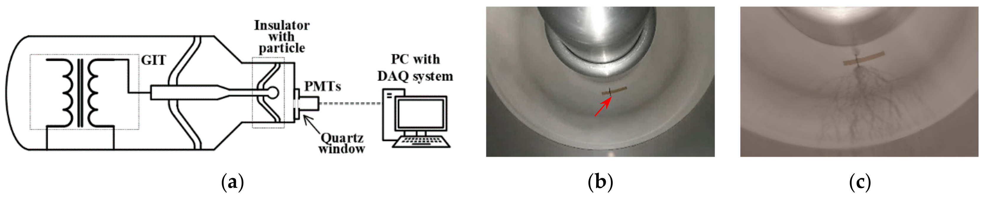
The experimental system is presented in
Figure 1a. A program-controlled gas insulated testing transformer (GIT) was used as the high voltage source, which can generate AC voltage up to 350 kV. A 100-kΩ protection resister was used to limit the short circuit current when flashover occurs. The flashover process of a 126-kV cone-type insulator has been studied using this test system under SF6 pressure of 0.4 MPa. The insulator was with an aluminum wire particle of 10-mm length and 0.7-mm diameter on its concave surface within the region with maximum electrical field strength, fixed by a narrow polyimide tape on the surface to avoid using glue which may influence the discharge process, as presented in
Figure 1b.
The particle can initiate PDs when the applied AC voltage goes higher than the PD inception voltage. The PD process generates a pulsed current signal, electromagnetic radiation, and light emission, which can be used for PD detection. In this paper, PMT is used to convert the weak light emissions from the PD process. The PMT used to detect PD signal is Hamamatsu CR131, which is sensitive to light with wavelengths of 185 nm to 900 nm and with very fast rising time of 2.2 ns. The performance of the PMT under a working voltage of ~1050 V is calibrated and the sensitivity is about 0.5 pC/mV at low signal amplitude. The calibration has been conducted by comparing the signal amplitudes of same PD event from the PMT and a calibrated PD checking circuit according to International Electrotechnical Commission (IEC) standard 60270-2015, under applied AC voltage 10 kV higher than the inception voltage of the partial discharge.
An industrial computer with the DAQ board was used to record the signal from PMT, as presented in
Figure 1a. One of the disadvantages of PMT is the dark count, that is, even without any light input, the PMT can generate output pulse signals occasionally. Due to the randomness of the dark count, it was difficult to distinguish it from the real PD signals. In this paper, an additional reference PMT was used to solve this problem. Because the possibility that the two PMTs generate dark count at the same time is extremely small, the signal from only one of the PMTs can be treated as fake signal and the signal from both of the PMTs at the same time can be recognized as the real PD signal.
The PMTs and a quartz-glass window were mounted on a base fixed at the end of the test chamber, which was made of opaque and insulated material to isolate the ambient light, reduce interference from transient ground level changing, and protect the DAQ system against the damage from large ground level change when flashover takes place. The signal output and the power supply cables of the PMTs were shielded to reduce the electromagnetic interference noise.
2.2. DAQ System and Data Collection Method
PD signals are widely used in defect detection and on-site monitoring of GIS [
16,
17,
18,
19]. The primary purpose of the PD detection system in this paper was to capture the waveform of each PD signal with high temporal resolution and high sensitivity throughout the test to find out detailed information about the PD process. The PD pulses captured by the PMTs were characterized by pulse width, rising and falling times of several nanoseconds, and needed DAQ system with a GHz sample rate. Long time testing with GHz sample rate will generate massive amounts of data, which is far beyond the processing capability of the DAQ system. Due to the sparse nature of the PD signal over time, a special DAQ mode was used accordingly to reduce the data transfer and storage.
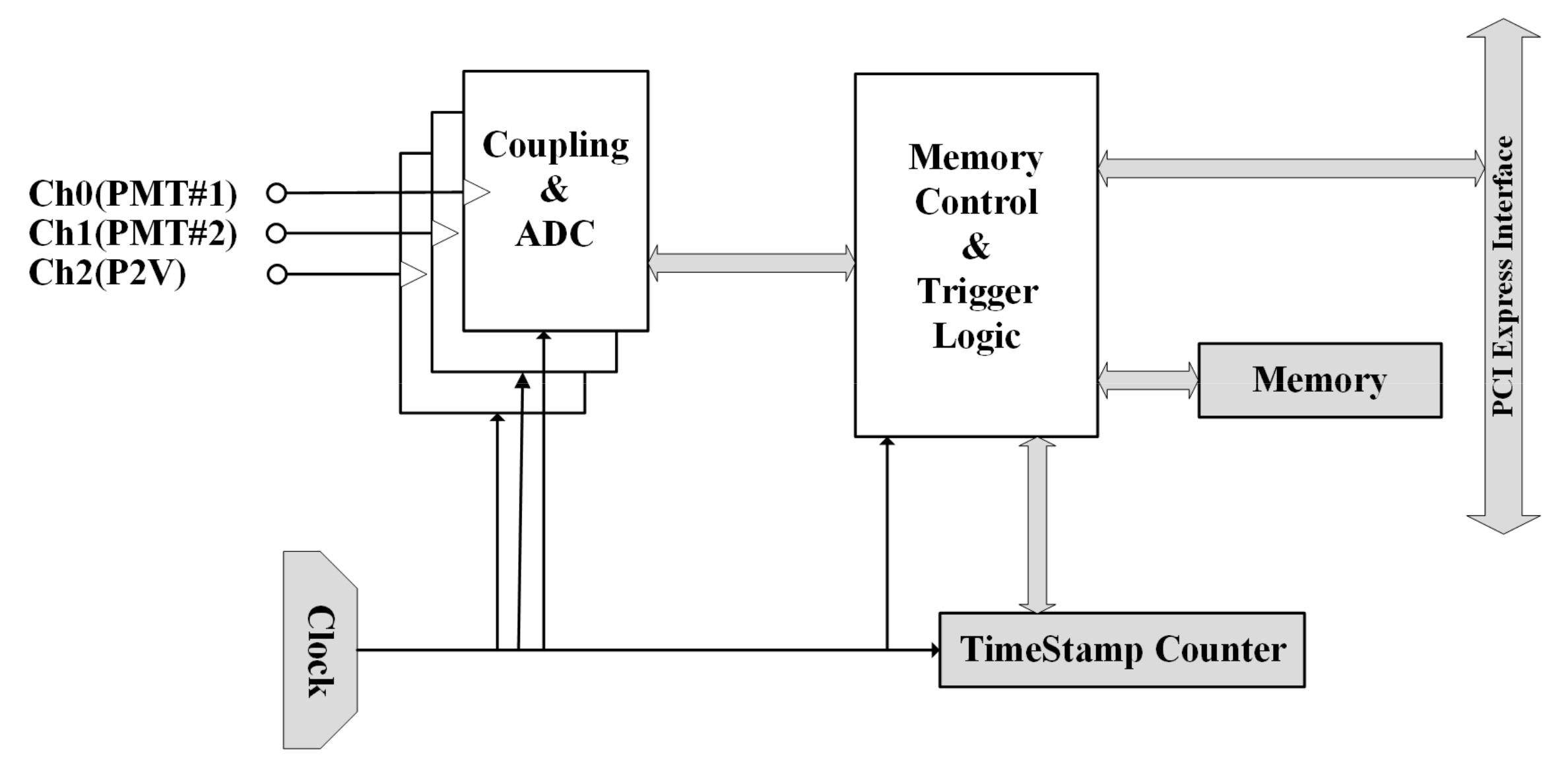
The block diagram of the data acquisition (DAQ) system is presented in
Figure 2. The DAQ system mainly consists of an analog-to-digital converter (ADC) circuit, memory control and trigger logic, buffer memory, internal clock, and a timestamp counter.
Two ADCs were used to convert the analog output of the PMTs to digital data, with 50 Ω input impedance, 500 MHz analog bandwidth and sample rate of 1.25 GSample/s. The onboard buffer memory was 4 GB, shared by all of the ADC channels.
The trigger logic started the transfer of data and timestamp to buffer memory and rearm the trigger for next event and the memory control manage the transfer of data and timestamp from ADC and timestamp counter to the buffer memory, and subsequently from the buffer memory to computer memory through the Peripheral Component Interconnect (PCI) Express bus. The data is stored in the buffer memory as a first-in, first-out (FIFO) queue, which can be written and read independently so as to make the ADC and the data transfer from the DAQ board to the computer can run independently until the buffer memory filled. This asynchronous mode of the DAQ system means the onboard PD signal acquisition can run at the peak rate, while the data transfer to computer can keep to a moderate rate, depending on the data amount in the onboard buffer memory.
The timestamp counter was a very wide counter running with the sampling clock. The counter can record the time of each trigger event relative to the start of the DAQ running through the system clock count. The timestamp counter is a 64-bit counter, which means the maximum time of the timestamp can be 264 system clock cycles.
The output of the PMT was a negative pulse, so the DAQ system worked on a negative edge trigger mode. The DAQ was triggered using ‘AND’ logical operation of trigger signals from each the PMT signal (Ch0 and CH1), while the trigger levels were set to −1.6 mV, slightly exceeding the background noise level. Random noise and dark signal of the PMT can be refused by the DAQ system using the ‘AND’ logic of the trigger event.
Because pulse width of the PMT signal of most PDs is only several nanoseconds, the DAQ system collects only a short segment data from the ADCs when trigger events occur to reduce the amount of data. Each segment contained 256 samples (64 samples before and 192 samples after the trigger event) which can cover the whole duration of the PD signal so as to record the waveform of each PD and obtain detailed PD information. The ADC data of each channel and the timestamp of the trigger event were then transferred to the buffer memory. This data acquisition mode greatly reduced the amount of data acquired and transferred to buffer memory and the computer storage memory, there was no data acquisition and transmission most of the time because of the sparse nature of the PD signal over time.
A phase-to-voltage (P2V) circuit was used to convert the phase to a sawtooth waveform with the same period of the AC voltage. The P2V signal was collected synchronously for each PD event (through CH2 of the DAQ system) and used to obtain the PRPD pattern of the PDs.
3. Results and Discussion
During the experiment, the applied high AC voltage increased to 90 kV from zero with rate of ~1kV/s, and then increased 5 kV with the same rate each 5 min until the voltage reached 140 kV. After that, the applied voltage was kept constant until the flashover occurred. The flashover took place nearly 9 h after the application of the high AC voltage in this test.
There were nearly 1.4 × 10⁶ PD pulses captured throughout the experiment. Due to the independent work mode of the ADCs and the data transfer process, the minimum lag of the trigger re-arm can be as low as one clock period after the previous data segment ADC finished. This feature ensures that there is very little chance to miss the PD signal due to the dead time of the DAQ system.
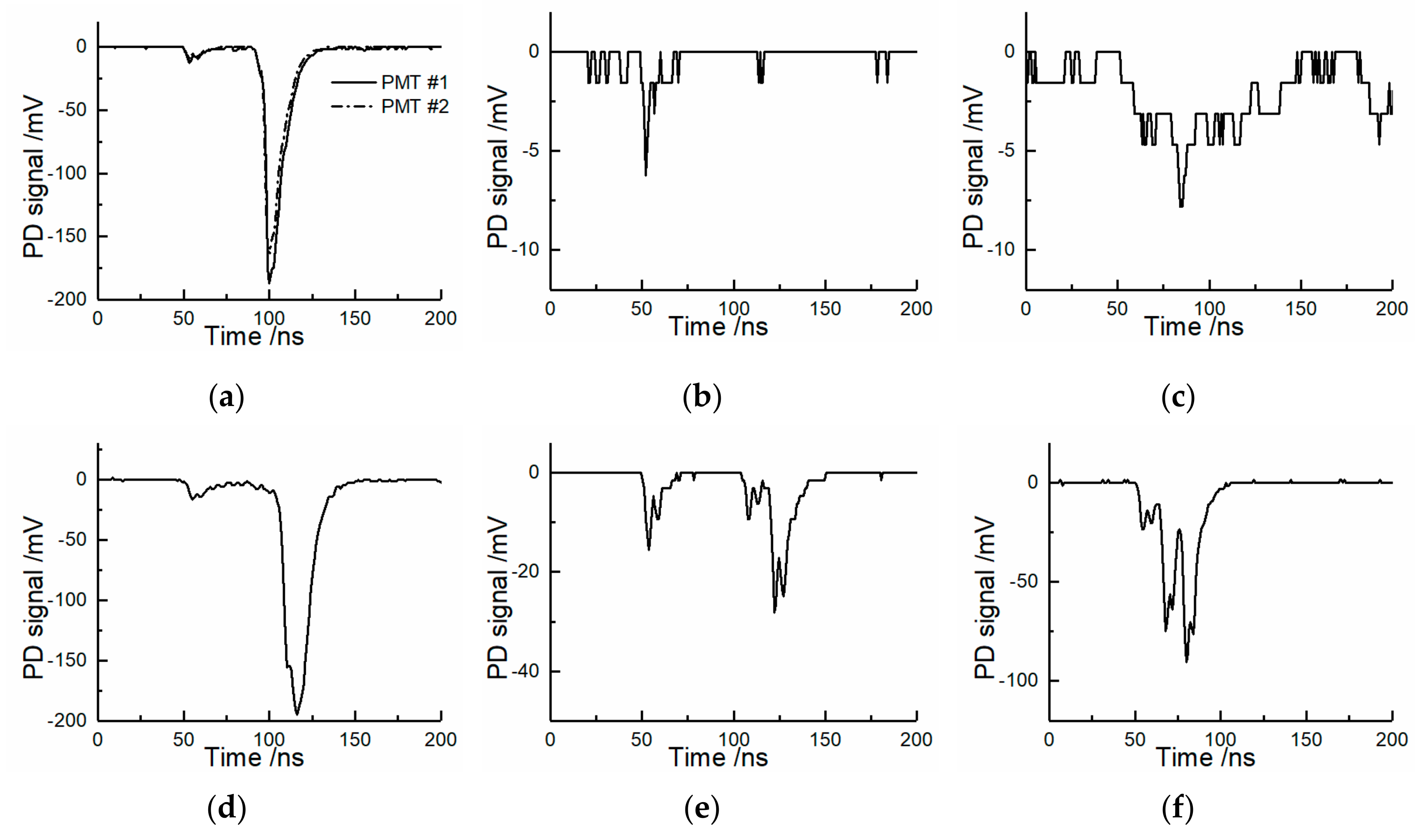
The intensity of the PD emitted light changes under different discharge conditions, and there were various types of signals from the PMTs corresponding to different PD processes. The typical PMT signals of the PD process are presented in
Figure 3. Due to the sensitivities and orientations of the two PMTs, the signal waveforms of the same PD were almost the same except a slight difference in amplitude, as presented in
Figure 3a.
The peak of each pulse was taken as the amplitude of each PD signal while the full width at half maximum (FWHM) of the pulse was taken as the pulse width. There were some signals with low amplitude and low pulse width, as presented in
Figure 3b, and signals with low amplitude and larger pulse width also existed, generated occasionally with very small count number during the test, as presented in
Figure 3c. This does not mean that there was weak PD process with relative longer duration. According to the waveform, it could most likely be a PD process consisting of multiple weak discharge processes. There were also some signals are with high amplitude and larger pulse width, as presented in
Figure 3d. Multiple PDs occurring in a very short time could generate signals like
Figure 3e, which consists of separated PD pulses, and
Figure 3f, which consists of overlapped PD pulses.
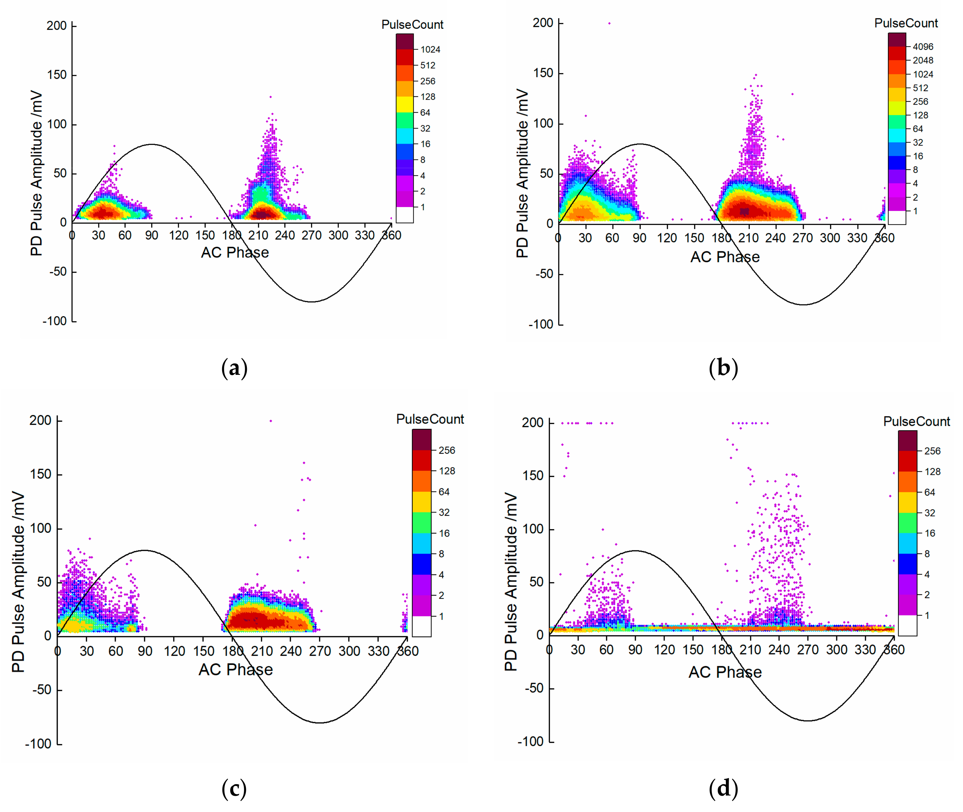
According to the PRPD patterns and the PD counts presented in the following text, the development of the discharge could be roughly divided into four stages, from the application of the high AC voltage up to the flashover of the insulator, which were: stage 1, from the application to 280 min; stage 2, from 280 min to 5 min before the flashover; stage 4, the last 2 s before the flashover; and stage 3, the last 5 min before stage 4. The spectra of amplitude over pulse width of the PD signals, PD counts, and PRPD patterns in these stages are presented as following.
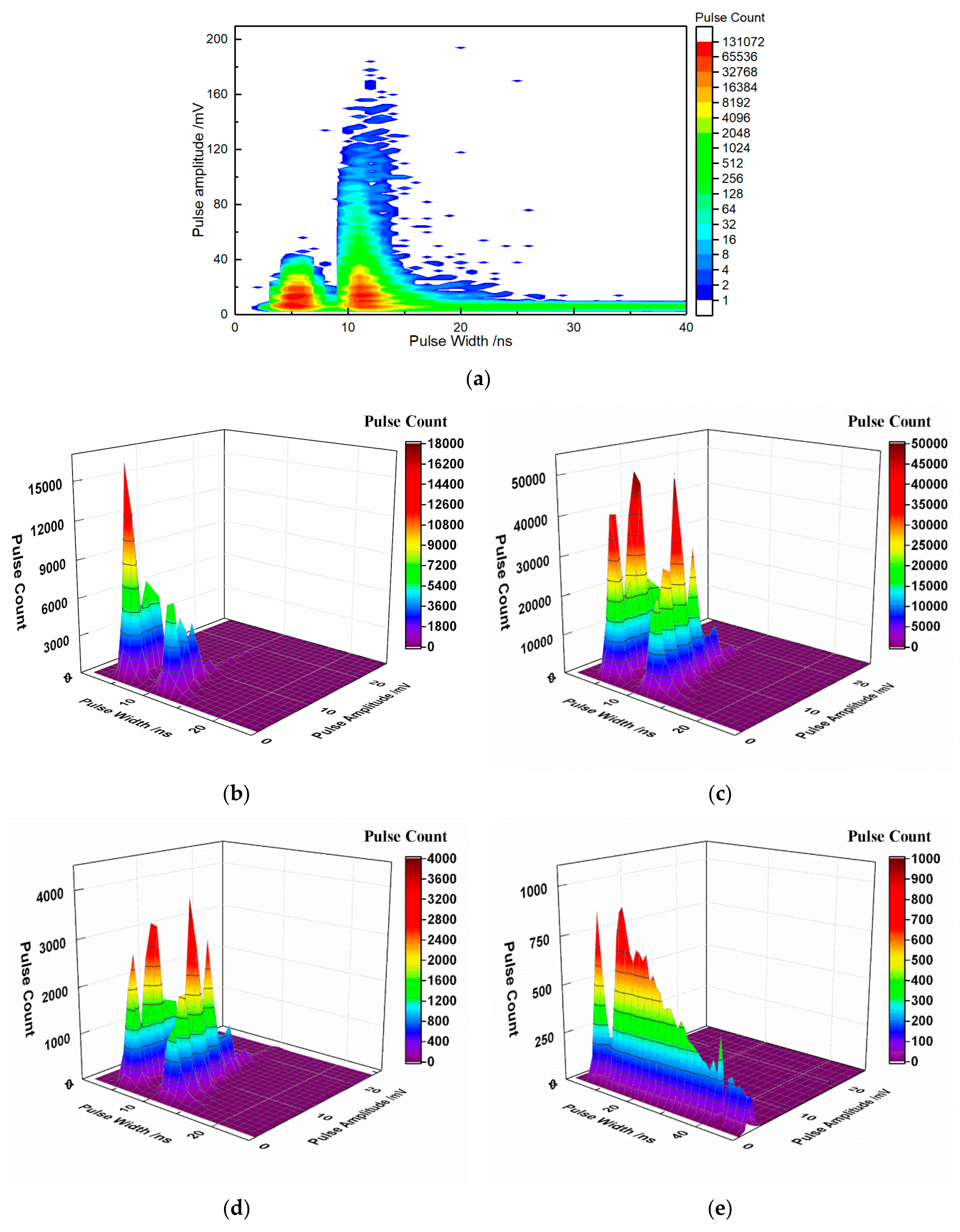
The amplitude and pulse width changed under different PD conditions. The spectra of pulse amplitude over the pulse width of the PMT signals are presented in
Figure 4. According to
Figure 4a, the PD signal can be divided to two main groups, group one with a smaller pulse width of ~5 ns and a second group with a larger pulse width of ~11 ns. The PD pulse in group one had an amplitude of less than 40 mV, and most of the amplitude was less than 20 mV. Similarly, most of the PD pulse in group two also had an amplitude of less than 20 mV. The PD pulse with a relatively lowerr count in group two was with an amplitude within 40 to 120 mV, and the PD pulse within 120 to 200 mV in group two was sporadic in the diagram. Although the amplitude of some rare PD pulses with large discharge values may exceed the input range of the ADCs, the input level of the ADCs was limited to −200 mV to ensure better resolution of most PD signals with low amplitude.
The apparent charge of the main part of the PD can be estimated to be less than 10 pC according to the calibrated sensitivity. Unfortunately, the apparent charge of the PD with high amplitude cannot be estimated credibly using this method because the intensity of the PD-emitted light increases non-linearly with the discharge value, especially for PDs with very large values.
PDs in group one had one peak, similar to the waveform presented in
Figure 3b, which corresponds to one discharge process occurring at the end of the particle with highest electrical field strength (called single-end discharge). The waveforms of most pulses in group two are with two consecutive peaks which always have similar pulse width and peak separation in time (called double-end discharge), similar to the waveform of an individual pulse in
Figure 3e,f, while this unique feature of these waveforms implies that two discharge processes exist in each individual pulse corresponding to the two peaks. It is most likely that the first discharge at one end of the particle triggers the following discharge at another end, due to the enhancement of the electrical field strength around the second end after discharge process at the first end.
In stage 1, the PDs with maximum count had a pulse width of ~5 ns and amplitude of 3~4 mV, which means that in stage 1 most of the particle-initiated PDs were single-end discharge. The lower count peak with the same pulse amplitude and larger width in
Figure 4b indicates that in this stage the double-end discharge occurred much less than the single-end discharge. There also existed other lower peaks and the multi-peak feature of the spectrum implied that there must be some specific discharge with similar processes. Peaks with similar pulse amplitude and two different pulse widths indicated that the single-end discharge may trigger the double-end discharge or not, depending on the conditions in which each discharge occurs.
In stage 2, spectrum peaked with higher amplitude emerged, while the pulse counts of peaks with larger pulse width also increased relatively, which means relatively more discharges with higher charge value occurred and more double-end discharges took place in stage 2.
In stage 3, the spectrum was similar to that in stage 2. But in stage 4, the last 2 s before flashover of the insulator, the spectrum showed completely different features; most the PD pulses had very low amplitude of ~3–4 mV and the pulse width was distributed in a wide range, as presented in
Figure 4e. The pulse widths may exceed 100 ns, and some of them approached 160 ns. Because the data segment for each pulse covered only 204.8 ns, it cannot be precluded that there were pulses with durations over 200 ns. The wide range of pulse widths comes from the overlap of a large number of PD pulses with very low amplitude, similar to the waveform presented in
Figure 3c, which means that, prior to the flashover, a large number of small discharges occurred successively in a very short time. Most of individual pulses corresponded to a corona-like discharge process, due to the low discharge value and the short duration. The sporadic PDs with both high amplitude and large pulse width imply the rare streamer-like or leader-like discharge process.
The PD features changed with time, which indicates the PDs develop the process and the conditions of the insulation system.
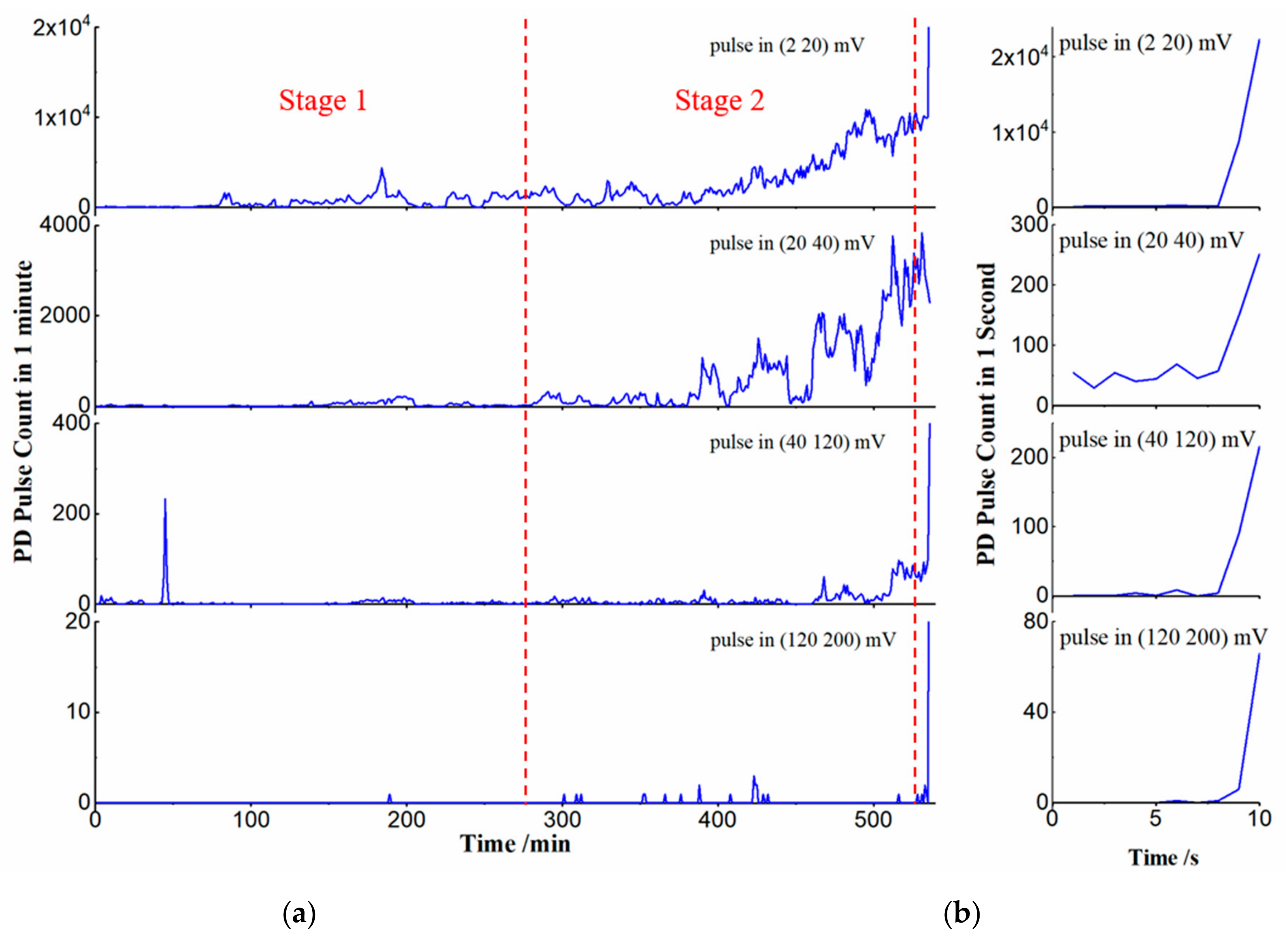
Figure 5a shows the variation of pulse counts in a 1 min period over time within various amplitude ranges. As presented in
Figure 5a, the PDs with amplitude in (2–20) mV were the main part of the PDs, and the PDs showed an intermittent count in stages 1 and 2. The PD count decreased sharply in 1~2 min when intermission came, and this intermittent feature also existed in the PD count in (20–40) mV. The intermittent feature may be caused by the space charge or the surface charge generated in the PDs. Although the surface charge is difficult to diffuse, the charged particles in the SF6 gas, such as free electrons, and negative and positive ions, can drift driven by the electrical field or diffuse due to the density gradient, while the space charge can also be trapped by the surface of the insulator, influencing the accumulation and density of the local surface charge. The space charge and surface charge may modify the local electrical field strength and enhance or weaken the local discharge process, depending on the specific condition.
The PD count rates in all of the amplitude ranges were very small in the early stages of the experiment, except the occasional high-count rate of pulse in (40–120) mV in the first half hour. The pulse count rate in (2–40) mV started to increase 1~2 h after the application of the high AC voltage. These PD count rates showed continuous increase after 6 h, while the intermittency still existed. The duration of the intermittent feature did not show any obvious regularity. PD signal with an amplitude higher than 40 mV was scarce during most of the experiment, especially when the amplitude was higher than 120 mV, as presented in
Figure 5a. The PD counts in a 1 s period in all of the amplitude ranges increased sharply 1~2 s before the flashover occurred, as presented in
Figure 5b, which implies that in the last 1~2 s the conditions of the insulated system changed dramatically.
Due to the much shorter duration of stage 4, the PD counts in
Figure 4e were much lower than those in
Figure 4b,c, but the count rate in the last stage was much higher, as presented in
Figure 5.
PRPD pattern is a commonly used method to analyze PD signals and can provide rich physical information on the PD process. PRPD patterns in different stages are presented in
Figure 6. In stages 1–3, the PDs took place in the first quarter of the positive and negative half-cycle of AC voltage and concentrated on specific phase in stage 1. PDs took place more frequently in the negative half-cycle, and PDs with high amplitude were also more frequent in this half-cycle in stages 1–3. As the discharge developed, PDs took place in a wider phase range in stages 2 and 3, while more PDs with high amplitude moved from the middle part of the first quarter of the negative half-cycle in stage 1–2 nearly to the negative peak in stage 3, as the purple dot with amplitude higher than 100 mV shows in
Figure 6a–c.
In the last stage, PDs took place on every phase, while the PDs with high amplitude still concentrated in the first quarter of the positive and negative half-cycle. Some pulses of PDs with extremely large discharge values even exceeded the input range of the ADCs, recorded by the DAQ system with an amplitude equal to 200 mV, as presented in
Figure 6d. PDs with amplitudes of 3–4 mV emerged in the second quarter of the positive and negative half-cycle for the first time. In stages 1–3, during the second quarter of the positive and negative half-cycle, the decreasing voltage may have weakened the local electrical field strength near the particle and then prevented PDs in this period. In stage 4, it is most likely that the accumulated space charge or surface charge exceeded a certain level and caused the local electrical field strength to be high enough to maintain dense low amplitude PDs even in the descending period of the AC voltage waveform. The dense small PDs then lead the discharge process like streamer-like or leader-like discharge with very large discharge value and finally induced the flashover of the insulator. Yoshida studied the intensities and spectra of the light emission from PDs of a needle-plane gap in SF6 under action of impulse voltage and found that the light intensity of the leader tip is much higher than that of the streamer [
20]. This phenomenon may verify the transition to the leader-like discharge according to the PD signals with very large amplitude in the final stage in this test.
Although the count and amplitude of the PD pulses were higher in the negative half-cycle of AC voltage, the flashover finally took place near the positive peak of AC voltage in the final stage. Tests with different particle length have also been conducted under the same conditions, and PD features in these tests were similar, but the time lags to flashover were different.


