Article

Analysis and Implementation of a Phase-Shift Pulse-Width Modulation Converter with Auxiliary Winding Turns

Department of Electrical Engineering, National Yunlin University of Science and Technology, Yunlin 640, Taiwan
Energies 2020, 13(1), 222; https://doi.org/10.3390/en13010222
Submission received: 9 December 2019 / Revised: 20 December 2019 / Accepted: 20 December 2019 / Published: 2 January 2020

Abstract

:
A phase-shift pulse-width modulation converter is studied and investigated for railway vehicle or solar cell power converter applications with wide voltage operation. For railway vehicle applications, input voltage range of dc converters is requested to have 30–40% voltage variation of the nominal input voltage. The nominal input voltages of dc converters on railway vehicles applications may be 37.5 V, 48 V, 72 V, 96 V and 110 V. Therefore, a new dc converter with wide input voltage operation from 25 to 150 V is presented to withstand different nominal input voltage levels such as 37.5–110 V on railway power units. To realize wide input voltage operation, an auxiliary switch and auxiliary transformer windings are used on output side of conventional full-bridge converter to have different voltage gains under different input voltage values. Phase-shift pulse-width modulation is adopted in the developed dc converter to accomplish soft switching operation on power switches. To confirm and validate the practicability of the presented converter, experiments based on a 300 W prototype were provided in this paper.

1. Introduction

High efficiency power converters have been developed in renewable energy power conversion. However, the output voltage of solar panel varies widely and the voltage value is related to solar intensity. Thus, dc converters with wide voltage operation are demanded to convert solar energy to electric power. The dc-dc converters are required on railway vehicles for communication systems, braking systems, electric door systems and solid state lighting systems. However, the nominal input voltages of these control systems are different. The normal input voltages for the different applications are 110 V, 72 V, 48 V and 37.5 V. The international standard EN50155 demands a minimum ±30% voltage variation of the nominal input voltage for dc-dc converters in railway applications. Therefore, high efficiency dc-dc converters with wide input voltage operation from 37.5 V to 110 V with ±30% voltage variation are necessary for railway systems. Two-stage converters [1,2,3] are normally employed to realize wide voltage operation. The buck, buck-boost or boost circuit topology can be used in the first stage and full-bridge, half-bridge, forward or flyback circuit topology can be used in the second stage. However, the drawbacks of two stage converters are low circuit efficiency and more circuit components. The dc converters with series/parallel connection to achieve wide input voltage operation have been presented in [4,5,6,7]. Full-bridge or half-bridge converters with phase-shift pulse-width modulation (PS-PWM) on the secondary side have been discussed in [8,9,10,11] to realize soft switching and wide voltage operation. Series resonant converters or PS-PWM converters with wide voltage operation have been proposed in [12,13,14,15,16,17,18,19]. However, the input or output voltage range proposed in circuit topologies [4,5,6,7,8,9,10,11,12,13,14,15,16,17,18,19] is less than 4:1, i.e. Vin,max ≤ 4Vin,min. For solar power conversion or railway vehicle power converters, the input voltage range of dc converters may be greater than 6:1, i.e. Vin,max ≥ 6Vin,min.
A single-stage dc converter is investigated to accomplish the wider voltage range (6:1 input voltage range, 150–25 V) and less switching loss. Full-bridge converter with two secondary windings and an auxiliary switch is used to achieve wide voltage range operation capability. For the low input voltage range, the auxiliary switch on output side is conducting. Thus, the high turns-ratio between the secondary-side and primary-side of transformer is employed to generate high voltage gain. On the other hand, the auxiliary switching is off and low transformer turns-ratio is adopted to obtain low voltage gain under high input voltage operation. Therefore, the wide voltage range operation is achieved in the presented circuit. Since the PS-PWM scheme is used to control full-bridge converter, active devices on the studied converter are worked at zero-voltage switching so that the switching losses can be decreased. Compared to conventional two-stage dc converters, the proposed converter has less power conversion stage and better circuit efficiency. Compared to conventional single-stage dc converters with 2:1 or 4:1 voltage range, the proposed converter has much wider input voltage operation range with 6:1 voltage range. Finally, the performance of the developed circuit is investigated by the measured waveforms from a laboratory circuit.

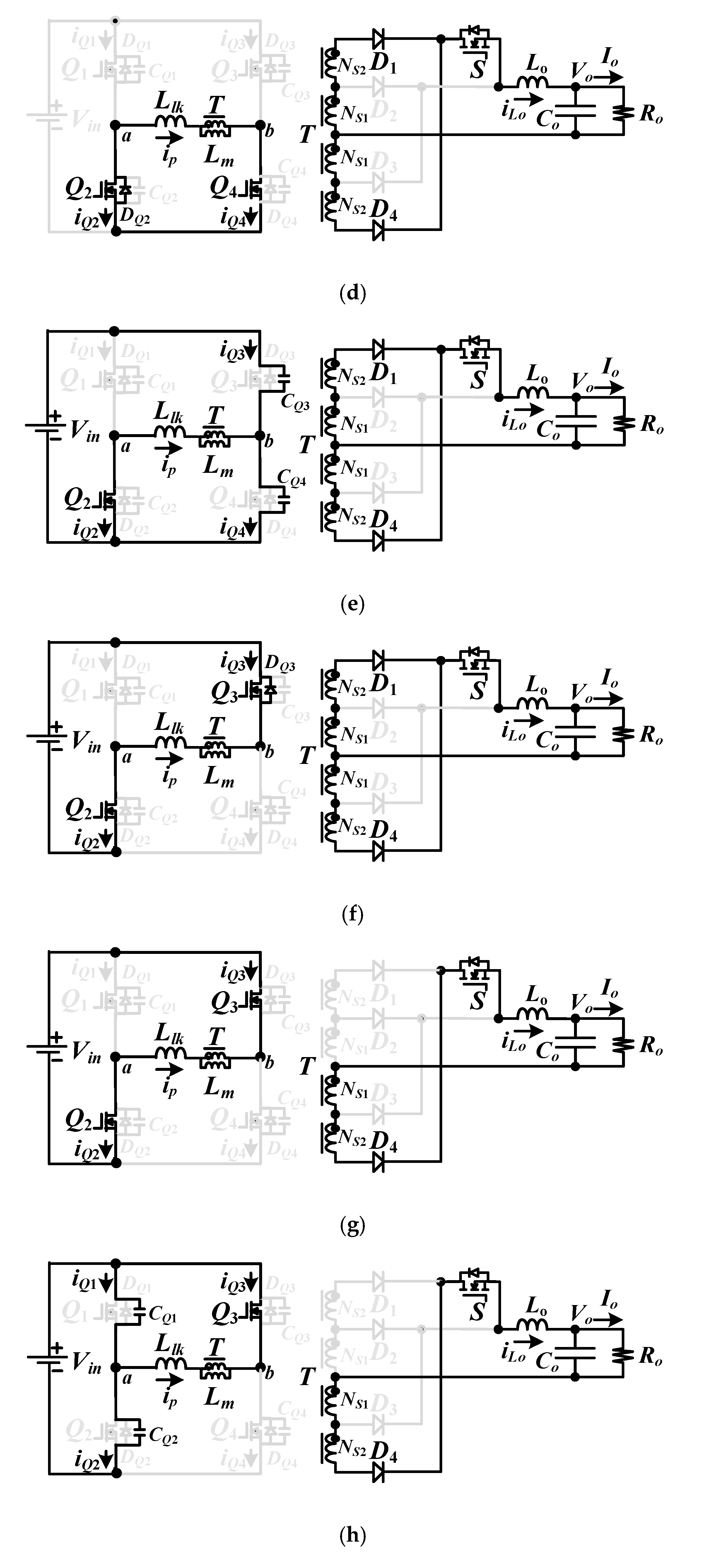
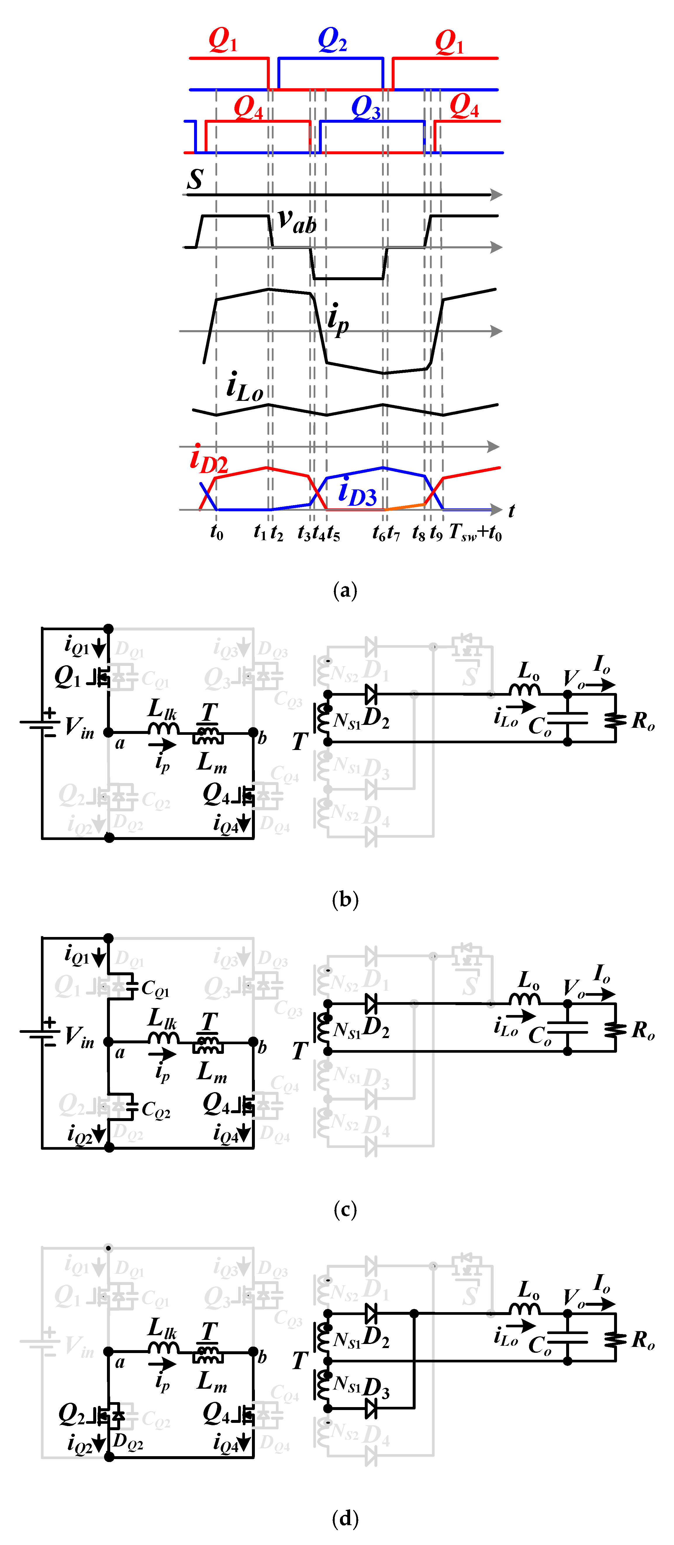
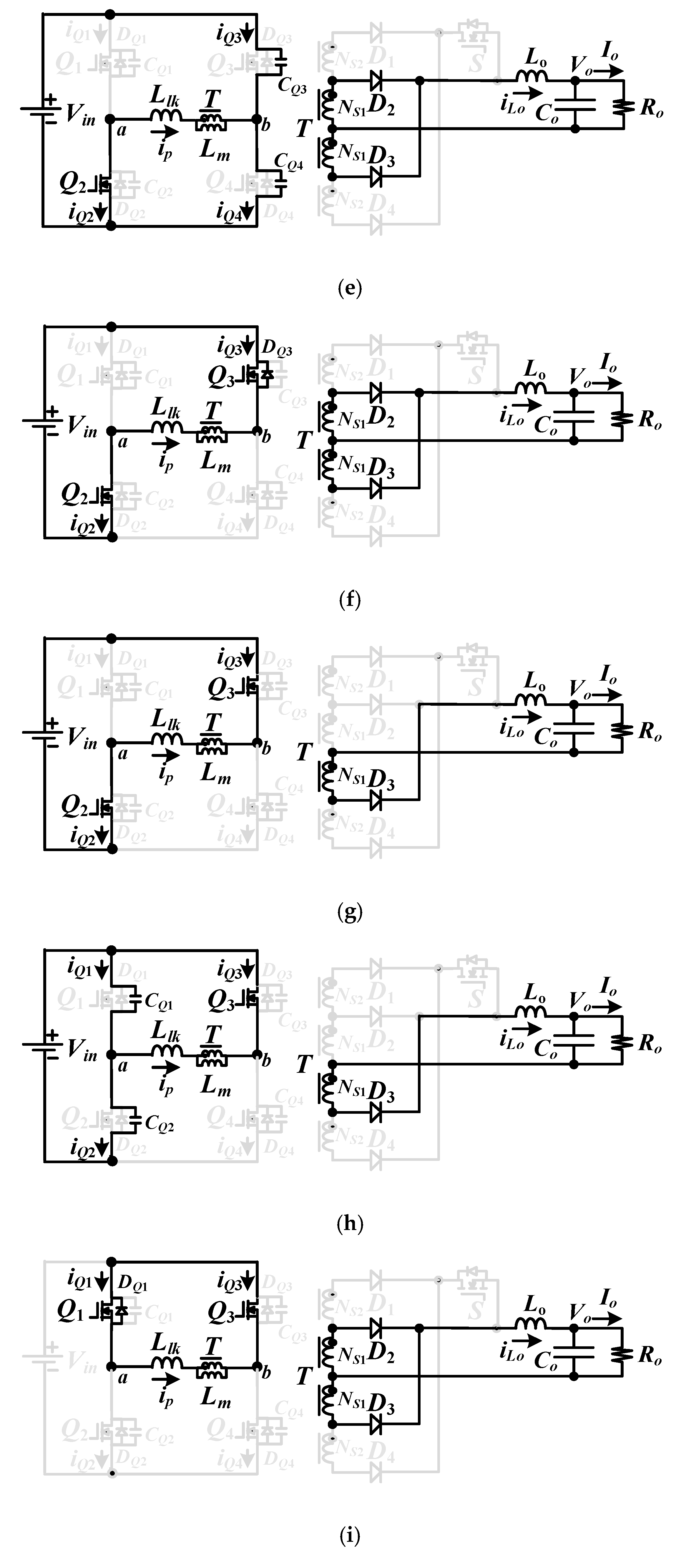
2. Circuit Structure

The proposed circuit with wide voltage operation is shown in Figure 1a. The basic structure of the studied circuit is a full-bridge circuit, Q1~Q4, Llk, and T, on input side and a center-tapped rectifier with two sets of secondary windings Ns1 and Ns2 and an auxiliary switch S on output side.
In relation to input voltage value, the studied circuit has two voltage operation ranges, low input voltage range and high input voltage range. When Vin is at low voltage range Vin = Vin,min~3Vin,min (3:1 operation range), the auxiliary switch S is in the on-state (Figure 1b). D2 and D3 are reverse biased. The secondary winding turns Ns1 + Ns2 are connected to output side. The turn-ratio of transformer T is Np/(Ns1 + Ns2) and the converter has higher dc voltage gain for low input voltage operation. The effective duty cycle of full-bridge converter is depended on input voltage value to maintain output voltage constant. PS-PWM scheme is used to control phase-shift angle between the lagging-leg and leading-leg. Therefore, the soft switching characteristics of power switches on full-bridge converter can be achieved. If Vin is at high voltage range Vin = 2Vin,min~6Vin,min (3:1 operation range), auxiliary switch S is in the off-state and D1 and D4 are off as shown in Figure 1c. The secondary turns Ns1 are connected to output side and the transformer turn-ratio is Np/Ns1. Thus, the presented circuit has lower dc voltage gain in high input voltage operation. Based on the on/off states of auxiliary switch S and winding turns Ns1 + Ns2 or Ns1 connected to output load, a soft switching full-bridge converter with 6:1 (Vin,max/Vin,min = 6) wide input voltage range is accomplished in the studied circuit.

3. Operation Principle

The duty cycle control is used to generate the proper switching signals and provide a stable output voltage against the variation of Vin and Io. According to input voltage value, auxiliary switch S is controlled at on-state or off-state for low voltage range operation or high voltage range operation. In the studied converter, it is assumed that Lm >> Llk, CQ1 = … = CQ4 = Coss and Ns1 = Ns2 = Ns. The proposed circuit has two input voltage ranges, Vin,min~3Vin,min and 2Vin,min~6Vin,min. The pulse-width modulation waveforms and the equivalent circuits for two input voltage ranges are provided in Figure 2 and Figure 3. For each input voltage range, the proposed circuit has ten modes in every switching cycle.

3.1. Low Voltage Range (S on)

When Vin,min < Vin < 3Vin,min, auxiliary switch S is turned on. The effective duty cycle deff of full-bridge circuit is related to input voltage. The transformer turn-ratio in low voltage range is nL = Np/(Ns1 + Ns2). The dc voltage gain is expressed as GL = Vo/Vin.L = 2deff/nL where Vin,L denotes Vin in low input voltage range. The pulse-width modulation waveforms are given in Figure 2a and the ten equivalent circuits for low voltage range operation are provided in Figure 2b–k.
Mode 1 [t0, t1]: In mode 1, Q1 and Q4 are on and vLmVin due to Lm >> Llk The power flow from input source to output load is through Llk, T, D1, Lo and Co. The output inductor voltage vLoVin/nLVo > 0 and iLo increases.
Mode 2 [t1, t2]: Q1 is off at time t1. Because of ip(t1) > 0, CQ2 (CQ1) is discharged (charged). Due to CQ1 and CQ2 are low capacitances, ip and iD1 are almost constant. At time t2, vCQ2 = 0 and the time duration in mode 2 is calculated as Δ t mode   2 2 V i n C o s s n L / i L o ( t 1 ) .
Mode 3 [t2, t3]: Since ip(t2) > 0 and vCQ2(t2) = 0, DQ2 conducts and Q2 turns on after t2 to have zero-voltage switching characteristic. In order to have soft switching operation, the dead time td between Q1 and Q2 is needed and expressed as t d > Δ t mode   2 = 2 V i n C o s s n L / i L o ( t 1 ) . Since Llk << Lm and Ron,sw (turn-on resistance of switches Q1 and Q2) is about hundreds of milliohm, the transformer primary voltage vLm and the secondary voltages vs,N1 and vs,N2 approximate zero voltage. D1 and D4 are forward biased. Then the inductor voltage vLo = −Vo and iLo decreases. The primary current i P ( t ) i P ( t 2 ) V Q 24 , d r o p / r l k where rlk is the equivalent resistance on Llk and VQ24,drop is voltage drop on Q2 and Q4.
Mode 4 [t3, t4]: At time t3, S4 is off. Because of ip(t3) > 0, CS3 (CS4) is discharged (charged). Due to CS3 and CS4 are low capacitances, ip, iD1 and iD4 are constant. At time t4, vCQ3 = 0. The time duration in mode 4 is calculated as Δ t mode   4 2 V i n C o s s / i p ( t 3 ) .
Mode 5 [t4, t5]: Because of ip(t4) > 0 and vCQ3(t4) = 0, DQ3 is forward biased and S3 turns on after t4 to have zero-voltage switching operation. Due to both D1 and D4 are conducting, the primary magnetizing voltage vLm is clamped at zero voltage. Thus, the leakage inductor voltage vLlk = −Vin and ip is decreased. In this mode, iD1 (iD4) is decreased (increased) to 0 (iLo) at time t5. The time duration in mode 5 is expressed as:
Δ t mode   5 = ( i p ( t 4 ) i p ( t 5 ) ) L l k / V i n 2 I o L l k / ( n L V i n )
The duty loss in Mode 5 is calculated in (2):
d l o s s , 5 2 I o L l k f s w / ( n L V i n )
The waveforms in modes 6–10 are symmetry to waveforms in modes 1–5. Therefore, the analysis and discussion of modes 6–10 are neglected in this section.

3.2. High Voltage Range (S off)

When 2Vin,min < Vin ≤ 6Vin,min, S is off and D1 and D4 are reverse biased as shown in Figure 1c. Only the secondary turns Ns1 are connected to output load and the turn-ratio of transformer in high voltage range is nH = Np/Ns1. The effective duty cycle deff depends on Vin and Io. The dc voltage gain in high voltage range operation is given as GH = Vo/Vin,H = 2deff/nH where Vin,H denotes Vin in high input voltage range. Since turn-ratio nH = 2nL due to Ns1 = Ns2, it can obtain GH = GL/2 under the same effective duty cycle deff. That means the proposed converter has high voltage gain in low input voltage range and low voltage gain in high input voltage range. The circuit waveforms in high voltage range operation are provided in Figure 3a and the ten equivalent circuits for high voltage range operation are illustrated in Figure 3b–k. The circuit operation in Figure 3b–k with the secondary winding turns Ns1 in high voltage range are similar to the circuit operations in low voltage range presented in previous section. Therefore, the circuit analysis of the presented circuit operated at high voltage range are ignored in this section.

4. Circuit Characteristics and Design Example

Full-bridge PS-PWM converter with auxiliary secondary turns is adopted in the studied circuit to accomplish wide input voltage range operation. The effective duty cycle between the lagging-leg and leading leg is regulated under the different input voltage value and load current. For low (high) input voltage range, switch S is on (off) and the winding turns Ns1 + Ns2 (Ns1) are connected to output terminal. The output voltage can be derived in (3) from flux balance theory on Lo:
V o = { 2 V i n , L n L ( d 2 L l k I o f s w n L V i n , L ) ,   S   on 2 V i n , H n H ( d 2 L l k I o f s w n H V i n , H ) ,   S   off
where d is duty cycle of leg voltage vab and d = deffdloss,5. The average value of output inductor current iLo equals Io. The voltage ratings of active switches Q1Q4 equal Vin,max. The voltage ratings of D1D4 and S are functions of Vin,max, nL and nH.
V D 1 ,   r a t i n g = V D 4 ,   r a t i n g 2 V i n , max / n L
V D 2 ,   r a t i n g = V D 3 ,   r a t i n g 2 V i n , max / n H
V S ,   r a t i n g V i n , max / n H
The average values of diode currents are ID1 = … = ID4 = Io/2 and IS,av = Io. The output inductance Lo approximates:
L o ( V i n , max / n H V o ) d e f f , min Δ i L o f s w
The duty loss in Mode 5 is related to the leakage inductance Llk. If the maximum duty loss is defined, then the leakage inductance Llk is calculated in (8):
L l k = n L d l o s s , 5 V i n , min 2 I o f s w
The proposed converter is designed with the following parameters: Vin = 150–25 V (6:1 ratio), Vo = 12 V, Io,rated = 25 A, Po = 300 W and fsw = 100 kHz. When Vin = 25–75 V (low input voltage range), auxiliary switch S is on to obtain a high voltage gain due to the secondary turns Ns1 + Ns2 are connected to output side. If Vin is increased and equal to 75 V, then switch S turns off and the converter is operated in high voltage range. The winding turns Ns1 are connected to output side. If the input voltage is decreased from 150 V to 50 V, then switch S turns on and the circuit is operated in low voltage range. Thus, the proposed converter works in high voltage range when Vin = 150–50 V. It is assumed the proposed converter has 85% efficiency at Vin,min = 25 V and 100% power under low voltage range. The maximum duty cycle of leg voltage vab at Vin,min = 25 V is assumed 0.45 and the assumed duty cycle loss dloss,5 = 0.08:
d l o s s , 5 = 2 I o L l k f s w / n L V i n , min = 0.04
From (3) and (9), the leakage inductance approximates:
L l k = η   d l o s s , 5   d max   V i n , min 2 P o   f s w 0.6375 μ H
From (3), the turn-ratio nL can be derived in (11):
n L d max V i n , min + ( d max V i n , min ) 2 4 V o L l k I o f s w V o 1.5
In the prototype circuit, transformer T is implemented using TDK (Tokyo Electric Chemical Industry Co., Ltd.) EER-42 ferrite core with winding turns Np = 12 and Ns1 = Ns1 = 4 and Lm = 400 μH. The minimum effective duty cycle deff,min at Vin,L,max = 75 V is derived in (12):
d e f f , min = d e f f , max V i n , L , min V i n , L , max = ( 0.45 0.08 ) × 25 75 0.123
The maximum ripple current ΔiLo at Vin,L,max = 75 V (low input voltage range) is assumed 30% of load current. From (7), the inductance Lo is expressed as:
L o ( V i n , L , max / n L V o ) d e f f , min Δ i L o f s w 6.23   μ H
The Lo = 8 μH is used in the prototype circuit. The rms (root-mean-square) currents of Q1Q4 are approximately calculated as:
i Q 1 , r m s = = i Q 4 , r m s = I o , r a t e d n L η 2 13.9   A
The maximum voltage on Q1Q4 is the maximum input voltage Vin,max = 150 V. The average diode currents ID1ID4 are 12.5 A. The voltage ratings of D1D4 are given in (15) and (16):
V D 1 ,   r a t i n g = V D 4 ,   r a t i n g 2 V i n , max / n L = 200   V
V D 2 ,   r a t i n g = V D 3 ,   r a t i n g 2 V i n , max / n H = 100   V
MOSFETs (metal–oxide–semiconductor field-effect transistor) IRFB4229 with 250 V/46 A ratings are adopted for active switch Q1~Q4 and IRF3145 with 150 V/30 A ratings is adopted for auxiliary switch S. Fast recovery diodes APT30DQ60BG with 600 V/30 A ratings are selected for D1D4 and the output capacitance Co = 2000 μF.

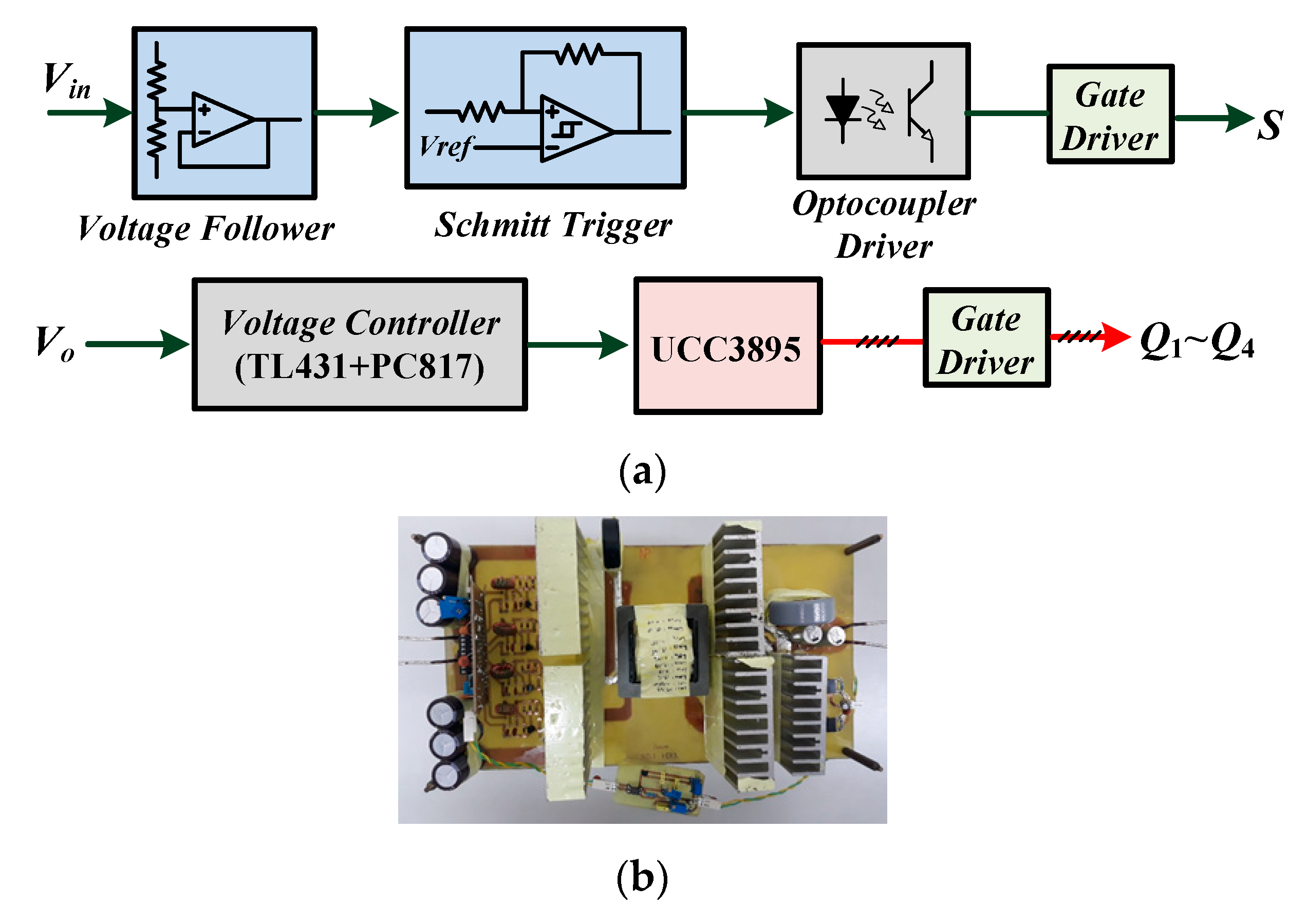
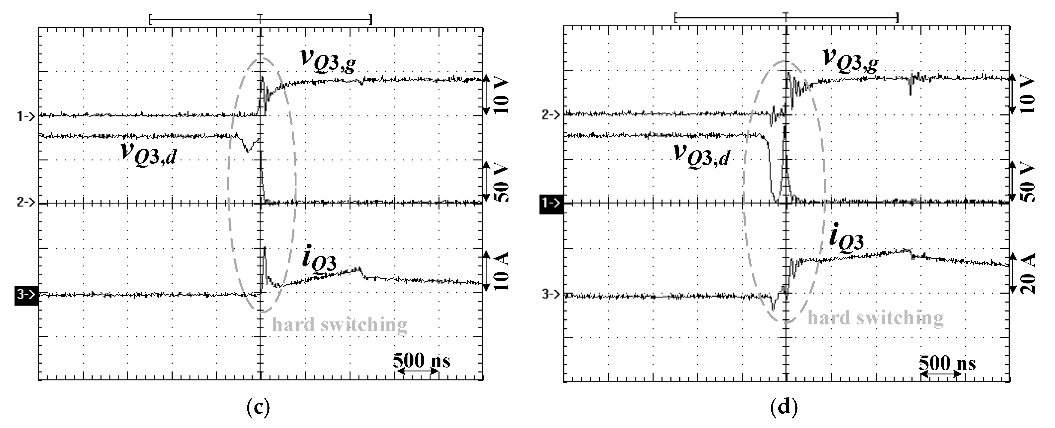
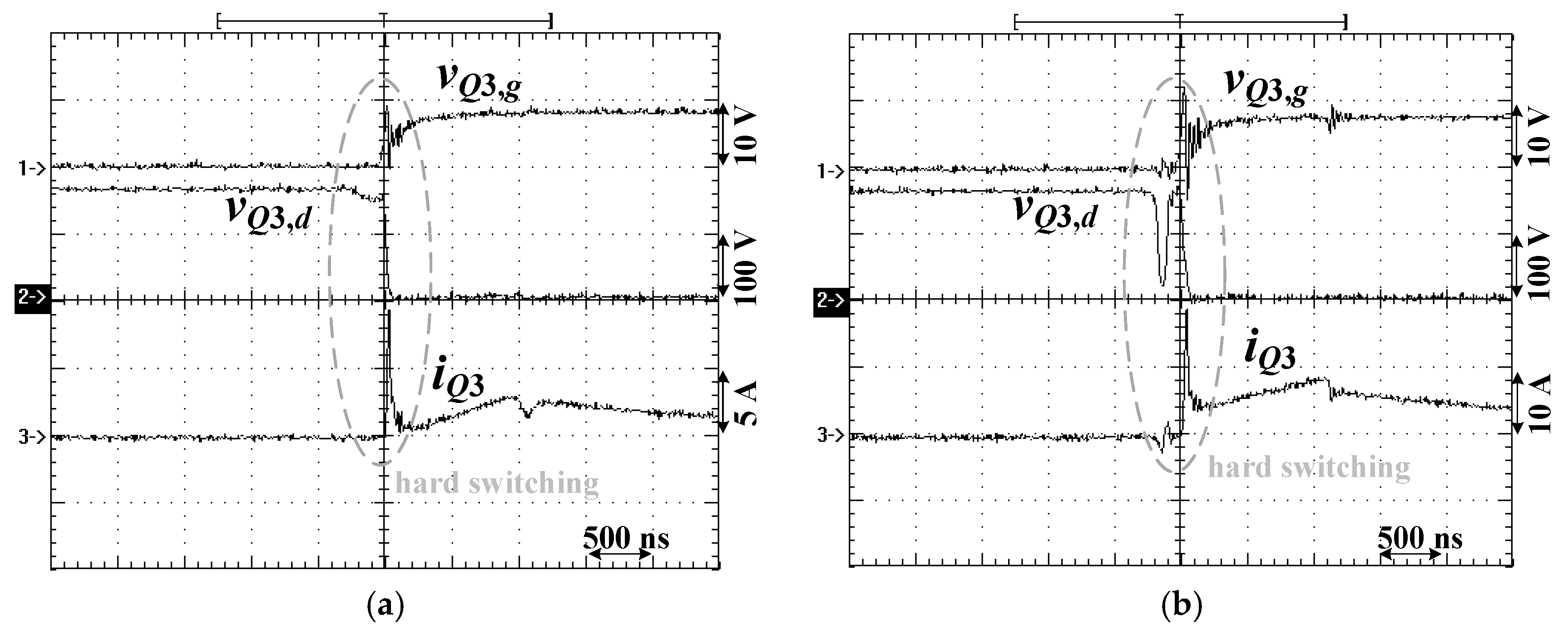
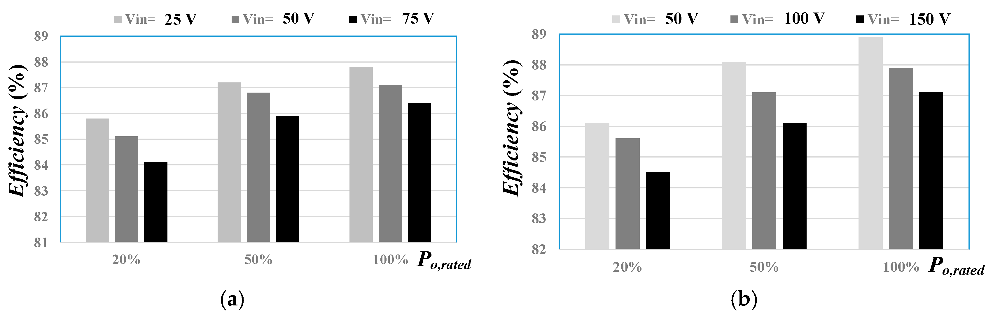
5. Simulated and Experimental Results

Figure 4a shows the control block of the signals Q1~Q4 and S. Schmitt trigger comparator is adopted to generate the signal S in order to select the correct range of input voltage. The PWM signals are generated by phase-shift PWM integrated circuit UCC3895. The output voltage is controlled by the voltage regulator TL431 and PC817. Figure 4b provides the photograph of the prototype. Figure 5 demonstrates the simulated results of the primary-side and the secondary-side voltages and currents at full load under low input voltage range for both Vin = 25 V and 75 V. One can observe that the effective duty cycle of vab at Vin = 25 V is larger than the duty cycle at Vin = 75 V. Therefore, the current ripple ΔiLo at Vin = 25 V is less than current ripple ΔiLo at Vin = 75 V. Similarly, the simulated results of the presented circuit operated at high input voltage range are provided in Figure 6 for both Vin = 150 V and 50 V. The lower input voltage (Vin = 50 V) has the larger duty cycle to reduce the output ripple current ΔiLo compared to the condition at Vin = 150 V case. Experiments from a prototype with circuit components derived from previous section are provides to demonstrate the converter performance. The proposed circuit is operated at low input voltage range when Vin is increased from 25 V to 75 V. Then, the circuit goes to the high input voltage mode. If the input voltage is decreased from 150 V to 50 V, then the circuit operation goes to low input voltage range. Based on the input voltage operation range. Figure 7, Figure 8 and Figure 9 gives the test results when input voltage is in low voltage range. Under low input voltage range, auxiliary switch S is on. Thus, the rectifier diodes D2 and D3 are reverse biased and off. Figure 7a,b show the experimental waveforms of the gate voltages, leg voltage vab and the primary current ip at Vin = 25 V and 75 V and the rated output. It is clear that the converter has less phase-shift between Q1 and Q4 and larger duty cycle on leg voltage vab at Vin = 25 V input. Figure 7c,d provides the test waveforms of iD1, iD4 and iLo at Vin = 25 V and 75 V and the rated power. Due the converter at Vin = 25 V input has large duty cycle, iLo has less current ripple at Vin = 25 V input compared to Vin = 75 V input. Figure 8a,b provides the experimental waveforms of switch Q1 in leading-leg at 20% and 100% loads under Vin = 25 V input. It is clear the soft switching operation of Q1 is achieved from 20% load under 25 V input case. In the same manner, test waveforms of Q1 at 20% and 100% loads under 75 V input are given in Figure 8c,d. It can observe that Q1 is also turned on at zero-voltage switching from 20% load at Vin =75 V input case. Switches Q1 and Q2 have the same turn-on/off characteristics in the leading-leg. Therefore, the soft switching operation of switches Q1 and Q2 at leading-leg can be accomplished from 20% load in low input voltage range operation. Figure 9a,b show the test waveforms of the switch Q3 at lagging-leg for 20% and 100% loads under 25 V input. It is clear that Q3 is also turned on at zero voltage switching from 20% load. Figure 9c,d provide the measured waveforms of Q3 at 75 V input. It can observe that Q3 is hard switching at 75 V input case for both 20% and 100% loads. The soft switching condition of power switches at lagging-leg (leading-leg) is related to the leakage inductor (output inductor). Normally, the leakage inductance is much less than the output inductance. Therefore, power switches at leading-leg have wide zero-voltage switching range compared to the lagging-leg switches. The test results shown in Figure 8 and Figure 9 agree with these statements. Figure 10, Figure 11 and Figure 12 gives the experimental waveforms of the proposed converter for high input voltage range operation at 150 V and 50 V input. The test waveforms of vQ1,g, vQ4,g, vab and ip at Vin = 150 V and 50 V under rated power are provided in Figure 10a,b. Compared to 150 V input case, the proposed converter has less phase-shift between Q1 and Q4 and larger duty cycle on leg voltage vab at Vin = 50 V input. The test results of iD1, iD4 and iLo at 100% load under 150 V and 50 V input are shown in Figure 10c,d. Figure 11 provides the experimental waveforms of leading-leg switch Q1 at various load power and input voltage values in high voltage range operation. It is clear that the soft switching operation of Q1 is accomplished from 20% load for both 150 V and 50 V input. Similarly, the test waveforms of lagging-leg switch Q3 at various load power and input voltage values are demonstrated in Figure 12. It can be observed that Q3 has soft switching operation only at 50 V input under 100% load and hard switching operation for the other conditions. Figure 13 provides the test results of the circuit efficiencies. For both low and high voltage range operation, the lower input voltage has larger effective duty cycle and less conduction losses on power switches compared to the higher input voltage. Thus, the circuit efficiency at 25 V input is better than 75 V input in low input voltage range. Similarly, the circuit efficiency at 50 V is better than 150 V input in high voltage range operation.

6. Conclusions

A full-bridge PS-PWM converter with auxiliary secondary turns is investigated to demonstrate the capability of 6:1 wide input voltage range operation for railway vehicle low power units and solar power converters. To achieve wide voltage range operation, two sets of secondary windings are used in the studied circuit. According to the different secondary winding turns connected to output terminal, there are two input voltage range operations in the converter. In each voltage range, the circuit can realize the 3:1 input voltage range operation. For low voltage range, the high transformer turns-ratio is adopted to achieve higher dc voltage gain. On the other hand, a low turns-ratio of transformer is used to obtain lower dc voltage gain of the studied circuit. Therefore, a 6:1 wide voltage operation is implemented in the presented converter. PS-PWM scheme is used to accomplish soft switching operation for leading-leg switches. The feasibility of the studied converter is verified and confirmed by a design example and some experiments in this paper.

Funding

This research is funded by the Ministry of Science and Technology, Taiwan, under grant number MOST 108-2221-E-224-022-MY2.

Acknowledgments

This research is supported by the Ministry of Science and Technology, Taiwan, under contract MOST 108-2221-E-224-022-MY2. The author would like to thank H. R. Cheng for his help to measure the circuit waveforms in the experiment.

Conflicts of Interest

The author declares no potential conflict of interest.

References

  1. Shang, C.; Liu, L.; Liu, M.; Men, S. A highly-efficient two-stage DC-DC converter with wide input voltage. In Proceedings of the 2015 IEEE International Telecommunications Energy Conference (INTELEC), Osaka, Japan, 18–22 October 2015; pp. 1–6. [Google Scholar]
  2. Zhou, G.; Ruan, X.; Wang, X. Input voltage feed-forward control strategy for cascaded DC/DC converters with wide input voltage range. In Proceedings of the 2016 IEEE 8th International Power Electronics and Motion Control Conference (IPEMC-ECCE Asia), Hefei, China, 22–26 May 2016; pp. 603–608. [Google Scholar]
  3. Jeong, Y.; Kim, J.K.; Lee, J.B.; Moon, G.W. An asymmetric half-bridge resonant converter having a reduced conduction loss for DC/DC power applications with a wide range of low input voltage. IEEE Trans. Power Electron. 2017, 32, 7795–7804. [Google Scholar]
  4. Wang, P.; Zhou, L.; Zhang, Y.; Li, J.; Sumner, M. Input-parallel output-series DC-DC boost converter with a wide input voltage range, for fuel cell vehicles. IEEE Trans. Veh. Technol. 2017, 66, 7771–7781. [Google Scholar] [CrossRef]
  5. Zhang, Y.; Fu, C.; Sumner, M.; Wang, P. A wide input-voltage range quasi-Z-source boost DC–DC converter with high-voltage gain for fuel cell vehicles. IEEE Trans. Ind. Electron. 2018, 65, 5201–5212. [Google Scholar] [CrossRef] [Green Version]
  6. Yao, Z.; Xu, J. A three-phase DC-DC converter for low and wide input-voltage range application. In Proceedings of the 2016 the IEEE Transportation Electrification Conference and Expo, Asia-Pacific (ITEC Asia-Pacific), Busan, Korea, 1–4 June 2016; pp. 208–213. [Google Scholar]
  7. Sunddararaj, S.P.; Rangarajan, S.S.; Gopalan, S. Neoteric Fuzzy Control Stratagem and Design of Chopper fed Multilevel Inverter for Enhanced Voltage Output Involving Plug-In Electric Vehicle (PEV) Applications. Electronics 2019, 8, 1092. [Google Scholar] [CrossRef] [Green Version]
  8. Lu, J.; Kumar, A.; Afridi, K.K. Step-down impedance control network resonant DC-DC converter utilizing an enhanced phase-shift control for wide-input-range operation. IEEE Trans. Ind. Appl. 2013, 54, 4523–4536. [Google Scholar] [CrossRef]
  9. Li, W.; Zong, S.; Liu, F.; Yang, H.; He, X.; Wu, B. Secondary-side phase-shift-controlled ZVS DC/DC converter with wide voltage gain for high input voltage applications. IEEE Trans. Power Electron. 2013, 28, 5128–5139. [Google Scholar] [CrossRef]
  10. Wang, X.; Tian, F.; Batarseh, I. High efficiency parallel post regulator for wide range input DC–DC converter. IEEE Trans. Power Electron. 2008, 23, 852–858. [Google Scholar] [CrossRef]
  11. Wu, H.; Wan, C.; Sun, K.; Xing, Y. A high step-down multiple output converter with wide input voltage range based on quasi two-stage architecture and dual-output LLC resonant converter. IEEE Trans. Power Electron. 2015, 30, 1793–1796. [Google Scholar] [CrossRef]
  12. Zong, S.; Fan, G.; Yang, X. Double voltage rectification modulation for bidirectional CLLLC resonant converter for wide voltage range operation. In Proceedings of the 2018 IEEE International Power Electronics and Application Conference and Exposition (PEAC), Shenzhen, China, 4–7 November 2018; pp. 1–6. [Google Scholar]
  13. Cha, H.; Peng, F.Z.; Yoo, D. Z-source resonant DC-DC converter for wide input voltage and load variation. In Proceedings of the 2010 International Power Electronics Conference - ECCE ASIA, Sapporo, Japan, 21–24 June 2010; pp. 995–1000. [Google Scholar]
  14. Kim, B.; Kim, S.; Hun, D.Y.; Choi, J.H.; Kim, M. Hybrid resonant half-bridge DC/DC converter with wide input voltage range. In Proceedings of the 2018 IEEE Applied Power Electronics Conference and Exposition (APEC), San Antonio, TX, USA, 4–8 March 2018; pp. 1876–1881. [Google Scholar]
  15. Lin, B.R.; Lin, G.H. Frequency-Controlled Current-Fed Resonant Converter with No Input Ripple Current. Energies 2018, 11, 1–13. [Google Scholar]
  16. Liu, B.; Jones, E.A.; Wang, F.F.; Zhang, Z.; Costinett, D.; Ren, R. Capacitor-clamped, three-level Gan-based dc-dc converter with dual voltage outputs for battery charger applications. IEEE J. Emerg. Sel. Top. Power Electron. 2016, 4, 841–853. [Google Scholar]
  17. Lin, B.R.; Wu, G.Y. Bidirectional Resonant Converter with Half-Bridge Circuits: Analysis, Design, and Implementation. Energies 2018, 11, 2450. [Google Scholar] [CrossRef] [Green Version]
  18. Antonio, J.B.; Barbi, I. Input-series and output-series connected modular output capacitor full-bridge PWM DC–DC converter. IEEE Trans. Ind. Electron. 2015, 62, 6213–6221. [Google Scholar]
  19. Lin, B.R.; Lin, G.H.; Jian, A. Resonant converter with voltage-doubler rectifier or full-bridge rectifier for wide-output voltage and high-power applications. Electronics 2019, 8, 3. [Google Scholar] [CrossRef] [Green Version]
Figure 1. Proposed 6:1 wide voltage range converter (a) circuit diagram (b) low voltage range operation (c) high voltage range operation.
Energies 13 00222 g001
Figure 2. Proposed converter for low input voltage range (a) pulse-width modulation waveforms (b) mode 1 circuit (c) mode 2 circuit (d) mode 3 circuit (e) mode 4 circuit (f) mode 5 circuit (g) mode 6 circuit (h) mode 7 circuit (i) mode 8 circuit (j) mode 9 circuit (k) mode 10 circuit.
Energies 13 00222 g002aEnergies 13 00222 g002bEnergies 13 00222 g002c
Figure 3. Proposed converter for high input voltage range (a) pulse-width modulation waveforms (b) mode 1 circuit (c) mode 2 circuit (d) mode 3 circuit (e) mode 4 circuit (f) mode 5 circuit (g) mode 6 circuit (h) mode 7 circuit (i) mode 8 circuit (j) mode 9 circuit (k) mode 10 circuit.
Energies 13 00222 g003aEnergies 13 00222 g003bEnergies 13 00222 g003c
Figure 4. Prototype circuit (a) control block of the signals S and Q1~Q4 (b) picture of the prototype.
Energies 13 00222 g004
Figure 5. Simulated results in low input voltage range and full load (a) primary side waveforms at 25 V input (b) primary side waveforms at 75 V input (c) secondary side waveforms at 25 V input (d) secondary side waveforms at 75 V input.
Energies 13 00222 g005
Figure 6. Simulated results in high input voltage range and full load (a) primary side waveforms at 150 V input (b) primary side waveforms at 50 V input (c) secondary side waveforms at 150 V input (d) secondary side waveforms at 50 V input.
Energies 13 00222 g006
Figure 7. Experimental results in low input voltage range and full load (a) primary side waveforms at 25 V input (b) primary side waveforms at 75 V input (c) secondary side waveforms at 25 V input (d) secondary side waveforms at 75 V input.
Energies 13 00222 g007
Figure 8. Experimental waveforms of the leading-leg switch Q1 in low input voltage range at (a) 25 V input and 20% load (b) 25 V input and 100% load (c) 75 V input and 20% load (d) 75 V input and 100% load.
Energies 13 00222 g008
Figure 9. Experimental waveforms of the lagging-leg switch Q3 in low input voltage range at (a) 25 V input and 20% load (b) 25 V input and 100% load (c) 75 V input and 20% load (d) 75 V input and 100% load.
Energies 13 00222 g009aEnergies 13 00222 g009b
Figure 10. Experimental results in high input voltage range and full load (a) primary side waveforms at 150 V input (b) primary side waveforms at 50 V input (c) secondary side waveforms at 150 V input (d) secondary side waveforms at 50 V input.
Energies 13 00222 g010
Figure 11. Experimental waveforms of the leading-leg switch Q1 in high input voltage range at (a) 150 V input and 20% load (b) 150 V input and 100% load (c) 50 V input and 20% load (d) 50 V input and 100% load.
Energies 13 00222 g011
Figure 12. Experimental waveforms of the lagging-leg switch Q3 in high input voltage range at (a) 150 V input and 20% load (b) 150 V input and 100% load (c) 50 V input and 20% load (d) 50 V input and 100% load.
Energies 13 00222 g012aEnergies 13 00222 g012b
Figure 13. Measured circuit efficiencies (a) in low input voltage range (b) in high input voltage range.
Energies 13 00222 g013

