Abstract
The endurance of polymeric insulation foil is investigated under a mixed medium-voltage stress (DC + medium-frequency rectangular pulse) by means of accelerated lifetime testing. A dedicated setup is used that allows us to selectively eliminate the known risk factors for premature insulation failure under medium-frequency pulse voltage stress: partial discharges (PDs) during pulse transitions, excessive dielectric heating, and systemic overvoltages. The obtained results on polyethylenterephtalat (PET) insulation foil suggest that the adequate consideration of these factors is sufficient for eliminating the adverse effects of the pulse modulation under the investigated conditions. Indeed, if all mentioned risk factors are eliminated, the time to failure observed under a pure DC stress is shorter than with a superimposed pulse (keeping the same peak voltage). There is then no indication of an additional detrimental “per pulse” degradation process (i.e., the time to failure is not dependent on pulse frequency). In contrast, when repetitive PDs are present, the lifetime under combined DC + rectangular pulse stress strongly decreases with increasing pulse switching frequency. PD erosion of the foil is quantified by means of confocal microscopy, and the applicability of the streamer criterion for predicting PD inception is discussed.
1. Introduction
Medium voltage (MV, ) power electronic converters based on medium-frequency (MF, ) energy conversion have stimulated numerous research efforts over the last years [1]. These converters, sometimes called Electronic Transformers or Solid State Transformers, use semiconductor switches to interface a power grid with a load or generator via a MF MV transformer (and other passive components). They thereby provide a galvanically isolated interface with controllable electric power flow between grids, loads, and generators of different voltage levels and frequencies (including DC). By employing switching frequencies of several kilohertz and beyond, these converters achieve significantly higher power densities (at equal efficiency) than their low-frequency (50 Hz) counterparts because the magnetic components scale approximately with the inverse of their operating frequency [1]. For these reasons, MV Electronic Transformers are expected to play a key role where actively controlled medium-voltage electrical energy conversion (AC-AC, AC-DC, DC-DC) is needed, or when space/weight constraints apply, such as in medium-voltage electric mobility and electric aircraft applications [2].
The maturing of wide band gap semiconductor technologies for power switching applications (SiC and GaN) considerably enlarges the design space for MF MV converters. In particular, switching losses can be reduced significantly by the increased switching speeds (> 10 kV/s) [3], and a further increase in conversion power density is possible by increasing the switching frequency (up to and beyond 100 ).
Increased switching speeds and frequencies, however, raise issues concerning the long-term endurance of organic insulation materials employed in MV converter systems [4,5]. The accelerated degradation and premature failure of insulation systems exposed to inverter-type medium voltages in the presence of partial discharge (PD) is a largely investigated topic [6,7,8,9,10], and PD is recognized as one of the main risk factors associated with this type of voltage stress:
- a.
- Enhanced partial discharge (PD) intensity. The number of PDs per unit of time is proportional to the switching frequency. In addition, PD amplitudes are observed to increase with switching speed [11]. Thus, if PD is incepted, the total PD charge and its erosive effect on the insulation material is greatly enhanced when switching frequency and speed are increased.
Moreover, it has been recognized early on [12] that the waveform and fundamental frequency of the voltage influence the (local) electric field stress to which the insulation materials are subjected. Thus, this constitutes another risk factor that must be considered when dealing with inverter-type voltages:
- b.
- Systemic overvoltages. The broad spectral content of the terminal voltage can excite system resonances, generate standing wave phenomena on electrically long conductors (cable/load impedance mismatch), and lead to strongly nonlinear voltage drops along windings or field-grading layers due to parasitic capacitive couplings [4]. As a result, the electric field stress on certain parts of the insulation can be increased significantly.
While premature failure under inverter-type voltages in the absence of PD is also documented in literature [13,14], the investigation of the associated (accelerated) aging mechanism(s) has not received as much attention as PD degradation under these voltage profiles. The negative impact of increased insulation temperature due to enhanced dielectric losses [15] is often cited as a possible cause for premature insulation failure under repetitive pulse stress in the absence of PD [7,9,10,16] and is certainly a risk factor to be considered in the insulation design:
- c.
- Excessive insulation temperature. Increased switching speeds broaden the spectral content of the terminal voltage, while a higher switching frequency shifts its frequency spectrum as a whole. Both effects typically entail enhanced dielectric losses. Losses associated with charge migration or the dielectric -relaxation have positive temperature coefficients and can lead to thermal runaway [17]. Moreover, increased capacitive currents can lead to significant heating of (field-grading) semiconductive layers [4]. Even in the absence of thermal runaway, a higher insulation temperature due to increased power (loss) densities enhances thermally activated degradation processes and—especially for organic materials—compromised (di)electric properties. Moreover, the problem of stress cracking and delamination is accentuated.
It has been shown [18] that (bulk) space charge evolves under inverter-type voltages that possess a DC offset (e.g., unipolar rectangular voltages). Thus, in addition to increased dielectric heating, several investigators also mention the possibility of space charge playing a role in premature failure, in particular, under DC-biased repetitive pulse voltages [19,20]. While it is well known that the distortion of the electrode field by space charges in the insulation bulk plays a key role under DC voltage stress [21], it remains unclear if the interaction of the highly dynamic electrode field with bulk space charge influences insulation aging, because the available studies do not allow to clearly separate the influence of dielectric losses from the potential influence of space charge. A further potential aging mechanism is thus proposed and its relevance for insulation failure under DC-biased repetitive pulse voltage stress investigated in this work:
- d.
- Space charge. Structural aging due to electromechanical stress from the Coulombic interaction between the highly dynamic electrode field (due to repetitive impulse voltages of high slew rate) with space charge evolving under the DC-component of the applied voltage.
The concept that the interaction of space charge with the electrode field and the associated electromechanical stress can lead to the aging of polymeric (especially semicrystalline) insulation materials is not new. The electromechanical force density (electrostriction omitted) acting on space charge is indeed a fundamental ingredient in several well-established microphysical models of dielectric aging, see [22,23,24,25]. While initially developed for DC voltage stress, the operant microphysical aging process (morphological changes such as the opening of sub-microvoids and crack propagation) can also be considered under AC or mixed (DC+AC) voltages. In this case, the deformation of the polymer structure (e.g., straining of polymer ties in the amorphous regions) will be modulated by the dynamics of the AC component of the electric field. It is argued in [26] (Chapter 6.6) that cyclic mechanical stress is expected to accelerate these processes because it causes the polymer chains to occupy conformational states that are more varied relative to the quasi-equilibrium states occupied under a constant electric field stress. Moreover, there is an additional mechanical energy dissipation (proportional to the excitation frequency) associated with the cyclic conformational changes.
It is thus expected that this mode of dielectric aging—if active at all—should be particularly pronounced when a DC voltage (promoting the creation of space charge) is modulated by a highly dynamic inverter-type voltage (i.e., with steep voltage fronts). At present, there is no lifetime data available in the literature on strictly unipolar repetitive impulse voltages that could help decide whether or not such an effect should be added to the list of risk factors when dealing with mixed voltages. Thus, in order to test this hypothesis, electrical endurance testing of polyethylenterephtalat (PET) insulation foils is performed under a DC medium-voltage stress superimposed by medium-frequency rectangular voltage impulses (Figure 1c). A dedicated setup is used which allows us to eliminate the known risk factors b. (overstressing due to voltage overshoot) and c. (excessive heating of the sample), as well as to study the transition from the PD-free to the PD regime (risk factor a.). The aim of this investigation is thus to contribute to an empirical basis that helps to decide on the question of completeness of the listed risk factors a. to c. for arbitrary inverter-type voltages.
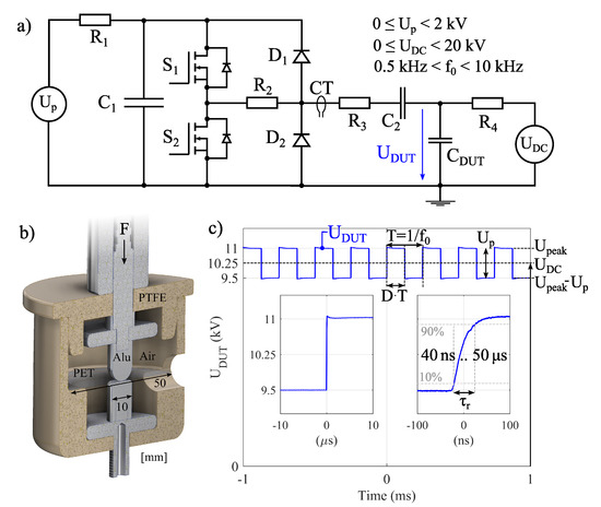
Figure 1.
(a) Schematic of mixed-frequency (DC + AC pulse) voltage generator; (b) electrode-specimen geometry; (c) exemplary pulse voltage waveform used for time-to-failure testing of polyethylenterephtalat (PET) foil in this study.
2. Methods
2.1. Test Bench
The simplified schematic of the MF pulse voltage generator (with variable DC-bias) constructed for the tests reported in this work is shown in Figure 1a. The pulse voltage is generated by a MOSFET half-bridge S1/S2 (Behlke HTS 21-07-HB-C) connected to the DC-bus capacitor and superimposed onto the DC voltage by capacitive coupling through . The DC voltage is applied to the sample through the = 1 resistor, which provides the necessary decoupling of the DC voltage source. Due to the AC-coupling, the DC component of the voltage is still given by . Choosing ensures that most of the pulse voltage drops across the specimen capacitance (test cell and voltage probe capacitance are understood to be included in the latter). The resistors = 220 and 50 along with the diodes and serve to protect the half-bridge in case of specimen breakdown (). The value of can be increased to decrease the slew rate of the pulse voltage fronts. The maximal slew rate (at ) is about 30 kV/μs.
In operation, the DC voltage drops across , and thus the output node of the half-bridge is pulled towards when the sample breaks down. The fast SiC diodes clamp this voltage rise by providing a discharge path for through ——— (for ) or ———— (for ), where is the breakdown impedance of the specimen. reduces the share of the breakdown current carried by the MOSFET body diodes. A current monitor (CT) detects this discharge current, blocks S1 and S2, and shuts down both voltage sources.
2.2. Sample Preparation and Electrode Geometry
Polyethylenterephtalat (PET) insulation foil (DuPont Melinex® S) is used for the voltage endurance tests. It is a semicrystalline polymer foil, commonly used in electrical applications as a capacitor dielectric or as a layer insulation in high-voltage transformers. The idea was to use a “typical, widely used” insulation material such that the obtained results are more likely to be representative for a larger group of polymeric insulation materials. The nominal thickness of the used foil is , and measured to be within 22.5 μm and 23.5 μm for all samples (all from the same reel). The foil is cut into circles of 50 mm diameter and stored in an air atmosphere with % RH and a temperature of for at least 12 prior to testing. Before the sample is placed in the sample holder, shown in Figure 1b, its surface is cleaned with ethanol and possible static charges are removed by contacting both sides with a conductive foil. The sample holder is then placed inside the test cell, which is at room temperature . A strong dependence of the time to failure on the air relative humidity (RH) was observed (not further investigated in this study). The RH inside the test chamber was thus held constant at % by a conditioned air purge flow (∼ 10 L min−1). At room temperature, the ingress of water molecules into a PET foil of 23 μm thickness is expected to reach the equilibrium concentration after a few minutes (estimation based on the diffusion length and the diffusion constant [27]). Controlling the RH inside the test cell is thus important when testing thin dielectric samples.
The high-voltage electrode (lower electrode in Figure 1b) is planar (diameter 10 mm with 1.5 mm fillet radius) while the ground electrode is a half-sphere of radius 5 mm. A spring mechanism generates a mechanical contact force to ensure a reliable and reproducible electrode contact. The electrostatic force between the electrode charges leads to an additional, voltage-dependent contribution to the contact force. From the Hertzian theory of elastic contact [28], with the extension proposed in [29] to include thin sheets of elastic materials on a rigid substrate (see Appendix A), the foil indentation depth is calculated to be at 11 kV ( at 0 kV), which corresponds to about 5 % of the foil thickness. The target insulation volume is thus localized underneath the indent of diameter . The foil is thus stressed with a quasi-homogeneous electrical field whose maximum is at the point of maximal indentation.
Outside of the indented region (near the triple point), the electrode potential is transferred to the polymer surface by means of partial discharges (PDs). If the repetitive pulses do not incept PDs, only the time-averaged voltage (i.e., the DC component) is transferred to the foil surface. Since all breakdown channels were located within the indented area, no attempt was made to quantify the lateral extent of the deposited surface charge layer.
The aluminum electrodes are removed and polished to a surface roughness of about () after each breakdown in order to eliminate the influence of metal protrusions generated by the breakdown channel. The surface roughness was estimated by means of confocal microscopy according to the international standard ISO 4287 (with Gaussian filter standard deviation ).
The PD inception voltage of the used electrode-specimen configuration is experimentally determined to lie between 1.0 and 1.1 kV . The sharp transition between the PD and non-PD regime can be well distinguished by means of an installed near-UV camera (∼ to ∼) and a photomultiplier tube (∼ to ∼). The inception voltage for repetitive PDs is determined only by the peak-to-peak value of the pulse voltage, but not the DC-bias . Indeed, the latter is eliminated within the air gap by an initial deposition of surface charges near the electrode contact area on the foil. The repetition rate of PDs due to DC stressing (i.e., not caused by the voltage transitions of the pulse modulation) is measured to be below 1 s−1 and its effect on insulation deterioration can thus be neglected (validated by microscopic inspection of the foil surface after stressing).
The described electrode-specimen configuration was chosen for the following reasons:
- The stressed volume is small, which allows to avoid a significant heating of the insulation even at high pulse frequencies (quantitative analysis given in Section 2.2.3), and thus to investigate insulation failure outside the thermal aging/thermal breakdown regime;
- The configuration has a high degree of (macroscopic) symmetry, and thus is more easily amenable to numerical estimations of system properties (thermal, electric field, etc.) than more complicated systems (such as twisted enamelled wires);
- The arrangement can be used to investigate the breakdown of polymeric insulation in the presence or absence of PDs without the need for replacing the surrounding air with insulating oil. This is a consequence of the well-defined insulator-electrode configuration and the associated existence of a narrowly scattered value of the inception voltage.
2.2.1. Test Procedure
The investigated voltage waveforms consist of a rectangular pulse train with a DC offset, as exemplified in Figure 1c. The test variable of main interest is the fundamental frequency of the pulse modulation. The pulse amplitude is also varied in order to study the transition from the PD-free to the PD regime. The pulse duty cycle D and the pulse rise/fall time are kept at and 40 , respectively, for all measurements presented here.
The DC offset voltage is adjusted to keep the nominal peak voltage at 11 for all tested values of pulse amplitudes (transient overvoltages are quantified in Section 3.2). The nominal peak voltage is given by
As mentioned at the end of the Introduction, the prime motivation for choosing this type of mixed-voltage stress (DC + repetitive pulse) is the provision of favorable conditions for the occurrence of the hypothesized additional “per pulse” aging mechanism (d.), such that its impact on insulation lifetime can be assessed empirically. In addition, lifetime data on insulation aging under this voltage profile is of direct practical interest for the high-voltage insulation design of Input Series Output Parallel (ISOP) DC-DC converters [30], gate drive auxiliary transformers of MV solid-state switches, as well as MV power module insulation.
At the beginning of a test, the pulse voltage is applied and the DC bias is ramped up to its final value within five seconds. This stress is then left unchanged until breakdown occurs. The time to failure is recorded automatically when the breakdown current detector triggers. All samples are visually inspected to ensure the presence of the breakdown puncture.
2.2.2. Statistical Analysis
The recorded time-to-failure (TTF) values are fitted by a two-parameter Weibull distribution, whose cumulative distribution function is given by
The fit is obtained by performing a least-square linear regression in the coordinate system within which all Weibull distributions appear as straight lines (see Figure 2). It is obtained by plotting as a function of .
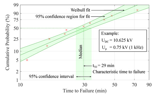
Figure 2.
Ten times to failure are recorded for each stress condition and fitted by a Weibull distribution. The corresponding median value and its 95 % confidence bound are given in Section 3.
The scale parameter is equal to the 0.63 percentile, while the shape parameter is a measure of the scatter of the TTF values around the median and is given by the slope of the regression line. Instead of the scale parameter, the 0.5 percentile (i.e., the median) will be used for the characteristic TTF values reported in the Results section. The 95% confidence interval for the median is obtained from the corresponding confidence bounds on the linear regression (the curved lines in Figure 2).
2.2.3. Maximal Sample Temperature
Although the present study is designed to not operate in a regime where the polarization losses due to the pulse voltage cause a significant insulation temperature rise, dielectric heating of the foil was analyzed in detail in order to ensure that this is indeed the case.
Details on the the derivation of the following expressions are given in Appendix B. For an excitation voltage of period T,
an upper bound on the maximal insulation temperature is shown to be the solution of the iterative scheme
where the (local) cooling coefficient () is a function of the geometry, the thermal conductivity of the foil, and the thermal resistance to the heat bath of temperature (electrodes). The spatial maximum of the dielectric loss density (, time-averaged over a period T) is given by
where is the DC conductivity and is the imaginary part of the effective dielectric permittivity (it includes the DC conductivity for the voltage components ).
3. Results
The results section starts out by showing that excessive insulation temperature can be excluded as a cause of insulation failure for the stress profiles and electrode configuration used in this study. Then, the measured characteristic TTF values (median and 95% confidence interval of the fitted Weibull distribution) are presented. It is shown that above a threshold value of the pulse modulation amplitude, repetitive PDs are present on the foil surface, leading to an insulation lifetime that decreases with increasing switching frequency. On the contrary, below PD inception (and in the absence of excessive dielectric heating as well as significant overvoltage), no accelerating influence of the switching transitions on insulation aging is observed.
3.1. Dielectric Heating
For (mixed) broadband voltages, the dielectric loss density is a convolution of the power spectrum and dielectric parameters, as given by Equation (5). For the numerical calculations, the effective dielectric permittivity was determined by dielectric spectroscopy on the actual PET foil samples used in the TTF testing. The following temperature parametrization of the DC conductivity of PET is used:
where and are derived from the high-field measurement data (up to 50 kV mm−1) provided in [31] by linear extrapolation to the maximal DC field strengths occurring here (∼400 kV mm−1). The maximum insulation temperature is determined with the formalism outlined in Section 2.2.3, by using worst-case estimates of the involved parameters (e.g., thermal coupling to electrodes). Of all the parameter combinations used in this study, the highest insulation temperature increase is obtained with , , , and equals about 3 °C. The conduction losses (first term in Equation (5)) are negligible at room temperature and cannot be activated by the temperature rise provoked by the AC dielectric losses. Based on this analysis, it is thus justified to exclude risk factor c. (Excessive insulation temperature) as a plausible cause of insulation failure in this study.
With a view to the typically more bulky insulation encountered in actual MV insulation systems, it is useful to keep in mind that the risk of a thermal instability (at fixed electric field stress) increases rapidly with insulation thickness d, because the cooling coefficient scales approximately as (see Appendix B, Equation (A19)). Moreover, the external losses from windings, magnetic core, semiconductors, etc. add to the increase in insulation temperature and feature positive temperature coefficients, thereby contributing to the risk of thermal insulation failure.
3.2. Systemic Overvoltages
Repetitive systemic overvoltages occurring at the switching transition are identified as a risk factor for accelerated insulation aging under inverter-type voltages (risk factor b. mentioned in the Introduction). It is therefore important to quantify the actual voltage overshoot present in the system used for insulation testing, because the actual repetitive peak voltage can be significantly higher than the nominal peak voltage derived from the DC link capacitor voltage (see Equation (1)). In this study, the combination of a low sample capacitance (<100 pF, including voltage probe and test cell parasitics) and low-inductive connections from the inverter output to the sample provides a negligible voltage overshoot (<5%) even at the shortest rise time (). Above , the overshoot is below 1%. Measurements of the output waveform were performed with a LeCroy PPE 20 / 100 high-voltage probe.
3.3. Partial Discharge Inception Voltage (PDIV)
The partial discharge inception voltage of the employed electrode-specimen configuration is experimentally determined to lie between and (for a duty cycle and hence ). The DC voltage component does not significantly influence the repetitive PDIV, since the associated component of the electric field is expelled from the air gap by an initial deposition of surface charges.
The presence of repetitive PDs leads to an erosion of the foil surface and a substantial reduction of the foil thickness. Figure 3a shows a confocal microscope image of the eroded area. The ring-shaped form of the eroded area is explained by the streamer criterion [32],
which states that the integral of the effective ionization coefficient along a field line from the electrode surface () to the edge of critical volume () must exceed a certain threshold value known as the streamer constant . The critical volume is the volume in which the effective ionization coefficient is positive, i.e., where electron avalanches can develop.
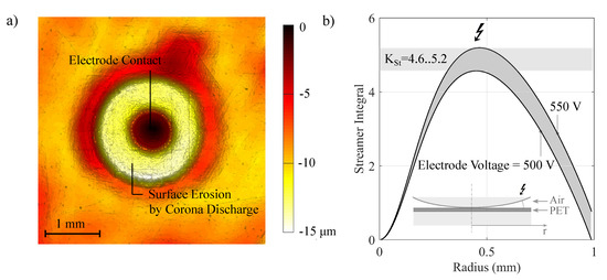
Figure 3.
(a) Confocal microscope image of PD-eroded foil surface and (b) streamer integral value for electrode voltages as a function of the radial base point position of the electric field line.
By using the parametrization of provided in [33], the streamer integral for the investigated geometry features a maximum value at , which agrees well with the measured erosion profile (Figure 3a). For , the integration path within the air gap is too short for a streamer discharge to develop, while at , the electric field along the field line is too weak to promote collision ionization. The value of the streamer constant predicting the observed PDIV lies in the range .
3.4. Times to Failure
The time to failure as a function of the pulse amplitude is shown in Figure 4. The peak voltage is kept at 11 kV. The switching frequency and the pulse rise/fall time are 4 kHz and 40 ns, respectively. It can be seen that the function presents a maximum around the PDIV. At the scatter is relatively larger, because some samples initiate PDs (with a corresponding lifetime shorter than for ) while others do not (with a lifetime longer than for ).
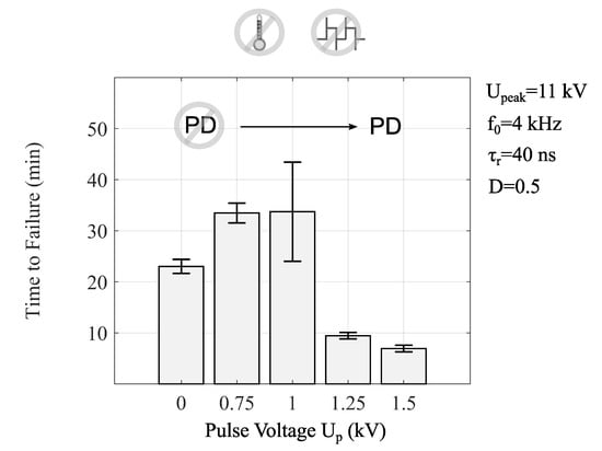
Figure 4.
Below partial discharge inception voltage (PDIV) (), the time to failure increases with increasing pulse voltage (at fixed peak voltage ). Above PDIV (), on the other hand, the lifetime decreases with increasing pulse voltage amplitude.
The times to failure scale very differently as a function of switching frequency in the PD and PD-free regime. Figure 5a shows that there is a clear “per pulse” degradation in the presence of PDs (). Quantitatively, the functional dependence is obtained by a least square polynomial fit, which indicates that the deterioration per pulse decreases with increasing switching frequency.
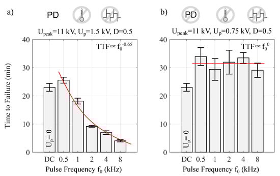
Figure 5.
Characteristic times to failure (median of the fitted Weibull distribution) under DC-biased pulse voltages as a function of pulse fundamental frequency: (a) A “per pulse” degradation is active when the pulse modulation is able to incept repetitive PDs. (b) On the contrary, in the absence of PD (as well as transient overvoltages and excessive dielectric heating), the measured insulation lifetime is not significantly dependent on the pulse frequency, and increased compared to a pure DC voltage of the same peak value. The fitted curves illustrate the calculated power function dependency of the characteristic time to failure on pulse frequency.
A completely different picture is observed when the pulses are unable to incept PDs (). As is shown in Figure 5b, the time to failure in this case is independent of the switching frequency (within statistical uncertainty), that is, . Moreover, the measured value of the time to failure is about 30% larger on average than for a pure DC voltage of the same peak value.
4. Discussion
Before entering into the discussion of the results, it seems appropriate to stress that the conclusions drawn from the empirical data of this study should not be transferred to other types of mixed-voltage stresses and other insulation systems—unless there is a physical reason to do so. Moreover, it is important to be aware of the inherent limitations of accelerated aging tests, e.g., that the relative importance of different aging mechanisms can change as a function of the applied stress level. Moreover, in actual insulation systems, other types of insulation stressors (e.g., mechanical and environmental) are present and need to be addressed for reliable insulation designs.
The main goal of this study was to find out if there is experimental evidence of an additional degradation/aging mechanism (d.) that is activated by superimposing a repetitive pulse voltage onto a DC bias voltage. The risk factors b. (Transient overvoltage) c. (Excessive insulation temperature) are excluded in this study.
Repetitive PDs occur when the pulse amplitude exceeds a certain threshold value, and their presence results in a drastic decrease of insulation lifetime with increasing switching frequency. This reduction in lifetime can be explained by the erosive effect of the PDs: confocal microscopy of the foil surface shows that polymer material is removed below the dielectric barrier discharge plasma to a substantial fraction of the foil thickness. This leads to a steady increase in the electric field stress in the remaining layer of insulation, until its breakdown strength is exceeded. The lifetime under varying pulse fundamental frequencies scales inversely with the average intensity of the light emission captured by the near-UV camera. This is in line with the previous conclusion of PD erosion being the culprit for faster insulation deterioration for increased pulse repetition frequencies.
The spatial extent of the PD region agrees well with mathematical modeling based on the streamer criterion. However, the obtained value of the streamer constant predicting the observed value of the PDIV is much lower () than the standard value traditionally used for determining streamer inception in air [34]. Similar low values () of the streamer constant are reported in the recent literature [35] on the investigation of PDIV for twisted pairs of enameled wire, where the electrode configuration and dimensions of the discharging air gap are similar to those occurring in the present study. The authors in [35] refer to literature that scrutinizes the value of the streamer constant, in particular, the relation , where is the critical number of electrons required to initiate the streamer propagation mode of the discharge: “there is no reason apart from tradition for retaining equal to 18” [36] (p. 729). There thus seems to be a need for better understanding the inception criteria of PD in dielectric-barrier-type electrode configurations under inverter-type medium voltages.
In the absence of PDs (as well as transient overvoltages and significant dielectric heating), there is no premature failure observable when modulating a DC voltage with a medium-frequency pulse voltage (keeping the same peak voltage). In fact, the results indicate that the physical processes leading to insulation failure under a pure DC voltage are merely modulated by the varying voltage levels. As expected in such a picture, the observed lifetime under a pure DC stress is shorter than with additional pulse modulation (because the average electric field stress is lower, and the pulse transitions do not negatively affect insulation lifetime). Accordingly, there is no dependence of the lifetime on pulse switching frequency. Thus, under the investigated conditions, there is no empirical evidence for an additional “per pulse” degradation mechanism beyond those considered in points a. to c. In particular, within the time scales investigated in this study, there is no evidence for the potential aging mechanism (d.) based on the cyclic electromechanical force exerted (by the repetitive voltage pulses) on space charge evolving under the DC field component of the applied stress. Although space charge was not quantified within this study, its presence under the applied level of DC field stress (in excess of 400 kV mm−1) is extremely likely, since space charge in PET foil has been measured at field strengths as low as 0.5 kV mm−1 [37].
5. Conclusions
The electrical endurance of PET insulation foil is investigated under DC-biased medium-frequency medium-voltage stress (DC + rectangular pulse). A sphere-plane electrode arrangement is employed, which takes care to eliminate transient overvoltages and excessive dielectric heating as causes of insulation failure. The following conclusions are drawn from the obtained results:
- PDIV is determined by the pulse peak-peak voltage , but not significantly influenced by the applied DC bias ;
- While the spatial extent of the PDs is correctly predicted by the streamer criterion, the application of the “textbook value” for the streamer constant () significantly overestimates the measured PDIV;
- Repetitive PDs erode the polymer surface (thinning of the foil) and breakdown occurs when the applied DC field exceeds the breakdown strength of the thinned foil;
- In the presence of PDs, the insulation lifetime shows a clear “per pulse” degradation, and it is typically shorter than under a pure DC voltage of the same peak amplitude;
- In the PD regime, the lifetime is inversely proportional to the optical PD intensity (as quantified by a near-UV camera) and scales as with the switching frequency. The “per pulse deterioration” thus decreases with increasing ;
- In the absence of PDs, no evidence is found of a detrimental “per pulse” impact on insulation lifetime (it is observed to be independent of the switching frequency in the investigated range). The processes leading to failure under a pure DC voltage are merely modulated by the changing voltage levels introduced by the rectangular pulse train. Accordingly, the lifetime with pulse modulation is observed to be larger than under pure DC voltage of the same peak amplitude.
Given the practical importance of accurate predictions of the PDIV in the design process of Type I insulation systems [6], future research will focus on the determination of PDIV as a function of geometry and all relevant material parameters, as well as waveform dynamics.
Author Contributions
Conceptualization, C.M.F., J.W.K., F.K., T.G., and R.F.; methodology, R.F.; software, T.G. and R.F.; validation, R.F.; formal analysis, R.F.; investigation, R.F.; resources, C.M.F., J.W.K, F.K., T.G., and R.F.; data curation, R.F.; writing—original draft preparation, R.F.; writing—review and editing, C.M.F., J.W.K, F.K., T.G., and R.F.; visualization, R.F.; supervision, C.M.F., J.W.K., and F.K.; project administration, C.M.F., J.W.K, F.K., T.G., and R.F.; funding acquisition, C.M.F., J.W.K., and F.K.
Funding
This project was carried out within the frame of the Swiss Centre for Competence in Energy Research on the Future Swiss Electrical Infrastructure (SCCER-FURIES) with the financial support of the Swiss Innovation Agency.
Acknowledgments
We thank M. Refaey and U. Straumann for their valuable comments on the manuscript. We acknowledge the service of ScopeM (Scientific Center for Optical and Electron Microscopy) at ETH Zürich for the confocal microscopy imaging.
Conflicts of Interest
The authors declare no conflict of interest.
Abbreviations
The following abbreviations and variables are used in this manuscript:
| AC | Alternating Current |
| DC | Direct Current |
| MF | Medium Frequency |
| MOSFET | Metal Oxide Field Effect Transistor |
| MV | Medium Voltage |
| PD | Partial Discharge |
| PDIV | Partial Discharge Inception Voltage |
| RH | Relative Humidity |
| TTF | Time To Failure |
| UV | Ultraviolet |
| d | Foil thickness (23 μm) | |
| Switching frequency | ||
| h | W m−2K−1 | Thermal interface conductance |
| k | W m−1K−1 | Thermal conductivity |
| — | Streamer constant | |
| °C | Temperature | |
| °C | Room temperature | |
| — | Effective dielectric permittivity | |
| S m−1 | DC conductivity | |
| Pulse rise/fall time | ||
| Pulse jump voltage | ||
| DC offset voltage |
Appendix A. Indentation of an Elastic Insulation Foil in a Sphere-Plane Electrode Configuration
Since the elastic modulus of aluminum () is much larger than that of PET (), it is justified to assume the electrodes to be nonelastic. According to the Hertzian theory of elastic contact [28], a rigid sphere of radius R indents a semi-infinite elastic medium (with ) and Poisson’s ratio by
where F is the applied contact force. The radius of the associated area of contact is given by . Waters [29] proposed a semiempirical extension of the Hertz model to include thin sheets of elastic materials on a rigid substrate:
where is an empirical constant. It can be seen that correction factor becomes relevant (<0.95) when the radius of the contact area approaches 10% of the foil thickness.
The contact force consists of the spring contact force and the voltage-dependent electrostatic attraction of the electrodes:
where is estimated on the basis of the formula for the geometric capacitance (in the limit ) presented in [38], i.e., using “force = partial derivative of the electrostatic energy with respect to electrode separation”:
Thus, the indentation depth is the solution of the equation
For R = 5 mm, d = 23 μm, , and = 3.2, the indentation depth is numerically determined to be
The electrostatic force adds a non-negligible fraction (45%) to the total electrode force, and the associated increase of the indentation depth amounts to about 20%. Moreover, the difference between and is very substantial, indicating that considering the indentation in a semi-infinite elastic half-space (i.e., without the correction factor introduced in Equation (A2)) would be inadequate.
Appendix B. Dielectric Heating: Estimation of Upper Limit on Temperature Rise
The goal of this section is to provide an an upper bound on the maximum temperature inside the PET foil (see Figure A1) for a specified excitation voltage and given material parameters. In order to simplify the mathematical treatment, a number of approximations that overestimate will be used. This will provide a formalism for determining an upper bound on , and hence for deciding under which conditions thermal breakdown does not occur.

Figure A1.
Enlarged view of the electrode contact area (PET foil on plane indented by half-sphere). The indented region () is shown on the left, while the right-hand side schematic depicts the area outside the indent (). The coefficients , , and are thermal contact conductances at the respective interfaces (unit: ). : PET-Aluminum contact in indented region; : cooling of foil surface to loosely contacting electrode surface; : cooling of foil surface by natural convection.

The temperature distribution inside the dielectric volume is determined by the balance of the heat generation and its transfer to the environment (a heat bath of temperature ). For the considered system, the steady-state temperature distribution is the solution of the boundary value problem
where is the thermal conductivity of PET, are the (outward-facing) surface normals at the insulation boundary , and are the thermal interface conductances. Worst-case estimates of the latter are derived based on the calculation procedures given in [39] and read
The heat source term for is given by
where is set to zero because the DC component of the electric field is assumed to be expelled from the air gap by the deposition of surface charge. The problem can be simplified to a one-dimensional treatment (i.e., no significant lateral thermal coupling), if the spatial variation of the heat source is small on length scales
For volume elements in the foil that are apart by more than , the thermal coupling to the heat bath is stronger than the thermal coupling between them. This simplification will be used, as Equation (A13) satisfies this condition reasonably well, and, in any case, the resulting peak temperatures are higher than those derived with a two-dimensional analysis that includes in-plane heat fluxes. Equation (A8) can thus be solved by considering heat fluxes along the vertical (z) axis only, i.e., as a one-dimensional boundary value problem (no in-plane heat fluxes). The sought-after maximum temperature occurs at some position with . If the local dielectric loss density is approximated by , the upper (u) and lower (d) foil surface temperatures read
Equation (A8) can be integrated to
The equation for finding thus reads
and can be solved iteratively:
The convergence of this iterative scheme implies the thermal stability of the sample. The higher-order corrections () take into account the temperature-dependence of the dielectric losses (through and ).
References
- Huber, J.; Kolar, J. Solid-State Transformers: On the Origins and Evolution of Key Concepts. IEEE Ind. Electron. Mag. 2016, 10, 19–28. [Google Scholar] [CrossRef]
- Rosero, J.; Ortega, J.; Aldabas, E.; Romeral, L. Moving towards a more electric aircraft. IEEE Aerosp. Electron. Syst. Mag. 2007, 22, 3–9. [Google Scholar] [CrossRef]
- Oswald, N.; Anthony, P.; McNeill, N.; Star, B. An Experimental Investigation of the Trade-Off between Switching Losses and EMI Generation with Hard-Switched All-Si, Si-SiC and All-SiC Device Combinations. IEEE Trans. Power Electron. 2013, 1, 8885–8993. [Google Scholar] [CrossRef]
- Bengtsson, T.; Dijkhuizen, F.; Ming, L.; Sahlen, F.; Liljestrand, L.; Bormann, D.; Papazyan, R.; Dahlgren, M. Repetitive fast voltage stresses-causes and effects. IEEE Electr. Insul. Mag. 2009, 25, 26–39. [Google Scholar] [CrossRef]
- Cigre Working Group D1.43. Insulation degradation under fast, repetitive voltage pulses. Techn. Brochure 2017, 2017, 703. [Google Scholar]
- IEC 60034-18-42. Rotating Electrical Machines—Part 18-42: Partial Discharge Resistant Electrical Insulation Systems (Type II) Used in Rotating Electrical Machines Fed from Voltage Converters—Qualification Tests; International Standard, Edition 1.0; International Electrotechnical Commission (IEC): Geneva, Switzerland, 2017. [Google Scholar]
- Wang, P.; Cavallini, A.; Montanari, G. The influence of repetitive square wave voltage parameters on enameled wire endurance. IEEE Trans. Dielectr. Electr. Insul. 2014, 21, 1276–1284. [Google Scholar] [CrossRef]
- Moonesan, M.; Jayaram, S.; Cherney, E. Time to failure of medium-voltage form-wound machine turn insulation stressed by unipolar square waves. IEEE Trans. Dielectr. Electr. Insul. 2015, 22, 3118–3125. [Google Scholar] [CrossRef]
- Yin, W. Failure mechanism of winding insulations in inverter-fed motors. IEEE Electr. Insul. Mag. 1997, 13, 18–23. [Google Scholar] [CrossRef]
- Kaufhold, M. Failure mechanism of the interturn insulation of low voltage electric machines fed by pulse controlled inverters. In Proceedings of the 1995 Conference on Electrical Insulation and Dielectric Phenomena, Virginia Beach, VA, USA, 22–25 October 1995; pp. 254–257. [Google Scholar] [CrossRef]
- Hammarström, T.J.; Bengtsson, T.; Blennow, J.; Gubanski, S. Partial discharges in motor wires at PWM voltages of different smoothness. In Proceedings of the 2014 International Symposium on Electrical Insulating Materials, Niigata, Japan, 1–5 June 2014; pp. 184–187. [Google Scholar] [CrossRef]
- Daugherty, R.; Wennerstrom, C. Need for industry standards for AC induction motors intended for use with adjustable-frequency controllers. IEEE Trans. Ind. Appl. 1991, 27, 1175–1185. [Google Scholar] [CrossRef]
- Fabiani, D.; Montanari, G. The effect of voltage distortion on ageing acceleration of insulation systems under partial discharge activity. IEEE Electr. Insul. Mag. 2001, 17, 24–33. [Google Scholar] [CrossRef]
- Koltunowicz, T.; Cavallini, A.; Djairam, D.; Montanari, G.; Smit, J. The influence of square voltage waveforms on transformer insulation break down voltage. In Proceedings of the 2011 Annual Report Conference on Electrical Insulation and Dielectric Phenomena, Cancun, Mexico, 16–19 October 2011; pp. 48–51. [Google Scholar] [CrossRef]
- Sonerud, B.; Bengtsson, T.; Blennow, J.; Gubanski, S. Dielectric heating in insulating materials subjected to voltage waveforms with high harmonic content. IEEE Trans. Dielectr. Electr. Insul. 2009, 16, 926–933. [Google Scholar] [CrossRef]
- Niayesh, K.; Gockenbach, E. On the aging mechanism of solid insulating materials exposed to repetitive high voltage pulses. IEEE Trans. Dielectr. Electr. Insul. 2014, 21, 304–310. [Google Scholar] [CrossRef]
- Guillod, T.; Färber, R.; Rothmund, D.; Krismer, F.; Franck, C.M.; Kolar, J.W. Dielectric Losses in Dry-Type Insulation of Medium-Voltage Power Electronic Converters. IEEE J. Emerg. Select. Top. Power Electron. 2019. [Google Scholar] [CrossRef]
- Fabiani, D.; Montanari, G.; Cavallini, A.; Mazzanti, G. Relation between space charge accumulation and partial discharge activity in enameled wires under PWM-like voltage waveforms. IEEE Trans. Dielectr. Electr. Insul. 2004, 11, 393–405. [Google Scholar] [CrossRef]
- Hudon, C.; Amyot, N.; Lebey, T.; Castelan, P.; Kandev, N. Testing of low-voltage motor turn insulation intended for pulse-width modulated applications. IEEE Trans. Dielectr. Electr. Insul. 2000, 7, 783–789. [Google Scholar] [CrossRef]
- Gao, B.; Wu, G.; He, J.; Lei, K. Investigation on aging mechanism of winding insulation used in inverter-fed traction motors. In Proceedings of the 2007 Annual Report—Conference on Electrical Insulation and Dielectric Phenomena, Vancouver, BC, Canada, 14–17 October 2007; pp. 107–111. [Google Scholar]
- Hanley, T.; Burford, R.; Fleming, R.; Barber, K. A general review of polymeric insulation for use in HVDC cables. IEEE Electr. Insul. Mag. 2003, 19, 13–24. [Google Scholar] [CrossRef]
- Jones, J.; Llewellyn, J.; Lewis, T. The contribution of field-induced morphological change to the electrical aging and breakdown of polyethylene. IEEE Trans. Dielectr. Electr. Insul. 2005, 12, 951–966. [Google Scholar] [CrossRef]
- Zeller, H.; Schneider, W. Electrofracture mechanics of dielectric aging. J. Appl. Phys. 1984, 56, 455–459. [Google Scholar] [CrossRef]
- Crine, J.; Parpal, J.; Lessard, G. A model of aging of dielectric extruded cables. In Proceedings of the 3rd International Conference on Conduction and Breakdown in Solid Dielectrics, Trondheim, Norway, 3–6 July 1989; pp. 347–351. [Google Scholar] [CrossRef]
- Dissado, L.; Mazzanti, G.; Montanari, G. The role of trapped space charges in the electrical aging of insulating materials. IEEE Trans. Dielectr. Electr. Insul. 1997, 4, 496–506. [Google Scholar] [CrossRef]
- Blythe, A.; Bloor, D. Electrical Properties of Polymers, 2nd ed.; Cambridge University Press: Cambridge, UK, 2005. [Google Scholar]
- Yasuda, H.; Stannett, V. Permeation, solution, and diffusion of water in some high polymers. J. Polym. Sci. 1962, 57, 907–923. [Google Scholar] [CrossRef]
- Timoshenko, S.; Goodier, J. Theory of Elasticity, 3rd ed.; McGraw-Hill: New York, NY, USA, 1982. [Google Scholar]
- Waters, N. The indentation of thin rubber sheets by spherical indentors. Br. J. Phys. 1965, 16, 557–563. [Google Scholar] [CrossRef]
- Fan, H.; Li, H. High-Frequency Transformer Isolated Bidirectional DC–DC Converter Modules With High Efficiency Over Wide Load Range for 20 kVA Solid-State Transformer. IEEE Trans. Power Electron. 2011, 26, 3599–3608. [Google Scholar] [CrossRef]
- Montanari, G.C.; Ghinello, I.; Motori, A.; Das Gupta, D. An investigation of conduction mechanisms at high-field in PET. In Proceedings of the IEEE 1997 Annual Report Conference on Electrical Insulation and Dielectric Phenomena, Minneapolis, MN, USA, 19–22 October 1997; Volume 2, pp. 451–454. [Google Scholar]
- Schumann, W. Über das Minimum der Durchbruchfeldstärke bei Kugelelektroden. Electr. Eng. 1923, 12, 593–608. [Google Scholar] [CrossRef]
- Zaengl, W.; Petcharaks, K. Application of Streamer Breakdown Criterion for Inhomogeneous Fields in Dry Air and SF6; Gaseous Dielectrics, VII; Christophorou, L.G., James, D.R., Eds.; Springer: Boston, MA, USA, 1994. [Google Scholar]
- Küchler, A. High Voltage Engineering; Springer: Berlin, Germany, 2018. [Google Scholar]
- Lusuardi, L.; Cavallini, A.; de la Calle, M.G.; Martínez-Tarifa, J.M.; Robles, G. Insulation design of low voltage electrical motors fed by PWM inverters. IEEE Electr. Insul. Mag. 2019, 35, 7–15. [Google Scholar] [CrossRef]
- Pedersen, A. On the electrical breakdown of gaseous dielectrics-an engineering approach. In Proceedings of the Conference on Electrical Insulation and Dielectric Phenomena, Leesburg, VA, USA, 29 October–2 November 1989; pp. 21–58. [Google Scholar] [CrossRef]
- Neagu, E.; Dias, C. Charge injection/extraction at a metal-dielectric interface: Experimental validation. IEEE Electr. Insul. Mag. 2009, 25, 15–22. [Google Scholar] [CrossRef]
- Crowley, J. Simple Expressions for Force and Capcitance for a Conductive Sphere near a Conductive Wall. In Proceedings of the ESA Annual Meeting on Electrostatics, Minneapolis, MN, USA, 17–19 June 2008. [Google Scholar]
- Bahrami, M.; Yovanovich, M.; Culham, J. Thermal Joint Resistances of Nonconforming Rough Surfaces with Gas-Filled Gaps. J. Thermophys. Heat Transf. 2004, 18, 326–332. [Google Scholar] [CrossRef]


© 2019 by the authors. Licensee MDPI, Basel, Switzerland. This article is an open access article distributed under the terms and conditions of the Creative Commons Attribution (CC BY) license (http://creativecommons.org/licenses/by/4.0/).