1. Introduction
Light emitting diode (LED) lighting has become more popular in recent years, particularly as product energy efficiency has become more important to consumers [
1,
2,
3]. Compared with conventional lighting equipment, LEDs are brighter and have a longer service life. LEDs have thus been used in various lighting scenarios, such as street lighting, indoor lighting, and backlighting. They have also been used for lighting equipment with high power requirements, like baseball field or basketball court lights. Most of these LED driver circuits have a two-stage architecture consisting of a power factor correction converter in the first stage and an isolated buck converter in the second stage, with an LLC resonant converter usually employed as the second-stage circuit [
4,
5].
Unlike other common isolated buck converters, an LLC resonant converter is characterized by power components with zero voltage switching (ZVS) and zero current switching at the high—and low—voltage ends, respectively, in a full load range. Additionally, unlike phase-shifted full-bridge converters, an LLC converter has no output inductance at the low-voltage end and thus has higher conversion efficiency [
6]. Moreover, to achieve high power density, increasing the switching frequency of the power switch reduces the volume of the magnetic component; however, this is accompanied by a considerable increase in switching loss. Therefore, in addition to the ZVS feature of the LLC resonant converter, wide-band-gap switch components should also be employed to reduce the switching loss under high-frequency operation [
7,
8]. Additionally, selecting an appropriate LLC resonant converter architecture can further optimize the efficiency and reduce component stress [
9,
10,
11]. The topologies commonly used in the high-voltage end of the LLC resonant converter are the half bridge and full bridge, whereas those used in the low-voltage end are the full bridge or center tap.
To achieve high power density, the leakage inductance of the transformer in this study was used as the resonant inductor of the circuit [
12,
13,
14], which reduces the number of magnetic components required. Previous research replaced the resonant inductor with the leakage inductance of the transformers, mostly through winding the transformer using litz wire and setting the operating frequency between 50 and 200 kHz. However, when the operating frequency is between 500 kHz and 1 MHz, the litz wire is usually replaced by printed circuit board (PCB) windings to reduce the alternating-current (AC) resistance of the copper traces under high-frequency operation. Additionally, the primary- and secondary-side windings are interleaved to weaken the proximity effect. This approach reduces proximity-effect-induced loss and minimizes the leakage inductance of the transformer [
15,
16,
17], which is a disadvantage in LLC resonant converters that require leakage inductance to design resonant tanks. A conventional method for increasing the leakage inductance is to increase the spacing between the primary and secondary sides [
18,
19,
20], which is mostly achieved using a non-interleaved winding that leads to a sharp rise in the proximity-effect-induced AC loss. Therefore, the concept of adjustable leakage inductance [
21,
22] was adopted in this study, with an additional reluctance length added between the primary-side and secondary-side windings of the transformer. This enabled the magnetic flux generated by the primary-side winding to flow into the added reluctance length, thereby increasing the primary-side leakage inductance. The proposed approach weakens the proximity effect in the interleaved winding and attains the objective of increasing the leakage inductance. Compared to existing LED power converter designs [
23,
24,
25], this work reduces the switching loss via wide bandgap devices and soft switching techniques under 500 kHz switching frequency conditions and utilizes an integrated transformer without an additional resonant inductor to achieve high power density. Ultimately, an LLC resonant converter with an output power of 1 kW, switching frequency of 500 kHz, input voltage of 400 V, and output voltage of 300 V was achieved in this study.
In this study, a second-stage LLC resonant converter was proposed for the LED driver circuit, and the LLC resonant circuit was used as a direct-current transformer (DCX) to operate the driver circuit at high efficiency. In addition, this study also designed and optimized the primary- and secondary-side topologies and magnetic components in the LLC resonant converter. In
Section 2, under the conditions of 1 kW output power, 400 V input voltage, and 300 V output voltage, the loss and component stress at the primary—and secondary—side structures of the converter are analyzed and a topology suitable for the specification in this study is selected.
Section 3 details the mathematical induction of adjustable leakage inductance and the appropriate number of primary- and secondary-side windings for the new core based on the optimal point of core loss and copper loss. The feasibility of the designed core structure was verified using ANSYS Maxwell software (ANSYS, Canonsburg, PA, USA).
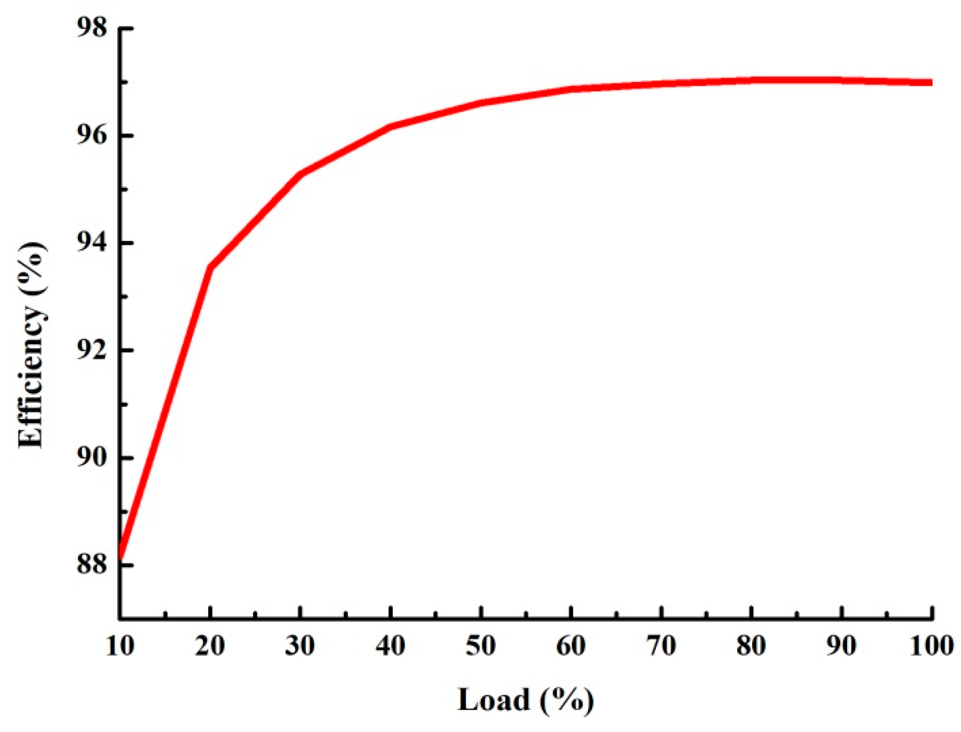
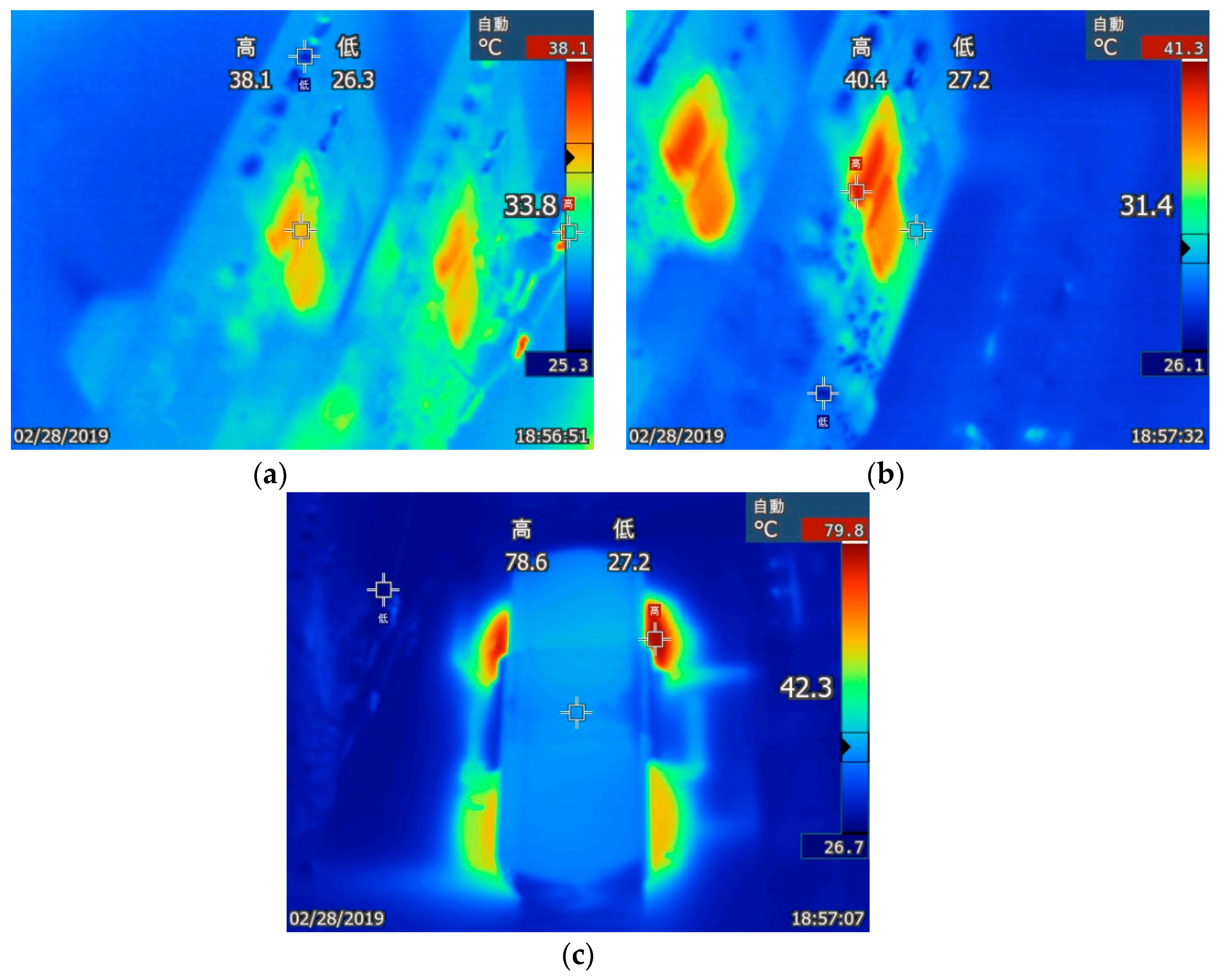
Section 4 presents the experimental results, including temperature distribution maps.
2. LLC Topology Comparison
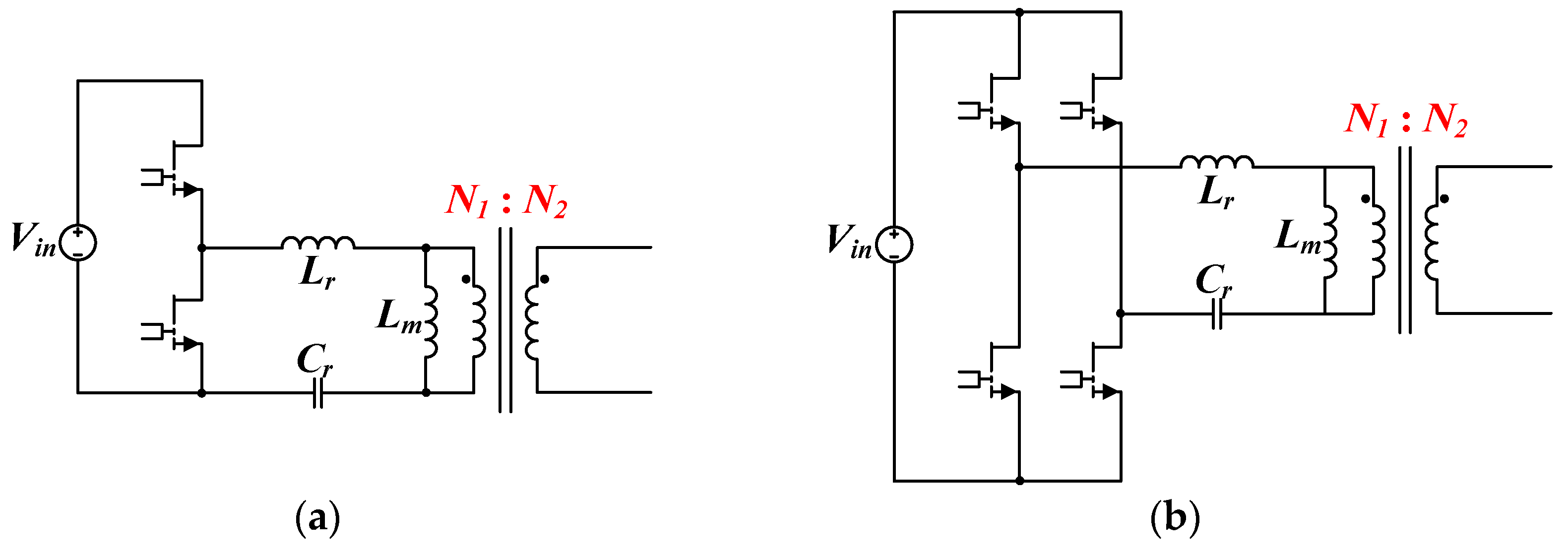
The primary and secondary sides of different architectures are discussed in this section. Because different circuit specifications have their appropriate architecture, the architecture is chosen based on power level and component stress, as shown in
Figure 1. The primary side may consist of a half bridge or full bridge, whereas the secondary side comprises a center-tap and full-bridge rectification. The choice of different architectures for the primary side results in different transformer designs; hence, the primary side is mainly selected based on the corresponding architecture for the appropriate power level. As for the different architectures on the secondary side, there are different component stresses and numbers of switches. Therefore, the appropriate architecture for the secondary side is mainly selected according to the level of the output voltage and current.
The common structures for the primary side are the half bridge and full bridge (
Figure 2). For the half bridge, the voltage across the resonant tank is +
Vin to 0 V; however, the actual voltage across the transformer is ±
Vin/2. Therefore, the turns ratio between the primary and secondary sides must be accounted for when designing the transformer. The energy transfer formula in Equation (1) can be rewritten as a general formula that establishes ZVS under a half-bridge structure, as shown in Equation (2).
in which the unit of
L is Henry (H),
I is Ampere (A),
C is Farad (F), and
V is Volt (V).
in which the unit of
Lm is Henry (H),
tdead is seconds (s),
Coss is Farad (F), and
fsw is Hertz (Hz).
For a full-bridge structure, the voltage across the transformer is approximately ±
Vin, and the input voltage can be directly divided by the output voltage to obtain the turns ratio when designing the transformer. For primary-side switching to achieve ZVS in a full-bridge structure, the energy transfer formula Equation (1) can be rewritten as the following general formula:
Under the conditions of 400 V input voltage, 300 V output voltage, and a half-bridge structure of the primary side, the equivalent turns ratio of the primary and secondary sides is indicated by Equation (4), whereas Equation (5) obtains the equivalent turns ratio of the two sides when a full-bridge structure is adopted on the primary side. In choosing the primary-side architecture, the conditions of primary-side ZVS are influenced by the stray capacitance [
26]. In particular, the stray capacitance of the secondary side mapped back to the primary side is affected by the turns ratio. Thus, if a half-bridge structure was adopted under this specification, the stray capacitance mapped from the secondary to the primary side would be magnified. Therefore, a full-bridge structure was employed in this study to reduce the effect on ZVS condition.
Table 1 [
27] shows a comparison of the various ratings of the two primary-side architectures.
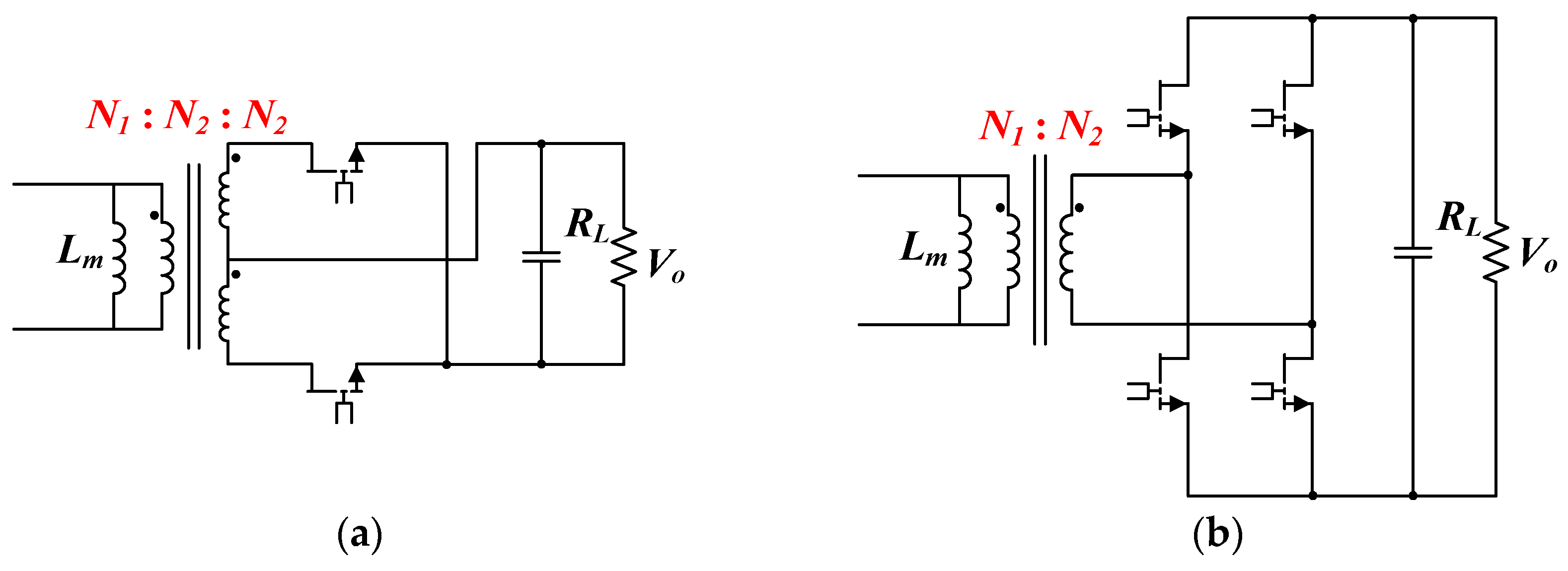
Common structures for the secondary side are center-tap and full-bridge rectification (
Figure 3). For center-tap rectification, the voltage over the secondary side of the transformer was 1 ×
Vo; however, the voltage over the synchronous rectifiers (SRs) was 2 ×
Vo, and overall, the conduction loss amounted to that of two SRs. Based on this analysis, the center-tap structure was more suitable for low-output-voltage and high-current specifications.
Compared with those in the center-tap structure, the voltage over the secondary side and the SRs of the transformer in the full-bridge rectification structure were 1 ×
Vo; however, the conduction loss amounted to that of four SRs. Based on this analysis, full-bridge rectification was suitable for high-output-voltage and low-current specifications. For the high-output-voltage specification and considering the tradeoff between the SR voltage rating, SR conduction loss, and secondary-side copper loss, full wave rectification was selected for the secondary-side structure, and the switch employed was the GS66508B.
Table 2 shows a comparison of the SR rated voltage, transformer turns ratio, and SR number of the two secondary-side architectures.
Next, the differences between the four architectures (primary and secondary side) are compared. In terms of the primary-side switch voltage stress, both the half bridge and full bridge result in a voltage stress of 1 ×
Vin, whereas the secondary-side switch voltage stress is 2
Vo and
Vo for center-tap and full-bridge rectification, respectively. The voltage over the transformer was ±0.5
Vin when a half-bridge structure was employed for the primary side, whereas using a full-bridge structure yielded a voltage of ±
Vin. Therefore, when transmitting the same power, the transformer current was
Ir when a full-bridge structure was used on the primary side but had to be 2
Ir if a half-bridge structure was used. Because the voltage over the transformer was half the input voltage, the current on the primary side was greater when a half-bridge structure was employed than when the primary side comprised a full-bridge structure. Therefore, the primary-side half-bridge architecture is suitable for circuits with low power applications to prevent excessive current flow through the transformer, which would result in saturation. Regarding the secondary side, the component voltage stress when the center-tap structure was used was twice that when full-bridge rectification was employed, whereas the number of components was half; the center-tap structure is thus appropriate for low-voltage-output and high-current applications.
Table 3 shows a comparison of the characteristics for the four architectures.
The loss distribution of the four architectures was calculated on the basis of the specifications in this study (
Figure 4). According to the loss distribution illustrated in
Figure 4, the loss of each architecture type was mostly copper loss of the transformers and other loss types, including the equivalent series resistance of the capacitor and via loss. The overall efficiency of the architecture comprising a primary-side full-bridge structure and secondary-side center-tap structure was the highest of all architectures. However, because the specification of this study was high output voltage, the SR voltage rating of the secondary-side center-tap structure had to be 2
Vo; additionally, the actual test circuit was not ideal. Therefore, the architecture with primary-side full-bridge and secondary-side full bridge structures, which had the second highest efficiency, was selected to prevent the SR from being damaged by the high voltage.
3. Design Concept and Loss Optimization of Adjustable Leakage Inductance
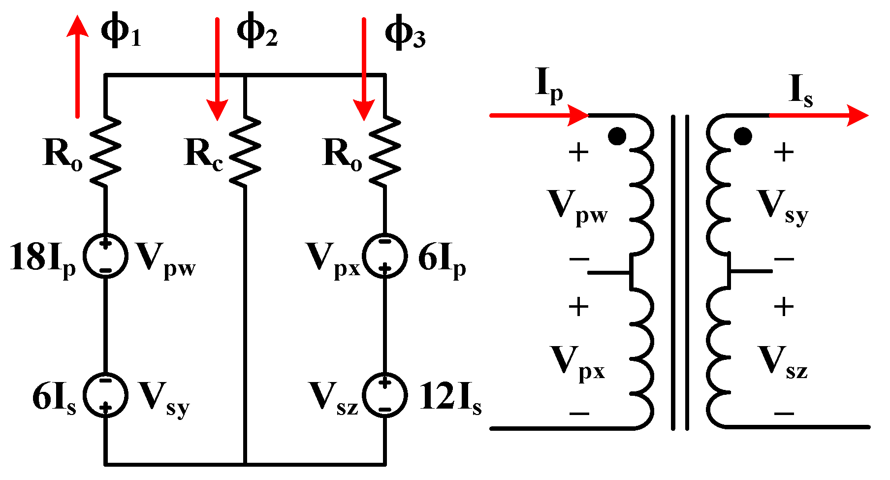
The conventional integrated leakage inductance is formed by leakage flux that is lost to the air and does not pass through the secondary side. Accurate control of the amount of leakage inductance is practically difficult. The concept of adjustable leakage inductance that was adopted in this study was to add an additional reluctance length that prevents some flux generated on the primary side from flowing into the secondary-side winding, in turn generating leakage inductance. The leakage inductance used in this study was designed using the concept of split flow of the transformer reluctance.
Figure 5 presents the concept of adjustable leakage inductance, where the voltage of the primary side and secondary side are denoted by
Vp and
Vs, respectively. The winding in the primary side was divided into two parts, of which one part wound counterclockwise with 18 turns around the left outer leg, and the other wound clockwise with 6 turns around the right outer leg. Similarly, the winding on the secondary side was also divided into two parts, in which one part wound clockwise with 6 turns around the left outer leg, and the other wound counterclockwise with 12 turns around the right outer leg. Moreover, according to Equation (6), the magnetomotive force (MMF) of these windings could be represented as 18
Ip, 6
Is, 6
Ip, and 12
Is, and their voltage as
Vpw,
Vpx,
Vsy, and
Vsz, respectively.
Ro represents the reluctance of the outer leg, and
Rc represents the reluctance of the center leg.
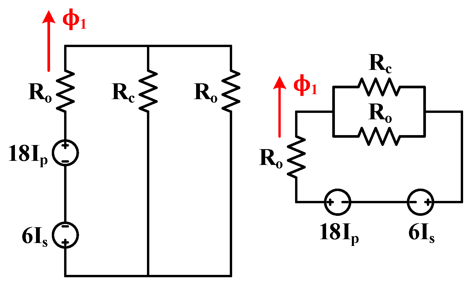
Figure 6 displays the equivalence of the reluctance generated by the passing flux produced in the left leg that was achieved by using the superposition theorem. Regarding the core structure, because the reluctances of both outer legs are the same, the equivalent reluctance passing through
ϕ1 and
ϕ3 are the same, as indicated in Equation (7). After the reluctance passing through the flux has been obtained,
ϕ1 could be presented as Equation (8); although the equivalent reluctance
of ϕ1 and
ϕ3 are the same,
ϕ3 could be presented as in Equation (9) because the MMF is different for each leg. Because the center leg had no windings, only the values of flux on the left and right outer legs are listed.
As mentioned, the MMF generated from the windings on each leg was determined using the superposition theorem. Subsequently, Equations (10)–(12) represent the total flux of each leg in consideration of flux split flow.
According to
Figure 7, the primary-side voltage of the transformer
Vp is the sum of
Vpw and
Vpx; the secondary-side voltage of the transformer
Vs is the sum of
Vsy and
Vsz. As demonstrated by Equation (13), Faraday’s law of induction was employed to ascertain the relationship between the voltage, number of turns, and variation in flux over time. Moreover, the primary-side voltage
Vp and secondary-side voltage
Vs of the transformer are represented using Equations (14) and (15).
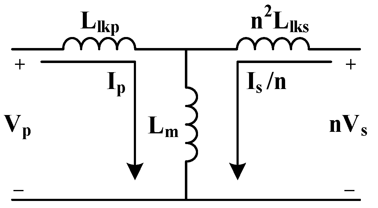
By using Faraday’s law of induction to assess the relationship between the voltage, reluctance, and number of turns of the transformer, the T model of the transformer (
Figure 7) could be applied. In
Figure 7,
Vp refers to the primary-side voltage of the transformer, and
Vs refers to the secondary-side voltage of the transformer; furthermore,
Llkp represents the primary-side leakage inductance,
Llks represents the secondary-side leakage inductance, and
Lm represents the excitation inductance of the transformer. The T model enabled the equivalence of the voltage, current, and leakage inductance of the secondary side with that of the primary side. Equations (16) and (17) present the results.
Subsequently, Equations (14) and (16) could be compared with Equations (15) and (17). Equations (18)–(20) represent the relationship among the leakage inductance and excitation inductance of the primary and secondary sides of the transformer and the number of turns of the windings.
The comparison could be used to establish models of equivalent leakage inductance of the primary and secondary sides of the transformer and the excitation inductance. Such models could be presented using Equations (21)–(23).
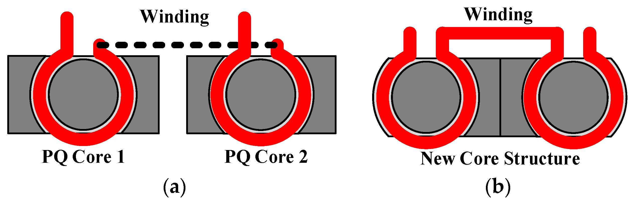
According to the obtained results, a three-legged core could achieve adjustable leakage inductance if the shape of the outer legs easily enables winding. Applying the winding coil is difficult when the commonly used PQ and RM cores are employed because of their outer leg shape; thus, EI or EE cores were used for adjustable leakage inductance [
21]. The simulation results of the current distribution of the PCB trace windings based on the shapes of the PQ and EI cores were obtained with Maxwell magnetic simulation software. The simulation results presented in
Figure 8 yielded the winding for the square core, and the current distribution obtained using the square core was considerably more uneven than that obtained using the round core, leading to excessively dense current at the corner of the winding, hot spots, and higher losses. Therefore, the cylindrical core was selected as the transformer core in this study.
The design presented in
Figure 9 was proposed to achieve adjustable inductance through winding on the two outer legs of the three-legged core and the obtainment of even current distributions on PCB windings. Producing adjustable leakage inductance required that windings be set only on the outer legs and not on the center leg. This method enabled the cross-sectional area of the center leg to be altered to a shape suitable for PCB winding, increasing the effectiveness of the winding space of the transformer. Therefore, this study proposed aligning two PQ cores (
Figure 9a), where the connected part serves as the center leg of the core, and removal of one outer leg of the original core forms a new three-legged structure for the core. The design is as presented in
Figure 9b.
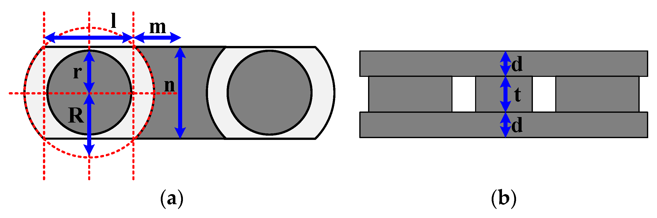
Figure 10 shows a diagram of the core size design in this study.
Figure 10a is the top view, and
r represents the radius of the effective cross-sectional area,
R denotes the radius of the core that can be wound,
l is twice the horizontal distance from the core cylinder to the highest point of the center leg,
m is the maximum width of the center leg,
n is the length of the core,
d is the thickness of the top and bottom pieces, and
t represents the leg height of the core.
The overall loss of the transformer can be divided into core loss and copper loss. Core loss is the product of core loss per unit volume and core volume, as shown in Equation (24). In Equation (25), Pv denotes the unit volume loss, and Cm, x, and y can be acquired from the core manufacturer’s manual. Combining Equations (24) and (25) reveals that the core loss and volume Vel are related to the switching frequency fs and peak flux density Bmax, with core loss being linearly proportional to Vel and exponentially proportional to fs and Bmax. Next, Bmax was expressed as Equation (26), where Vin denotes the input voltage, Ae represents the effective cross-sectional area of the core, and Np is the number of turns of the primary winding. In this study, the input voltage Vin, switching frequency fs, and effective cross-sectional area of the core are 400 V, 500 kHz, and 194 mm2, respectively. The relationship between core loss and the number of primary-side turns is revealed through Equation (26), with a higher number of turns leading to a drop in peak flux density, reducing the core loss. However, from the perspective of copper loss, more turns resulted in greater loss. Thus, the optimal number of turns in this study was acquired by quantifying the core loss and copper loss.
In this study, a full-bridge LLC resonant conversion topology was employed for the primary-side circuit architecture, whereas the secondary-side rectification architecture consisted of a full-bridge topology. The turns ratio of the transformer was calculated using Equation (27), and substituting the circuit specifications of this study (400 V input voltage and 300 V output voltage) yielded a transformer turns ratio of 4:3. However, the minimal number of turns on the primary side cannot be 1 because of the winding method of the adjustable leakage inductance, because the primary-side should be wound to the two outer legs, and because the primary side on both legs cannot be the same. Additionally, the winding ratio of the primary and secondary sides has to be an integer to prevent the need for a non-integer number of turns on the secondary side.
Table 4 shows that the winding width of the core could be obtained by subtracting
r from
R, and the actual winding width was 5.5 mm.
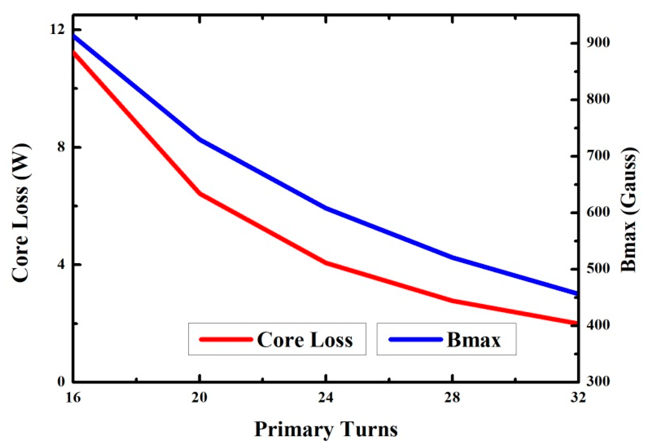
The transformer turns ratio in this study was 4:3; thus, the number of turns at the primary and secondary sides could be 4:3, 8:6, 12:9, and so on. The core loss per unit volume (Pv) increased substantially when the peak flux density of the transformer exceeded 1000 G. Therefore, the peak flux density was designed to be less than 1000 G in the core turns design. Next, Equation (26) was rewritten as Equation (28), and Bmax was set to 1000 G. According to Equation (28), the minimum number of winds on the primary side was 14.6. Practically, more windings mean more layers and greater costs. Therefore, only the following five windings on the primary and secondary sides were considered: 16:12, 20:15, 24:18, 28:21, and 32:24.
The peak flux density and core loss for different numbers of turns were obtained using Equations (24) and (26), and the results are plotted in
Figure 11. The relationship between core loss and number of turns was nonlinear. The difference in core loss between 16 and 20 turns on the primary-side winding was 4.8 W, whereas 28 and 32 turns on the primary-side winding yielded a core loss of approximately 0.8 W. This was the main reason for designing
Bmax to be less than 1000 G.
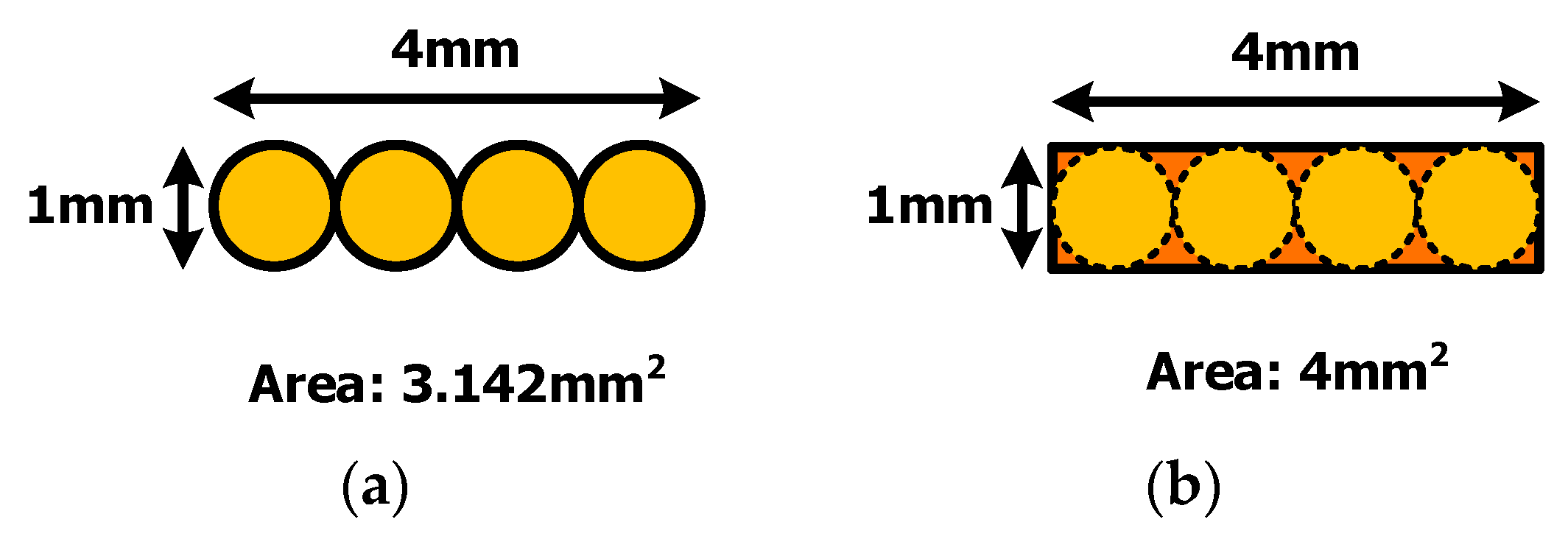
The high-frequency copper loss was analyzed next. Conventional transformers are mostly wound with litz wire; however, planar routing is more advantageous to utilize the window area of a transformer.
Figure 12 compares the use of planar routing and four litz wires. Under the same condition of an occupied area of 4 mm
2, the cross-sectional area of the litz wires was 3.142 mm
2, whereas that of the planar routing was 4 mm
2 (
Figure 12a,b, respectively); both yielded a 27% difference in DC resistance under the same length. Therefore, PCB routing was used as the transformer winding in this study to achieve high power density.
PCB routing was selected over litz wire under the same transformer window area because it resulted in lower DC resistance of the winding. However, a sharp rise in AC resistance loss was observed when the switching frequency was increased from the conventional 50 kHz–200 kHz to 500 kHz–1 MHz. Therefore, the AC resistance loss of the transformer winding was analyzed.
According to Dowell’s equation, the skin effect and proximity effect can be expressed by Equations (29) and (30), respectively, where
ξ =
h/
δ, with
h denoting the thickness of the copper wire in the transformer winding and
δ representing the skin depth of the transformer winding. Additionally,
m can be expressed using Equation (31), where
e represents the number of winding layers. The five numbers of windings that were employed and the corresponding distributions of MMF are displayed in
Figure 13. Because the circuit architecture in this study was an LLC rather than bidirectional CLLC, only the leakage inductance on the primary side was adjusted. Therefore, the secondary side was wound around the two outer legs with the same or almost the same number of turns, and the primary and secondary sides were wound on an eight-layer PCB in an interleaved manner. A total of seven layers of PCB winding were used, and one layer was reserved as the routing that connected the two leg windings.
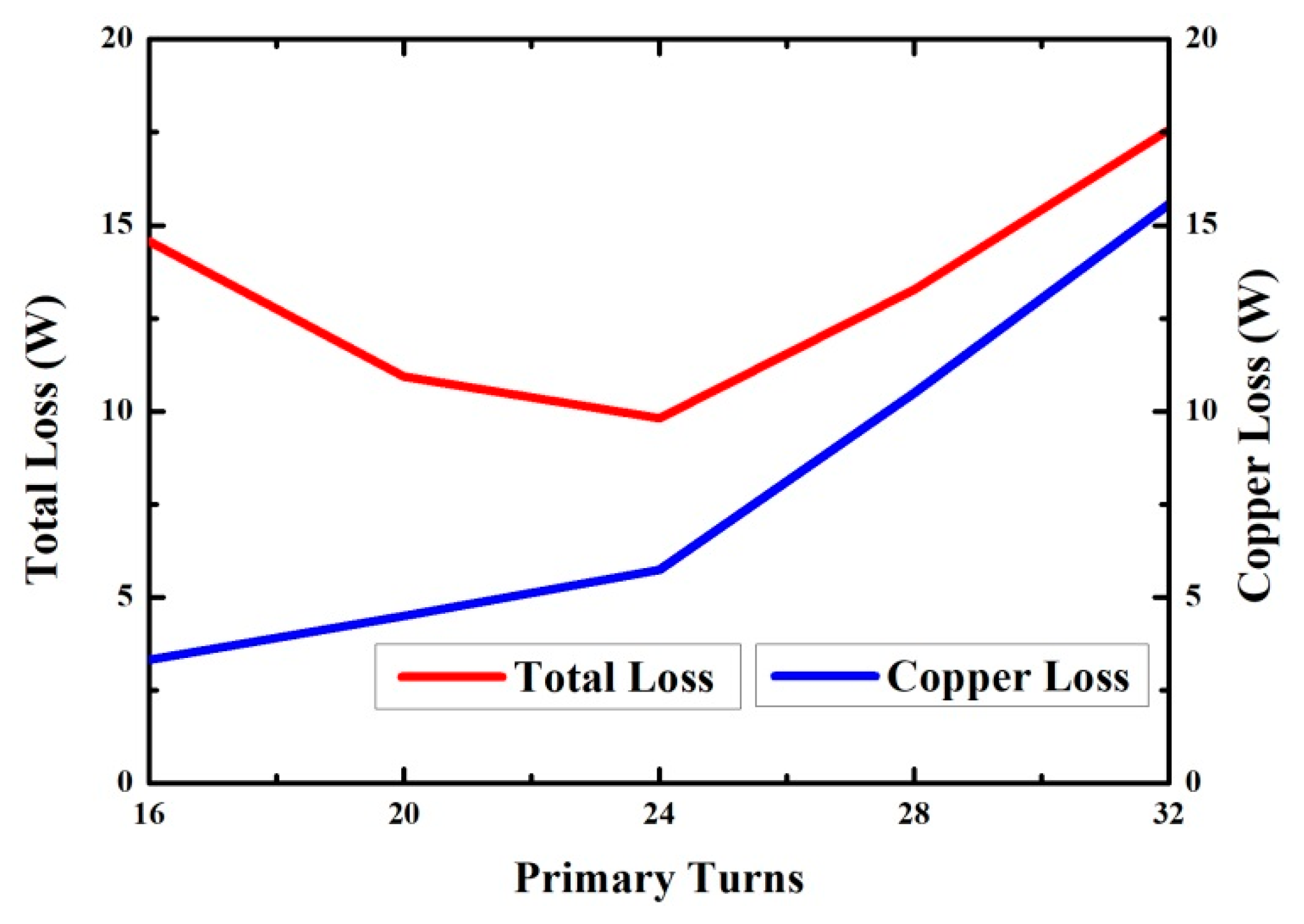
Figure 14 illustrates the copper loss and total loss of the transformer for different numbers of turns. The core loss could be obtained from
Figure 11. More turns resulted in lower peak flux density of the core and thus lower core loss. However, more windings also led to greater copper loss, which could be divided into that associated with DC resistance and AC resistance. DC resistance was greater for more windings; however, the resistance that actually affects the high-frequency copper loss is AC resistance loss. Because an eight-layer board was used for transformer routing, more turns meant that each layer of the PCB board had to accommodate more windings, which narrowed the width of each winding. Moreover, according to
Figure 13, more windings in each layer resulted in a higher MMF, causing substantially greater AC resistance under high frequency, which in turn resulted in greater copper loss. The various amounts of core loss and copper loss are presented in
Table 5, and the results are plotted in
Figure 14. Ultimately, the number of turns with the lowest total loss (24:18) was selected as the suitable number of turns of the transformer in this study.
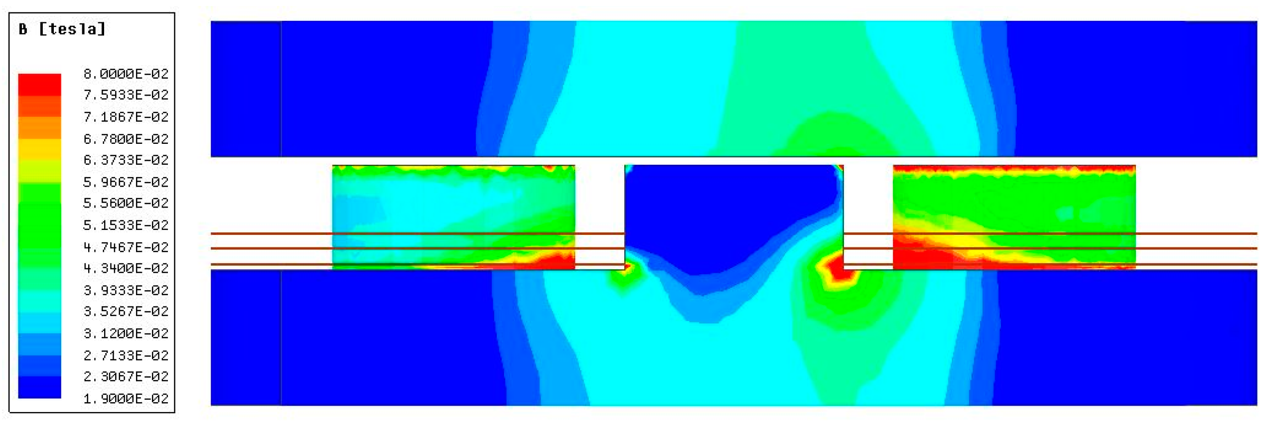
Figure 15 shows the peak flux density of the core, as simulated by ANSYS Maxwell software, to verify that the core operated normally.


