Article

Extension of Zero Voltage Switching Capability for CLLC Resonant Converter

1
Ulsan National Institute of Science and Technology (UNIST), Ulsan KS017, Korea
2
LIG Nex1, Seongnam KS009, Korea
*
Author to whom correspondence should be addressed.
Energies 2019, 12(5), 818; https://doi.org/10.3390/en12050818
Submission received: 18 January 2019 / Revised: 26 February 2019 / Accepted: 27 February 2019 / Published: 1 March 2019
(This article belongs to the Special Issue Advances in High-Efficiency LLC Resonant Converters)

Abstract

:
TheCLLC resonant converter has been widely used to obtaina high power conversion efficiency with sinusoidal current waveforms and a soft switching capability. However, it has a limited voltage gain range according to the input voltage variation. The current-fed structure canbe one solution to extend the voltage gain range for the wide input voltage variation, butit has a limited zero voltage switching (ZVS) range. In this paper, the current-fed CLLC resonant converter with additional inductance is proposed to extend the ZVS range. The operational principle is analyzed to design the additional inductance for obtaining the extended ZVS range. The design methodology of the additional inductance is proposed to maximize the ZVS capability for the entire load range. The performance of the proposed method is verified with a 20 W prototype converter.

1. Introduction

Recently, the small sized power converterhas become significant in various industries, such as lightings, TVs, computers, and other home appliances [1,2]. A power converter operating at a high switching frequency is one effective method to improve power density [3,4,5,6,7]. However, the high switching frequency operation induces a large switching loss for the turn-on and turn-off states. Therefore, a soft switching capability is important to obtain a high power conversion efficiency in a high switching frequency operation [8,9,10]. Resonant power converters, such as LC resonance, LLC resonance, CLLC resonance, and CLL resonance, can implement the soft switching capability by the resonance, which can be a good candidate to implement the high switching frequency operation [11,12,13,14,15]. In addition, the wide band-gap device (WBD), such as gallium nitride (GaN) and silicon carbide (SiC), can increase the switching frequency up to several MHz compared with conventional silicon (Si)-based switching devices [16,17,18,19].
The CLLC resonant converter operating at the inductive region can obtaina zero voltage switching (ZVS) capability [20,21,22,23]. However, the large input voltage variation by the batteryinduces large switching frequency variation. In addition, the voltage gain fluctuation makes a non-ZVS operation withthe capacitive operation of the converter [24]. Therefore, the CLLC resonant converter has poor voltage gain characteristics according to the wide input voltage variation. The current-fed CLLC resonant converter can overcome the input voltage variation by the battery, since the current-fed structure compensates the input voltage variation [25,26]. However, the current-fed structure makes a limited ZVS capability of the low side switch, since the low side switch operates as the boost converter and resonant converter simultaneously. Therefore, the increase of the ZVS capability is significant to obtain a high power conversion efficiency for the entire load condition.
In this paper, the current-fed CLLC resonant converter employing the additional inductance is proposed to improve the ZVS capability. The operational principle of the proposed additional inductance is analyzed with the theoretical waveforms. From the operational principle, the design methodology of the additional inductance is analyzed to obtain the ZVS capability for the entire input voltage range and load conditions. The experimental results with a 20 W prototype converter verify the validity of the proposed additional inductance.

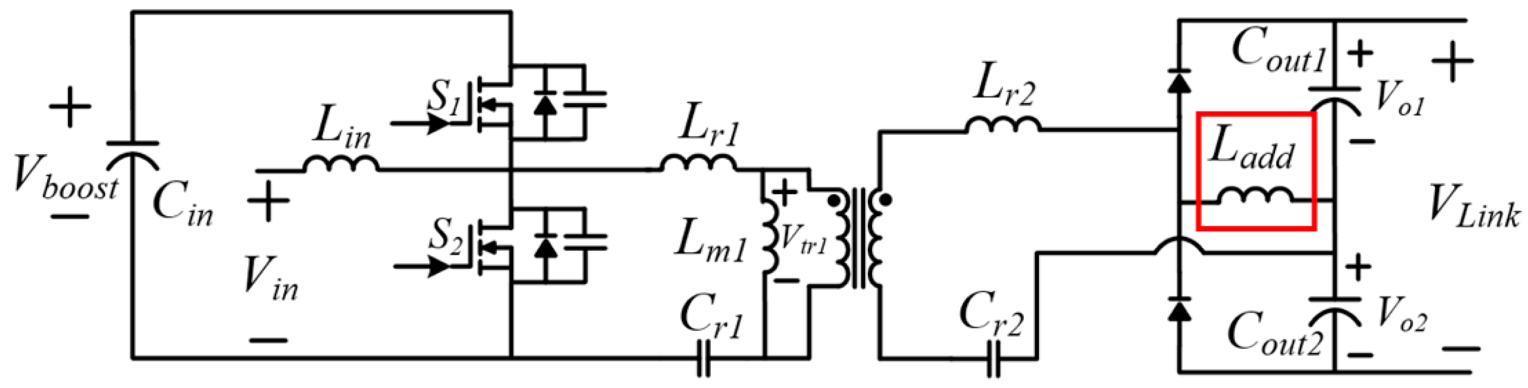
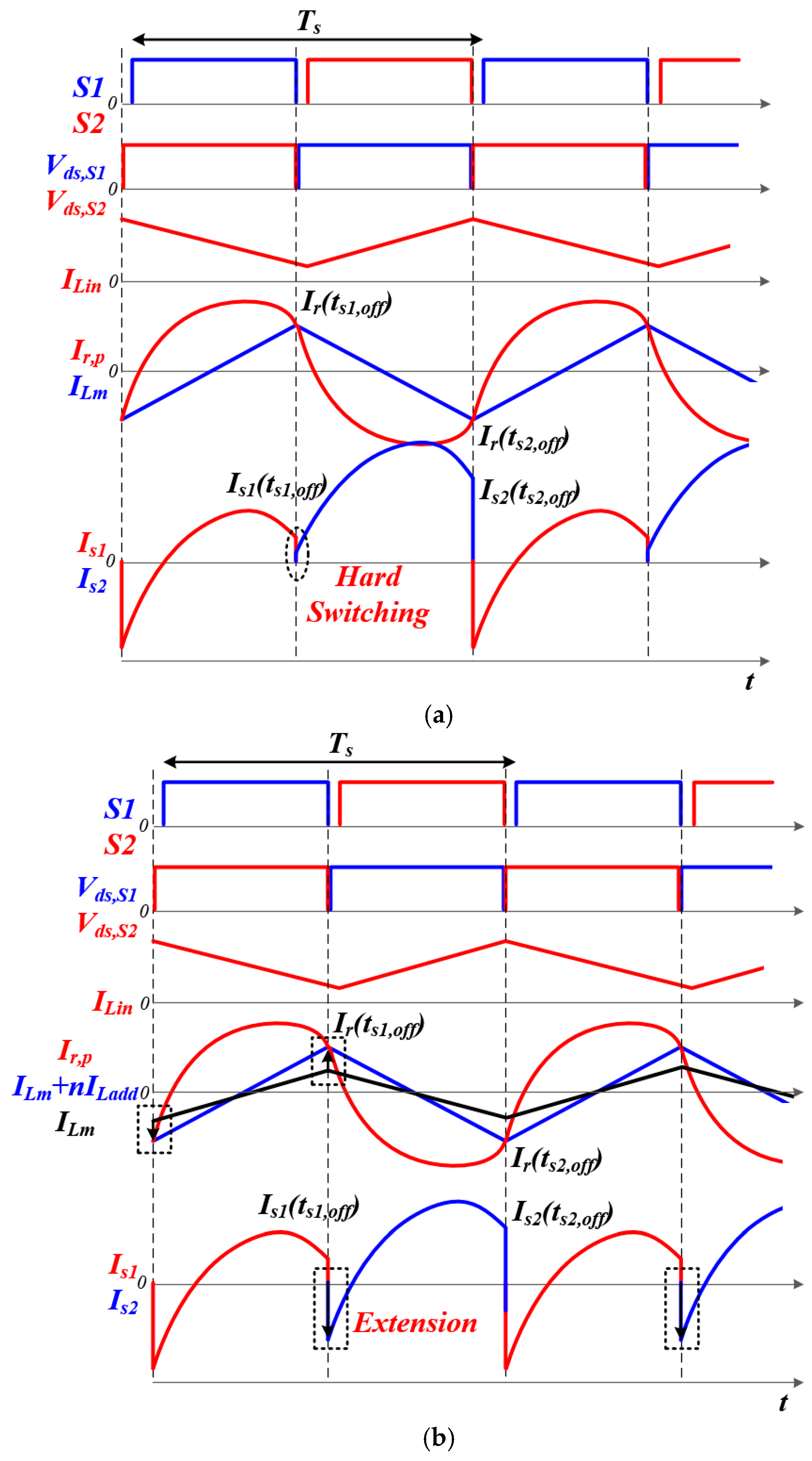
2. Operational Principle

Figure 1 shows the scheme of the proposed current-fed CLLC resonant converter. The current-fed structure regulates the wide input voltage variation with the asymmetric pulse width modulation (APWM), because it operates as the synchronous boost converter. The CLLC resonant tank provides the galvanic isolation using the transformer and resonance. The voltage doubler structure of the secondary side can reduce the turn ratio of the transformer.
Figure 2 shows the operational waveform of the conventional and the proposed current-fed CLLC resonant converter where S1and S2 are the primary switches, Vds,S1 and Vds,S2 is the drain-source voltage of S1 and S2, respectively, ILin is the current passing through the input inductor, Ir,p is the resonant current in the primary side, ILm is the magnetizing current, IS1 and IS2 are the currents passing through S1 and S2, respectively, and ILadd is the current in the additional inductance. The current-fed structure operates as the conventional boost converter by the switching operation of S1 and S2. The CLLC resonant tank employing the APWM has zero offset current on the magnetizing inductance which reduces the core and conduction losses of the transformer.
The current-fed structure is proper to compensate the wide input voltage variation. However, it limits the ZVS range according to the increase of the output load. The switch current of conventional voltage-fed CLLC resonant converter for the ZVS capability can be derived as follows:
Z V S S 1 = I r ( t S 2 , o f f )
Z V S S 2 = I r ( t S 1 , o f f )
where Ir(ts2,off) and Ir(ts1,off) are the resonant current at the turn off state of power switches, respectively. The negative current of each switch is required to obtain the ZVS condition. In the voltage-fed CLLC resonant converter, the resonant current onlydetermines the ZVS condition of each switch. In the case of the current-fed CLLC resonant converter, the input inductor and resonant currents determine the ZVS current.The switch current of the current-fed CLLC resonant converter for the ZVS capability can be derived as follows:
Z V S S 1 , c = I r ( t S 2 , o f f ) I L i n ( t s 2 , o f f )
Z V S S 2 , c = I r ( t S 1 , o f f ) + I L i n ( t s 1 , o f f )
where ILin(ts2,off) and ILin(ts2,off) are the input inductor current at the turn off state of power switches, respectively. The high side switch (S1) has a larger ZVS condition compared with Equation (1). However, the low side switch (S2) has a poor ZVS condition compared with Equation (2). Figure 2a shows the theoretical waveforms of the conventional current-fed CLLC resonant converter, whichhas a hard switching operation on the S2. The ZVS capability of the proposed CLLC resonant converter can be derived as follows:
Z V S S 1 , p = I r ( t S 2 , o f f ) I L i n ( t s 2 , o f f ) n I L a d d ( t s 2 , o f f )
Z V S S 2 , p = I r ( t S 1 , o f f ) + I L i n ( t s 1 , o f f ) n I L a d d ( t s 1 , o f f )
where ILadd(ts2,off) and ILadd(ts2,off) are the additional inductor currents at the turn off state of power switches, respectively, and n is the transformer turn ratio. Figure 2b shows the theoretical waveforms of the proposed CLLC resonant converter. The additional inductance extends the ZVS range compared with the conventional current-fed CLLC resonant converter.
The turnon current for the ZVS condition of the current-fed CLLC resonant converter can be calculated with the input inductor current and resonant current. The ZVS condition on the low side switch can be derived as follows:
I z v s , s 2 = 1 1 D s 2 V b o o s t R + ( V i n V b o o s t ) 2 L ( 1 D s 2 ) T s V t r 1 L m 1 D s 2 2 T s
where Ds2is the duty ratio of S2, Vboost is the voltage of the current-fed structure, Vin is the input voltage of the battery, R is the load resistance, L is the input inductance, Ts is the switching time, Lm is the magnetizing inductance, and Vtr1 is the transformer voltage. The negative value of Izvs,S2 guarantees the ZVS capability of S2.The decrease of the load resistance makes no ZVS condition of S2. In addition, the large duty ratio of S2 makes the worst ZVS condition, which means that the low input voltage condition is the worst ZVS condition.
The turn on current for ZVS condition of the low side switch with the proposed converter can be derived as follows:
I z v s , s 2 , p = 1 1 D s 2 V b o o s t R + ( V i n V b o o s t ) 2 L ( 1 D s 2 ) T s V t r 1 L m 1 D s 2 2 T s V o 1 n L a d d 1 D s 2 2 T s
where Vo1is the voltage on the output capacitor as shown in Figure 1. The proposed converter extends the ZVS condition with the additional inductor on the secondary side as shown in Figure 2b. Figure 3 shows the ZVS capability according to the additional inductance. The ZVS current is the turn on current of S2, which is required to have a negative value in order to obtain the ZVS capability. The small additional inductance is proper to extend the ZVS range. However, the small additional inductance increases the conduction loss on the primary side.Therefore, the design methodology of the additional inductanceis required to obtain the ZVS capability for the entire load range.
The voltage gain according to the duty ratio can be described in Figure 4. The proposed converter has similar voltage gain to that of the conventional boost converter, which shows wide duty ratio variations to regulate the output voltage. The additional inductance can be designed at the worst duty ratio case, which is the maximum duty ratio of S2.

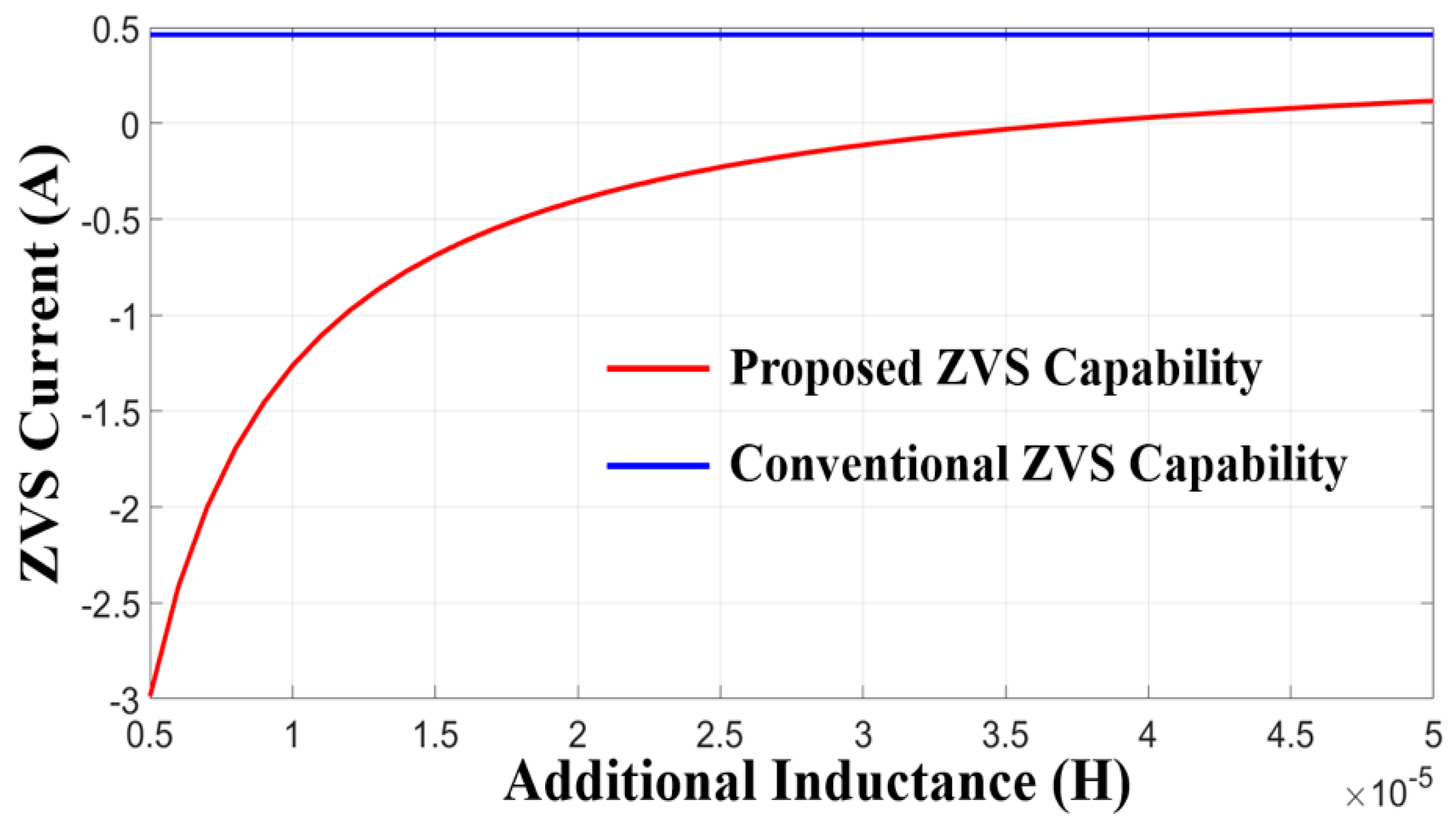
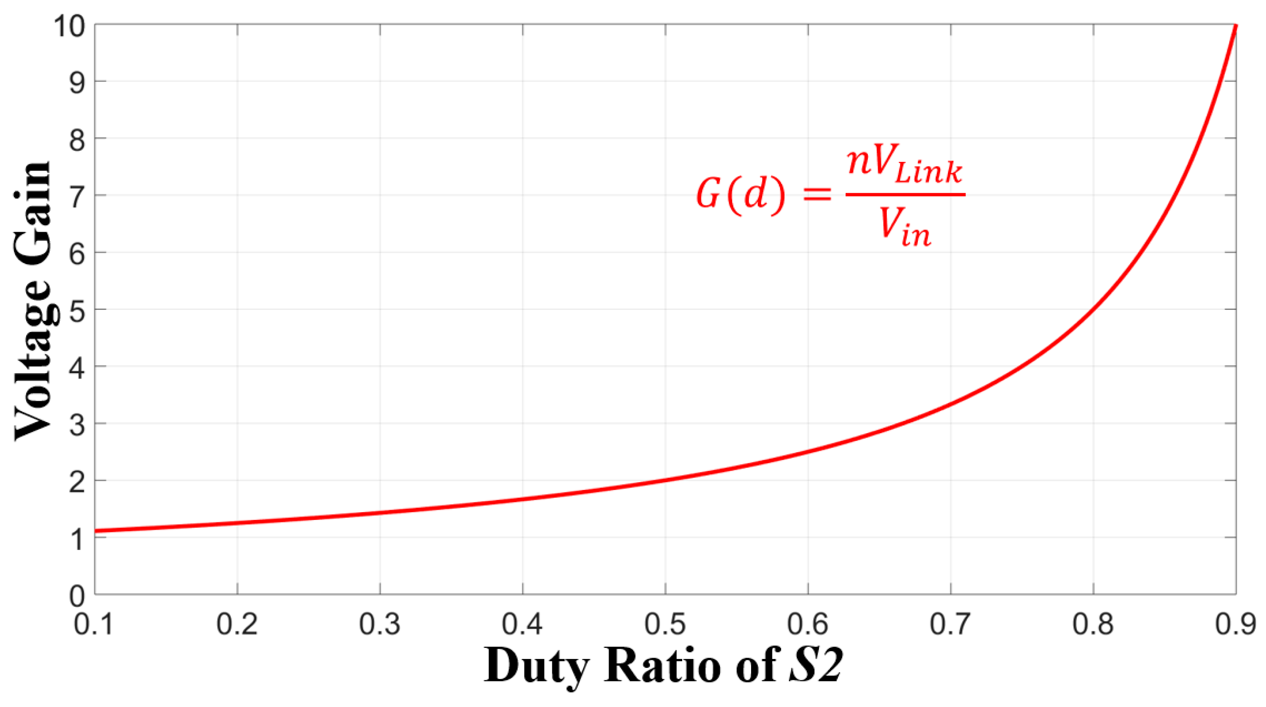
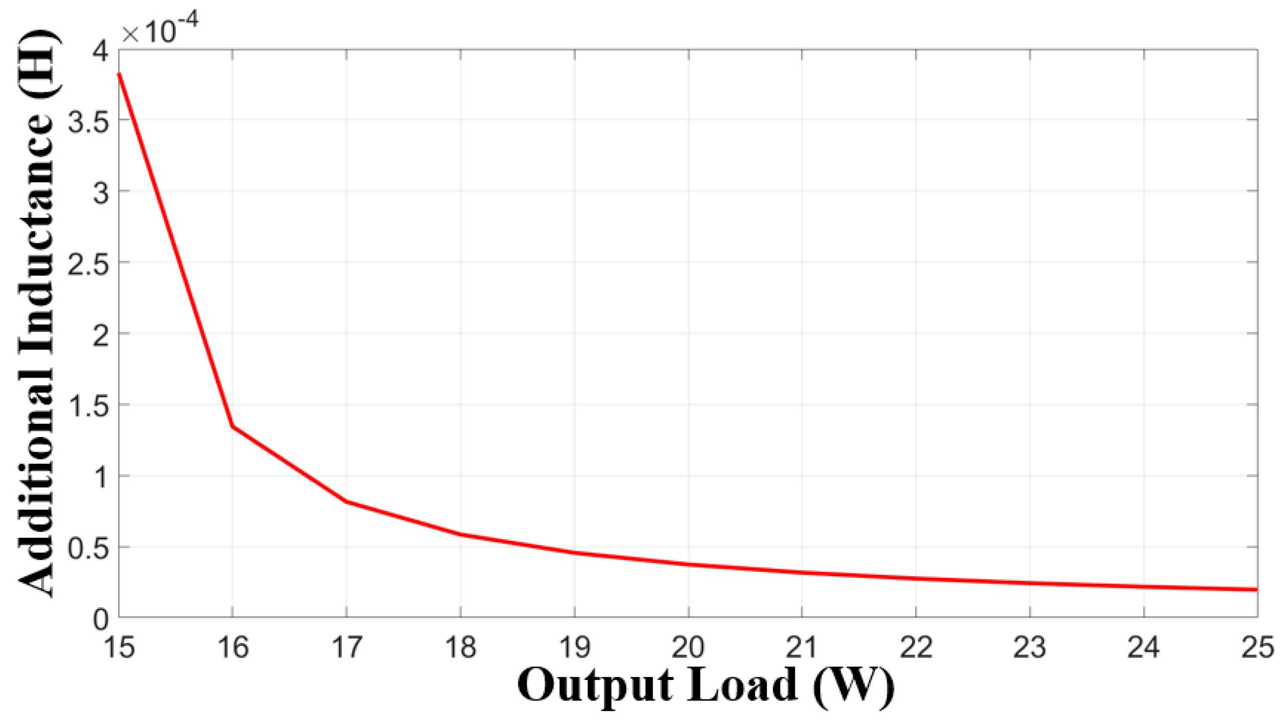
3. Design Methodology of Additional Inductance

The small additional inductance induces the conduction loss with large circulating current. The large additional inductance cannot obtain the ZVS capability of primary switches. Therefore, the maximum additional inductance is required to obtain the ZVS capability and the minimum conduction loss on the additional inductance, which can be derived with Equation (8) as follows:
L a d d = V o 1 n A 1 D s 2 2 T s A = 1 1 D s 2 V b o o s t R + ( V i n V b o o s t ) 2 L ( 1 D s 2 ) T s V t r 1 L m 1 D s 2 2 T s
The proper additional inductance can be designed from Equation (9). Figure 5 shows the additional inductance according to the output load condition. The increment of output load requires smaller additional inductance. The design specification is shown in Table 1. The input voltage has a large variation by the state of charge (SOC) of the battery. The load voltage is fixed, and rated load is 20 W. The resonant frequency(fr) is 200 kHz. The APWM requires the small resonant inductance to obtain the linear voltage gain according to the duty variation.The turn ratio is determined with the input voltage and output voltage ratio. The additional inductance is determined by (9).

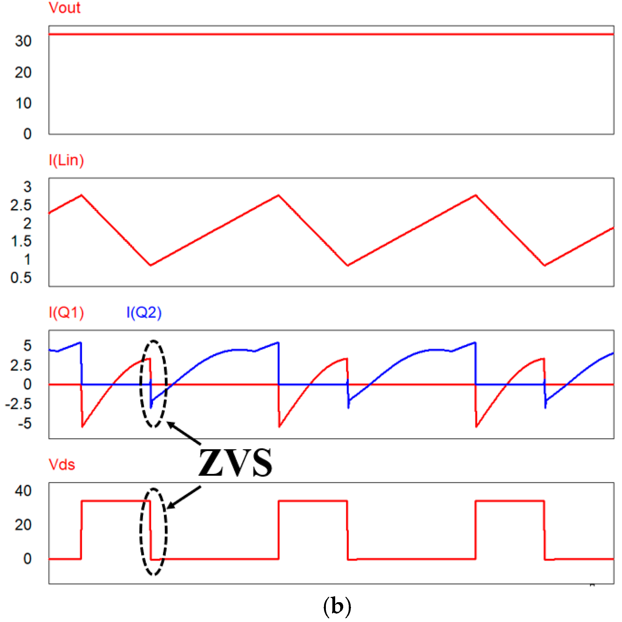
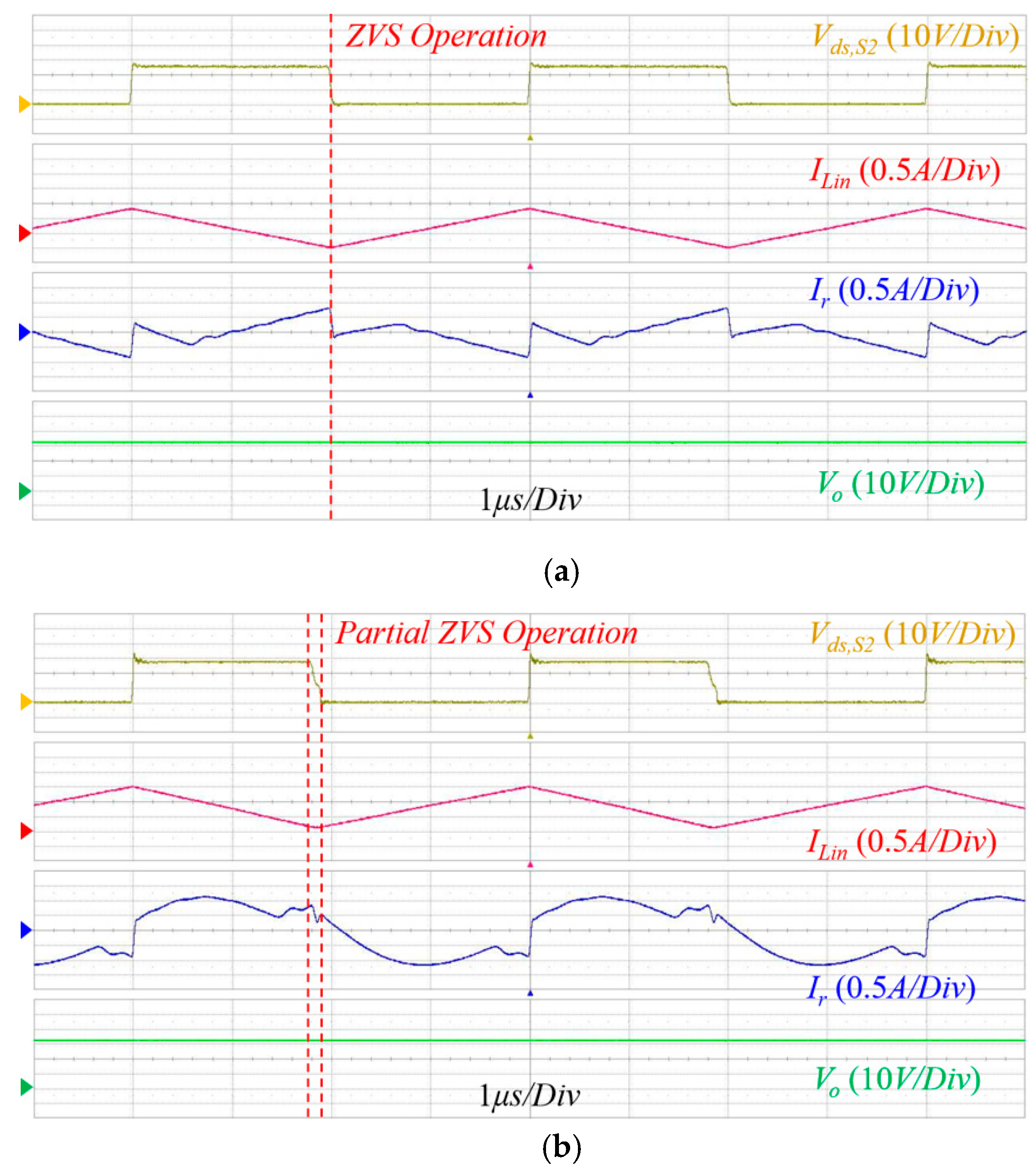
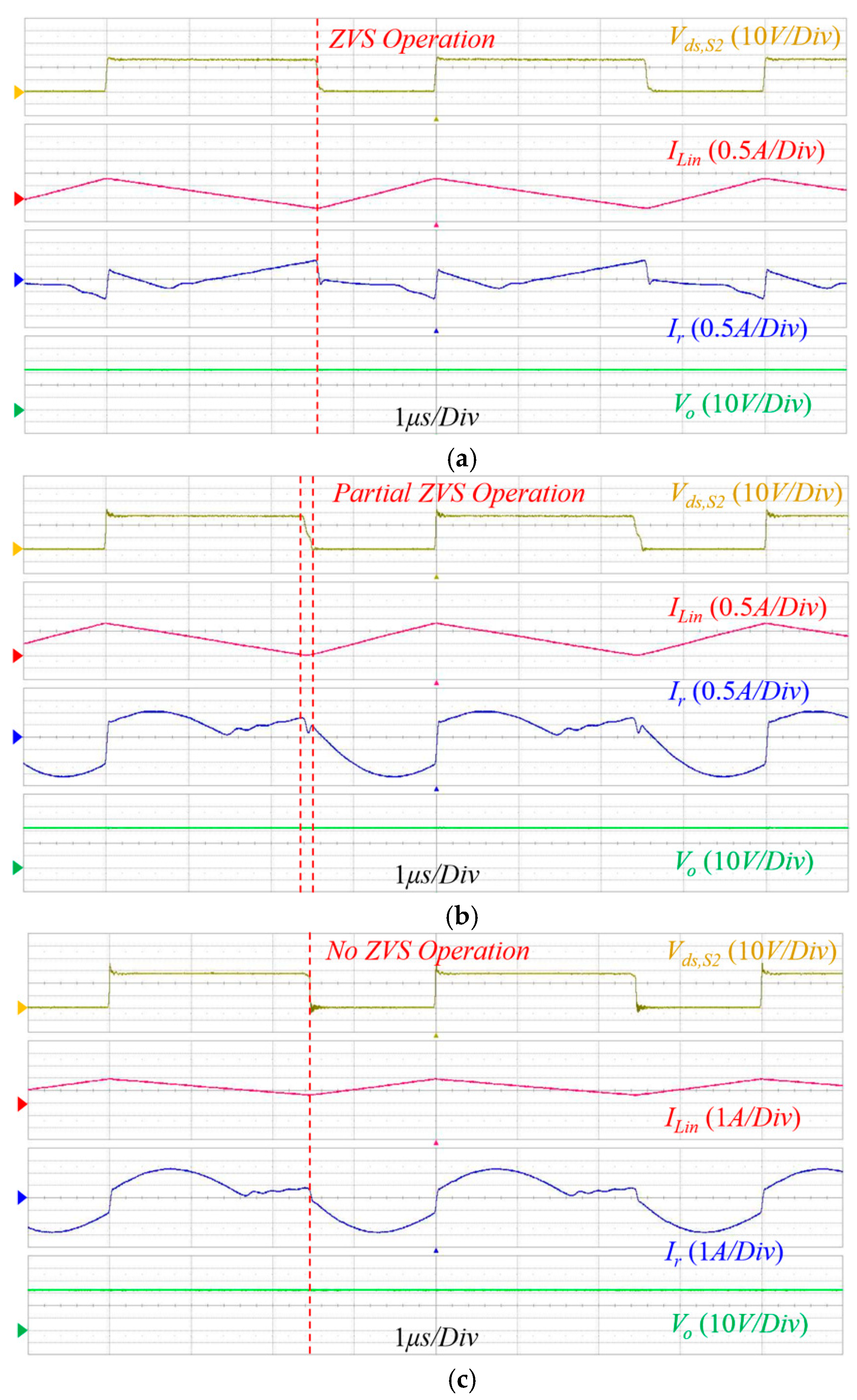
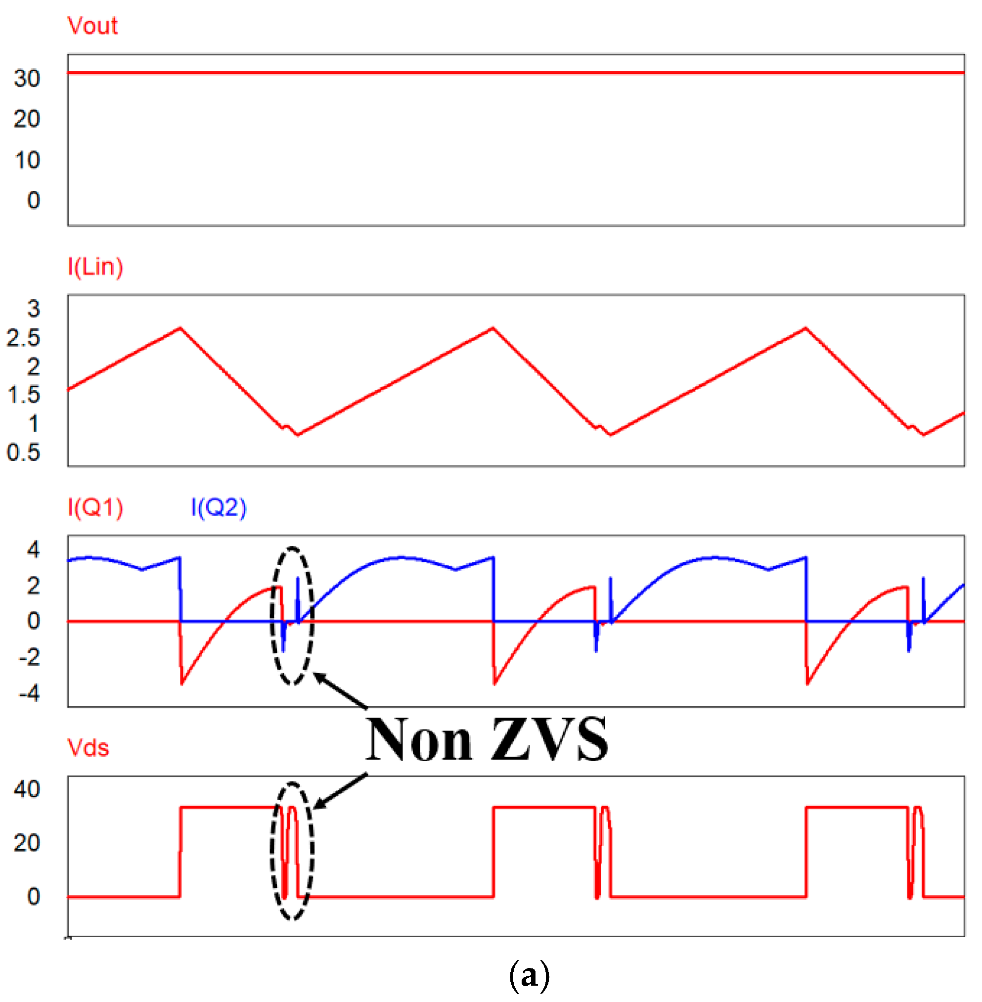
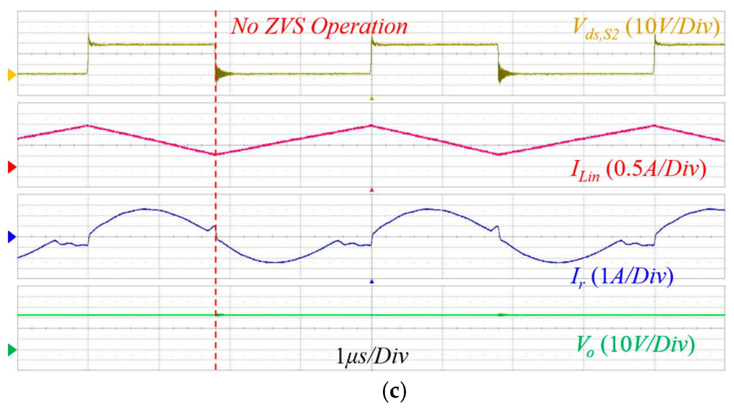
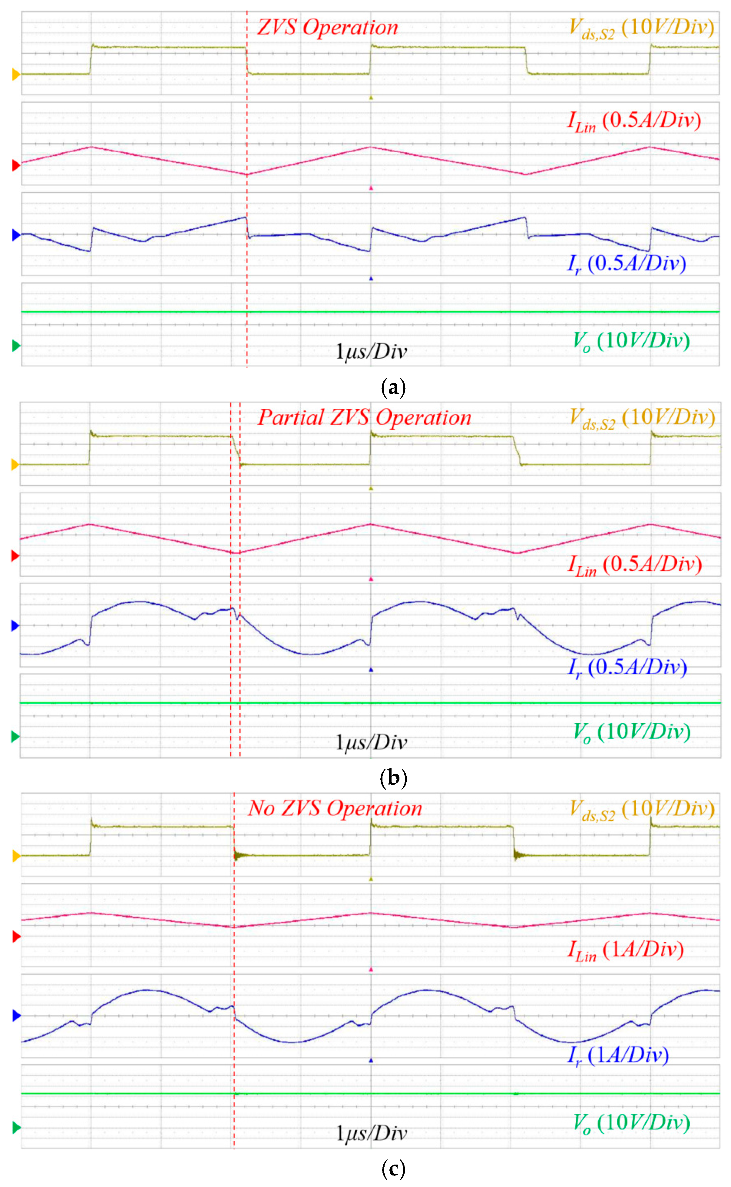
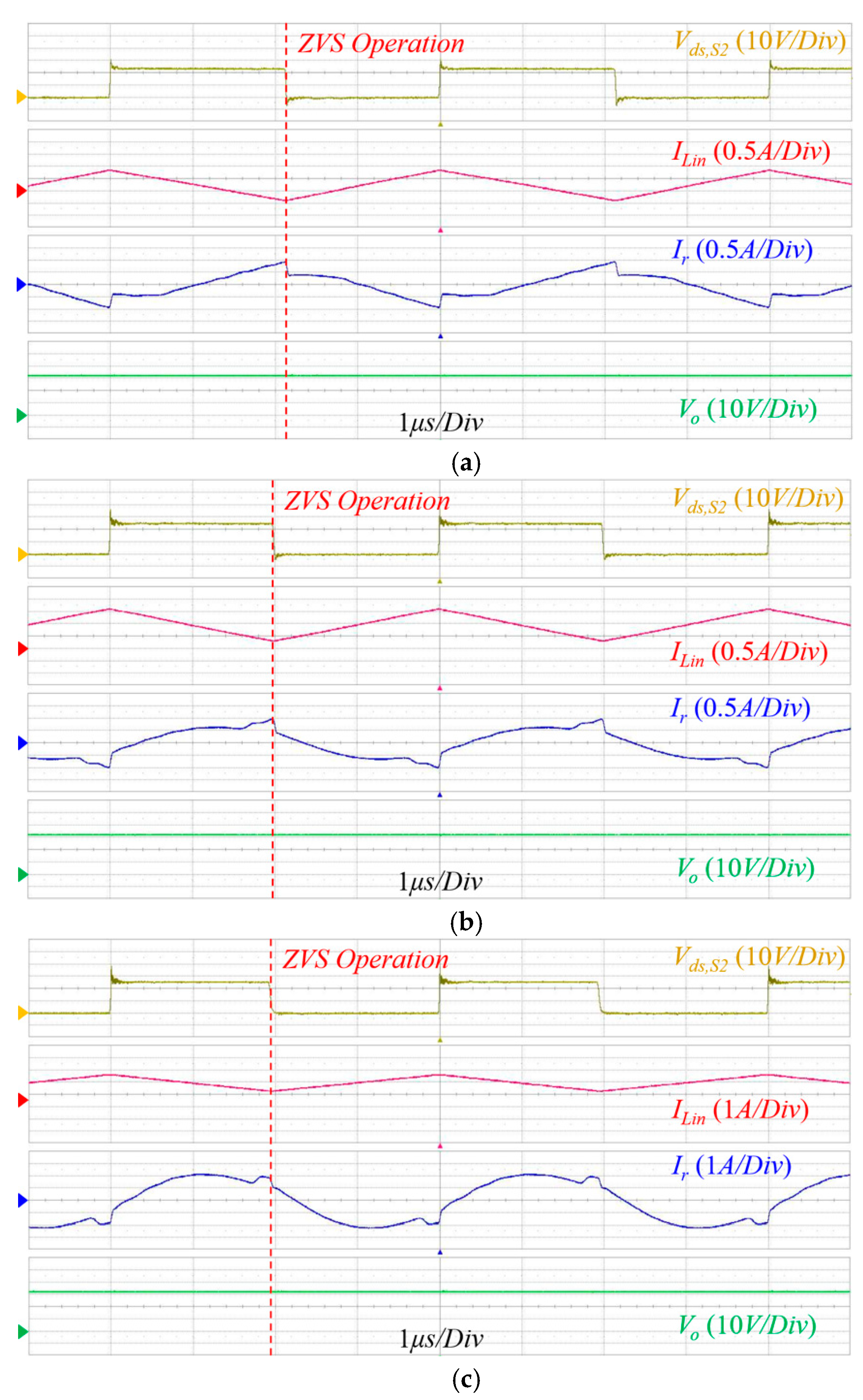
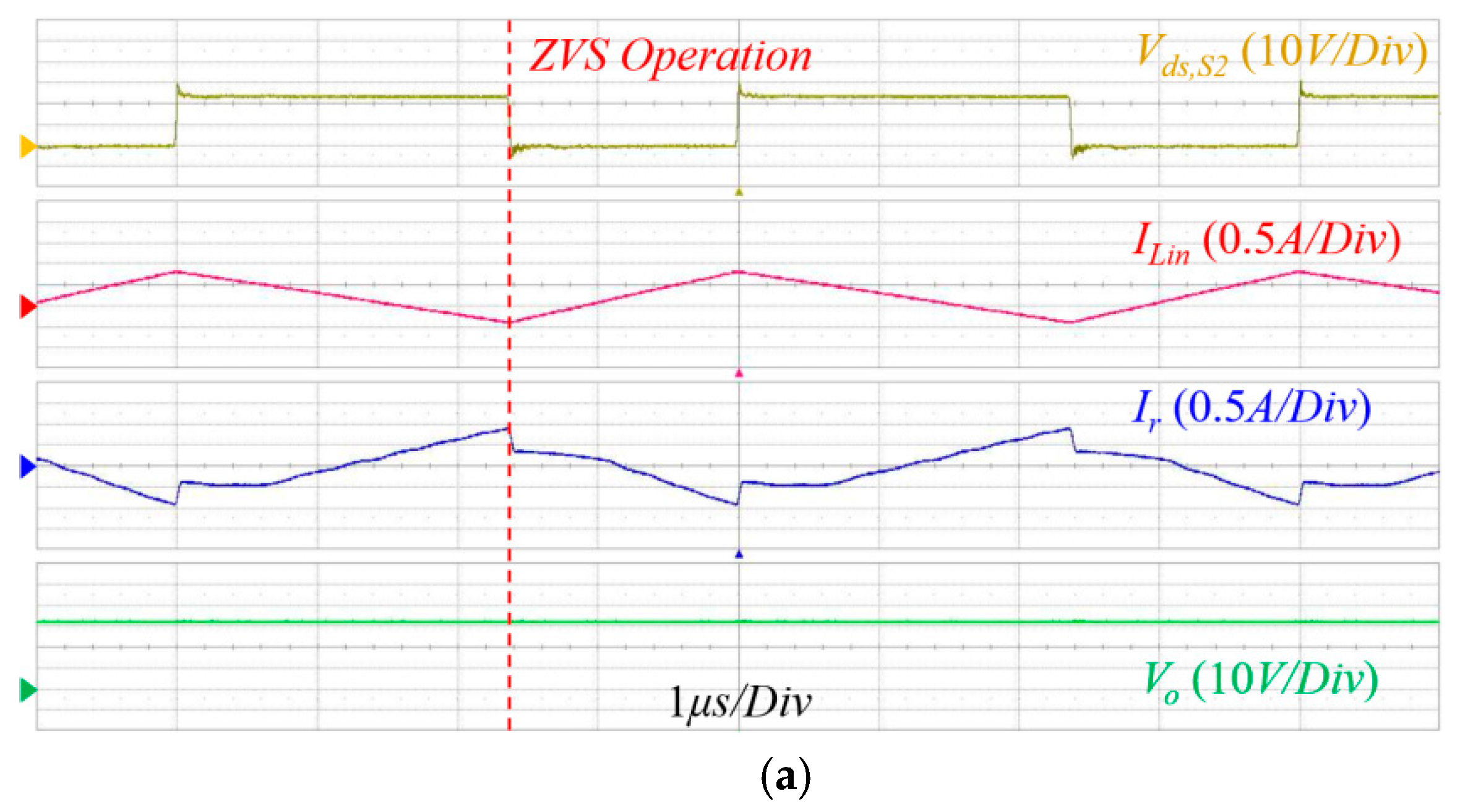
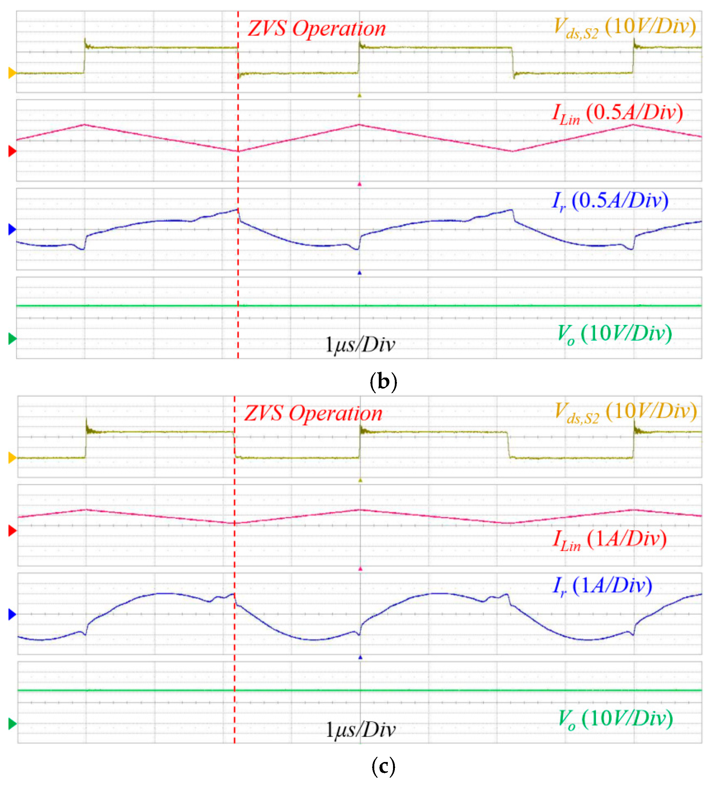
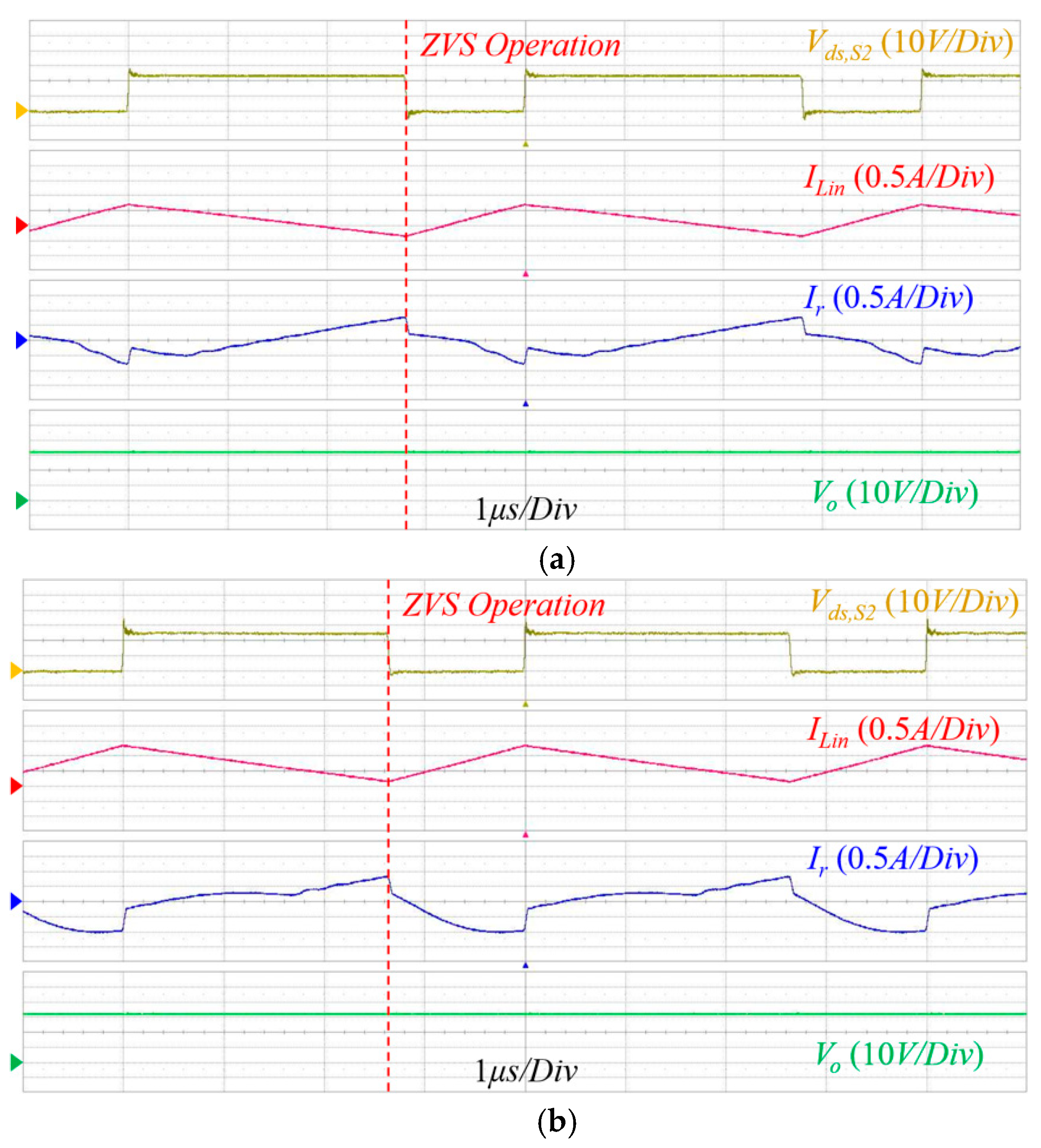
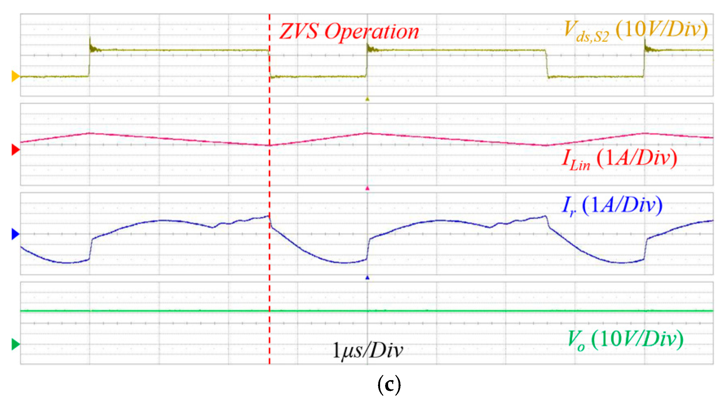
4. Simulation and Experimental Results

The simulation results show the ZVS capability according to the additional inductance, as shown in Figure 6. The conventional current-fed CLLC resonant converter has no ZVS capability on the bottom side switch. However, the proposed CLLC resonant converter employing the additional inductance can achieve the ZVS condition for both the power switches.
Figure 7, Figure 8 and Figure 9 show the steady state waveforms of the conventional CLLC resonant converter according to the input voltage variation and load condition. The duty ratio regulates the output voltage according to the load conditions and input voltages.At the light load condition, it shows the ZVS operation. However, the CLLC resonant converter has a partial and no ZVS operation for the middle load and full load conditions, respectively. For allthe input voltage range, the ZVS can be achieved at only the light load condition.
Figure 10, Figure 11 and Figure 12 show the steady state waveforms of the proposed CLLC resonant converter according to the input voltages and load conditions.The proposed converter shows the ZVS operation for the entire load and input voltage conditions.The extended soft switching capability improves the power conversion efficiency compared with the partial or no ZVS cases. The power loss of the partial and no ZVS cases can be calculated as follows:
P n o Z V S 1 2 V d s , c I o n t o n f s w
where PnoZVS is the power loss according to the partial or no ZVS conditions, Vds,c is the drain-source voltage at the turn on state, Ion is the switch current at the turn on state, ton is the turn on time duration, and fsw is the switching frequency. Figure 13 shows the comparison of the power conversion efficiency between the conventional current-fed CLLC resonant converter and the proposed converter. For the light load condition, the proposed and conventional methods can obtain ZVS capability at the light load condition, which makes no difference in terms of the efficiency. However, the proposed converter has a higher power conversion efficiency for the middle to full load conditions. The maximum improvement of power conversion efficiency is 1% at the middle load condition.

5. Conclusions

A soft switching capability can improve the power conversion efficiency of the power converter. In this paper, the current-fed CLLC resonant converter employing the additional inductance is proposed to extend the ZVS capability. The operational principle and the design methodology of the additional inductance are analyzed to obtain the soft switching capability for the entire load and input voltage conditions. The simulation and experimental results verify the soft switching performance of the proposed CLLC resonant converter compared with the conventional converter. The maximum efficiency improvement using the proposed converter is 1% at the middle load condition.

Author Contributions

Conceptualization, H.P., J.J.; Methodology, H.P.; Software, H.P.; Validation, H.P.; Resources, D.K., S.B., J.J.; Writing-Original Draft Preparation, H.P.; Writing-Review & Editing, J.J.; Supervision, D.K, J.J.; Project Administration, D.K., S.B.; Funding Acquisition, J.J.

Funding

This research is performed based on the cooperation with UNIST-LIG Nex1 Cooperation.

Conflicts of Interest

The authors declare no conflict of interest.

References

  1. De Doncker, R.W.; Divan, D.M.; Kheraluwala, M.H. A three-phase soft-switched high-power-density DC/DC converter for high-power applications. IEEE Trans. Ind. Appl. 1991, 27, 63–73. [Google Scholar] [CrossRef]
  2. Liu, Y.-C.; Chen, M.-C.; Yang, C.-Y.; Kim, K.A.; Chiu, H.-J. High-Efficiency Isolated Photovoltaic Microinverter Using Wide-Band Gap Switches for Standalone and Grid-Tied Applications. Energies 2018, 11, 569. [Google Scholar] [CrossRef]
  3. Zaman, H.; Wu, X.; Zheng, X.; Khan, S.; Ali, H. Suppression of Switching Crosstalk and Voltage Oscillations in a SiC MOSFET Based Half-Bridge Converter. Energies 2018, 11, 3111. [Google Scholar] [CrossRef]
  4. Pilawa-Podgurski, R.C.N.; Sagneri, A.D.; Rivas, J.M.; Anderson, D.I.; Perreault, D.J. Very-High-Frequency Resonant Boost Converters. IEEE Trans. Power Electron. 2009, 24, 1654–1665. [Google Scholar] [CrossRef]
  5. Reusch, D.; Strydom, J. Understanding the Effect of PCB Layout on Circuit Performance in a High-Frequency Gallium-Nitride-Based Point of Load Converter. IEEE Trans. Power Electron. 2014, 29, 2008–2015. [Google Scholar] [CrossRef]
  6. Kaiwei, Y.; Yang, Q.; Ming, X.; Lee, F.C. A novel winding-coupled buck converter for high-frequency, high-step-down DC-DC conversion. IEEE Trans. Power Electron. 2005, 20, 1017–1024. [Google Scholar]
  7. Meng, Z.; Wang, Y.-F.; Yang, L.; Li, W. High Frequency Dual-Buck Full-Bridge Inverter Utilizing a Dual-Core MCU and Parallel Algorithm for Renewable Energy Applications. Energies 2017, 10, 402. [Google Scholar] [CrossRef]
  8. Huang, R.; Mazumder, S.K. A Soft-Switching Scheme for an Isolated DC/DC Converter With Pulsating DC Output for a Three-Phase High-Frequency-Link PWM Converter. IEEE Trans. Power Electron. 2009, 24, 2276–2288. [Google Scholar] [CrossRef]
  9. Liu, X.; Liu, J.; Wang, J.; Wang, C.; Yuan, X. Design Method for the Coil-System and the Soft Switching Technology for High-Frequency and High-Efficiency Wireless Power Transfer Systems. Energies 2018, 11, 7. [Google Scholar] [CrossRef]
  10. Liu, K.H.; Lee, F.C. Zero-voltage switching technique in DC/DC converters. IEEE Trans. Power Electron. 1990, 5, 293–304. [Google Scholar] [CrossRef]
  11. Lin, B.-R.; Wu, G.-Y. Bidirectional Resonant Converter with Half-Bridge Circuits: Analysis, Design, and Implementation. Energies 2018, 11, 1259. [Google Scholar] [CrossRef]
  12. Lin, B.-R. Investigation of a Resonant dc–dc Converter for Light Rail Transportation Applications. Energies 2018, 11, 1078. [Google Scholar] [CrossRef]
  13. Zhang, S.-H.; Luo, F.-Z.; Wang, Y.-F.; Liu, J.-H.; He, Y.-P.; Dong, Y. Control Method Based on Demand Response Needs of Isolated Bus Regulation with Series-Resonant Converters for Residential Photovoltaic Systems. Energies 2017, 10, 752. [Google Scholar] [CrossRef]
  14. Lin, R.; Huang, L. Efficiency Improvement on LLC Resonant Converter Using Integrated LCLC Resonant Transformer. IEEE Trans. Ind. Appl. 2018, 54, 1756–1764. [Google Scholar] [CrossRef]
  15. Tan, X.; Ruan, X. Equivalence Relations of Resonant Tanks: A New Perspective for Selection and Design of Resonant Converters. IEEE Trans. Ind. Electron. 2016, 63, 2111–2123. [Google Scholar] [CrossRef]
  16. Fayyaz, A.; Romano, G.; Urresti, J.; Riccio, M.; Castellazzi, A.; Irace, A.; Wright, N. A Comprehensive Study on the Avalanche Breakdown Robustness of Silicon Carbide Power MOSFETs. Energies 2017, 10, 452. [Google Scholar] [CrossRef]
  17. Efthymiou, L.; Camuso, G.; Longobardi, G.; Chien, T.; Chen, M.; Udrea, F. On the Source of Oscillatory Behaviour during Switching of Power Enhancement Mode GaN HEMTs. Energies 2017, 10, 407. [Google Scholar] [CrossRef]
  18. Seeman, M.D. GaN Devices in Resonant LLC Converters: System-level considerations. IEEE Power Electron. Mag. 2015, 2, 36–41. [Google Scholar] [CrossRef]
  19. Zhang, W.; Wang, F.; Costinett, D.J.; Tolbert, L.M.; Blalock, B.J. Investigation of Gallium Nitride Devices in High-Frequency LLC Resonant Converters. IEEE Trans. Power Electron. 2017, 32, 571–583. [Google Scholar] [CrossRef]
  20. Chen, W.; Rong, P.; Lu, Z. Snubberless Bidirectional DC–DC Converter with New CLLC Resonant Tank Featuring Minimized Switching Loss. IEEE Trans. Ind. Electron. 2010, 57, 3075–3086. [Google Scholar] [CrossRef]
  21. Ryu, M.; Kim, H.; Baek, J.; Kim, H.; Jung, J. Effective Test Bed of 380-V DC Distribution System Using Isolated Power Converters. IEEE Trans. Ind. Electron. 2015, 62, 4525–4536. [Google Scholar] [CrossRef]
  22. He, P.; Khaligh, A. Comprehensive Analyses and Comparison of 1 kW Isolated DC–DC Converters for Bidirectional EV Charging Systems. IEEE Trans. Transp. Electrif. 2017, 3, 147–156. [Google Scholar] [CrossRef]
  23. Zou, S.; Lu, J.; Mallik, A.; Khaligh, A. Bi-Directional CLLC Converter With Synchronous Rectification for Plug-In Electric Vehicles. IEEE Trans. Ind. Appl. 2018, 54, 998–1005. [Google Scholar] [CrossRef]
  24. Jung, J.; Kim, H.; Ryu, M.; Baek, J. Design Methodology of Bidirectional CLLC Resonant Converter for High-Frequency Isolation of DC Distribution Systems. IEEE Trans. Power Electron. 2013, 28, 1741–1755. [Google Scholar] [CrossRef]
  25. Zhang, C.; Li, P.; Kan, Z.; Chai, X.; Guo, X. Integrated Half-Bridge CLLC Bidirectional Converter for Energy Storage Systems. IEEE Trans. Ind. Electron. 2018, 65, 3879–3889. [Google Scholar] [CrossRef]
  26. Sun, X.; Shen, Y.; Zhu, Y.; Guo, X. Interleaved Boost-Integrated LLC Resonant Converter with Fixed-Frequency PWM Control for Renewable Energy Generation Applications. IEEE Trans. Power Electron. 2015, 30, 4312–4326. [Google Scholar] [CrossRef]
Figure 1. Schematic of the proposed CLLC resonant converter employing additional inductance.
Energies 12 00818 g001
Figure 2. Theoretical operating waveforms: (a) Conventional current-fed CLLC resonant converter, (b) Proposed current-fed CLLC resonant converter employing additional inductance.
Energies 12 00818 g002
Figure 3. ZVS capability comparison between the conventional current-fed CLLC resonant converter and the proposed current-fed CLLC resonant converter.
Energies 12 00818 g003
Figure 4. Gain according to duty ratio.
Energies 12 00818 g004
Figure 5. Desired additional inductance to obtain ZVS capability and minimum conduction loss according to output load condition.
Energies 12 00818 g005
Figure 6. Simulation waveforms to verify ZVS capability: (a) Conventional current-fed CLLC resonant converter; (b) proposed current-fed CLLC resonant converter.
Energies 12 00818 g006aEnergies 12 00818 g006b
Figure 7. Experimental waveforms of the conventional CLLC resonant converter at 12 V condition: (a) 2 W light load condition; (b) 10 W middle load condition; (c) 20 W full load condition.
Energies 12 00818 g007aEnergies 12 00818 g007b
Figure 8. Experimental waveforms of the conventional CLLC resonant converter at 14 V condition: (a) 2 W light load condition; (b) 10 W middle load condition; (c) 20 W full load condition.
Energies 12 00818 g008
Figure 9. Experimental waveforms of the conventional CLLC resonant converter at 17 V condition: (a) 2 W light load condition; (b) 10 W middle load condition; (c) 20 W full load condition.
Energies 12 00818 g009
Figure 10. Experimental waveforms of the proposed CLLC resonant converter at 12 V condition: (a) 2 W light load condition; (b) 10 W middle load condition; (c) 20 W full load condition.
Energies 12 00818 g010
Figure 11. Experimental waveforms of the proposed CLLC resonant converter at 14 V condition: (a) 2 W light load condition; (b) 10 W middle load condition; (c) 20 W full load condition.
Energies 12 00818 g011aEnergies 12 00818 g011b
Figure 12. Experimental waveforms of the proposed CLLC resonant converter at 17 V condition: (a) 2 W light load condition; (b) 10 W middle load condition; (c) 20 W full load condition.
Energies 12 00818 g012aEnergies 12 00818 g012b
Figure 13. Power conversion efficiency curves.
Energies 12 00818 g013
Table 1. Design specification.
ParameterValue
Vin12 V–17 V
Load32 V, 20 W
fr200 kHz
Lr1 μH
Lm30 μH
Cr633 nF
Turn ratio1:1
Ladd25 μH

