1. Introduction
The Unified Power Quality Conditioner (UPQC) is a custom power device integrating two conditioners in a back-to-back configuration and presenting series and shunt connections to the power grid [
1]. Therefore, it is capable to provide simultaneous compensation of power quality problems in the current demanded from the power grid, as well as in the voltage applied to the electrical loads [
2,
3]. In this context, over the last decades, several configurations and purposes for the UPQC were identified. As example, a new configuration of UPQC is proposed in [
4], an improved UPQC providing a power-grid voltage regulation is proposed in [
5], the impact of a UPQC in radial distribution grids is presented in [
6], and a strategy for reactive power compensation using a UPQC is presented in [
7]. The relevance of compensating power quality problems is more comprehensive when analyzing the derivate damages and costs in different parts of the world [
8,
9,
10]. The power quality compensation in a smart grid perspective, employing a new architecture of UPQC with an isolated interface for a perspective of distributed generation units, is proposed in [
11]. Architectures of open-UPQC for medium- low-voltage smart grids are proposed in [
12,
13]. A new architecture for the integration and control of a UPQC in distributed generation perspective is proposed in [
14].
Conventionally, the UPQC series conditioner is connected to the power grid through power transformers. However, due to the harmonics and imbalanced voltages produced by this conditioner, to provide the active filtering functionality, the connection transformers must be oversized, representing a drawback to the UPQC [
15,
16]. Thus, connecting the series conditioner, through power transformers, is advisable in conditions where the produced voltages are only constituted by their fundamental positive sequence component. Aiming to eliminate the use of power transformers to connect the UPQC series conditioner to the power grid, different topologies have been proposed [
4,
15,
16]. However, in order to use such strategies, it is necessary to implement methodologies to avoid the occurrence of short circuits. Indeed, one of the reasons to use power transformers to connect the series conditioner with the power grid is to provide galvanic isolation. In [
17], an alternative is introduced to guarantee galvanic isolation, which consists of using high-frequency transformers at the DC-link interface between the series and the shunt conditioners. Furthermore, a comparison involving a set of 12 different AC-DC topologies integrating high-frequency transformers is also presented in [
17]. However, there is a constraint about such solutions, since power converters using high-frequency transformers are usually applied in low power applications due to cost limitation and electromagnetic interference compatibility problems [
17]. An alternative to using power transformers in the series conditioner presented in [
4], consists of using power transformers to connect the shunt conditioner with the power grid. In this case, the transformers will operate with the compensated voltages that are balanced, regulated and with low harmonic distortion, avoiding to using oversized transformers. However, the adopted strategy implies the use of three single-phase back-to-back converters to avoid short-circuits at the series conditioner, increasing the number of power switches. It must be referred that even with the increment in the number of the power switches, this topology was the most applied in similar conditions where the UPQC without series transformers, was connected in low and medium voltages power grids.
Independently of the aforementioned constrains related with the power transformers, the control architecture should be able to lead with the different UPQC configurations, involving real-time control of the series and shunt conditioners. Although it is possible to control the UPQC using analog electronic circuits, providing an instantaneous response to disturbances that may occur, this type of technology is limited and inflexible. Any operation change has to be implemented by changing the control circuit board. Nowadays, digital control systems are the standard even for power converters with hard real-time constraints. However, digital control systems for power electronics converters beyond the processing capacity are very demanding at the peripheral level. In order to control the UPQC power switches, a considerable number of PWM signals generated from the digital control system are necessary, where PWM signal generation can represent a considerable processing demanding task for processors without specific hardware implementation of this peripheral. Fortunately, there are some families of DSPs specifically designed for real-time control of power converters, including in a single chip, all the typically necessary peripherals for this specific application.
In the scope of this paper, two DSPs, model TMS320F2812 from Texas Instruments, were used to implement all of the UPQC control algorithms, including the PWM outputs to drive the power switches. These DSPs were selected considering that they are low-cost processors with internal RAM, flash ROM memory, ADCs, timers, PWM and other peripherals which make them suitable for rapid prototyping and a considerable amount of applications as, for example, real-time control of power electronics [
18,
19].
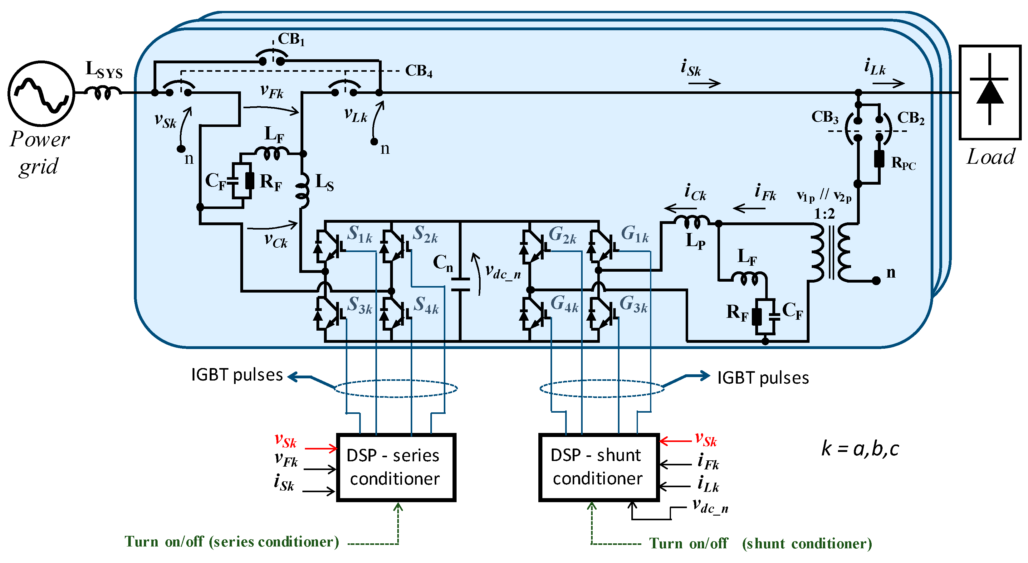
There are two main reasons for the proposed dual-DSP architecture. The first reason concerns on the UPQC developed topology, illustrated in
Figure 1, which is composed by 6 single-phase full-bridge converters (each phase with a back-to-back configuration), resulting in a total of 24 power switches (in the scope of this paper were used Insulated Gate Bipolar Transistors (IGBTs) as power switches). This characteristic makes unfeasible to drive all of the IGBTs with a single-DSP architecture, since it has a maximum of 16 PWM outputs. As presented in [
20], there is also the possibility to implement an architecture constituted by a master DSP with dedicated microcontrollers (slaves) to generate PWM signals to drive all the IGBTs. However, the main problem associated with this solution is the complexity and required time for the communication among the master DSP and the slave microcontrollers, limiting the sampling frequency and compromising the UPQC performance. The second reason was to exploit the advantage of a back-to-back configuration that can be independently controlled from each other, respecting some constraints. Indeed, respecting some constraints, it is possible to control independently the UPQC power conditioners. The first constrain consists of turning on the series conditioner after the shunt conditioner be turned on, considering that the shunt conditioner is responsible to keep the DC-link voltages regulated. The second constrain is related with the sequence to command the circuit breakers used to connect the UPQC to the power grid or to disconnect it. A detailed explanation about these constraints is presented in
Section 4. Using the proposed dual-DSP architecture results in a considerable decrement of the processing time to execute the control algorithms in each DSP, allowing increasing the sampling rate and, therefore, minimizing time-delay problems due to sampling effects, which are very common in digital control systems.
A summary involving the major topics of this paper is described as follows: Aspects related to the system configuration of the UPQC are illustrated in
Section 2; A set of equations describing the implemented algorithms is introduced in
Section 4; In
Section 4 are presented experimental results of the UPQC; The conclusions and suggestions for further work are presented in
Section 5.
2. Developed UPQC Prototype
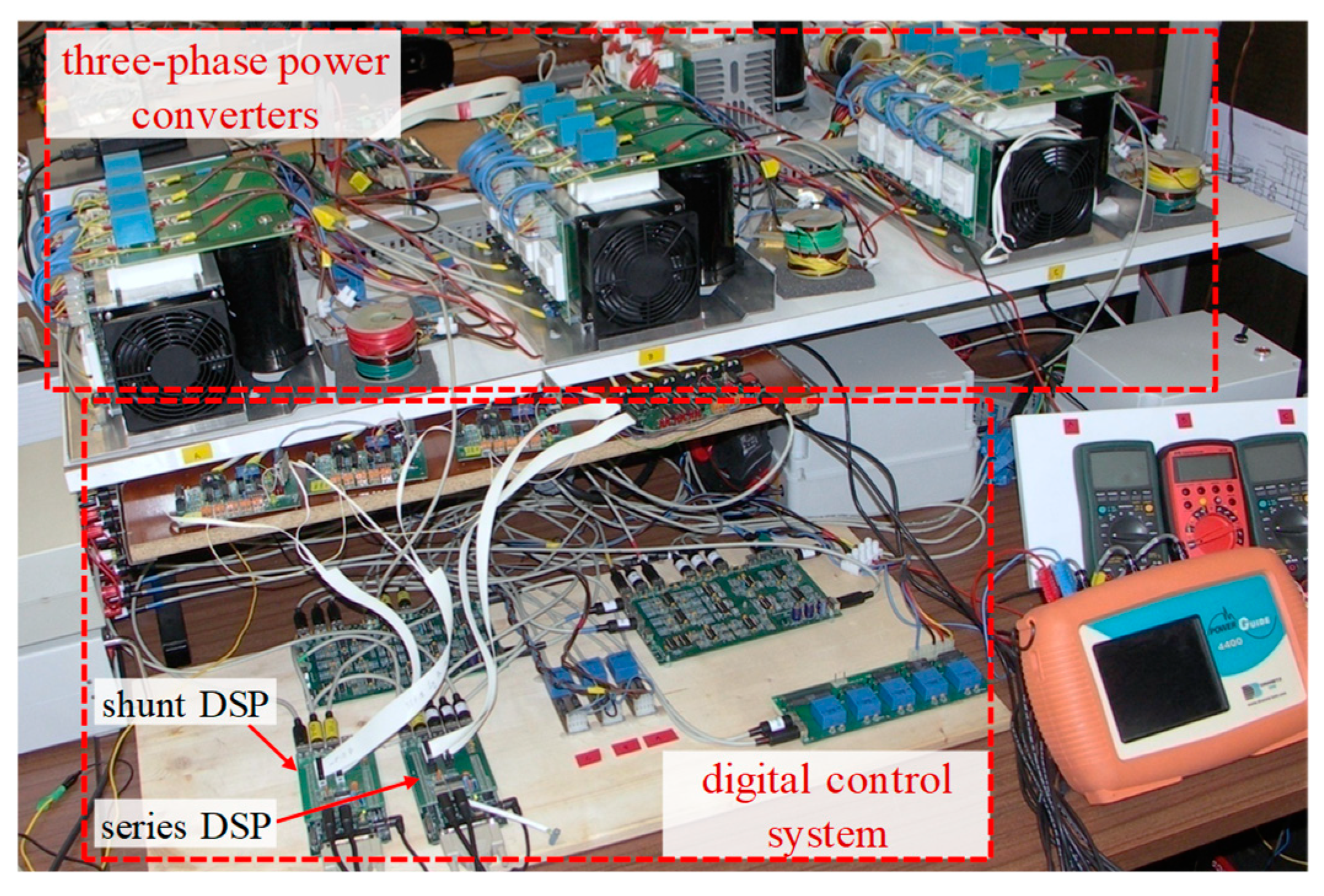
Figure 1 shows the single-phase electrical diagram of the UPQC connected into a three-phase three-wire system. Due to its modular topology, it was illustrated a single-line electrical diagram since the topology corresponds to three individually single-phase modules connected to a three-phase power grid. The developed UPQC prototype is shown in
Figure 2, where the power converters and the digital control platform are highlighted. As it can be seen, the power converter is constituted by three main modules, corresponding to the three-phases of the power grid, each one with a full-bridge for the series conditioner and with a full-bridge for the shunt conditioner. Therefore, six full-bridge modules (with a back-to-back configuration for each phase) comprehend the UPQC power converter, as indicated in
Figure 1. Each module corresponds to a single-phase, full-bridge Pulse-Width Modulation (PWM) converter, with four SKM50GB063D IGBTs (Semikron, Nürnberg, Germany). These IGBTs are designed for power switching applications, withstanding 600 V reverse voltages and currents up to 50 A.
Figure 1 also shows the signals
S1k,…,
S4k and
G1k,…,
G4k (
k =
a;
b;
c) to command the series and shunt conditioners, respectively.
A 5 kVA three-phase diode rectifier with ac inductors and with a RC parallel circuit at the DC side is used as the UPQC load. The developed UPQC was validated when connected to a power grid voltage with nominal value of 115 V. On the other hand, three single-phase transformers were applied (5 kVA, 115 V//57.5 V) to connect the shunt conditioner with the power grid. All of these transformers present a 5% leakage reactance and copper losses lower than 1%. It is important to note that the secondary side of these transformers is connected in wye, with the common point represented as n in
Figure 1. This common point is used as a reference to the power grid and to the load voltages.
Furthermore, there are circuit breakers applied to connect the UPQC to the power grid or to remove it in case of malfunction of the power converters. As illustrated in
Figure 1, the circuit breakers
CB1k and
CB4k are used to connect or to remove the series conditioner with the power grid, whereas
CB3k and
CB2k are used to connect or to remove the shunt conditioner. There is also a pre-charge resistor,
RPC_k to minimize the growing rate of the DC-link voltage when the shunt conditioner is connected to the power grid for the first time. A description about the UPQC start-up procedure is presented in
Section 4.
The DC-link of both conditioners is composed by three capacitors connected in parallel. All of these capacitors present a capacitance of 8200 µF and are able to support DC voltages up to 350 V. Second order RLC passive filters are applied to filter the high-frequency switching harmonics generated by the power converters. For both conditioners, these passive filters are represented as
LF (0.2 mH),
RF (200 Ω) and
CF (4.7 µF). The inductors represented by
LP and
LS are equal to 0.6 mH and 0.2 mH, respectively. Besides the second order RLC passive filters, other possibility is based on LCL filters as demonstrated in [
21,
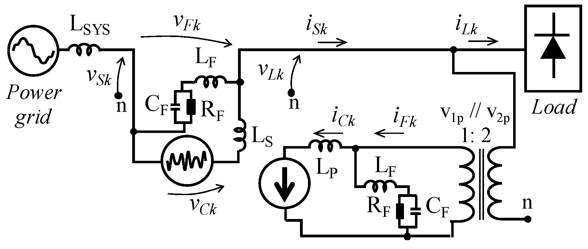
22]. However, this solution has as negative aspect related to the possible low-frequency resonances with the power grid impedance, which may result in system instability. Due to this condition, it is necessary to implement an algorithm capable of damping possible low-frequency resonances, improving the overall power grid stability, or use damping resistors. The transfer functions
VFk(s)/
VCk(s) and
IFk(s)/
ICk(s) were obtained considering the simplified circuit illustrated in
Figure 3.
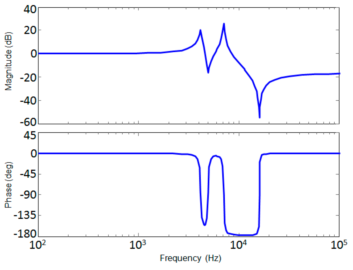
It must be referred that it has not been considered the model of the power transformer, since its parameter values are much smaller in comparison with the other passive elements of the circuit. Based on the transfer function of the series conditioner illustrated in
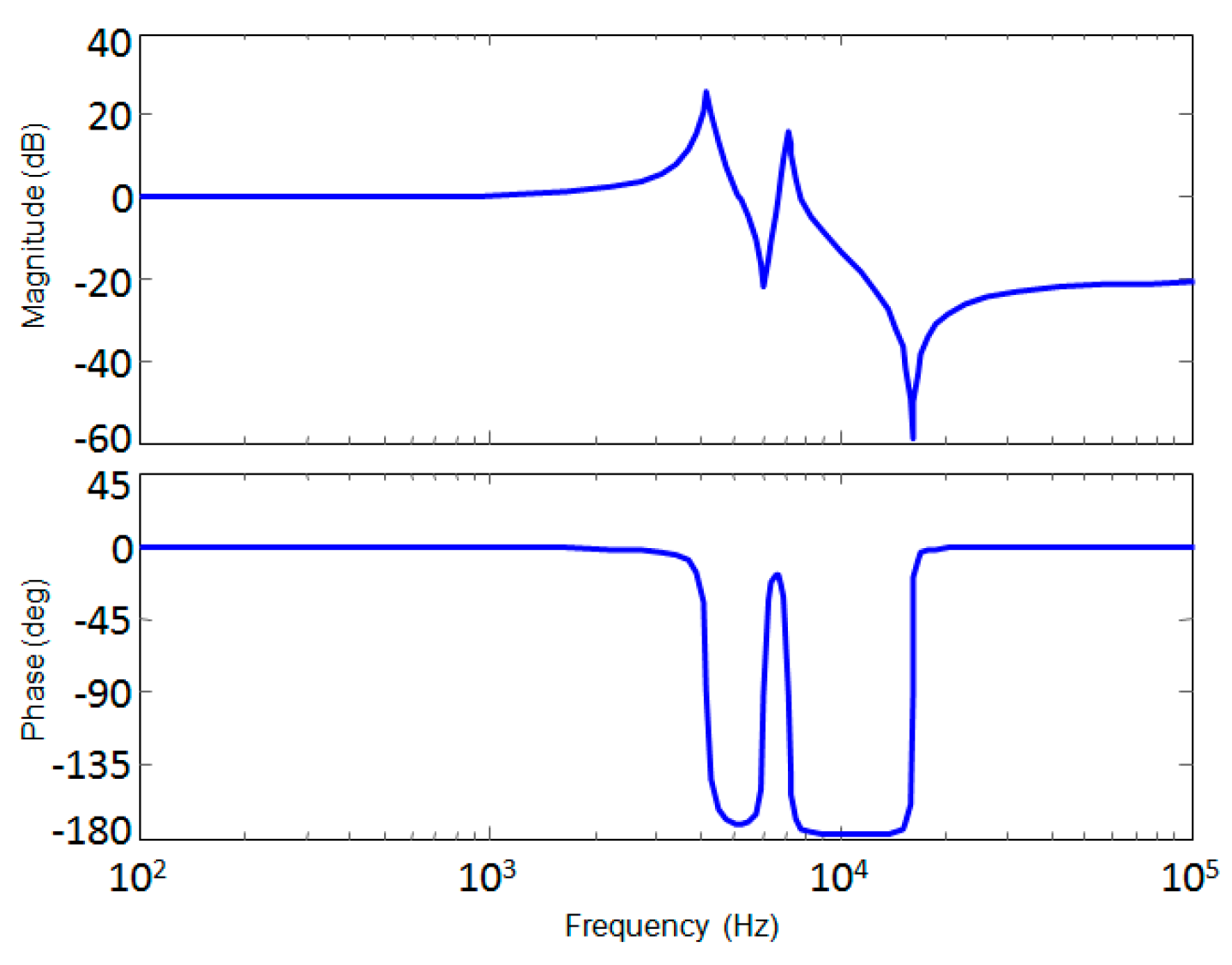
Figure 4, there are two resonance frequencies at 4.15 kHz and 7.04 kHz. At the switching frequency (16 kHz) occurs a gain of −55 dB and a gain of −17.1 dB to the frequencies above 16 kHz. On the other hand, the transfer function of the shunt conditioner (
Figure 5) presents resonance frequencies at 4.18 kHz and 7.07 kHz. There is gain of −59 dB at 16 kHz and −20 dB to the frequencies above 16 kHz. At both transfer functions, the low-frequency components (up to 1 kHz) present a gain of 0 dB and the phase angle is almost zero (less than 0.5°). It is worth to note that the series conditioner does not produce harmonic components in the range between 1.0 kHz until close to 16 kHz and the shunt conditioner may produce harmonic components in this range, however, with a very small amplitude. Thus, it is expected that the observed resonances do not result in any instability or resonance phenomena. Nevertheless, to increase the robustness of the system, it was implemented a damping controller, such that the series conditioner acts as a harmonic resistor to the harmonic components that may arise due to the resonance of the passive filters with the power grid impedance. This controller is similar to the ones introduced in [
23,
24].
3. Implementation of the Dual DSP Architecture
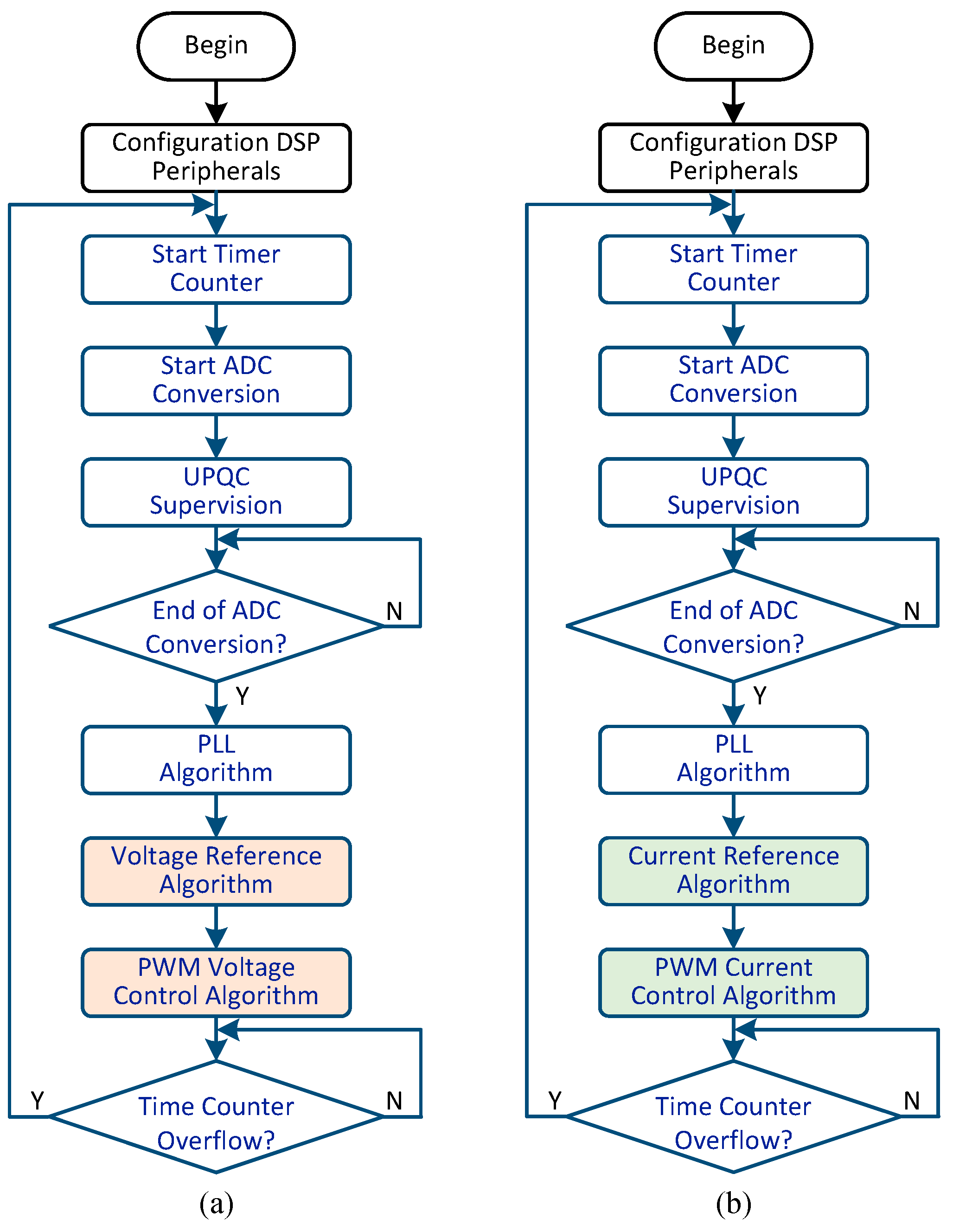
Figure 6 shows the structure of the control flowcharts about the implemented algorithms for the series (
Figure 6a) and shunt (
Figure 6b) DSPs. Both structures differ from each another only by the algorithms used to determine the reference signals and the PWM control. These algorithms and the phase-locked loop (PLL) demand the higher computational efforts, where the time period to execute the remaining algorithms is almost negligible (lower than 2 µs in a total of 31.25 µs available). A detailed explanation about the DSPs computational effort is presented in
Section 4.3.
Initially, all of the peripherals (ADCs, timers, interruptions and PWM) were configured. In sequence the timer counter is enabled and the ADCs start acquiring the new samples. Then, all of the generic definitions are loaded at the block diagram “UPQC Supervision”, and the interrupt routines, including the ADC conversion, were disabled. At this time, all of the internal control algorithms, included in the main function, are executed sequentially in an infinite loop. They are represented by the UPQC algorithms, and they are described in sequence. This process ends when the timer counter overflows, with the ADC converters enabled to acquire the new samples. The first algorithm corresponds to the PLL algorithm and it was implemented in both DSPs. It presents a similar structure of the α-β PLL [
25], together with a low-pass filter denominated as pseudo moving-average filter [
26,
27]. This low-pass filter, located between the phase detector and the loop filter, is given by:
where
x[
n] and
y[
n] correspond to the current input and output samples of the low-pass filter and
y[
n − 1] the previous output sample. The
J parameter can be understood as the damping factor of the filter, i.e., a high-value of
J results in an output signal presenting a small ripple and, on the other hand, the time period to reach the steady-state condition is increased.
In this case,
J was determined through preliminary simulations, taking into consideration the objective to damp possible oscillating components that may appear at the internal signals, due to presence of low-frequency harmonics or, in a worst condition, imbalanced components at the fundamental frequency. It is important to comment that it represents a low-pass filter requiring only one auxiliary variable and it is simple to implement. A moving-average filter implementation needs auxiliary arrays and demands a higher memory allocation, associated to the other internal arrays necessary to implement it. The internal RAM memory of the DSP is limited to 18 kB. Due to this reason, the pseudo-moving average filter was chosen. The PLL output signals correspond to unitary sinusoids in phase with the fundamental positive-sequence component of the power-grid voltages and they are given by:
where
is the position at the array of the PLL output signals that corresponds to a phase-shift of 120°. The conventional bilinear transformation was employed as the discretization method.
3.1. Reference-Current Algorithm
The reference currents are obtained using two different algorithms. The first one, based on the active- and non-active currents, determines the non-active currents drawn by the loads. These non-active currents are denominated as
iLq_k, with
k =
a;
b;
c. Since the output signals produced by the PLL were used to determine the active currents, it is important to highlight that, in this case, the active currents correspond to the current components that produces active power only with the fundamental positive-sequence component of the grid voltages. Basically, the active currents drawn by the load, with their amplitudes normalized, are determined as follows:
where
and
corresponds to:
The second algorithm is applied to keep regulated the DC-link voltages of the three single-phase back-to-back converters and they are denominated as
idc_1,
idc_2,
idc_3. These currents, with their amplitude normalized, are calculated as follows:
where
H(
z) corresponds to the discrete transfer function of the proportional-integral (PI) controller employed in this control algorithm, and
vdc* is the DC-link voltage reference. The PI parameters were tuned through preliminary simulations, submitting them to a range of different values, to identify the best combination that provides zero error at steady-state condition, without compromising the UPQC performance during the transients. After the execution of these two algorithms, the reference currents are determined as follows:
Other proposals, involving control strategies for active filters, can be found in [
28,
29]. Nevertheless, the control algorithms based on the active- and non-active currents have been chosen, since they are simple to be implemented in a DSP, with the shunt conditioner able to improve most of the power quality indices at the point where it is connected to the power grid.
3.2. Reference-Voltage Algorithm
This algorithm, executed in the DSP of the series conditioner, provides the features of active filtering, voltage regulation and system stability. The normalized reference voltage that is synthesized by the PWM control (
ref_k, for
k =
a;
b;
c) is given by:
Note that the calculation of the amplitude of the fundamental positive-sequence voltage is no longer necessary. Indeed, if the measured system voltage is normalized such that a unity amplitude represents its nominal value, this normalized voltage signal can be directly compared with the PLL output,
pllk, to achieve the compensating voltage references. In this case, the difference between the PLL outputs and the normalized voltages includes also sags or swells, as well as imbalances and distortions, which may be affecting the power grid voltages. A damping signal,
vHk, is applied to provide system stability. This algorithm was originally conceived to add a controlled resistance to the harmonic components of the grid currents, minimizing their flow through the power grid [
1,
24]. In this work this concept was extended to the non-active components of the grid currents, i.e., the damping controller provides a high-impedance path to all of the current components that do not produce active power with the fundamental positive-sequence component of the power grid voltages. In the scope of this paper, the sags or swells compensation can be performed until 20% of the nominal voltage. In the experimental validation, a set of loads were connected upstream the UPQC for validating the developed hardware and the control algorithm. Regarding the passive RLC filters used in the series compensator, a small voltage drops (below 1% of the nominal voltage) occurs due to the grid current when it flows through the coupling inductors. It should be noted that the reactive power consumption due to the coupling filters is below 1% of the reactive power consumed by the load. Based on the aforementioned prepositions, the damping signal, with its amplitude normalized, is given by:
where
G can be understood as a conductance to the resonance harmonics and
iSq_k corresponds to the non-active component of the power grid current and it is determined as follows:
The active current at the power grid side corresponds to iSp_k and is determined in a similar way as described to calculate iLp_k, with the load currents replaced by the power grid currents. Based on the proposed concept, the shunt conditioner corresponds to the only low-impedance path to the non-active components of the load currents and the power grid currents as well. Thus, indirectly, the damping algorithm improves the performance of the shunt conditioner. The structure of the damping algorithm is the same as that one applied to determine the non-active components, but with the grid currents as inputs.
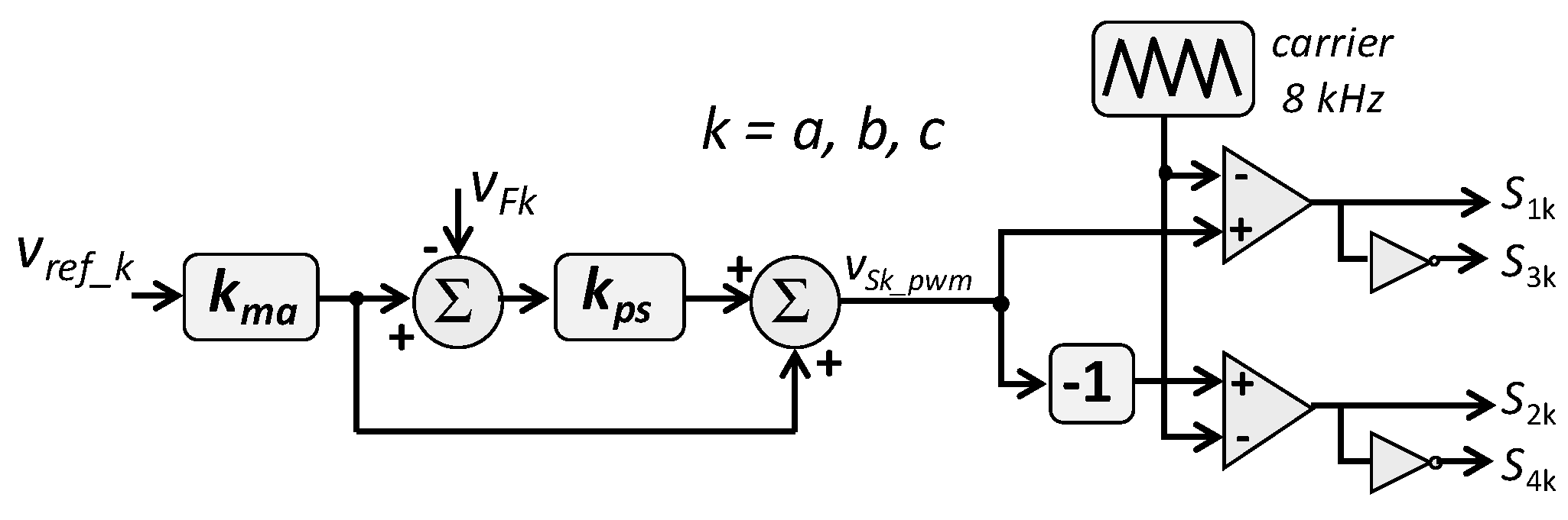
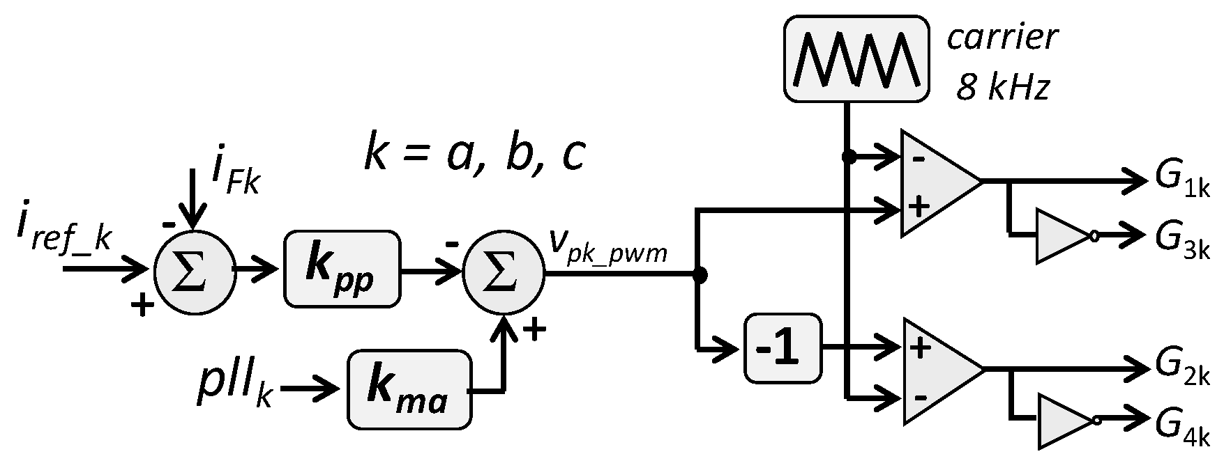
3.3. PWM Controllers
The PWM controllers for series and shunt conditioners are illustrated in
Figure 7 and
Figure 8, respectively. These switching techniques were applied since the corresponding algorithms are simple to be implemented with an acceptable performance in transient and steady-state conditions. In the literature there are proposals for multi-sampled current control as that introduced in [
30]. Nevertheless, to overcome the multi-sampling approach triggers nonlinear behaviors, it was linearized all of the system behavior and, as a consequence, its performance is compromised at transient events. Both PWM controllers are based on the unipolar PWM switching-technique, differing only in their structures to determine the reference signals that are compared with the triangular carriers. The outputs of these controllers are in accordance with the allocation of the IGBTs illustrated in
Figure 1. As illustrated in
Figure 7, the PWM control of the series conditioner is based on the feed-forward scheme. It presents as inputs the controlled voltages
vref_k (for
k =
a;
b;
c), and the voltages produced by the series conditioner,
vFk. The amplitude of these controlled voltages is normalized through a modulation index (
kma), which is given by:
The dynamic behavior of this modulation index provides to the series conditioner the capability to synthesize, adequately, the reference voltages, even when DC-link voltage oscillations occur. It is important to comment that this modulation index, based on Equation (9), can be applied if the input voltages and the triangular carriers amplitudes are normalized.
Figure 8 illustrates the PWM control of the shunt conditioner. Essentially, the voltage signal that is compared with the triangular carrier (
vpk_pwm) corresponds to control signals determined by the PLL circuit (
pllk), normalized by the index modulation (
kma), which is the same applied at “pwm voltage control” algorithm, plus the error between the reference current,
iref_k, and the current produced by the shunt conditioner,
iFk. It is important to mention that the inclusion of the control signal
pllk allows increasing the gain
kpp, which improves the performance of this PWM controller. Considering an expansion of the applied topology with more power converter cells in a cascade multilevel topology, there is a possibility to employ other switching techniques as the ones introduced in [
31,
32,
33]. Power converters based on multilevel converters are able to produce voltages and currents with a better resolution, at the expense of increasing the number of switches and, consequently, the complexity of the system.
4. Simulations and Experimental Results
In order to evaluate the UPQC performance considering the proposed dual-DSP control architecture, simulation and experimental results were obtained based on different test cases. It is expected that the developed UPQC be capable to compensate voltage and current harmonic content, correct the power factor and regulate the amplitude of the load voltages to their rated value. In sequence, it is presented an analysis involving the computational efforts of the DSPs in the proposed dual-DSP control architecture.
The start-up sequence to connect the UPQC to the power grid presents the following steps. The shunt conditioner was the first to be connected, with the circuit breaker CB2k closed to pre-charge the DC-link capacitors. In sequence, CB3k was closed and CB2k opened. At this condition, the shunt conditioner is able to be turned on. With the shunt conditioner turned on and at steady-state condition, it is initialized the start-up procedure to connect the series conditioner. All of the upper IGBTs (S1k, S2k) are turned on, and the circuit breaker CB4k was closed. In sequence, CB1k was closed and CB4k opened. At this condition the series conditioner is ready to be turned on, completing the entire UPQC start-up sequence.
4.1. Simulation Results
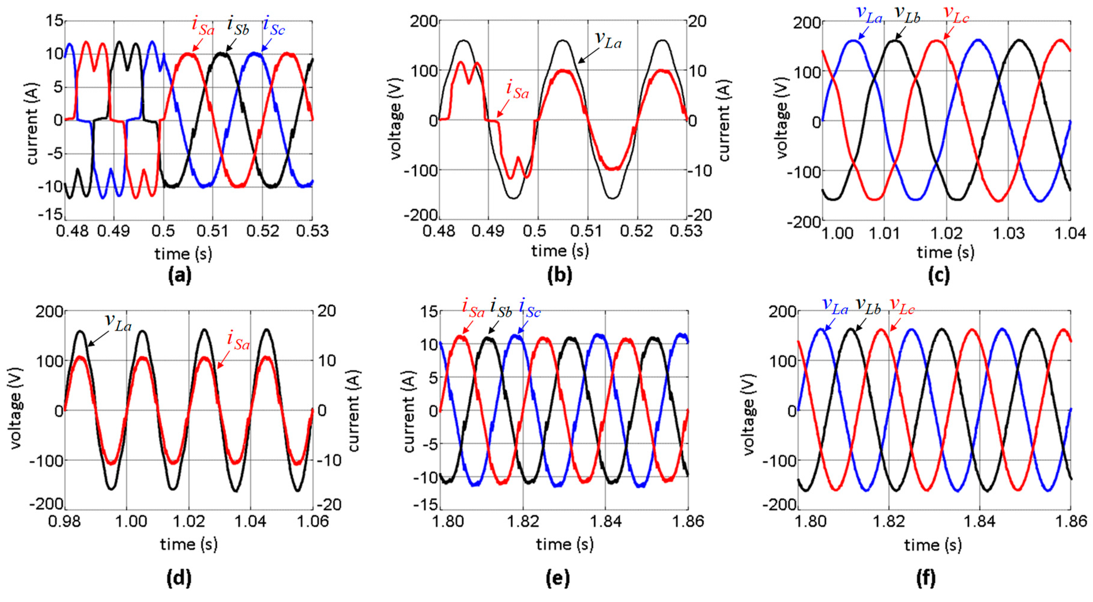
A test case was performed to evaluate the UPQC performance. Basically, in this test case, the shunt conditioner compensates the reactive power and current harmonics, whereas the series conditioner compensates voltage harmonics, with the shunt conditioner turned on at
t = 0.5 s and the series conditioner at
t = 1.02 s. At the time transient, when the shunt conditioner was turned on (
Figure 9a), the current harmonics were compensated, with the total harmonic distortion at the power grid currents reduced from 30% to 4.8%. Furthermore, it can also be noted that the high-frequency components produced by the shunt conditioner were entirely drawn by the passive filters (
Figure 9b). Otherwise, it would appear high-frequency components at the load voltage with the shunt converter turned on. In sequence, with the shunt conditioner under steady-state, the series conditioner is turner on at
t = 1.02 s (
Figure 9c). One cycle period after, the load voltages reach their new steady-state condition, with their total harmonic distortion reduced from 5% to 1%. Based on the simulation result shown in
Figure 9d, it can be noted that both converters work correctly, with one converter not compromising the performance of the other converter. The steady-state performance of the shunt- and series- conditioner are illustrated at
Figure 9e,f, respectively.
4.2. Experiemntal Results
The experimental results are based on two main test cases. The first one is similar to the already introduced at the simulation results, and the second test case shows the performance of the series conditioner compensating a voltage imbalance. However, before illustrating these test cases,
Figure 10 and
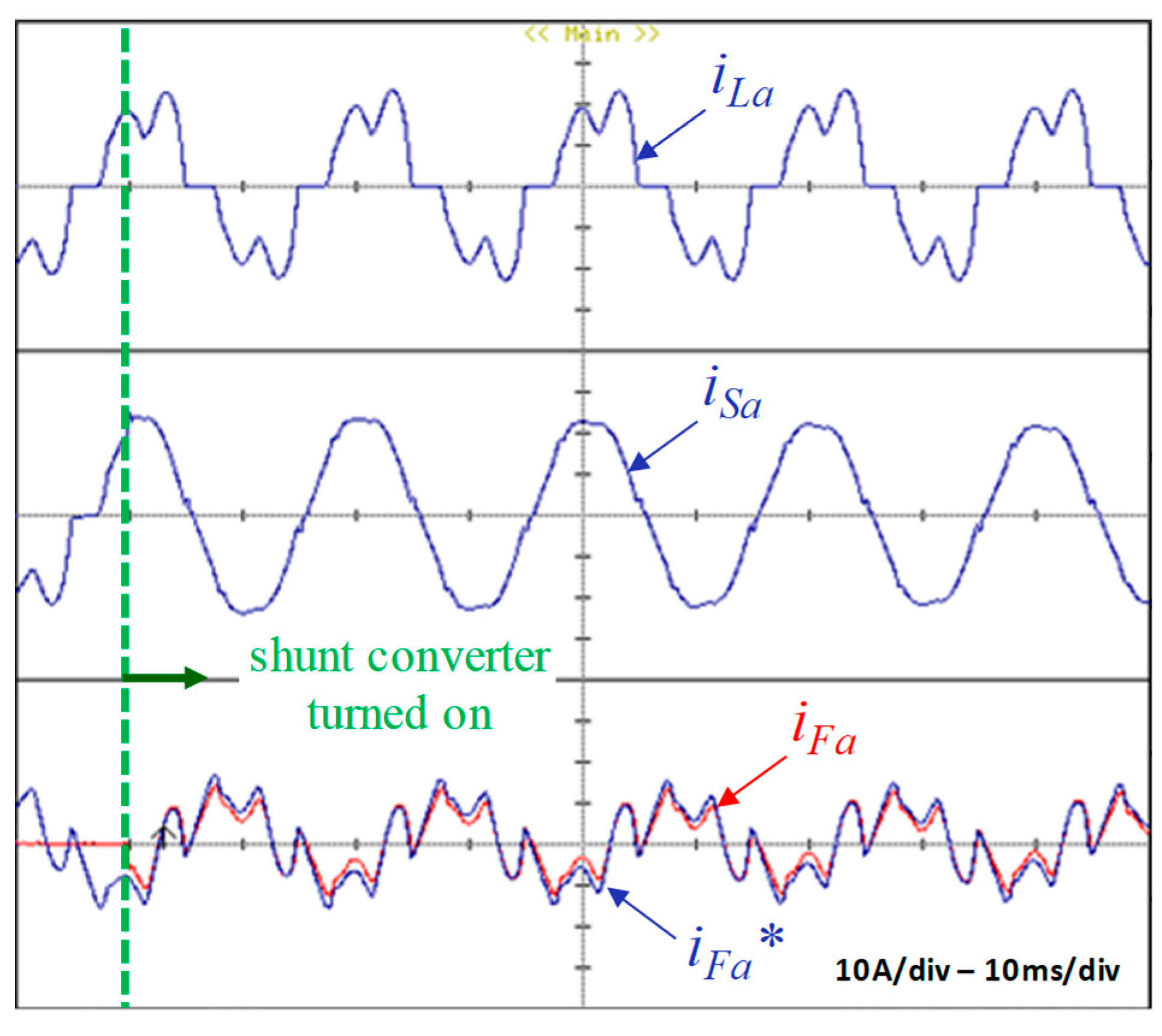
Figure 11 show, respectively, the performance of the PWM current and voltage controllers. When the shunt conditioner is turned on (
Figure 10), the produced current,
iFa, tracks the reference current,
iFa*, such that the compensated current,
iSa, is comprised by the fundamental positive sequence of the load current,
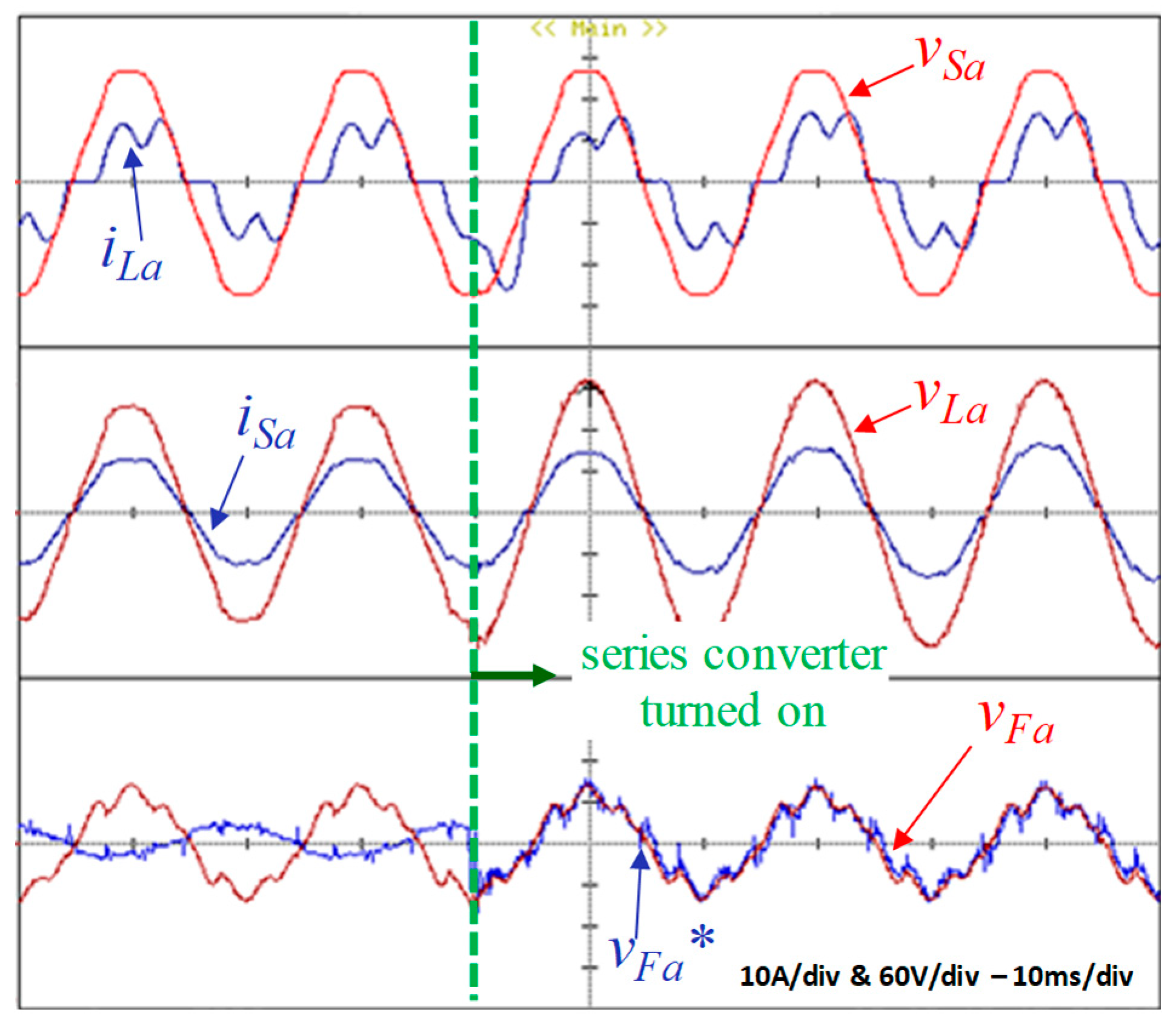
iLa, plus an active current necessary to regulate the DC-link voltage. When the shunt conditioner is operating in steady-state condition, the series conditioner is turned on (
Figure 11). At this time instant, the command that kept turned on the upper IGBTs of the series conditioners is disabled. When the series converter is turned on, the voltage produced,
vFa, tracks the reference voltage,
vFa*, with the load voltage,
vLa, corresponding to the fundamental positive-sequence of the power grid voltage,
vSa.
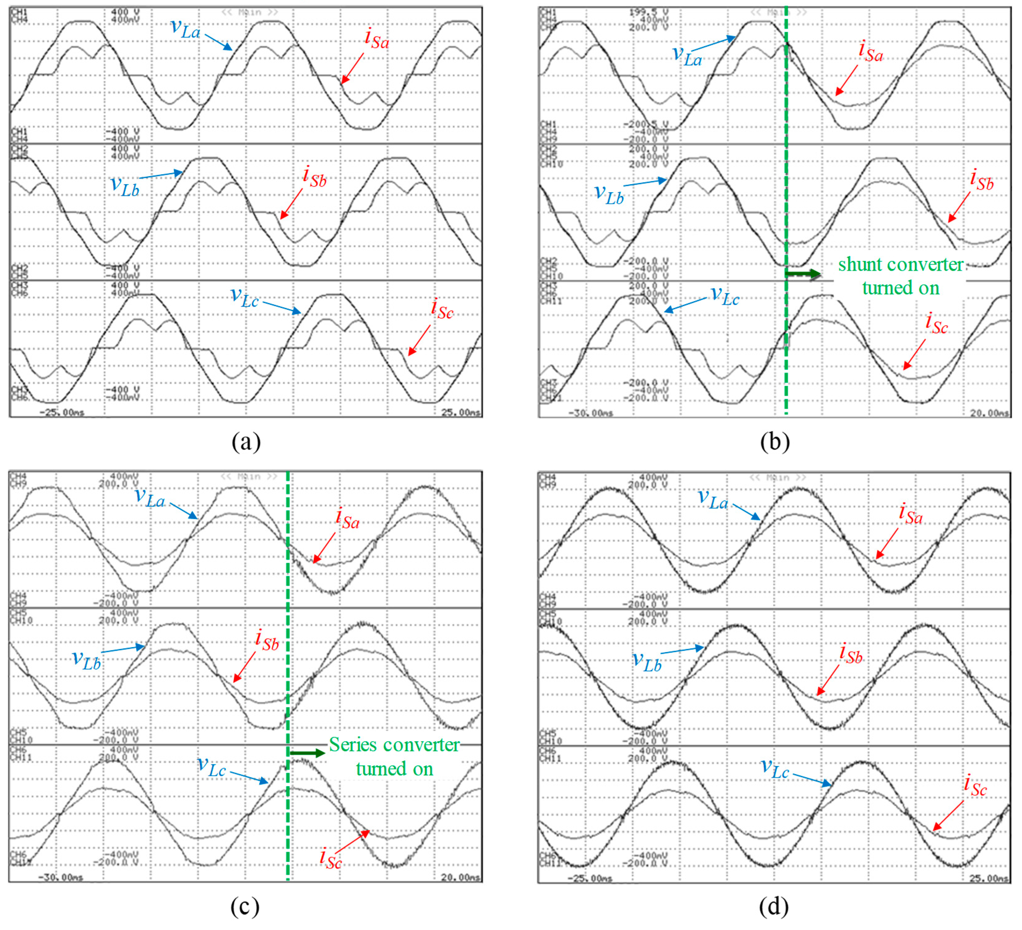
In sequence is illustrated the experimental results based on a case example, where the load voltages are balanced, regulated and with a harmonic distortion of 5%, whereas the load currents are balanced with a harmonic distortion of 29.2%, and the power factor is equal to 0.92. Initially,
Figure 12a illustrates the load voltages and the grid currents with the series and shunt conditioners of the UPQC turned off. In sequence,
Figure 12b shows the transient event when the shunt conditioner is turned on. In this test case the DC-link voltages were previously charged to their rated value and, due to this reason, it occurs a small transient increment of 1.5 A (rms value) in iSa when the shunt conditioner was turned on. The harmonic distortion was reduced from 29.2% to 6%.
Figure 12c shows the transient event when the series conditioner is turned on. It can be noted a very smooth transient, with the harmonic distortion reduced from 5% to 2.2% and the amplitude kept regulated. Moreover, with the series conditioner turned on, the harmonic distortion at the power grid currents was decreased from 6.0% to 5.5%, improving the performance of the shunt conditioner. The UPQC performance under steady-state condition is illustrated in
Figure 12d. In this condition, the harmonic contents at the grid currents and load voltages were reduced, the power factor was compensated and the rms values of the load voltages were increased to their rated value.
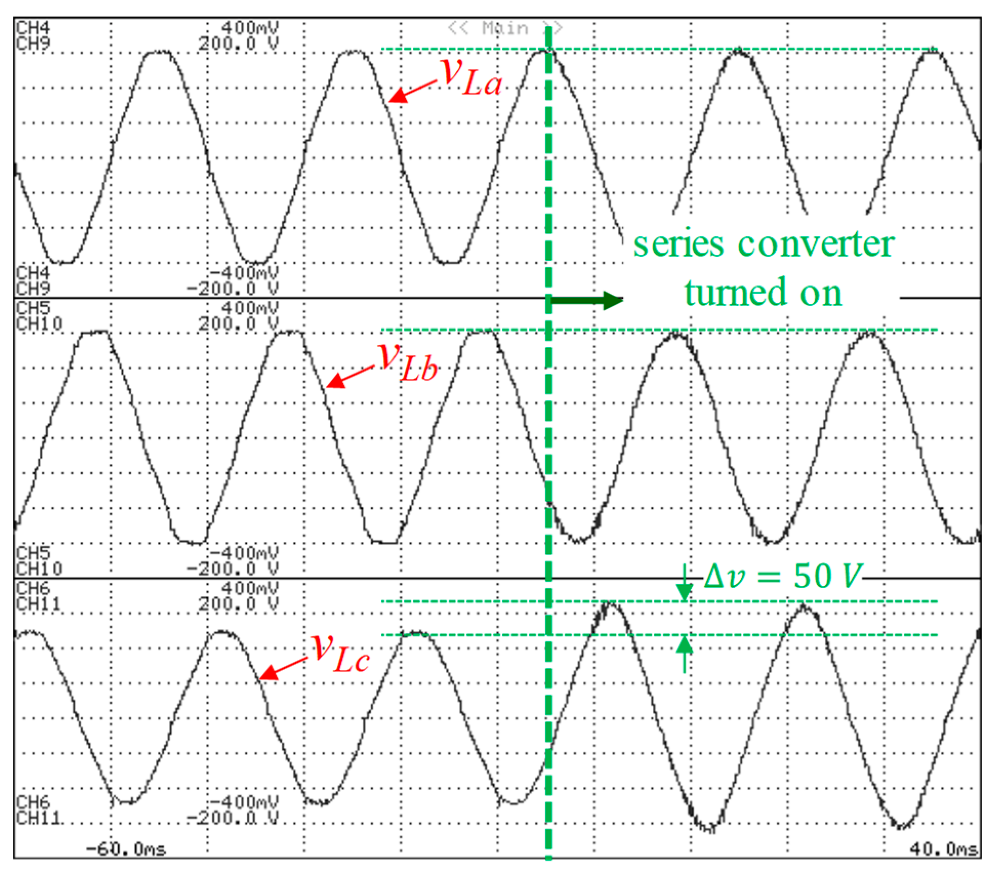
Furthermore, with the UPQC turned on, the active power provided by the power grid increases from 3.65 kW to 3.78 kW, due to the UPQC power losses, which corresponds to 130 W (3.5%) of the original active power, with the UPQC turned off. Under steady state condition, the shunt converter compensated nearly all the 5th and 7th harmonics (more than 90%). Regarding to the other harmonic currents the shunt conditioner compensated 72% of the 11th harmonic, 67% of the 13th harmonic, 59% of the 17th harmonic, 57% of the 19th harmonic, 46% of the 23th harmonic and 42% of the 25th harmonic. The other harmonic components are negligible. In relation to the power grid voltages, the harmonic components are comprehended by the 3rd, 5th and 7th harmonics, due to the single-phase nonlinear loads connected to the power grid. Under steady-state condition, the series conditioner compensated 85% of the 3rd harmonic, 91% of the 5th harmonic and 83% of the 7th harmonic. A second test case was introduced to evaluate the performance of the series conditioner compensating voltage imbalance (
Figure 13). In this test case, in a time period lower than half cycle-period, when the series conditioner was turned on the rms value of the load voltage,
vLc, was increased from 91 V to 115 V, indicating a fast response of the series conditioner. The other load voltages were already regulated, such that their rms values were kept constant. Furthermore, the harmonic distortion was reduced from 5% to 2%. Again, it can be noted a very smooth transient when the series conditioner was turned on.
4.3. Computational Effort of the DSPs
The computational effort needed to implement the aforementioned control algorithms is also notoriously important, to increase the performance of the UPQC, as well as to increase the switching frequency of the power converters that constitute the UPQC. Basically, there is a commitment to employ control algorithms demanding low computational effort without compromising the capacity of the UPQC to compensate power quality problems [
34]. The platform used to assess the computational effort of the control DSPs of the UPQC was the TMS320F2812F, a fixed point 32-bit DSP from Texas Instruments. All the input signals were sampled at a fixed rate of 32 kS/s, which corresponds to an interval of 31.25 µs between samples. Furthermore, since the fundamental frequency of the input signals is equal to 50 Hz, the fundamental component of the digitalized signals presents 640 samples per cycle period. In order to determine the time required for executing each one of the algorithms, it was measured the number of CPU clock cycles necessary to execute each routine. The required memory space necessary to execute the routines was also evaluated. As indicated in
Table 1, the required memory space to execute the routines of the DSP of the series conditioner is higher in comparison with the DSP of the shunt conditioner, this is due to the low-pass digital filters used to extract the average value of the measured voltages. Based on the preliminary experimental results, it was observed that the performance of the series conditioner was improved with these low-pass filters. Considering the execution time index indicated in
Table 2, it can be noted a similarity of the overall time period to execute all of the algorithms, indicating a good distribution of the algorithms burden in the DSPs. Furthermore, assuming a condition to embed all of the algorithms into a single DSP, it would result in an execution time of 44 µs (approximately), which would lead to a maximum sampling frequency close to 20 kHz. This reduction of the sampling frequency compromises the UPQC performance due to loss of information at the analog-to-digital conversion. One important issue involving real-time controllers for power electronics applications concerns the capacity of acquiring the highest number of samples per cycle. It minimizes inherent problems as, for example, introduction of phase-delay due to the sampling process. In this case, the decrease of the sampling frequency increases the phase delay of the sampled signal. Furthermore, as described in [
35], other negative aspect concerns on the PWM control bandwidth of the low-frequency gains, which becomes considerably limited.
Moreover, as aforementioned in the
Section 1, one must note that considering a single DSP to run all of control algorithms, a master-slave platform should be implemented. In this case, there is also the time delay related to the communication process among the DSP (master) with dedicated microcontrollers (slaves) to generate PWM signals to drive all the IGBTs. Finally, there is also a time delay necessary to assure that the series –and shunt PWM-signals are synchronized. In [
20] was implemented a digital controller for a multilevel STATCOM comprehended by DSP-based master with a multiple number of slave DSP –and FPGA-boards. In that case there was the time delay consisted on 40 µs to process all of the control algorithms, together with the communication system with an additional time delay of 29 µs. Therefore, this configuration leaded to an overall time-period of almost 70 µs.
Thus, considering a scenario, involving power converters applied for harmonic compensation, it can be noted how crucial that issue is. In this work, with the proposed dual-DSP control architecture, the harmonic components are within the accepted levels according to the IEEE 519-2014 Standard [
36].
5. Conclusions
A dual-DSP control architecture for a three-phase Unified Power Quality Conditioner (UPQC) is proposed in this paper, and a set of experimental results based on two test cases are presented and discussed. Through the obtained results, it can be verified the UPQC performance when compensating the main power quality problems commonly present in the power grid, proving the advantages of the UPQC as a contribution for smart grids. Moreover, it can also be verified the proper operation of the UPQC when controlled by the proposed dual-DSP architecture. In fact, distributed algorithms into a dual-DSP architecture constitutes a feasible solution to improve the performance of power conditioners presenting a back-to-back configuration. The obtained results also show that the proposed dual-DSP control architecture represents an interesting approach, mainly, due to the independence of the series and shunt conditioners, i.e., considering that there is a PLL algorithm at each one of the DSPs. Indeed, this solution contributes to improve the performance of active power conditioners and, furthermore, it also enables the possibility of adding other functionalities, which are crucial to deal with the new power quality issues, particularly those involving the active converters interfacing renewable energy sources, plug-in battery charging systems for electric vehicles, and to the distributed energy generation.


 ,
, 


