Investigation on the Resonant Oscillations in an 11 kV Distribution Transformer under Standard and Chopped Lightning Impulse Overvoltages with Different Shield Placement Configurations

 ,
,
Abstract
:1. Introduction
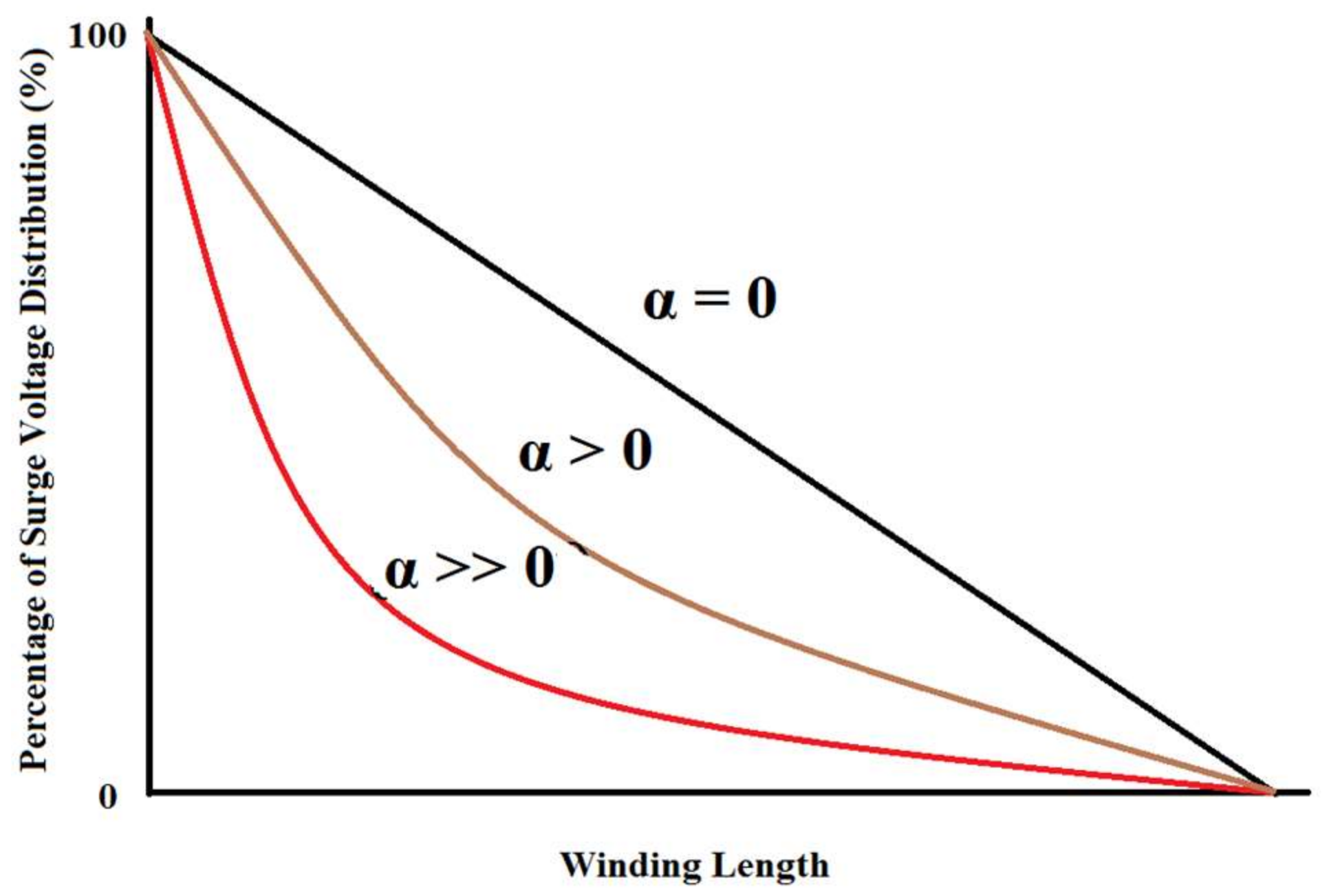
2. Resonant Overvoltage in Transformer Winding
3. Methodology
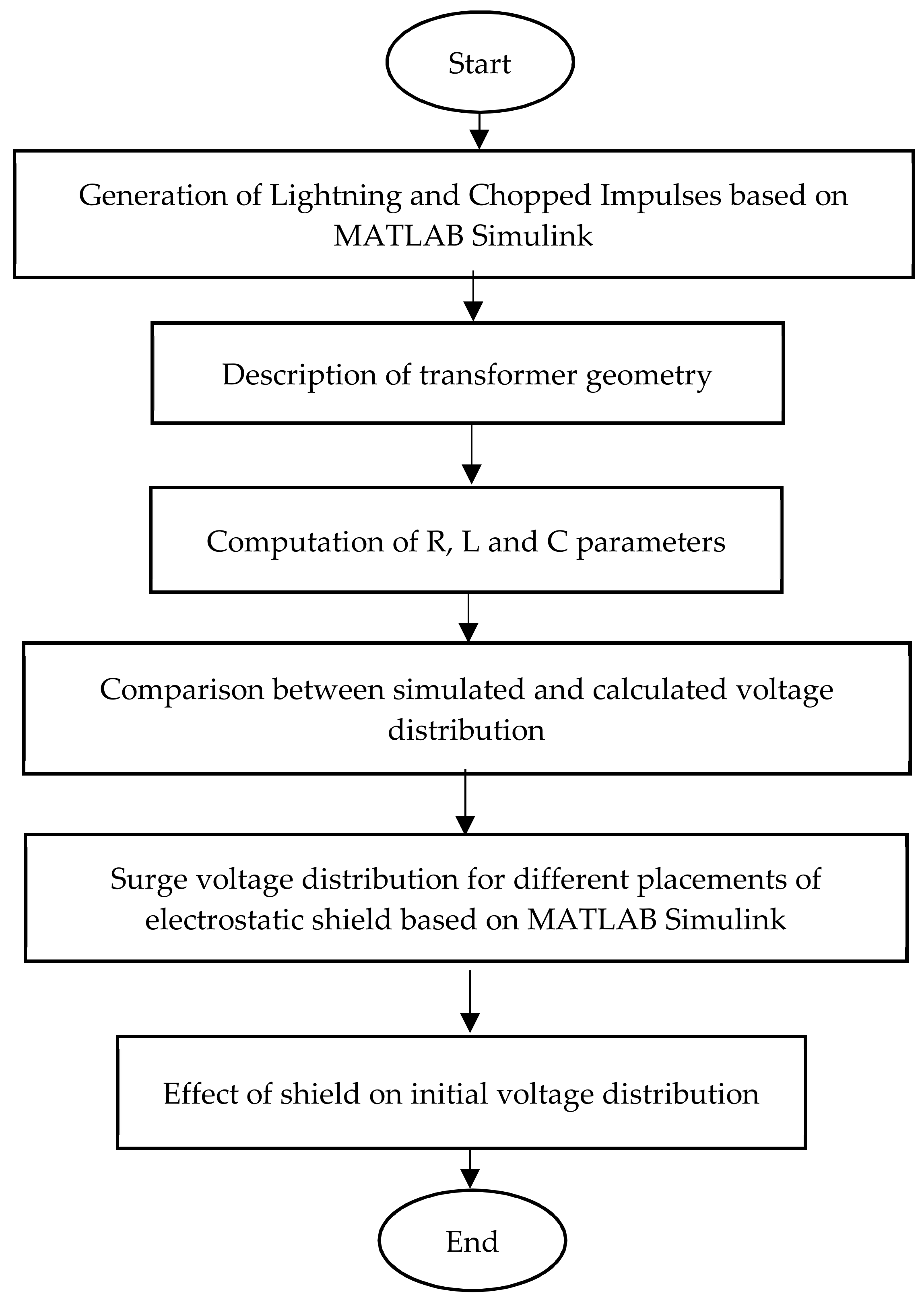
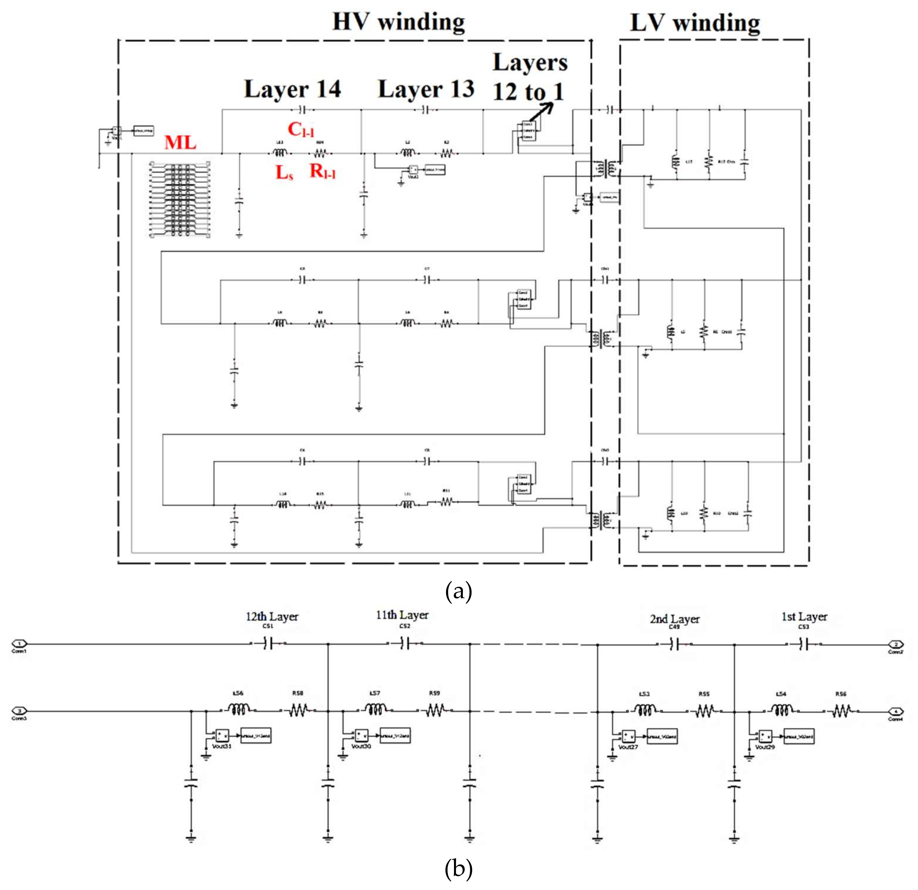
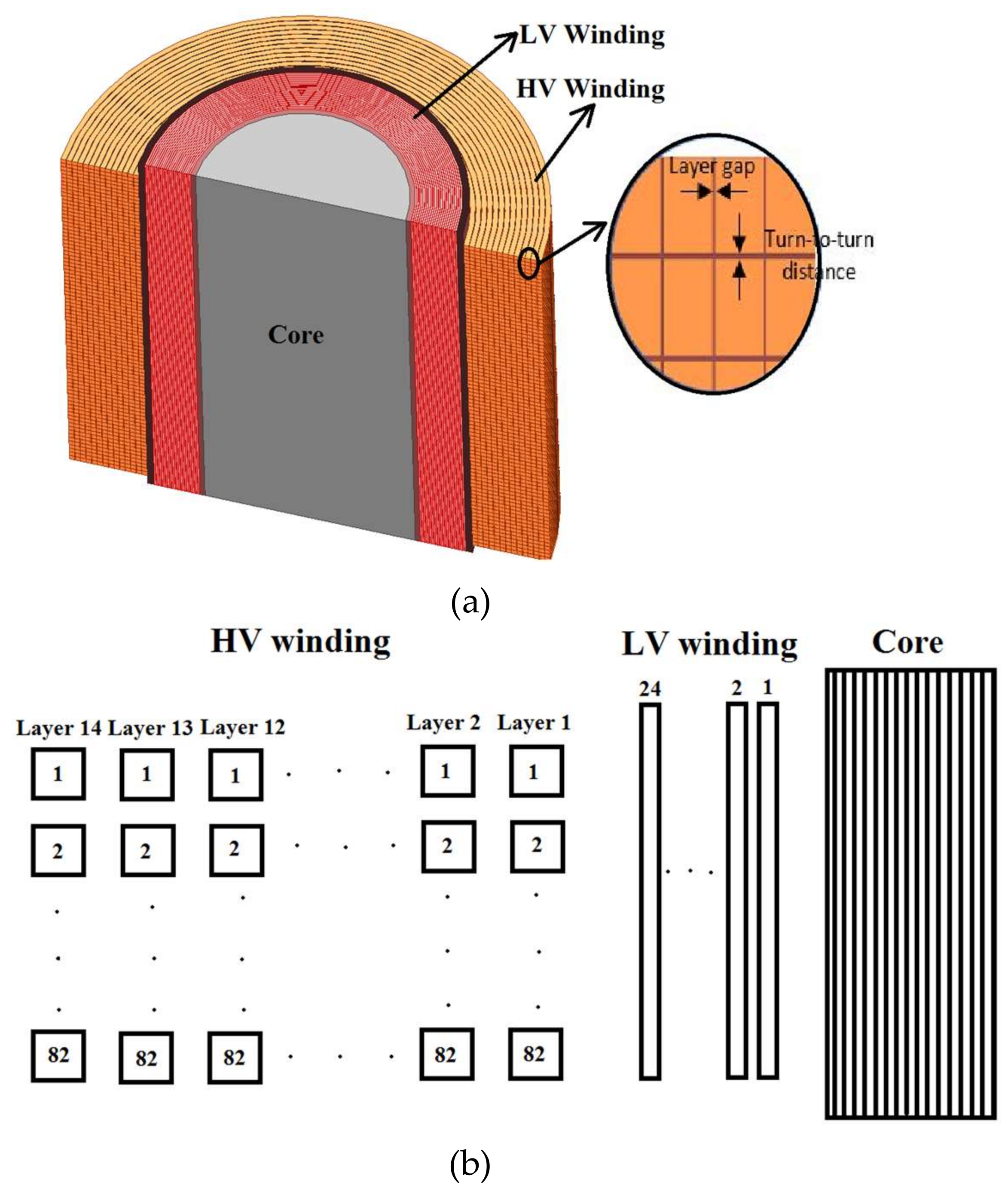
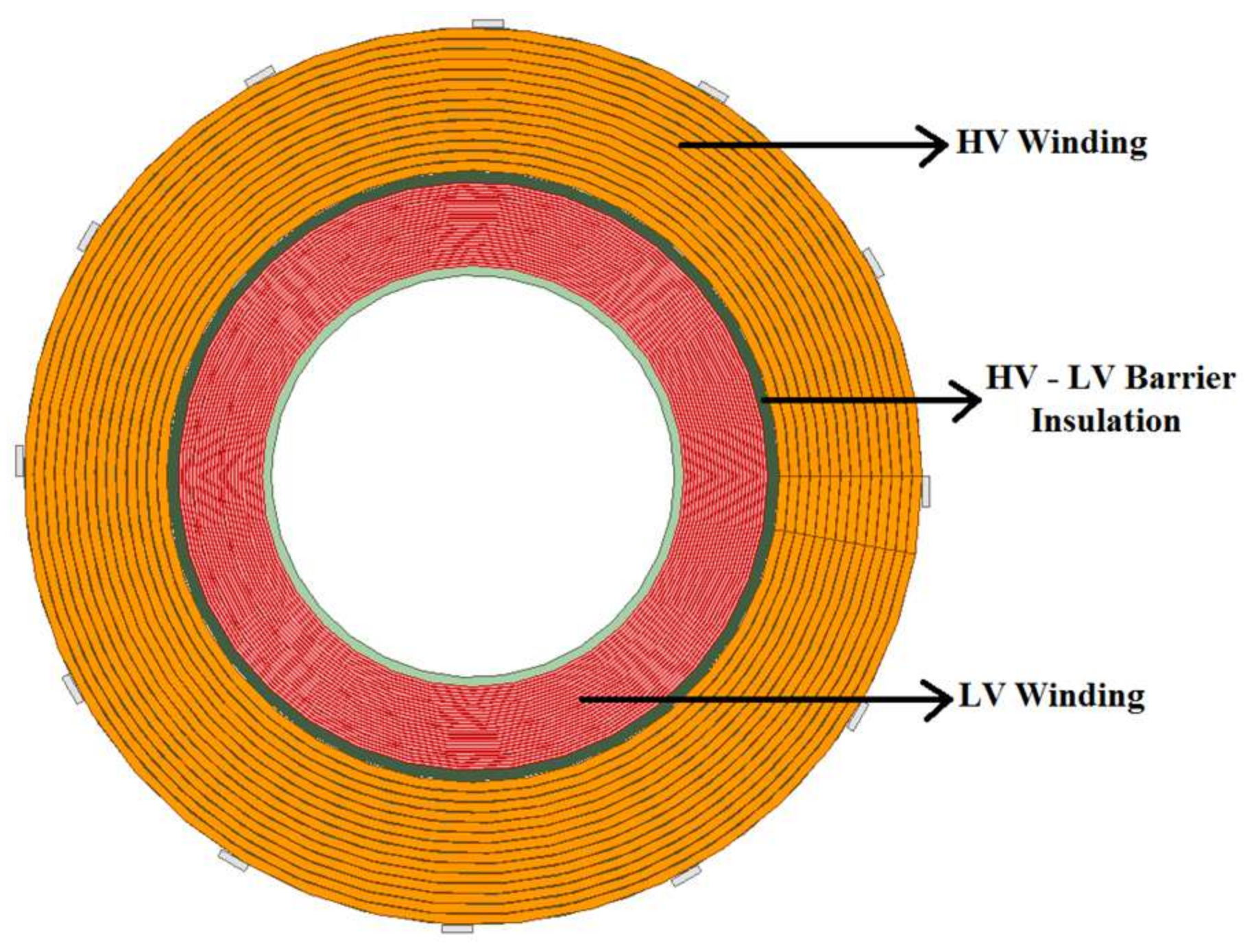
3.1. The Overall Framework of The Modeling of Transfomer Winding
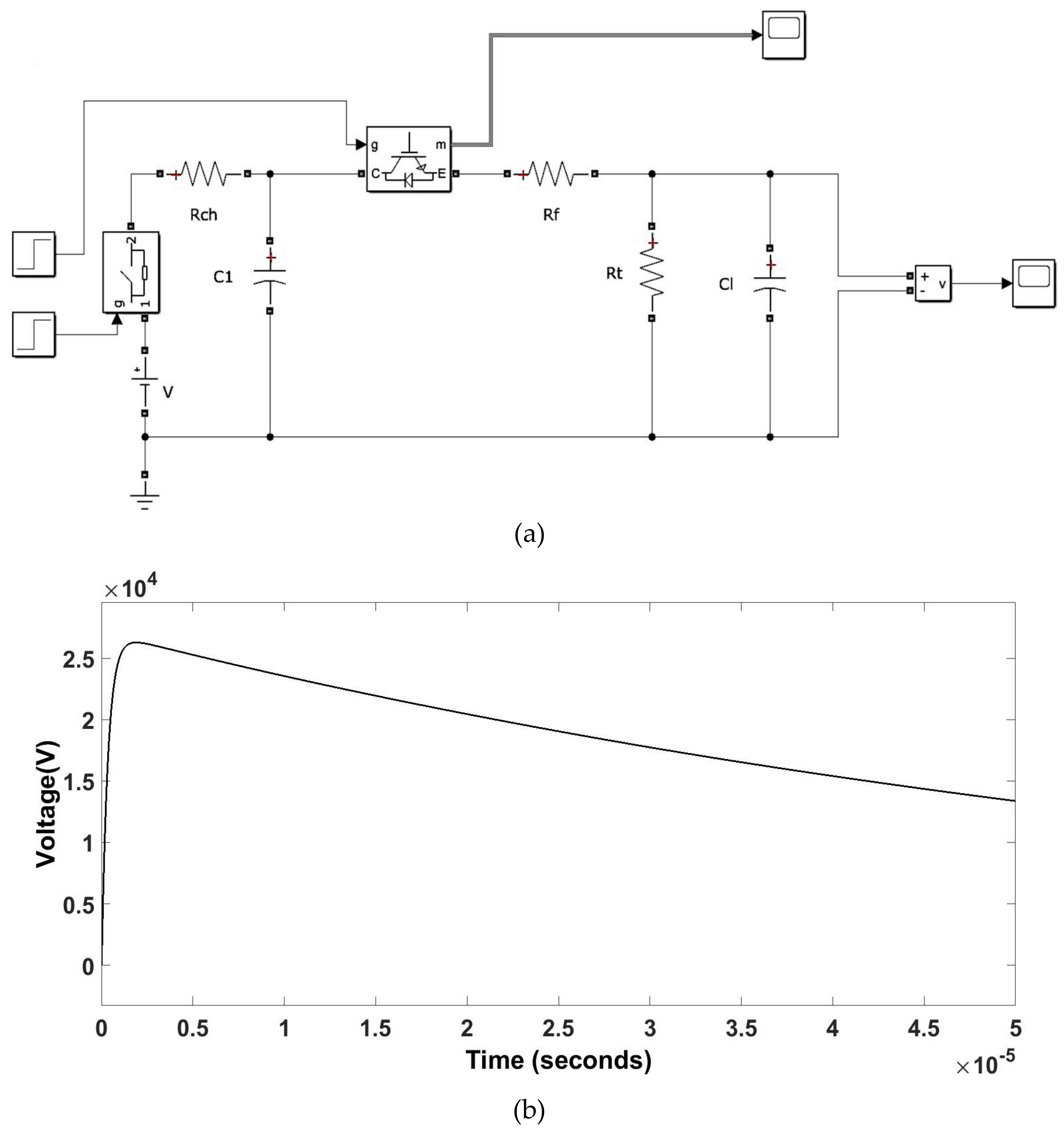
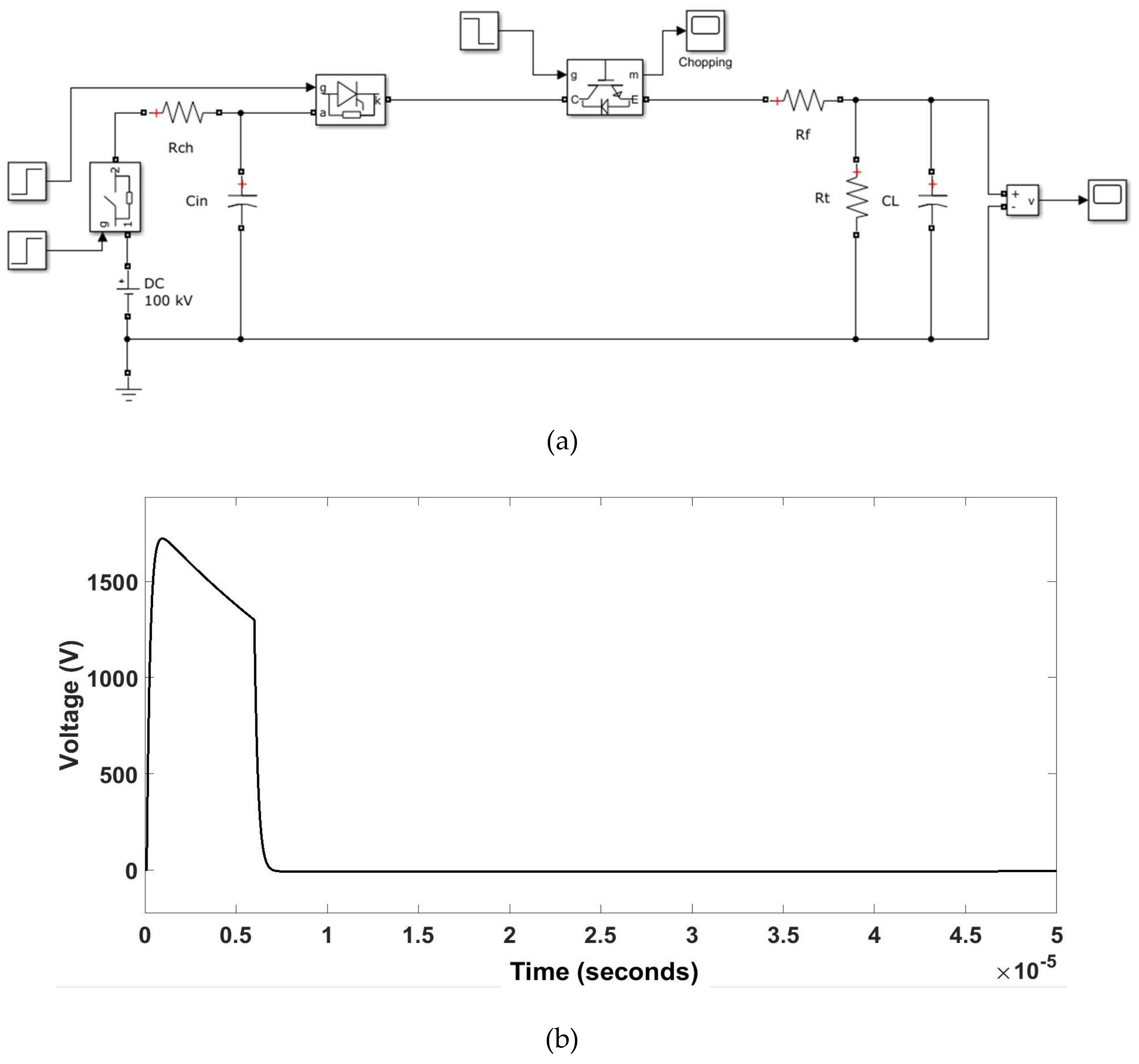
3.2. Generation of Standard and Chopped Lightning Impulse Voltage
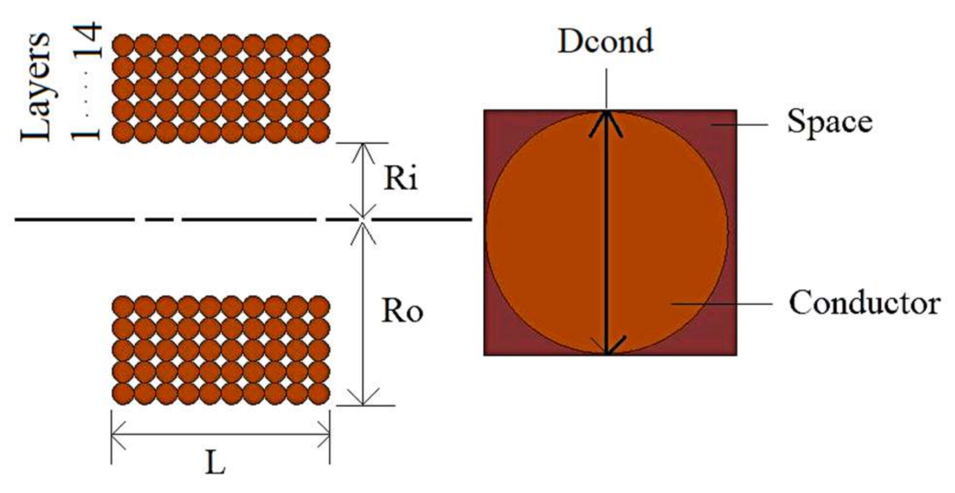
3.3. Calculation of RLCM Parameters
3.3.1. Calculation of Inductance
3.3.2. Calculation of Resistance
3.3.3. Calculation of Capacitance
3.4. Transformer Model
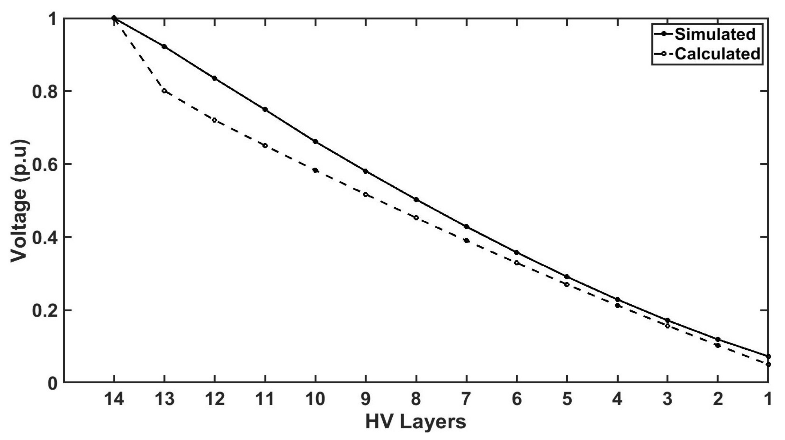
3.5. Comparison between Simulated and Calculated Voltage Distribution
3.6. Case 1: Transformer Model with Shield Placement between Layer 14 and Layer 13
3.7. Case 2: Transformer Model with Grounded Shield Placement between Layer 14 and Layer 13
3.8. Case 3: Transformer Model with Shield Placement between Layer 14 and Layer13 and between Layer 13 and Layer 12
3.9. Case 4: Transformer Model with Shield Placement between HV and LV Winding
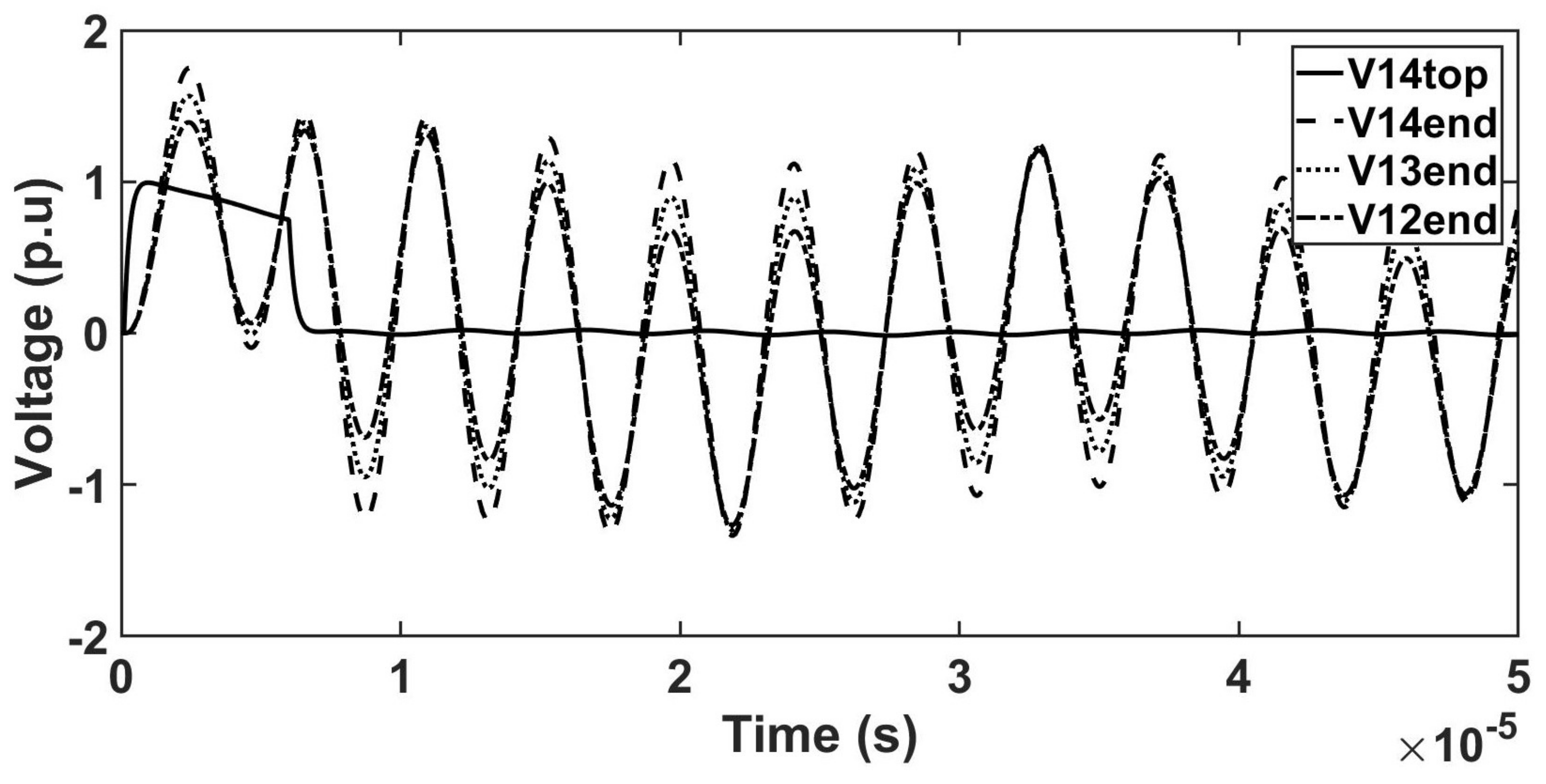
4. Results
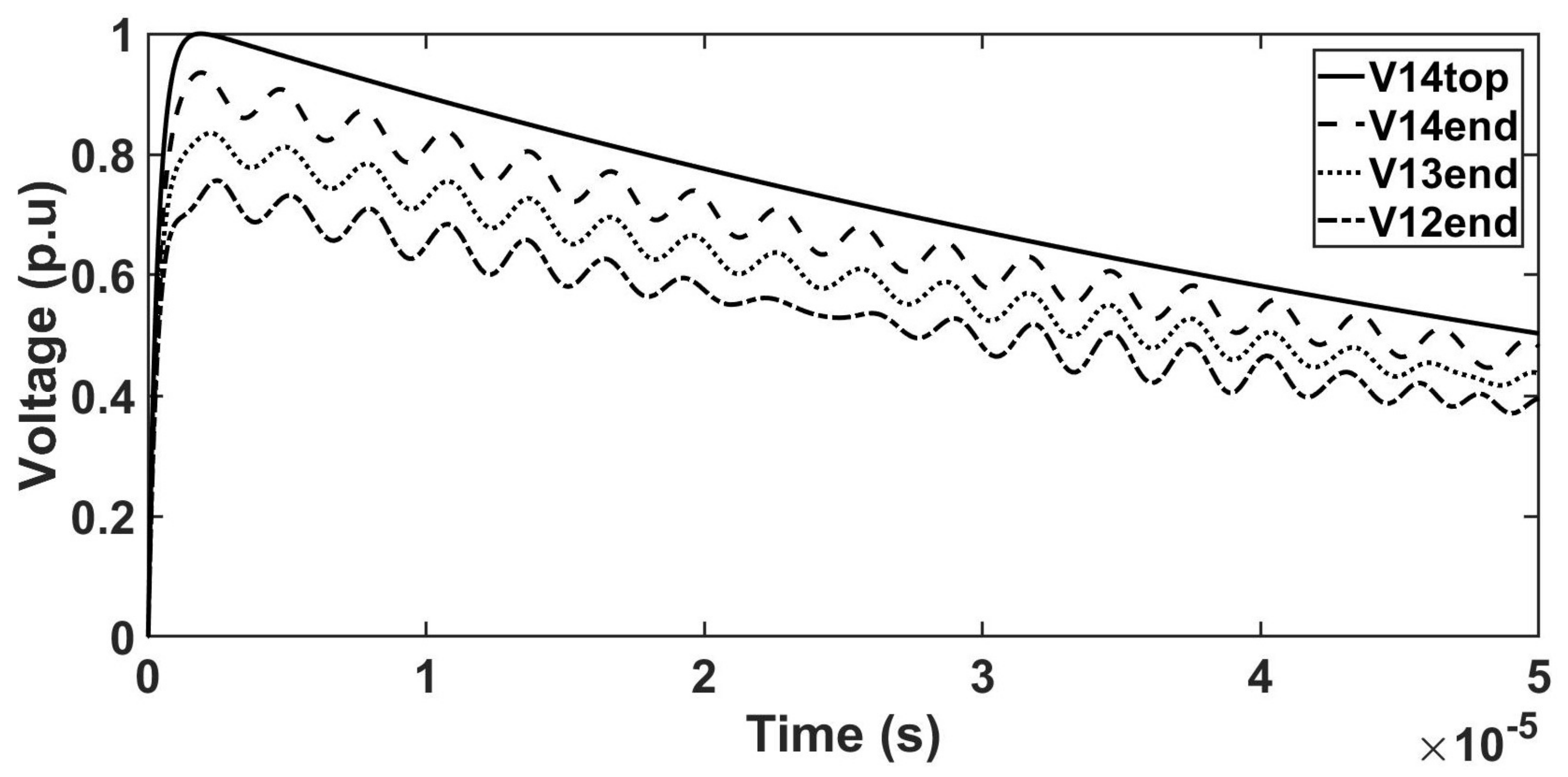
4.1. Surge Voltage Distribution under Standard Lightning Impulse
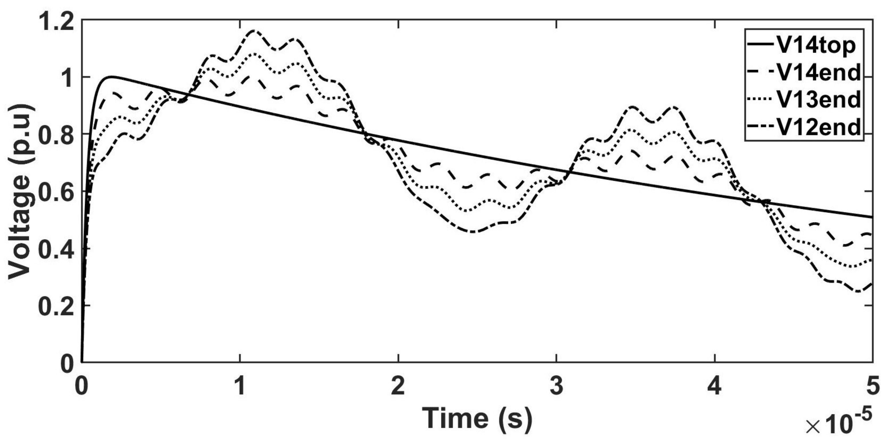
4.1.1. Case 1: Surge Voltage Distribution for the Transformer Model with Shield Placement between Layer 14 and Layer 13
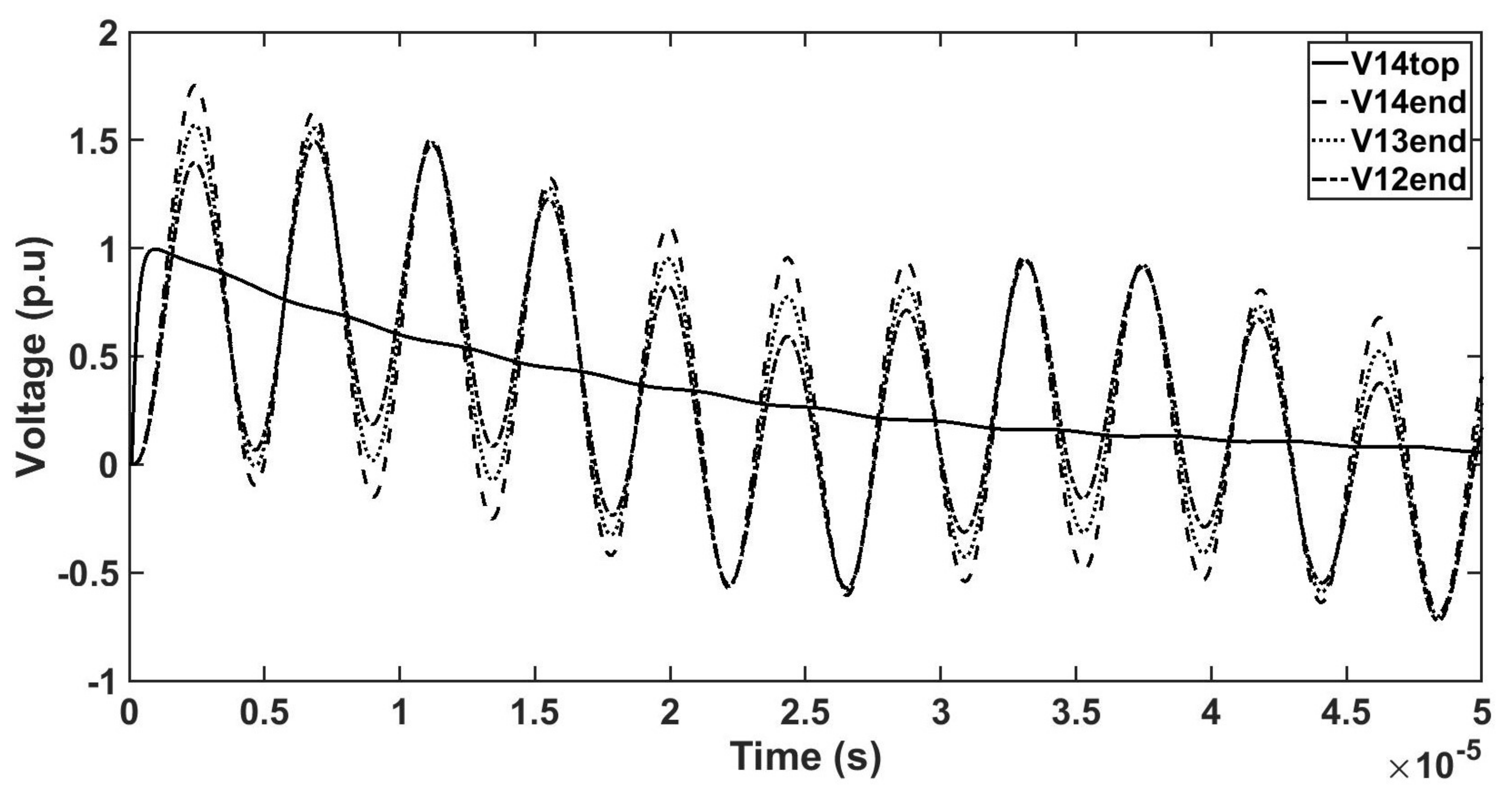
4.1.2. Case 2: Surge Voltage Distribution for the Transformer Model with Grounded Shield Placement between Layer 14 and 13
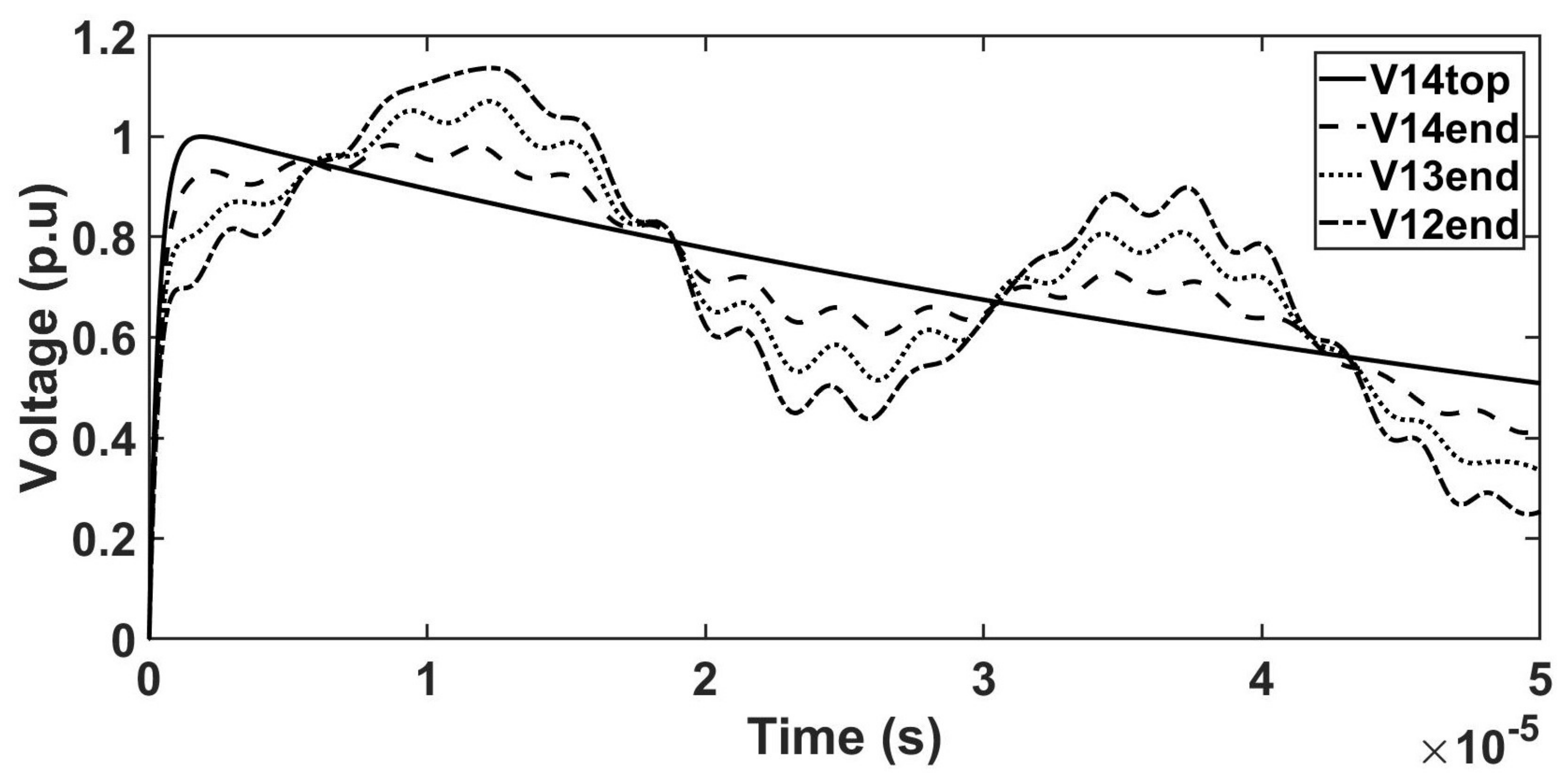
4.1.3. Case 3: Surge Voltage Distribution for the Transformer Model with Shield Placement between Layer 14 and 13 and between Layer 13 and 12
4.1.4. Case 4: Surge Voltage Distribution for the Transformer Model with Shield Placement between HV and LV Windings
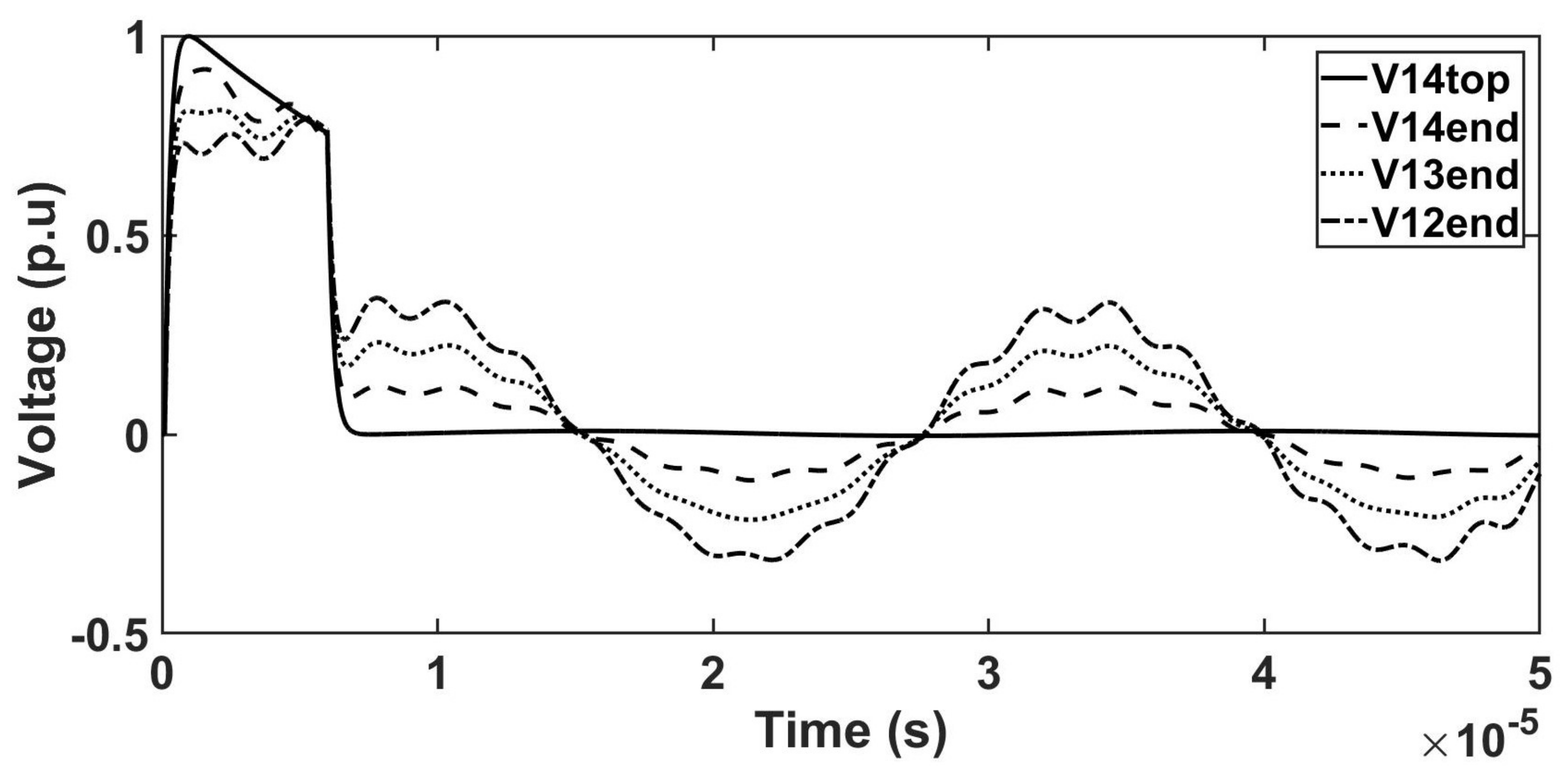
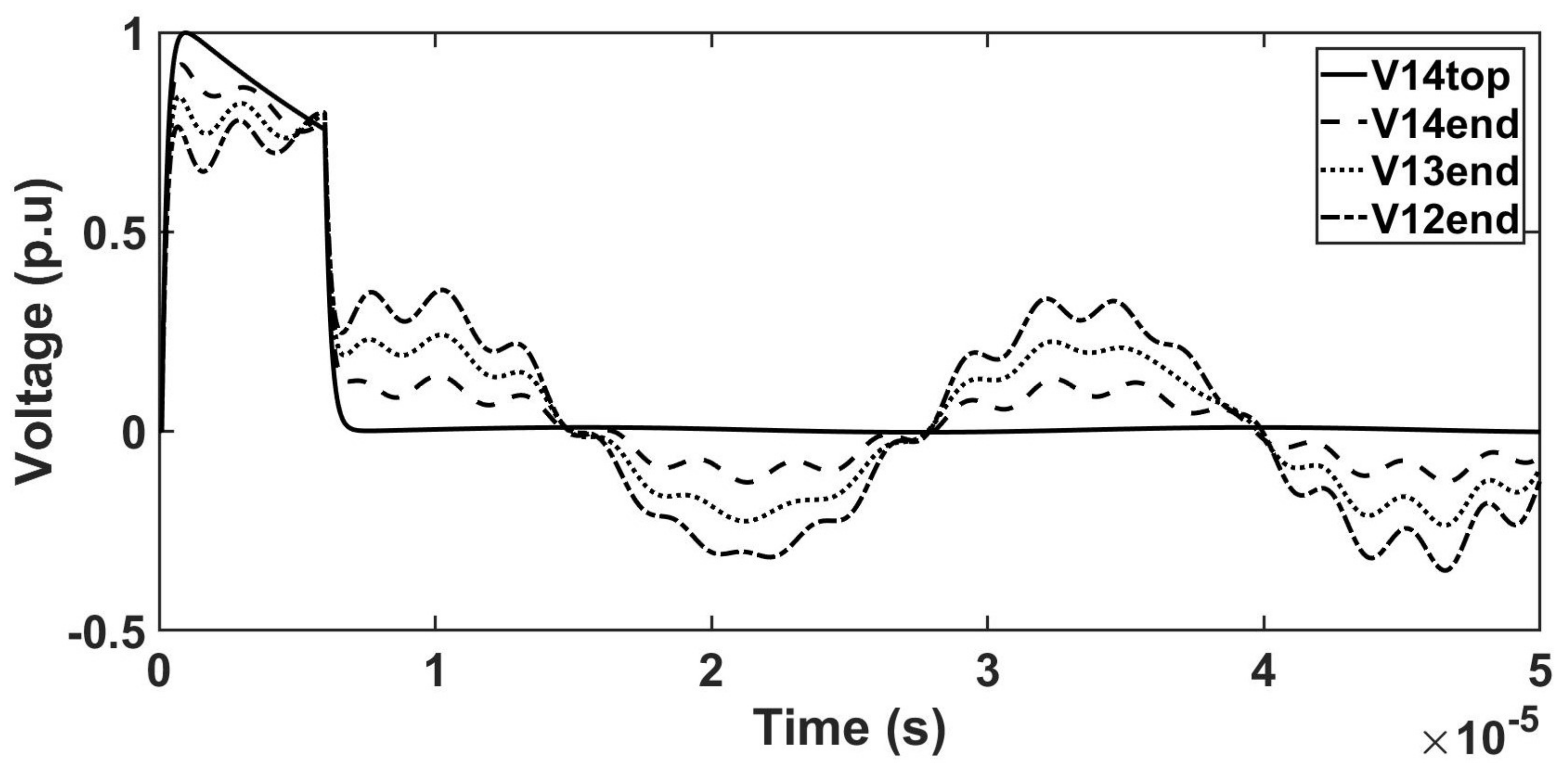
4.2. Surge Voltage Distribution under Chopped Lightning Impulse
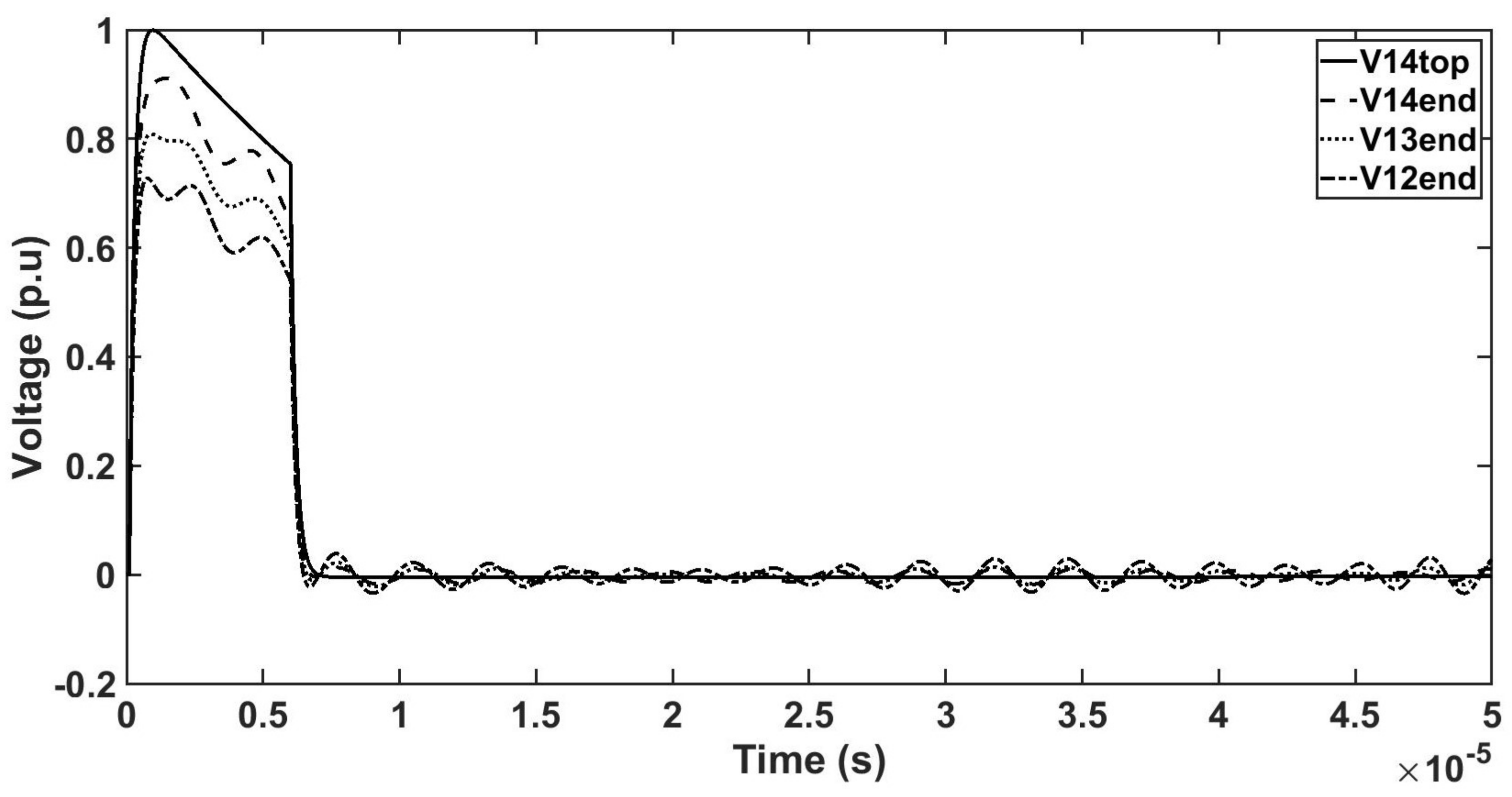
4.2.1. Case 1: Surge Voltage Distribution for the Transformer Model with Shield Placement between Layer 14 and Layer 13
4.2.2. Case 2: Surge Voltage Distribution for the Transformer Model with Grounded Shield Placement between Layer 14 and Layer 13
4.2.3. Case 3: Surge Voltage Distribution for the Transformer Model with Shield Placement between Layer 14 and Layer 13 and between Layer 13 and Layer 12
4.2.4. Case 4: Surge Voltage Distribution for the Transformer Model with Shield Placement between HV and LV Windings
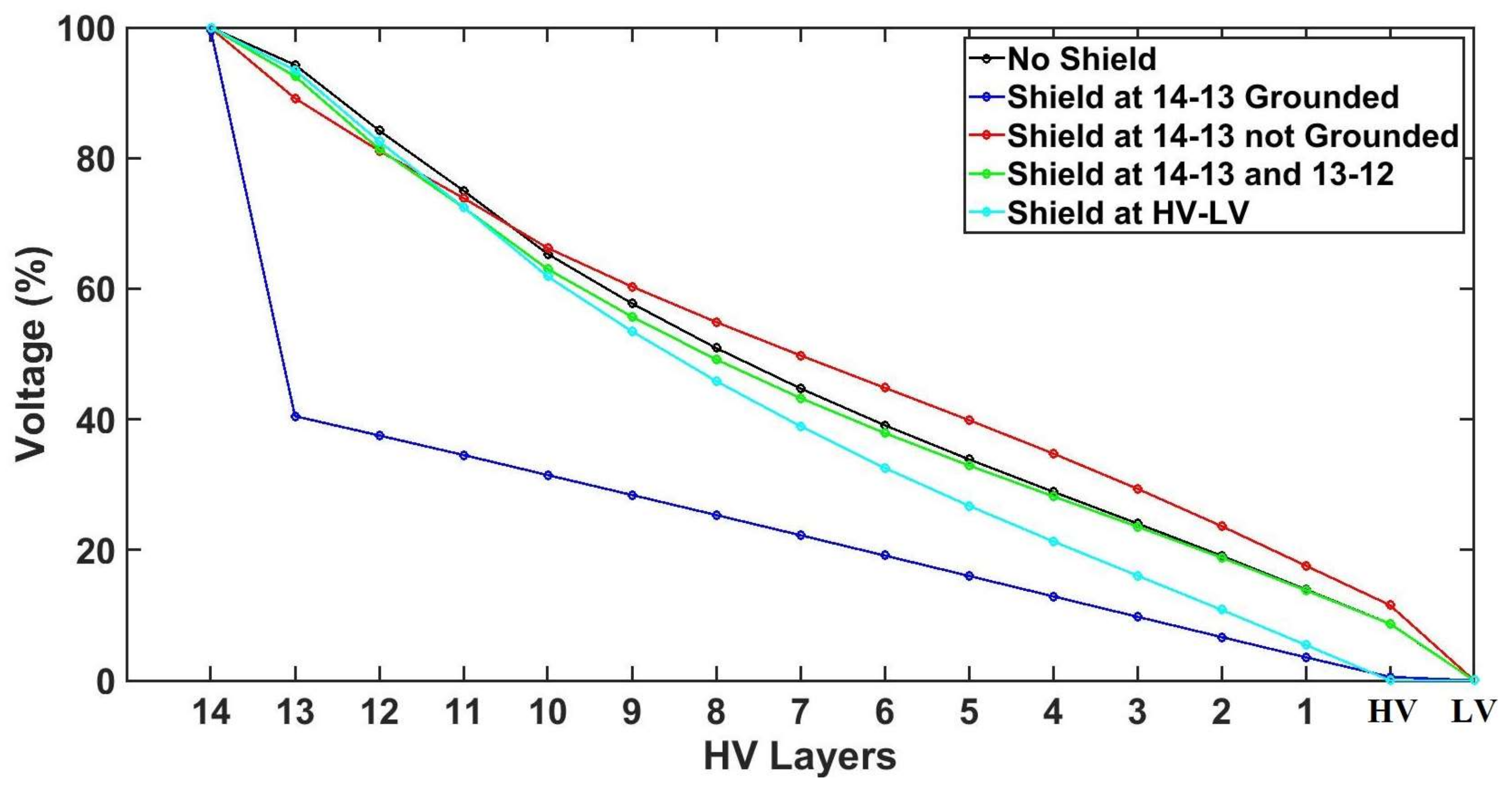
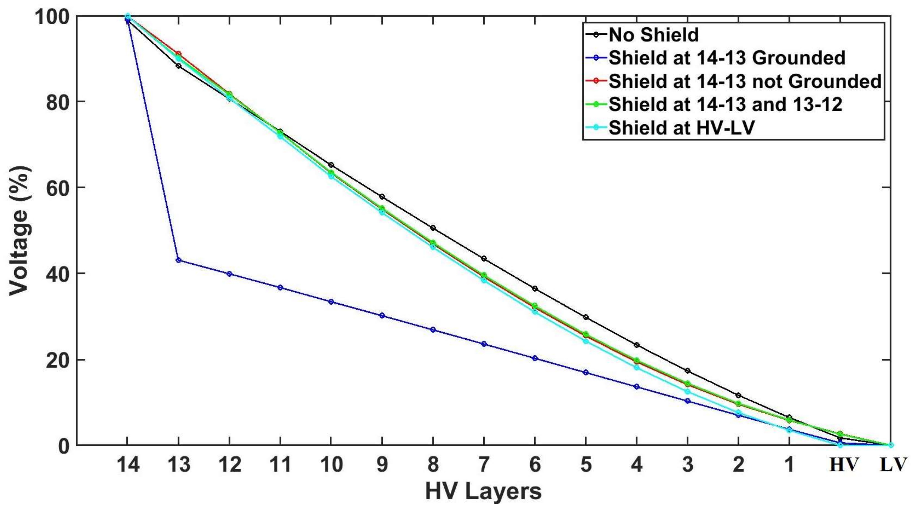
4.3. Discussion on the Effect of Shield Placements on the Initial Surge Voltage Distribution
5. Conclusions
Author Contributions
Funding
Acknowledgments
Conflicts of Interest
References
- IEEE Std C57.98-2011 (Revision of IEEE Std C57.98-1993)—IEEE Guide for Transformer Impulse Tests; IEEE Power and Energy Society: Park Avenue, NY, USA, 2012.
- IEEE Std C57.12.00-2010 (Revision of IEEE Std C57.12.00-2006)—IEEE Standard for General Requirements for Liquid-Immersed Distribution, Power, and Regulating Transformers; IEEE Power and Energy Society: Park Avenue, NY, USA, 2010.
- IEC 60076-4 (2002)—Part 4: Guide to the Lightning Impulse & Switching Impulse Testing—Power Transformers and Reactors; IEC Central Office 3, rue de Varembé, CH-1211: Geneva, Switzerland, 2002.
- IEC 60076-3 (2013) Power Transformers—Part 3: Insulation Levels, Dielectric Tests and External Clearances in Air; IEC Central Office 3, rue de Varembé, CH-1211: Geneva, Switzerland, 2013.
- Alfuhaid, A.S. Frequency characteristics of single-phase two-winding transformers using distributed-parameter modelling. IEEE Trans. Power Deliv. 2001, 16, 637–642. [Google Scholar] [CrossRef]
- Jayaram, S.; Chandrasekharaiah, H.S. Influence of secondary windings terminal conditions on impulse distribution in transformer windings. Electr. Mach. Power Syst. 1993, 21, 183–198. [Google Scholar] [CrossRef]
- Greenwood, A. Electrical Transients in Power Systems; Wiley-Interscience: New York, NY, USA, 1991. [Google Scholar]
- Popov, M.; Van der Sluis, L.; Paap, G.C.; De Herdt, H. Computation of very fast transient overvoltages in transformer windings. IEEE Trans. Power Deliv. 2003, 18, 1268–1274. [Google Scholar] [CrossRef]
- Lopez-Roldan, J.; De Herdt, H.; Declercq, J.; Sels, T.; Van Dommelen, D.; Popov, M.; Van Der Sluis, L. Analysis, Simulation and Testing of Transformer Insulation Failures Related to Switching Transients Overvolages; CIGRE: Paris, France, 2002; pp. 12–116. [Google Scholar]
- Theocharis, A.; Popov, M.; Seibold, R.; Voss, S.; Eiselt, M. Analysis of switching effects of vacuum circuit breaker on dry-type foil-winding transformers validated by experiments. IEEE Trans. Power Deliv. 2015, 30, 351–359. [Google Scholar] [CrossRef]
- Popov, M. General approach for accurate resonance analysis in transformer windings. Electr. Power Syst. Res. 2018, 161, 45–51. [Google Scholar] [CrossRef]
- Smajic, J.; Steinmatz, T.; Rüegg, M.; Tanasic, Z.; Obrist, R.; Tepper, J.; Weber, B.; Carlen, M. Simulation and Measurement of Lightning-Impulse Voltage Distributions Over Transformer Windings. IEEE Trans. Magn. 2014, 50, 553–556. [Google Scholar] [CrossRef]
- Zupan, T.; Trkulja, B.; Obrist, R.; Franz, T.; Cranganu-Cretu, B.; Smajic, J. Transformer Windings’ RLC Parameters Calculation and Lightning Impulse Voltage Distribution Simulation. IEEE Trans. Magn. 2016, 52, 2–5. [Google Scholar] [CrossRef]
- Gustavsen, B.; Brede, A.P.; Tande, J.O. Multivariate analysis of transformer resonant overvoltages in power stations. IEEE Trans. Power Deliv. 2011, 26, 2563–2572. [Google Scholar] [CrossRef]
- Hori, M.; Nishioka, M.; Ikeda, Y.; Noguchi, K.; Kajimura, K.; Motoyama, H.; Kawamura, T. Internal winding failure due to resonance overvoltage in distribution transformer caused by winter lightning. IEEE Trans. Power Deliv. 2006, 21, 1600–1606. [Google Scholar] [CrossRef]
- Bagheri, M.; Hekmati, A.; Heidarzadeh, R.; Naderi, M.S. Impulse voltage distribution in intershield disk winding VS interleaved and continuous disk winding in power transformer. In Proceedings of the PECon 2008—2008 IEEE 2nd International Power and Energy Conference, Johor Bahru, Malaysia, 1–3 December 2008; pp. 387–392. [Google Scholar]
- De Lima, P.A.P.; Cabral, S.H.L. A comparative analysis of performance of well-known methods for conforming distribution of impulsive voltage along regulating winding. In Proceedings of the 2013 IEEE Electrical Insulation Conference (EIC), Ottawa, ON, Canada, 2–5 June 2013; pp. 168–172. [Google Scholar]
- Adamczyk, B.; Florkowski, M.; Swiatkowski, M. Effect of shielding on surge overvoltages in multilayer type windings of power transformer. IEEE Trans. Dielectr. Electr. Insul. 2016, 23, 1627–1635. [Google Scholar] [CrossRef]
- Bagheri, M.; Phung, B.T.; Naderi, M.S. Impulse voltage distribution and frequency response of intershield windings. IEEE Electr. Insul. Mag. 2016, 32, 32–40. [Google Scholar] [CrossRef]
- McNutt, W.J. Transient voltage distribution improving line shield for layer wound power transformer. U.S. Patent No. 4,153,891, 8 May 1979. [Google Scholar]
- Khanali, M.; Jayaram, S.H. Effectiveness of electrostatic shielding in suppressing the impact of fast transients on transformer insulation. In Proceedings of the 2015 IEEE Conference on Electrical Insulation and Dielectric Phenomena (CEIDP), Ann Arbor, MI, USA, 18–21 October 2015; pp. 652–655. [Google Scholar]
- Wang, Z.; Li, J.; Sofian, D.M. Interpretation of transformer FRA responses—Part I: Influence of winding structure. IEEE Trans. Power Deliv. 2009, 24, 703–710. [Google Scholar] [CrossRef]
- Bagheri, M.; Vakilian, M.; Hekmati, A.; Heidarzadeh, R. Influence of electrostatic shielding of disc winding on increasing the series capacitance in transformer. In Proceedings of the 2007 IEEE Lausanne Power Tech, Lausanne, Switzerland, 1–5 July 2007; pp. 1780–1784. [Google Scholar]
- Pramanik, S.; Satish, L. Localisation of discrete change in a transformer winding: A network-function-loci approach. IET Electr. Power Appl. 2011, 5, 540–548. [Google Scholar] [CrossRef]
- Ragavan, K.; Satish, L. Localization of changes in a model winding based on terminal measurements: Experimental study. IEEE Trans. Power Deliv. 2007, 22, 1557–1565. [Google Scholar] [CrossRef]
- Wijayapala, W.D.A.S.; Karunananda, H.S.C. Mitigation of lightning surge stresses in the high voltage windings of distribution transformers by introducing an electrostatic shield. Eng. J. Inst. Eng. Sri Lanka 2015, 48.3, 1–11. [Google Scholar] [CrossRef]
- Verma, V.K. Practical Simulation and Modelling of Lightning Impulse Voltage Generator Using Marx Circuit; NITRKL: Odisha, India, 2014. [Google Scholar]
- Schon, K. Characterisation and Generation of High Impulse Voltages and Currents. In High Impulse Voltage and Current Measurement Techniques; Springer: Heidelberg, Germany, 2013; pp. 5–38. [Google Scholar]
- IEEE Std. C57.98-1994—IEEE Guide for Transformer Impulse Tests; Transformers Committee of the IEEE Power & Energy Society, IEEE: Park Avenue, NY, USA, 1994; pp. 1–59.
- Wheeler, H.A. Simple inductance formulas for radio coils. Proc. Inst. Radio Eng. 1928, 16, 1398–1400. [Google Scholar] [CrossRef]
- Wilcox, D.J.; Hurley, W.G.; Conlon, M. Calculation of self and mutual impedances between sections of transformer windings. IEE Proc. C Gener. Transm. Distrib. 1989, 136, 308–314. [Google Scholar] [CrossRef]
- Azimi, P.; Golnabi, H. Precise formulation of electrical capacitance for a cylindrical capacitive sensor. J. Appl. Sci. 2009, 9, 1556–1561. [Google Scholar] [CrossRef]
- Cylindrical Capacitor—phys.uri.edu. Available online: http://www.phys.uri.edu/gerhard/PHY204/tsl105.pdf (accessed on 10 October 2018).
- Hasthanayake, L.S. Distribution Transformer Model for Disribution Transformer Model for Transient Studies. M.Sc Thesis, University of Moratuwa, Moratuwa, Sri Lanka, 2014. [Google Scholar]
- Bjerkan, E. High frequency modeling of power transformers—Stresses and Diagnostics. Ph.D. Thesis, NTNU Norwegian University of Science and Technology, Trondheim, Norway, 2005. [Google Scholar]
- Rahimpour, E.; Christian, J.; Feser, K. Transfer function method to diagnose axial displacement and radial deformation of transformer windings. IEEE Trans. Power Deliv. 2009, 24, 730–739. [Google Scholar]
- Noda, T.; Nakamoto, H.; Yokoyama, S. Accurate modeling of core-type distribution transformers for electromagnetic transient studies. IEEE Trans. Power Deliv. 2002, 17, 969–976. [Google Scholar] [CrossRef]
- Bhuyan, M.; Chatterjee, S. Non Linear Voltage Distribution in Windings of Power Transformer. Int. J. Eng. Res. Technol. IJERT 2012, 1, 1–5. [Google Scholar]
- De, A.; Debnath, D.; Chakrabarti, A. A study on the impact of low-amplitude oscillatory switching transients on grid connected EHV transformer windings in a longitudinal power supply system. IEEE Trans. Power Deliv. 2009, 24, 679–686. [Google Scholar] [CrossRef]
- Florkowski, M.; Furgal, J.; Kuniewski, M.; Pajak, P. Comparison of transformer winding responses to standard lightning impulses and operational overvoltages. IEEE Trans. Dielectr. Electr. Insul. 2018, 25, 965–974. [Google Scholar] [CrossRef]
- De Oliveira Quevedo, J.; Cazakevicius, F.E.; Beltrame, R.C.; Marchesan, T.B.; Michels, L.; Rech, C.; Schuch, L. Analysis and design of an electronic on-load tap changer distribution transformer for automatic voltage regulation. IEEE Trans. Ind. Electron. 2017, 64, 883–894. [Google Scholar] [CrossRef]
- Stein, G.M. A study of the initial surge distribution in concentric transformer windings. IEEE Trans. Power Appar. Syst. 1964, 83, 877–893. [Google Scholar] [CrossRef]
- Gauper, H.A., Jr.; Walden, J.P. Electromagnetically Shielded Electrical Power Supply with Reduced Common Mode Electromagnetic Interference Output. US Patent 3963975A, 5 March 1976. [Google Scholar]
- Wang, S.; Zhang, H.; Wang, S.; Li, H.; Yuan, D. Cumulative Deformation Analysis for Transformer Winding Under Short-Circuit Fault Using Magnetic—Structural Coupling Model. IEEE Trans. Appl. Supercond. 2016, 26, 1–5. [Google Scholar] [CrossRef]
- Bjerkan, E.; Høidalen, H.K. High frequency FEM-based power transformer modeling: Investigation of internal stresses due to network-initiated overvoltages. Electr. Power Syst. Res. 2007, 77, 1483–1489. [Google Scholar] [CrossRef]


| Parameters | Values |
|---|---|
| Rch | 18 KΩ |
| C1 | 10 µF |
| Cl | 0.5 µF |
| Rf | 0.84 Ω |
| Rt | 5.96 Ω |
| Parameters | Values |
|---|---|
| Rch | 18 KΩ |
| Cin | 0.05 µF |
| CL | 10 nF |
| Rf | 333.33 Ω |
| Rt | 20 Ω |
| Parameters | Values |
|---|---|
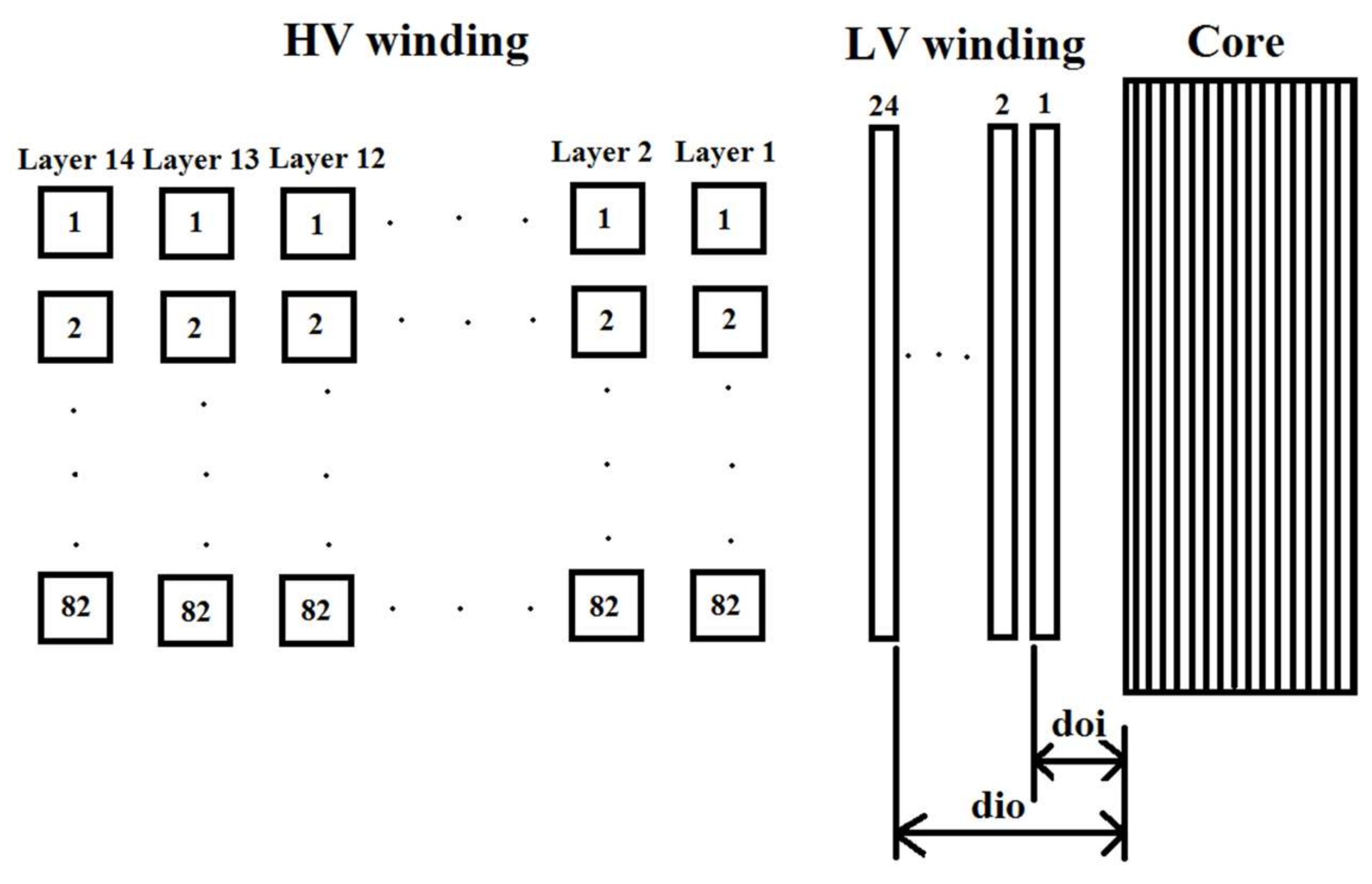
| Number of turns | 82 |
| Number of layers | 14 |
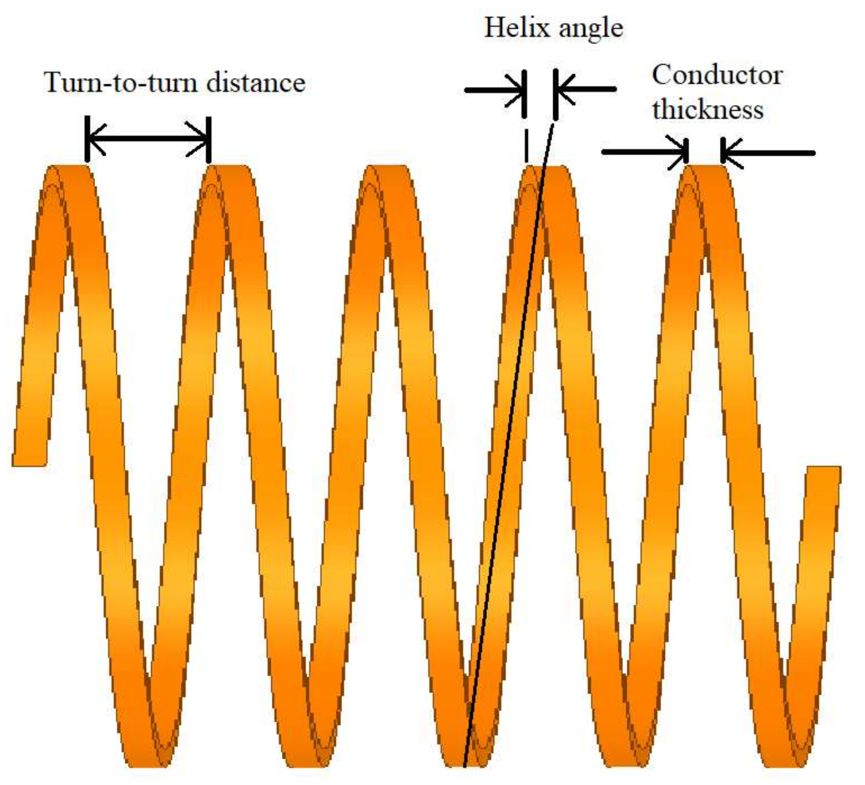
| Conductor/turn thickness | 3.15 mm |
| Insulation thickness between layers | 0.17 mm |
| Insulation thickness between turns | 0.17 mm |
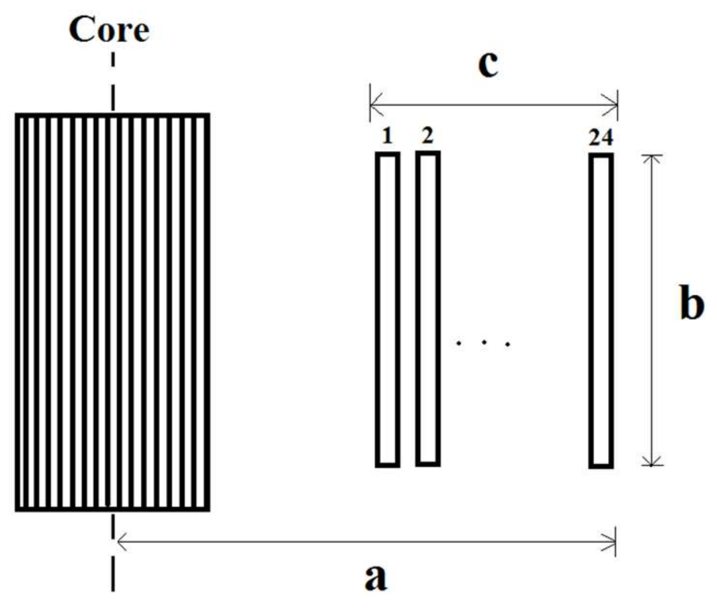
| Height of HV winding (including allowance) | 279.00 mm |
| Insulation between HV-LV windings | 4.03 mm |
| Distance from centre of core to end of HV winding | 96.65 mm |
| Distance from centre of the core to end of HV winding | 145.95 mm |
| Parameters | Values |
|---|---|
| Height of LV winding | 290 mm |
| Number of layers | 24 |
| Diameter of the core | 125 mm |
| Insulation between core and LV winding | 3.13 mm |
| Distance from core to LV winding | 65.63 mm |
| Conductor thickness of each layer | 1 mm |
| Insulation thickness between LV layers | 0.13 mm |
| Distance between core and end of LV layers | 92.96 mm |
| Internal width of the tank | 383.15 mm |
| Relative permittivity, | 3.3 |
| Layers | R (Ω) | L (µH) | Cll (pF) |
|---|---|---|---|
| 14 | 1.7637 | 1349 | 159.65 |
| 13 | 1.7231 | 1295 | 155.93 |
| 12 | 1.6825 | 1246 | 152.22 |
| 11 | 1.6420 | 1297 | 148.51 |
| 10 | 1.6014 | 1146 | 144.80 |
| 09 | 1.5609 | 1097 | 141.09 |
| 08 | 1.5203 | 1048 | 137.37 |
| 07 | 1.4798 | 1001 | 133.66 |
| 06 | 1.4392 | 954 | 129.95 |
| 05 | 1.3986 | 908 | 126.24 |
| 04 | 1.3581 | 863 | 122.53 |
| 03 | 1.3175 | 818 | 118.82 |
| 02 | 1.2770 | 775 | 115.11 |
| 01 | 1.2364 | 732 | - |
| Parameters | Values |
|---|---|
| Cgt′ | 11.805 pF |
| CHV-LV | 1033.7 pF |
| Cresultant | 1396.1 pF |
| LLV | 0.059 µH |
| RLV | 86.6784 Ω |
| Parameters | Values |
|---|---|
| C14shield | 394.65 pF |
| Cshield13 | 385.81 pF |
| L14 | 1350 µH |
| R14 | 1.7646 Ω |
| Parameters | Values |
|---|---|
| C14shield | 394.86 pF |
| Cshield13 | 386.02 pF |
| C13shield | 385.58 pF |
| Cshield12 | 376.74 pF |
| L14 | 1351 µH |
| L13 | 1298 µH |
| R14 | 1.7655 Ω |
| R13 | 1.7240 Ω |
| Layers | R (Ω) | L (µH) | Cll (pF) |
|---|---|---|---|
| 14 | 1.7646 | 1350 | 159.73 |
| 13 | 1.7270 | 1298 | 156.02 |
| 12 | 1.6835 | 1247 | 152.31 |
| 11 | 1.6429 | 1298 | 148.59 |
| 10 | 1.6023 | 1147 | 144.88 |
| 09 | 1.5618 | 1098 | 141.17 |
| 08 | 1.5212 | 1049 | 137.46 |
| 07 | 1.4807 | 1011 | 133.75 |
| 06 | 1.4401 | 955 | 130.04 |
| 05 | 1.3996 | 909 | 126.32 |
| 04 | 1.3590 | 864 | 122.61 |
| 03 | 1.3184 | 819 | 118.90 |
| 02 | 1.2779 | 776 | 115.19 |
| 01 | 1.2373 | 733 | - |
| Parameters | Values |
|---|---|
| Cgt′ | 11.805 pF |
| CHV-LV | 1695.2 nF |
| Cresultant | 1396.1 pF |
| LLV | 0.059 µH |
| RLV | 86.6784 Ω |
© 2019 by the authors. Licensee MDPI, Basel, Switzerland. This article is an open access article distributed under the terms and conditions of the Creative Commons Attribution (CC BY) license (http://creativecommons.org/licenses/by/4.0/).
Share and Cite
Srikanta Murthy, A.; Azis, N.; Mohd Yousof, M.F.; Jasni, J.; Othman, M.L.; Talib, M.A.; Das, B.P. Investigation on the Resonant Oscillations in an 11 kV Distribution Transformer under Standard and Chopped Lightning Impulse Overvoltages with Different Shield Placement Configurations. Energies 2019, 12, 1466. https://doi.org/10.3390/en12081466
Srikanta Murthy A, Azis N, Mohd Yousof MF, Jasni J, Othman ML, Talib MA, Das BP. Investigation on the Resonant Oscillations in an 11 kV Distribution Transformer under Standard and Chopped Lightning Impulse Overvoltages with Different Shield Placement Configurations. Energies. 2019; 12(8):1466. https://doi.org/10.3390/en12081466
Chicago/Turabian StyleSrikanta Murthy, Avinash, Norhafiz Azis, Mohd Fairouz Mohd Yousof, Jasronita Jasni, Mohammad Lutfi Othman, Mohd Aizam Talib, and Bhaba Priyo Das. 2019. "Investigation on the Resonant Oscillations in an 11 kV Distribution Transformer under Standard and Chopped Lightning Impulse Overvoltages with Different Shield Placement Configurations" Energies 12, no. 8: 1466. https://doi.org/10.3390/en12081466
APA StyleSrikanta Murthy, A., Azis, N., Mohd Yousof, M. F., Jasni, J., Othman, M. L., Talib, M. A., & Das, B. P. (2019). Investigation on the Resonant Oscillations in an 11 kV Distribution Transformer under Standard and Chopped Lightning Impulse Overvoltages with Different Shield Placement Configurations. Energies, 12(8), 1466. https://doi.org/10.3390/en12081466