Article

FPGA Based Real-Time Emulation System for Power Electronics Converters

Faculty of Electrical Engineering and Computer Science, University of Maribor, Koroška cesta 46, 2000 Maribor, Slovenia
*
Author to whom correspondence should be addressed.
Energies 2019, 12(6), 969; https://doi.org/10.3390/en12060969
Submission received: 29 January 2019 / Revised: 20 February 2019 / Accepted: 10 March 2019 / Published: 13 March 2019
(This article belongs to the Section F: Electrical Engineering)

Abstract

:
This paper deals with an emulation system for Power Electronics Converters (PEC). The emulation of PECs is performed on a Field-Programmable Gate Array (FPGA) capable of hard real-time operation. To obtain such a system, the converter operation is described using a differential equations-based model designed with the graph theory. Differential equation coefficients are changed according to the type of converter and pulse-width modulation (PWM) signals. The tie-set and incidence matrix approach for the converter modelling is performed to describe the converter operation in a general way. Such approach enables that any type of PECs can be described appropriately. The emulator was verified experimentally by synchronous operation with a real DC-AC converter built for this purposes.

1. Introduction

In recent years, demand for utilization of power electronic converters in industrial, commercial and household applications has increased significantly. It is critical for engineers to design these converters very quickly. Considering the time constraints on engineers, it is not surprising that rapid prototyping tools, different Hardware-in-the-Loop (HiL) systems and fault diagnosis techniques have become the key issue in Power Electronics System (PES) applications. For these applications, the modelling techniques process enables faster developing of the PESs. Off-line simulation using different tools is used widely to predict the behaviour of PESs in a time domain. Some ideas of simulation are exploited to some extent for real-time application as estimators and observers in different control processes.
HiL emulation techniques are used extensively in the control of electrical motors and generators designs as reported in [1,2,3,4,5], where the authors used the HiL emulator approach for rapid prototyping issues and studying fault tolerant operation of the observing systems. The research in [1] deals with the design and application of a new ultra-high speed real-time emulation platform for HiL testing and design of high-power PESs. The real-time HiL emulation is performed with a reconfigurable, heterogeneous, multi-core processor architecture that emulates power electronics and includes a circuit compiler that translates graphic system models into processor executable machine code. The authors of [2] developed a synchronous generator emulator by using a three-phase voltage source converter for transmission level power system testing. The research is concentrated to study the different interface algorithms in order to select the ideal voltage type transformer model by considering accuracy and stability. By means of decreasing the emulation error, a closed-loop voltage control is proposed with current feed-forward. The usage of the emulation system for study of the operation of DC-DC converters in a fuel-cell vehicle power-train application is studied in [3]. The bidirectional buck-boost type DC-DC converter is considered as a basic element, which is used as a device under test, and the rest of the system is emulated. Fault tolerant methods are described in [4,5]. Experimental tools for the development of fault-tolerant machines designed for aerospace motor drives are described in [4], where the authors studied safety critical systems that should be able to overcome hardware or software faults and, therefore, need to be fault tolerant. For safety purposes, the multi-phase machine is chosen to improve the fault-tolerance. The fault tolerant principle for a five-phase permanent-magnet motor operated with an appropriate PEC is described in [5]. The authors improved the motor operation under the open-circuit fault condition and proposed a new, remedial field-oriented control strategy. A review of literature on HiL systems yields several existing methods based on process modelling for the given systems [6,7,8,9,10]. These methods start by process modelling mainly for the high power systems, where it is suitable to study all modes of operation by developed models to avoid costs for real-time experimentation.
The complex power-transmission networks are usually modelled by using graph-theory because of its complexity. To study different operation modes, the incidence matrix approach is recognised as the most useful one. The usage of the network graph theory in this role is reviewed in [11,12,13,14,15,16,17]. In [11], the authors demonstrated the consequence of the calculated nodal voltages and branch currents to the eigenvalues and eigenvectors of the Laplacian matrix, which describes the connectivity of the electrical network. The authors of [12] exploited the benefits of systematic analyses by using the complex network theory in order to study the impact of the wind power system to the power grid. The reason why grid-connected wind power should be mitigated is interpreted based on the complex network theory. In the work presented in [13], the authors demonstrated how a simple model of an AC network for three-phase unbalanced power flow with embedded transformers can be obtained, conjugating the use of a complex vector based model in a stationary reference frame and the node incidence matrix based formulation. Zhang [14] proposed a numerical method, which identifies all the single and double edges of the network cut-sets in order to address these vulnerabilities. The described method is based on the factorization of reduced incidence matrix. Reliability Evaluation of the power system also relies on the fault incidence matrix approach. The authors of [15] proposed such an algorithm. Saleh [16] provided a review of the research conducted on complex network analysis in electric power systems. This work presents the finding of the optimal locations for micro-grids in electric distribution systems utilising complex network analysis. In [17], the authors researched the energy flow, material flow and information flow, considering the inherent dynamism and uncertainty of material, energy and information flows, by using the static and dynamic incidence matrices. The modelling approaches for different PECs are described in [18,19], where the authors described the connections of algebraic graph theory, the design and analysis of electric circuits for different network systems.
The emulation of the physical systems is recognised as a modern approach for rapid prototyping of different PESs in order to develop fast and cheap motor drives for different applications. However, all the above described approaches extract the power converter system from the emulators, and the PES is considered as HiL and the rest of the system is emulated due to the cost. The work described here deals with a software/hardware FPGA platform for emulation and verification of PES. The DC-AC converter is chosen to verify the thesis that any PEC can be described by mathematical models, which enables the detailed real-time emulation. The verification system consists of a real DC-AC converter and emulator, which is operating inside the FPGA in real-time, as shown in Figure 1. The paper is organised into five sections. The principle of system operation, method for developing the differential equations for a DC-AC converter model, and features the necessary mathematical background for modelling purposes are described in Section 2. The tie-set and incidence-matrix approach is also introduced for PEC modelling. Section 3 deals with the hardware system necessary in order to solve the developed differential equations by using the FPGA platform. The verification of the method is described in Section 4 as a description and discussion of the obtained experimental results. The main contribution of the paper is the proof of the thesis that it is possible to perform the emulation in real-time, synchronised with the operation of a real DC-AC converter. In general, by using the incidence matrix approach, any PEC can be described. Finally, the conclusion and contributions of this paper are outlined in Section 5 together with suggestions for future research topics.

2. Modelling Method Description

To develop the PEC model, the network topology based on Kirchhoff’s laws can be used. The network topology analysis is based on graphical representation of the electric circuits. This method is useful for analysing the complex electric circuits by converting them into network graphs. More precisely, the theory of network topology analyses can be found in [20]. The network representing the single-phase DC-AC converter shown in Figure 2a was chosen for describing the modelling method.

2.1. Basic Terminology for the Graph Theory

Any electric circuit or network (Figure 2a) can be transformed into a so-called equivalent graph, as shown in Figure 2b. Thus, an equivalent graph is obtained by replacing the passive elements (R, L, C, diodes or transistors) and voltage sources by short circuits, and the current sources by open circuits. A network graph could be connected, unconnected, directed or undirected. A graph is said to be directed (or oriented) when all the nodes and branches are numbered, and direction is assigned to the branches by arrow. The branch represents the line segment, indicated by Arabic numbers, that connects two nodes indicated by Arabic numbers in the circle. In electric circuits, the arrows can indicate the direction of current flow in each branch. For modelling purposes, the connected and directed graph is considered and the definitions of two sub-graphs, so-called tree and co-tree, need to be explained.
  • Tree is a connected sub-graph of a given graph, where branches only connect graph nodes. Tree is shown in Figure 2b indicated by bold lines. The branches of a tree are called twigs. A tree consists of only branches that do not form loops. The number of tree branches ( b T ) that form a graph tree can be calculated:
    b T = n 1
    where n represents the number of nodes.
  • Co-Tree is a sub-graph, which is formed with the branches that are removed while forming a tree. It is indicated in Figure 2b by dashed lines. If branches from the co-tree are connected to the tree, loops are formed. Hence, it is called a complement of a tree. For every tree, there will be a corresponding co-tree, and its branches are called links or chords.
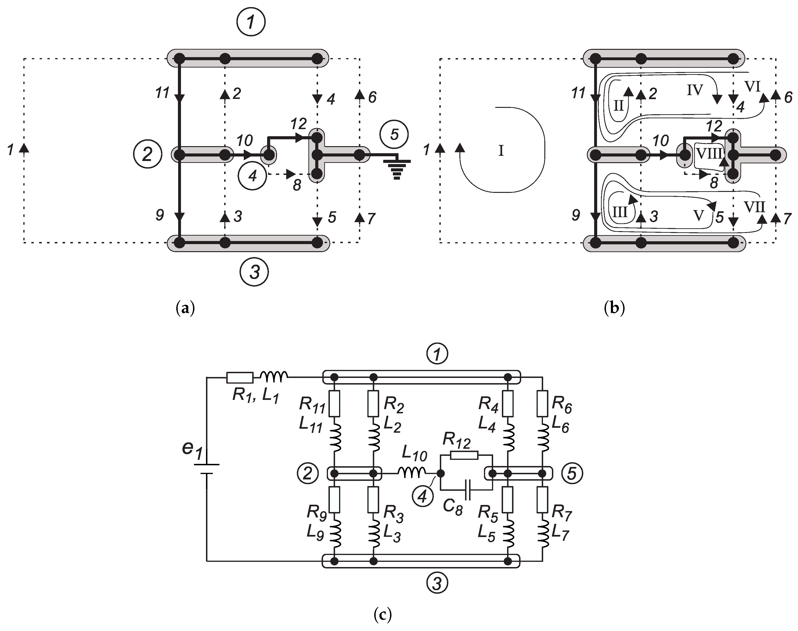
  • Incidence matrix is description of any oriented graph in a compact matrix form. The incident matrix translates the graphical data of a network into algebraic form. For a graph with n nodes and b branches, the complete incidence matrix A i is an n × b matrix with elements defined by:
    a j i = 1 ; if branch i leaves node j 1 ; if branch i enters node j 0 ; if branch i is not incident with node j
    Using Kirchhoff’s Current Law (KCL), the rules can be obtained for an incidence matrix. For the chosen circuit graph shown in Figure 2a, it follows:
    i 1 i 2 + i 4 i 6 + i 11 = 0 i 2 i 3 + i 9 + i 10 i 11 = 0 i 1 + i 3 i 5 + i 7 i 9 = 0 i 8 i 10 + i 12 = 0 i 4 + i 5 + i 6 i 7 i 8 i 12 = 0
    where i 1 i 12 represent the branch currents, which are depicted in Figure 3a. Equation (2) can be expressed in the matrix form as follows:
    n b 1 2 3 4 5 6 7 8 9 10 11 12 1 2 3 4 5 1 1 0 1 0 1 0 0 0 0 1 0 0 1 1 0 0 0 0 0 1 1 1 0 1 0 1 0 1 0 1 0 1 0 0 0 0 0 0 0 0 0 0 1 0 1 0 1 0 0 0 1 1 1 1 1 0 0 0 1 A i i 1 i 2 i 3 i 4 i 5 i 6 i 7 i 8 i 9 i 10 i 11 i 12 i b = 0 0 0 0 0 0
    where A i represents the incidence matrix. If one complete row is removed from an incidence matrix, it results in a reduced incidence matrix, which is appropriate for further calculations. By choosing the node 5 as a reference node, and according to the graph shown in Figure 3a, the reduced incidence matrix is:
    1 2 3 4 1 1 0 1 0 1 0 0 0 0 1 0 0 1 1 0 0 0 0 0 1 1 1 0 1 0 1 0 1 0 1 0 1 0 0 0 0 0 0 0 0 0 0 1 0 1 0 1 A i 1 i 2 i 3 i 4 i 5 i 6 i 7 i 8 i 9 i 10 i 11 i 12 i b = 0 0 0 0 0
    and using the matrix notations, it follows:
    A i b = 0
    where A represents the reduced incidence matrix and i b is the branch current vector. Equation (5) also gives the maximum possible number of linearly-independent KCL equations for a connected circuit. The numbers of rows (N) in the reduced incidence matrix is:
    N = n 1
    where n is number of all graph nodes. To calculate the nodes voltages, Kirchhoff’s Voltage Law (KVL) can be used to connect branch and nodes voltages as follows:
    v 1 = V 1 + V 3 v 2 = V 1 + V 2 v 3 = V 2 + V 3 v 4 = V 1 v 5 = V 3 v 6 = V 1 v 7 = V 3 v 8 = V 4 v 9 = V 2 V 3 v 10 = V 2 V 4 v 11 = V 1 V 2 v 12 = V 4
    which leads to:
    v 1 v 2 v 3 v 4 v 5 v 6 v 7 v 8 v 9 v 10 v 11 v 12 v b = 1 0 1 0 1 1 0 0 0 1 1 0 1 0 0 0 0 0 1 0 1 0 0 0 0 0 1 0 0 0 0 1 0 1 1 0 0 1 0 1 1 1 0 0 0 0 0 1 A T V 1 V 2 V 3 V 4 V N
    and in the matrix form
    v b = A T V N
  • Tie-set matrix
    For a given tree of a graph, the addition of each link between any two nodes forms a loop called the fundamental loop. In a loop, there exists a closed path and a circulating current, which is called the link current. The fundamental loop formed by one link has a unique path in the tree joining the two nodes of the link. This loop is also called a f-loop or a tie-set. The current in any branch of a graph can be found by using link currents. Consider the connected graph shown in Figure 3a, which has five nodes and twelve branches. In general, the tree branches are chosen arbitrarily, and are indicated by a bold line, as shown in Figure 3a. The twigs of this tree are branches 9–12. The links corresponding to this tree are branches 1–8. Every link defines a fundamental loop of the network. The number of graph links (or f-loops) b can be calculated as follows:
    b = b n + 1
    Thus, for a given oriented graph (Figure 3), the next set of parameters are defined: the number of nodes ( n = 5 ), number of branches ( b = 12 ), number of tree branches or twigs ( b T = n 1 = 4 ), and number of link branches ( b = b n + 1 = 8 ). KVL can be applied to the f-loops to get a set of linearly independent equations. Consider Figure 3b, where there are eight fundamental loops i I i V I I I corresponding to the link branches 1–8, respectively. If v 1 , v 2 , . . . v 12 are the branch voltages, the KVL equations for the tree f-loops can be written as:
    v 1 + v 9 + v 11 = 0 v 2 + v 11 = 0 v 3 + v 9 = 0 v 4 v 10 v 11 v 12 = 0 v 5 v 9 + v 10 + v 12 = 0 v 6 + v 10 + v 11 + v 12 = 0 v 7 + v 9 v 10 + v 12 = 0 v 8 v 12 = 0
    and in matrix form, Equation (11) becomes:
    b b 1 2 3 4 5 6 7 8 9 10 11 12 I II III VI V VI VII VIII 1 0 0 0 0 0 0 0 1 0 1 0 0 1 0 0 0 0 0 0 0 0 1 0 0 0 1 0 0 0 0 0 1 0 0 0 0 0 0 1 0 0 0 0 0 1 1 1 0 0 0 0 1 0 0 0 1 1 0 1 0 0 0 0 0 1 0 0 0 1 1 1 0 0 0 0 0 0 1 0 1 1 0 1 0 0 0 0 0 0 0 1 0 0 0 1 B v 1 v 2 v 3 v 4 v 5 v 6 v 7 v 8 v 9 v 10 v 11 v 12 v b = 0 0 0 0 0 0 0 0 0
    or
    B v b = 0
    where B is a so-called tie-set matrix or fundamental loop matrix, and v b is a column vector of the branch voltages.
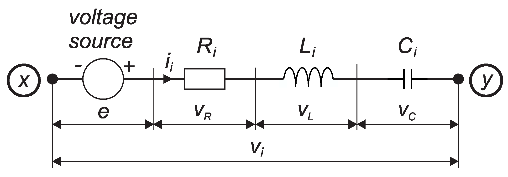
  • Tie-set matrix and branch currents
    Let i 1 , i 2 , . . . , i 12 be the branch currents with directions as shown in Figure 3a. Then, add the links in their proper places to the tree, as shown in Figure 3b. It can be seen that the loops currents are formed by the tree branches 9–12. There is a formation of link currents indicated in Figure 3b by Roman numbers i I , i I I , . . . , i V I I . By convention, the f-loops currents are given the same orientation as their defining links currents, i.e., the link current i I coincides with the branch current direction i 1 , the link current i I I coincides with the branch current direction i 2 , and so on until the link current i V I I coincides with the branch current direction i 7 , and, according to tree branches, the branches currents are combinations of f-loops currents. Thus, based on these assumptions, branches currents related with the loops currents can be expressed as:
    i 1 = i I i 2 = i I I i 3 = i I I I i 4 = i I V i 5 = i V i 6 = i V I i 7 = i V I I i 8 = i V I I I i 9 = i I + i I I I i V + i V I I i 10 = i I V + i V + i V I i V I I i 11 = i I + i I I i I V + i V I i 12 = i I V + i V + i V I i V I I i V I I I
    Equation (14) can be written in matrix form as:
    i 1 i 2 i 3 i 4 i 5 i 6 i 7 i 8 i 9 i 10 i 11 i 12 i b = 1 0 0 0 0 0 0 0 0 1 0 0 0 0 0 0 0 0 1 0 0 0 0 0 0 0 0 1 0 0 0 0 0 0 0 0 1 0 0 0 0 0 0 0 0 1 0 0 0 0 0 0 0 0 1 0 0 0 0 0 0 0 0 1 1 0 1 0 1 0 1 0 0 0 0 1 1 1 1 0 1 1 0 1 0 1 0 0 0 0 0 1 1 1 1 1 B T i I i I I i I I I i I V i V i V I i V I I i V I I I i
    which leads to:
    i b = B T i

2.2. General “Construction” of Circuit Differential Equations

The basic KVL and KCL used by the graph are explained above, which enables two different approaches for power converters modelling. In general, the node voltage or loop current calculation approach can be used.

Loop Current Differential Equations

According to the circuit and its graph, shown in Figure 2a,b, and to apply the above mentioned tie-set matrix developed facts, one branch can be extracted from the circuit. In general, between two arbitrary nodes x and y, there is a branch where the voltage source (e), the resistor (R), inductor (L) and the capacitor (C) can be present, as shown in Figure 4.
For every branches voltages in the circuit, the KVL gives:
v i = e i + R i i i + L i d i i d t + S i q i
where e i is the voltage source present in the branch, i i is the branch current, q i is the charge present in the branch, and R i , L i and S i ( S i = 1 / C i ) are branch resistance, inductance and elastance respectively (elastance S = 1 / C ). Using the known connection between capacitor charge and currents yields:
d q i d t = i i
where i = 1 , 2 , 3 , b . Thus, for every graph branch, it is possible to write down its own equation, as follows:
v 1 = e 1 + R 1 i 1 + L 1 d i 1 d t + S 1 q 1 v 2 = e 2 + R 2 i 2 + L 2 d i 2 d t + S 2 q 2 v b = e b + R b i b + L b d i b d t + S b q b
Equation (19) can be expressed in a matrix form as follows:
v b = e b + R b i b + L b d i b d t + S b q b d q b d t = i b
where
v b = v 1 v 2 v b , e b = e 1 e 2 e b , i b = i 1 i 2 i b , q b = q 1 q 2 q b ,
R b = R 1 0 0 0 R 2 0 0 0 R b , L b = L 1 0 0 0 L 2 0 0 0 L b , S n = S 1 0 0 0 S 2 0 0 0 S b
where v b represents the voltage vector with the elements v 1 , v 2 , . . . , v b ; e b represents the voltage sources vector with the components e 1 , e 2 , . . . , e b ; i b represents the current branch vector with the elements i 1 , i 2 , . . . i b ; q b represents the branch charges vector (i.e., capacitor voltages vector) with the components q 1 , q 2 , . . . , q b ; R b represents the resistance branch matrix with the elements R 1 , R 2 , . . . , R b ; L b represents the inductance branch matrix with the components L 1 , L 2 , . . . , L b ; and S b represents the elastance branch matrix with the elements S 1 , S 2 , . . . S b . The system in Equation (20) represents the voltage drop on every circuit branch. With the KVL applied, which means that every equation member must be multiplied on the left side by tie-set matrix B , Equation (20) is modified as follows:
Bv b = Be b + BR b i b + BL b d i b d t + B S b q b d q b d t = i b
According to Equation (13) term B v b = 0 , substituting Equation (16) into Equation (23), and considering that q b = B T q , yields:
0 = e + BR b B T i + BL b B T d i d t + B S b B T q d q d t = i
where e ( e = B e b ) represents the transformation of branch voltage sources into the loops. After rearranging Equation (24), it follows:
d i d t = L 1 e R i S q d q d t = i
where R = B R b B T , S = B S b B T and L = B L b B T .
The matrices R , S and L are called the loops matrices, and have the dimension × .
R = b 11 b 12 b 1 b b 21 b 22 b 2 b b 1 b 2 b b b R 1 0 0 0 R 2 0 0 0 0 0 0 0 0 0 0 0 R b b 11 b 21 b 1 b 12 b 22 b 2 b b 1 b b 2 b b b
L = b 11 b 12 b 1 b b 21 b 22 b 2 b b 1 b 2 b b b L 1 0 0 0 L 2 0 0 0 0 0 0 0 0 0 0 0 L b b 11 b 21 b 1 b 12 b 22 b 2 b b 1 b b 2 b b b
S = b 11 b 12 b 1 b b 21 b 22 b 2 b b 1 b 2 b b b S 1 0 0 0 S 2 0 0 0 0 0 0 0 0 0 0 0 S b b 11 b 21 b 1 b 12 b 22 b 2 b b 1 b b 2 b b b
The obtained system in Equation (25) describes the circuit by using the state variables, i.e., the inductor currents and capacitor voltages, and enables the modelling of the converter circuit.

2.3. Consideration of Circuit Loops Matrices

For converter emulation purposes, it is necessary to define the branches where the semiconductors switches and diodes are present. According to the DC-AC converter scheme (Figure 2a) and established graph (Figure 3a), the transistors are present in branches 4, 5, 9 and 11, and diodes in branches 2, 3, 6 and 7. For MOSFETs and diodes, the ON resistance and inductance are chosen to be R o n = 20 m Ω , L o n = 20 nH, and for OFF state R o f f = 100 k Ω , L o f f = 100 mH respectively. In this example, MOSFETs are used but there are also possibilities of other semiconductor switches (IGBT, GaN, SiC, etc.), where the correct equivalent resistances, inductances and applicable PWM technique should be used.

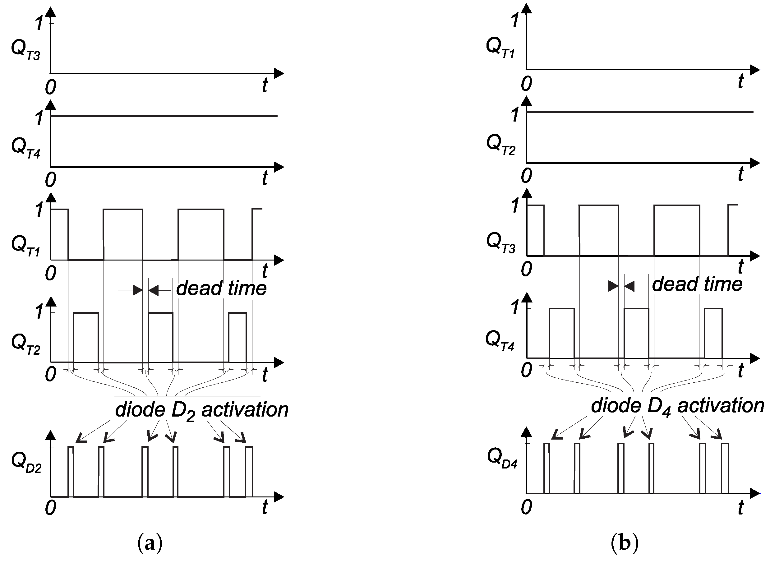
2.3.1. Control of Branches Containing Transistors

The emulation of switching the transistor is performed by changing the modelled equivalent resistance and inductance in the branches with semiconductors according to the used modulation signal and voltage polarity. Thus, by defining the branches with transistors, and by including the triggering pulses in order to select correct equivalent resistances R i ( R o n or R o f f ) and inductances L i ( L o n or L o f f ) in appropriate branches of Equations (26) and (27), respectively, the obtained loops matrices can be used for converter emulation. To control the emulation variables, it is necessary for the circuit loops matrices to be connected with pulse width modulation (PWM) signals [21].
Based on the chosen graph (Figure 3) and using Table 1, the appropriate R o n , L o n and R o f f , L o f f values should be used in the branches containing the transistors. To produce the three-level voltage on the converter output, the necessary gate signals are shown in Figure 5. When gate signals Q T 1 Q T 4 are equal to logic value 1, the matrices R b and L b contain R o n and L o n in appropriate branches, and, when these are equal to logic value 0, the matrices contain R o f f and L o f f in appropriate branches.

2.3.2. Control of Branches Containing Diodes

The emulation of switching the diodes is performed by changing the resistance and inductance in the branches with diodes according to the voltage polarity. To make the diode forward or reverse biased, the branch voltages where diodes are present can be evaluated by Equations (7) and (19) with the help of Equation (25). During the integration process (solving the differential equation system), it is necessary to calculate the exact voltage transient through zero, which is almost impossible. For simulation purposes, it is possible by introducing the iteration approach and changing the simulation step in order to obtain exactly the diode voltage transient-zero point [22], but for emulation purposes such approach is not appropriate. On the other hand, the exact time when diodes must be active is known by generated gate signals Q T 1 Q T 4 for transistors T 1 T 4 . To obtain the three-level output voltage between the nodes 2 and 5 , the dead-time intervals between transistors in the converter leg must be generated (first leg transistors T 1 and T 2 and second leg T 3 and T 4 ). During these intervals, the diodes must be activated, as shown in Figure 6a,b, respectively. The appropriate time sequences when diodes are active are shown in Figure 7a,b. Based on this, the decision table (Table 2) can be established, and the boolean logic function can be developed by using Karnaugh Maps minimization as follows:
Q D 2 = Q ¯ T 1 & Q ¯ T 2 Q D 4 = Q ¯ T 3 & Q ¯ T 1
where Q D 2 and Q D 4 represent the logic signals with values 1 or 0. They are controlling branches 3 and 7, where the diodes are present, by putting in the branches the values R o n , L o n or R o f f , L o f f . Thus, the diode states ON or OFF are controlled indirectly by the PWM generator, which is summarised in Table 3. Diodes D 1 and D 3 are not active in any of the possible states of the converter by applied modulation, which can be seen in Figure 6. That is why branches 2 and 6 always have the values R o f f and L o f f , respectively.
Some combinations of the gate signals should never appear (Table 2), and can be used for FPGA logic cells configuration error identification (for safety reasons). Thus, if any of these combinations appear, it can be decoded as an error, which is indicated in the last column of Table 2. Boolean logic function for modulation error is also developed by Karnaugh Maps as follows:
E r r o r = Q T 1 & Q T 2 O R Q T 3 & Q T 4 O R Q ¯ T 2 & Q T 3 O R Q T 1 & Q ¯ T 4
To evaluate the voltages appearing on the transistors placed in the branches 4, 5, 9 and 11 and the voltages appearing on the diodes in the branches 2, 3, 6 and 7, the following procedure should be carried out. Loops currents can be calculated using Equation (25) and then converted to branches currents by Equation (16). Finally, using Equation (19), the voltages on every branch ( v 1 to v 12 ) can be evaluated. Using some expressions coming from Equation (7), the nodes voltages can be calculated as follows:
V 1 = v 4 = v 6 V 2 = v 10 + v 12 V 3 = v 7 = v 5 V 4 = v 12 = v 8 V 5 = 0
By evaluating all nodes voltages as follows from Equation (31), the voltage drops can also be calculated on every element in the DC-AC converter. To verify the proposed modelling method for emulator purposes, the experimental test-bench system was built. It consists of three main units: A 500 W single-phase DC-AC converter, a Terasic DE10-Nano Cyclone V evaluation board (FPGA), and off-line data preparation (calculation), as can be seen in Figure 8. The performed tasks and necessary signals and data flow are evident from the block scheme shown in Figure 9.

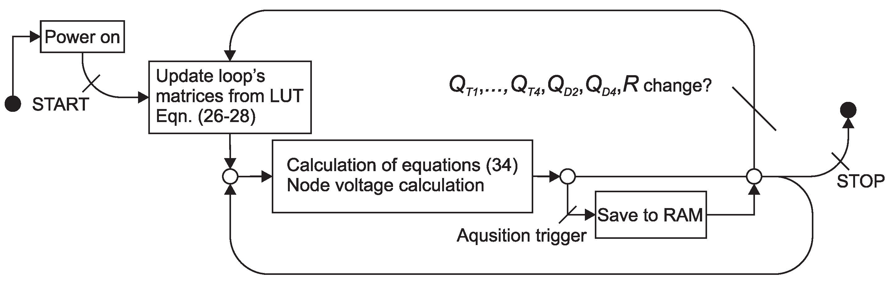
2.4. Off-Line Data Calculation

For faster execution of the FPGA programme, two LUTs (Look Up Tables) were built off-line with a similar method as that presented in [23,24]. Difference to the compared method is in generation process of the possible scenarios, which here are derived from feasible converter power switches combinations, and different data calculation. Firstly, reference voltage signal calculation was performed, and, as result, reference LUT with modulation signal for PWM was designed by Equation (32):
m i t = U ^ U d c sin ( ω 0 t ) = m I sin ( ω 0 t )
and discretized to a 16-bit fix-point vector with 500 points. Thus, for every PWM period ( T s = 40 μ s), there is different modulation signal value, defined as follows:
m i n T s = U ^ U d c sin ( ω 0 n T s ) = m I sin ( ω 0 n T s ) ; n = 1 : 500
where U ^ is the peak value of output sine voltage, U d c is the constant power source (DC) voltage, and ω 0 = 2 π 50 rad/s. Further explanation of PWM follows in the next subsection. Secondly, LUT was designed for loops matrices. As shown in Table 2 and Figure 6, there are six possible states of converter, which means there are six different loops matrices calculated from Equations (26)–(28) by considering Table 1 and Table 3. The inverse of each loops inductance matrices L 1 , L 2 , . . . , L 6 is calculated before conversion to a fix-point. Loops matrices LUT, shown as Matrix1–Matrix6 in Figure 9, were designed after conversion to fix-point. When all data were prepared in fix-point format, two separate Verilog modules were written automatically in Matlab. These modules can be imported in a Quartus Prime FPGA Design Software project, where main FPGA compilation and programming was performed.

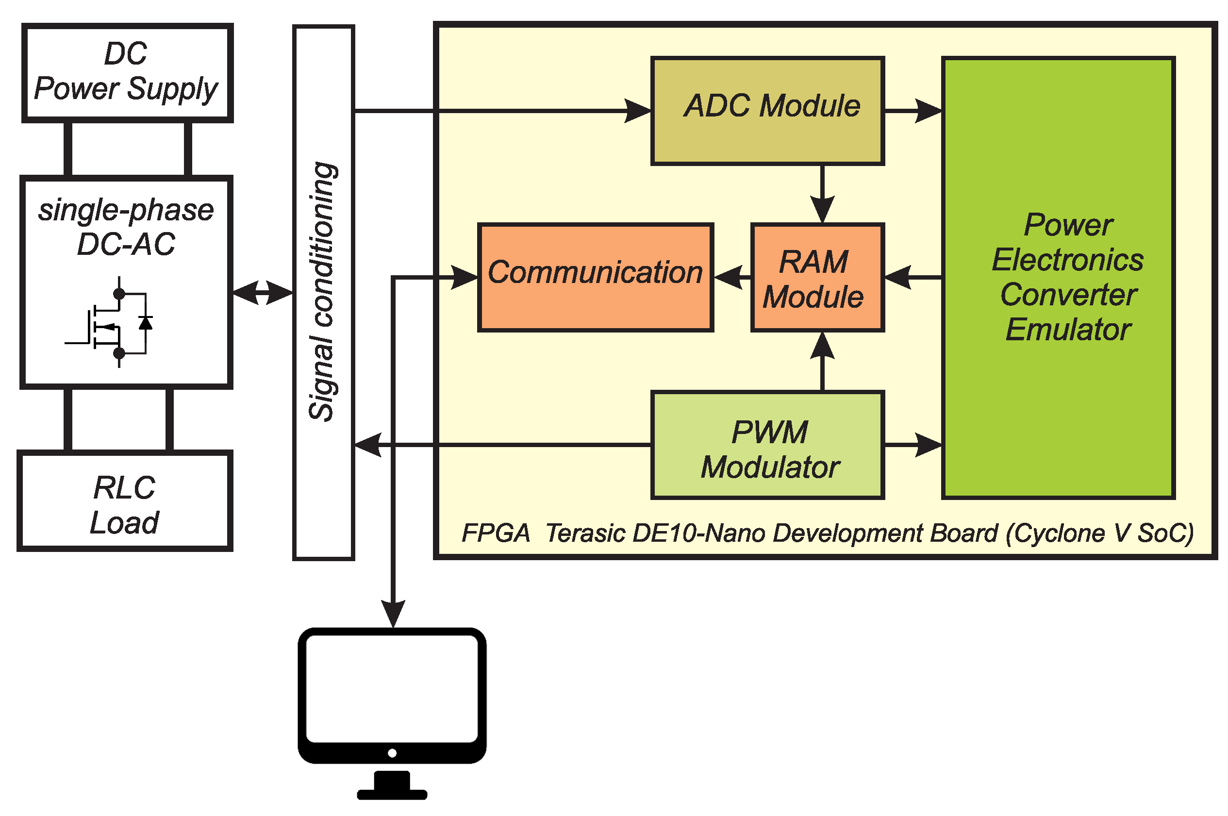
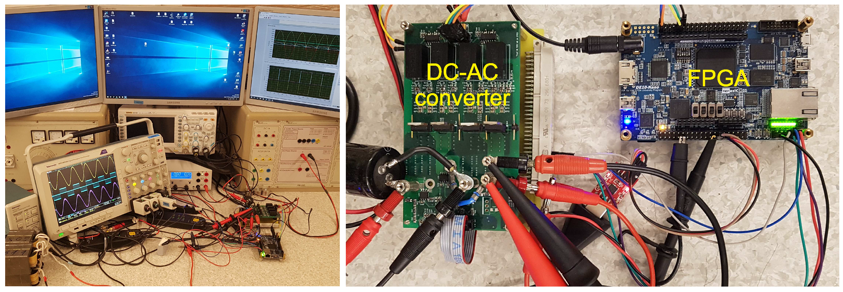
3. Setup for Algorithm Verification

3.1. FPGA Unit

A PWM generator module programmed on FPGA uses an up–down counter with 2000 steps counting at f = 100 MHz, which yields PWM switching frequency f s = 25 kHz. The counter is forming a triangle carrier signal. Gate signal Q T 1 is formed by comparing the modulation signal to the triangle carrier signal as follows:
Q T 1 = 1 ; c o u n t e r m i a n d m i > 0 0 ; c o u n t e r > m i o r m i 0
Gate signal Q T 3 is formed by comparing the modulation signal to the triangle carrier signal as follows:
Q T 3 = 1 ; c o u n t e r m i a n d m i < 0 0 ; c o u n t e r > m i o r m i 0
Gate signals Q T 2 and Q T 4 are negations of their complementary pairs as follows: Q T 2 = Q ¯ T 1 and Q T 4 = Q ¯ T 3 . Each gate signal also has on-delay for 300 ns as a dead time generator. Diodes switching signals Q D 2 and Q D 4 are formed as defined in Equation (29).
An Analog to Digital Converter (ADC) was used to measure DC-link voltage, load current and load voltage. ADC measurements are triggered when the PWM generator counter is at value 0. The measurement of these three signals and serial communication to FPGA were taking 6 μ s, hence maximum sampling rate was 166 ksps. Due to synchronised measurement to centre of PWM pulse, update of measured values was taking place every 40 μ s. Measured values are used for load estimation (for updating load resistance in loops matrices LUT), emulator input (gate signals Q x for correct loops matrices LUT values selection and adapting e vector of emulator to actual DC-link voltage), or further regulation and fault detection purposes that will be implemented.
The system emulation module was designed as a Euler differential equation solver, as follows from Equation (25):
i ( k + 1 ) = i ( k ) + h L ( k ) 1 e ( k ) R ( k ) i ( k ) S ( k ) q ( k ) q ( k + 1 ) = q ( k ) + h i ( k )
where h = 1 × 10 7 s is an integration step. This module state diagram can be seen in Figure 10. Values in loops matrices are being updated from corresponding LUTs at every gate signal or load change. Because a great number of parallel and serial calculations have to be done, clocked pipelining was used for the complete emulation system module. The right side of Equation (34) is calculated every FPGA clock cycle (f = 100 MHz) with the loops matrices values that are provided considering input control signals. Then, loop currents and loop charges are converted to branches currents and branches charges using Equation (16). Results are then used in Equation (19), by which branches voltages are obtained. Nodes voltages are calculated with usage of Equation (31).
A data store module was used for very high speed sampling of calculated data by the System emulation module and sending them to the host PC for verification purposes. Acquisition timing and synchronization was done via the FPGA clock post-scaler, which is scalable from a user interface on the Host PC, and triggers for positioning of data store start. Acquisition length is also settable from user interface within the limits of the RAM size synthesised on the FPGA.

3.2. Single-Phase DC-AC Converter

A single phase H-bridge structure, also known as a full-bridge structure, represents one of the fundamental converter topologies in power electronics. It can support bidirectional power flow between an alternating and a constant power source. In terms of power conversion capabilities, it provides a voltage step down feature for transferring power from a constant power source (DC) to an alternating power source (AC), and a voltage step up feature for transferring power in the opposite direction (rectifier or boost operating mode). A single-phase DC-AC converter operating in step-down mode was used for verification of the emulation system. The MOSFET single-phase DC-AC converter was equipped with drivers and appropriate measurement circuits.

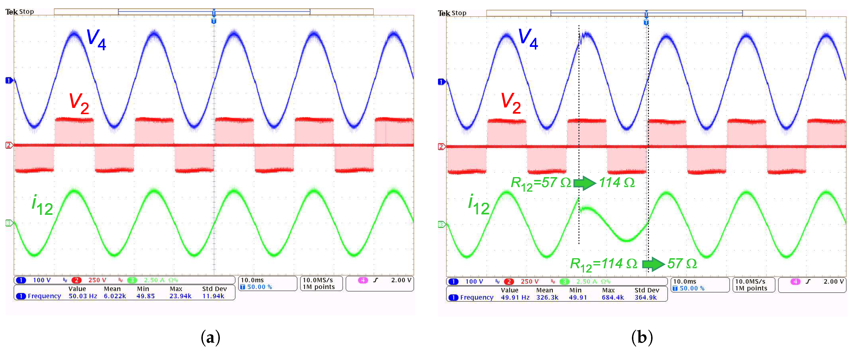
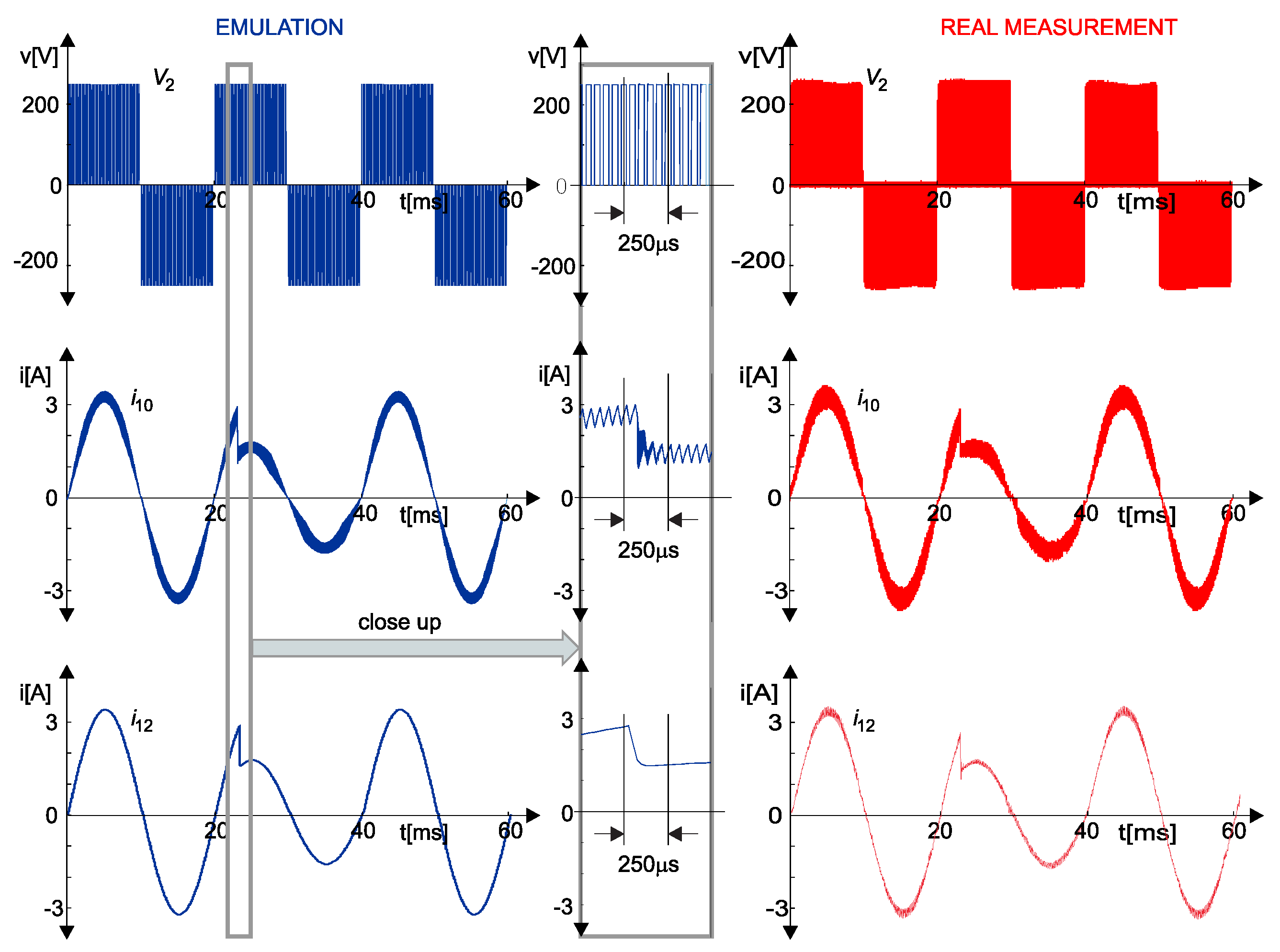
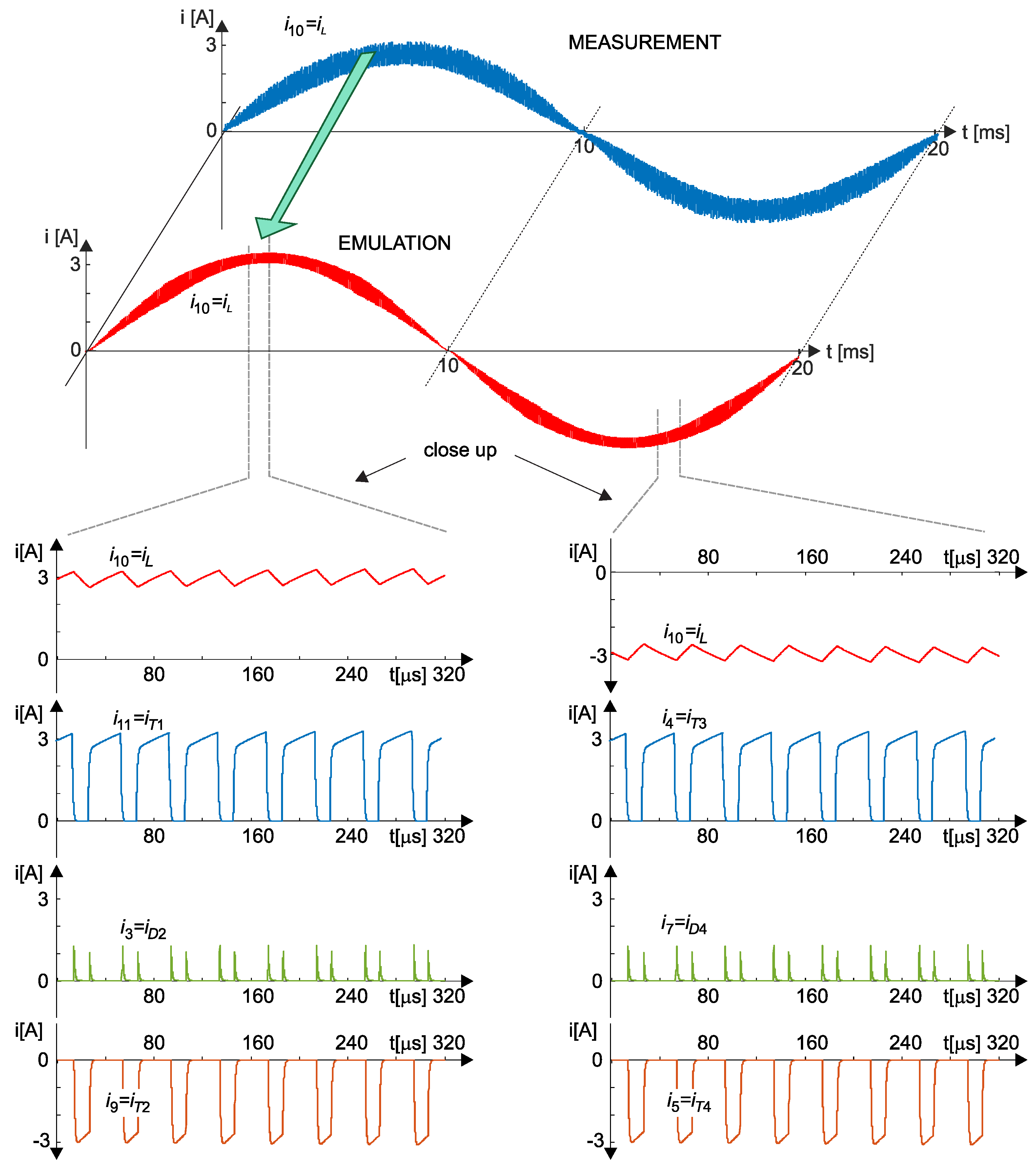
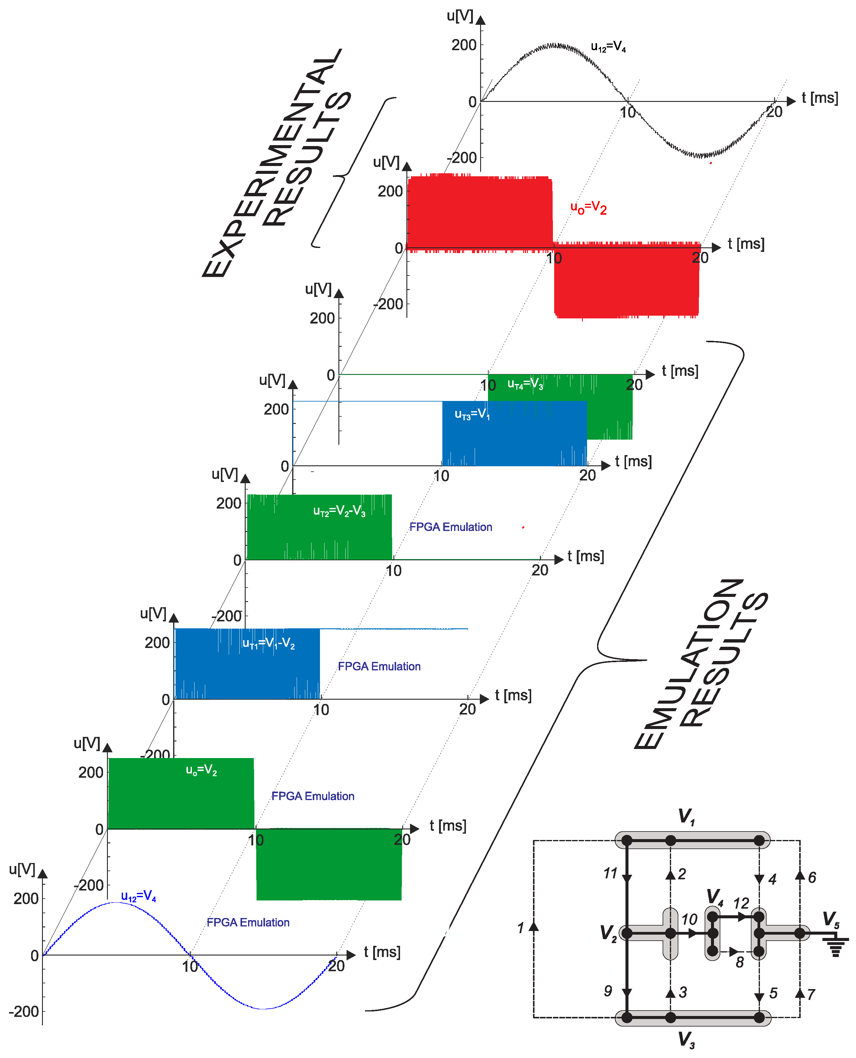
4. Results and Discussion

For verification of the described modelling based on the system in Equation (25), the experimental test-bench system was built, as shown in Figure 8 and Figure 9. Based on the block scheme shown in Figure 1, the real DC-AC converter and Emulation block were built for experimental purposes. The frequency of 25 kHz (end application of household UPS—above audible range) for the PWM triangle carrier was chosen for both the Emulator and real DC-AC converter. Power supply source of U d c = 250 V and the reference voltage (desired output) of u r e f = 0 . 75 · U d c · sin 2 π 50 · t V were chosen. The algorithm was tested under two cases: The first one in the steady state, where load resistance was a constant R = 57 Ω ( R 12 in network topology representation), and the second one, where the load resistance was changed from R = 57 Ω to R = 114 Ω and vice versa. The results of these experiments are shown in Figure 11. To compare the experimental results with the emulated ones, synchronous calculation was performed according to triggering signals. The emulated and real DC-AC converter were exited with the same gate signals Q T 1 Q T 4 . The measured results from the oscilloscope are written to “comma separated values; CSV” file, and, during the emulation, the results were written into the available RAM module. Afterwards, the waveforms were extracted and displayed, as shown in Figure 12, Figure 13 and Figure 14.
Figure 12 shows the emulated and measured voltages on the converter output indicated by V 2 , inductor currents i 10 and resistor currents i 12 . The obtained results are in a good accordance between emulation and experimentation during the load change. The emulation system enables the observation of any converter variable, component voltages and/or component currents. The emulation system is based on Equation (34), so the loops currents have been calculated. By using the developed tie-set matrix, the branch currents were evaluated as linear transformation of loops currents as follows from Equation (15). Figure 13 shows all of the calculated currents in every converter branch. Emulation and experimental results are marked. All current waveforms directions are indicated according to the graph branches orientation. The emulation system also enables the study of variables in close-up, which is shown in Figure 14. The parts of the positive and negative inductor currents (branch i 10 ) are shown as close-up. The currents can also be seen through semiconductors (transistors and diodes). These are almost impossible to measure on the real converters. These variables can be used for evaluation of possible malfunctions of the semiconductors in fault-tolerant circuits. According to the applied PWM procedure, it is also possible to see the diodes in operation. Diodes are active during the dead-time, which is applied to gate signals ( Q T 1 to Q T 4 ) in order to avoid short circuits in both converter legs.
Figure 15 shows all the calculated voltages on every node in the DC-AC converter. The emulation results are in good accordance with the measured ones. To evaluate the voltages, firstly, Equation (19) was calculated, and then, by using these results with Equation (31), the voltages were evaluated on all nodes. The signs of all calculated voltages are in accordance with the voltage drops indicated by arrows in the converter graph.

5. Conclusions

An emulator for a DC-AC converter is described in this paper. Using the graph network theory with the proposed approach enables organising the converter mathematical model with the differential equations system. With the help of the tie-set and reduced incidence matrices, all converter currents and voltages can be calculated. Using PWM signals in the converter loops matrices ( R , S and L ), the branch values, where semiconductors are placed, were changed to introduce the switching behaviour of the MOSFETs and diodes of the DC-AC converters. As follows from the algorithm, the loops inductance inverse matrix L 1 should always be calculated when switching actions occur. Due to the requirement that the emulation process must be performed synchronously with the real converter operation, this task is impossible to solve in real-time. This problem was solved by studying the converter operations, and six inverse matrices were pre-calculated and written in LUT, which were available during the used integration method, and, used correctly, when switching action occurs.
In future work, the focus will be on using the described algorithm for fault tolerant DC-AC converters systems to improve the safety integration level. In addition, the authors would like to extend the used algorithm to other PECs circuits, especially for three-phase systems. The comparison will be done between real and emulated converter total harmonic distortion to check the influence of emulator model parameters and tweak them for better analogy.

Author Contributions

J.M. and M.M. conceived, designed and performed the algorithm necessary for emulation of the PECs, J.M. and M.T. designed the hardware, including the DC-AC converter and test-bench system. M.R. helped in off-line Matlab tasks and communication protocols for the experimental set-up. All authors contributed analysis tools, analysed the data and wrote the paper.

Funding

The authors acknowledge the financial support from the Slovenian Research Agency (Research Core Funding No. P2-0028).

Conflicts of Interest

The authors declare no conflict of interest.

Abbreviations

The following abbreviations are used in this manuscript:
PECPower Electronics Converter
FPGAField-Programmable Gate Array
PWMPulse-Width Modulation
FDFault Diagnosis
HiLHardware in the loop
LUTLook-Up Table
PESPower Electronics System
DSPDigital-Signal-Processor
KCLKirchhoff’s Current Law
KVLKirchhoff’s Voltage Law
ADCAnalog to Digital Converter
U D C Constant Power Source (DC) Voltage
T 1 , T 2 , T 3 , T 4 Converter MOSFET switches
D 1 , D 2 , D 3 , D 4 MOSFETs body diodes
L, R, CConverter output filter and load
b T number of tree branches (or twigs)
nnumber of graph nodes
bnumber of graph branches
A i Incidence matrix
A Reduced incidence matrix
A T Transpose of reduced incidence matrix
NNumber of rows in reduced incidence matrix
a j i Incidence matrix element ( j 1 . . . n , i 1 . . . b )
i b Branch current vector
v i Graph branch voltages
V j Graph nodes voltages
v b Branch voltage vector
V N Node voltage vector
b Number of graph links (or f-loops)
B Tie-set matrix or fundamental loop matrix
B T Transpose of tie-set matrix or fundamental loop matrix
i i Graph branch currents
i j Graph link (or f-loops) currents (j in Roman numbers)
i Link (or f-loops) current vector
e i Branch voltage sources
R i Branch resistances
L i Branch inductances
S i Branch elastances ( S i = 1 C i )
q i Branch charges (i.e., branch capacitor voltages)
e b Branch voltage sources vector
R b Branch resistances diagonal matrix
L b Branch inductances diagonal matrix
S b Branch elastances diagonal matrix
q b Branch charges vector (i.e., capacitor voltages vector)
e Loops voltage sources vector
R Loops resistances matrix
L Loops inductances matrix
S Loops elastances matrix
q Loops charges vector (i.e., capacitor voltages vector)
Q T 1 , Q T 2 , Q T 3 ,Transistor gate signals and diode switching signals, respectively
Q T 4 , Q D 2 ,
and Q D 4
R o n , L o n Conducting model value of resistance and inductance for MOSFETs and diodes
R o f f , L o f f Non-conducting model value of resistance and inductance for MOSFETs and diodes
f s PWM Frequency
T s PWM period
u r e f Modulation reference voltage function
U ^ Peak value of reference output sine voltage
ω 0 Sine reference output signal angular frequency
fFPGA clock frequency
hIntegration step
PCPersonal Computer
RAMRandom-Access Memory
CSVComma-Separated Values

References

  1. Kinsy, M.; Khan, O.; Celanovic, I.; Majstorovic, D.; Celanovic, N.; Devadas, S. Time-Predictable Computer Architecture for Cyber-Physical Systems: Digital Emulation of Power Electronics Systems. In Proceedings of the 2011 IEEE 32nd Real-Time Systems Symposium, Vienna, Austria, 29 November–2 December 2011; pp. 305–316. [Google Scholar] [CrossRef]
  2. Yang, L.; Wang, J.; Ma, Y.; Wang, J.; Zhang, X.; Tolbert, L.M.; Wang, F.F.; Tomsovic, K. Three-Phase Power Converter-Based Real-Time Synchronous Generator Emulation. IEEE Trans. Power Electron. 2017, 32, 1651–1665. [Google Scholar] [CrossRef]
  3. Geng, Z.; Hong, T.; Qi, K.; Ambrosio, J.; Gu, D. Modular Regenerative Emulation System for DC–DC Converters in Hybrid Fuel Cell Vehicle Applications. IEEE Trans. Veh. Technol. 2018, 67, 9233–9240. [Google Scholar] [CrossRef]
  4. De Lillo, L.; Empringham, L.; Wheeler, P.W.; Khwan-On, S.; Gerada, C.; Othman, M.N.; Huang, X. Multiphase Power Converter Drive for Fault-Tolerant Machine Development in Aerospace Applications. IEEE TIE 2010, 57, 575–583. [Google Scholar] [CrossRef]
  5. Zhou, H.; Zhao, W.; Liu, G.; Cheng, R.; Xie, Y. Remedial Field-Oriented Control of Five-Phase Fault-Tolerant Permanent-Magnet Motor by Using Reduced-Order Transformation Matrices. IEEE TIE 2017, 64, 169–178. [Google Scholar] [CrossRef]
  6. Steurer, M.; Edrington, C.S.; Sloderbeck, M.; Ren, W.; Langston, J. A Megawatt-Scale Power Hardware-in-the-Loop Simulation Setup for Motor Drives. IEEE Trans. Ind. Electron. 2010, 57, 1254–1260. [Google Scholar] [CrossRef]
  7. Hazra, S.; Shrivastav, A.S.; Gujarati, A.; Bhattacharya, S. Dynamic emulation of oscillating wave energy converter. In Proceedings of the 2014 IEEE Energy Conversion Congress and Exposition (ECCE), Pittsburgh, PA, USA, 14–18 September 2014; pp. 1860–1865. [Google Scholar] [CrossRef]
  8. Kesler, M.; Ozdemir, E.; Kisacikoglu, M.C.; Tolbert, L.M. Power Converter-Based Three-Phase Non-linear Load Emulator for a Hardware Testbed System. IEEE Trans. Power Electron. 2014, 29, 5806–5812. [Google Scholar] [CrossRef]
  9. Chai, E.; Celanovic, I.; Poon, J. Validation of Frequency- and Time-domain Fidelity of an Ultra-low Latency Hardware-in-the-Loop (HIL) Emulator. In Proceedings of the 2013 IEEE 14th Workshop on Control and Modeling for Power Electronics (COMPEL), Salt Lake City, UT, USA, 23–26 June 2013; pp. 1–5. [Google Scholar] [CrossRef]
  10. Pietrusewicz, K. Metamodelling for Design of Mechatronic and Cyber-Physical Systems. Appl. Sci. 2019, 9, 376. [Google Scholar] [CrossRef]
  11. Dassios, I.; Keane, A.; Cuffe, P. Calculating Nodal Voltages Using the Admittance Matrix Spectrum of an Electrical Network. Mathematics 2019, 7, 106. [Google Scholar] [CrossRef]
  12. Sun, Y.; Tang, X.; Zhang, G.; Miao, F.; Wang, P. Dynamic Power Flow Cascading Failure Analysis of Wind Power Integration with Complex Network Theory. Energies 2018, 11, 63. [Google Scholar] [CrossRef]
  13. Arboleya, P.; González-Morán, C.; Coto, M. Unbalanced Power Flow in Distribution Systems With Embedded Transformers Using the Complex Theory in αβ0 Stationary Reference Frame. IEEE Trans. Power Syst. 2014, 29, 1012–1022. [Google Scholar] [CrossRef]
  14. Zhang, L.; Abur, A. Single and Double Edge Cutset Identification in Large Scale Power Networks. IEEE Trans. Power Syst. 2012, 27, 510–516. [Google Scholar] [CrossRef]
  15. Wang, C.; Zhang, T.; Luo, F.; Li, P.; Yao, L. Fault Incidence Matrix Based Reliability Evaluation Method for Complex Distribution System. IEEE Trans. Power Syst. 2018, 33, 6736–6745. [Google Scholar] [CrossRef]
  16. Saleh, M.; Esa, Y.; Mohamed, A. Applications of Complex Network Analysis in Electric Power Systems. Energies 2018, 11, 1381. [Google Scholar] [CrossRef]
  17. Ma, F.; O’Hare, G.M.P.; Zhang, T.; O’Grady, M.J. Model Property Based Material Balance and Energy Conservation Analysis for Process Industry Energy Transfer Systems. Energies 2015, 8, 12283–12303. [Google Scholar] [CrossRef] [Green Version]
  18. Mostacciuolo, E.; Vasca, F.; Baccari, S. Differential Algebraic Equations and Averaged Models for Switched Capacitor Converters with State Jumps. IEEE Trans. Power Electron. 2018, 33, 3472–3483. [Google Scholar] [CrossRef]
  19. Dörfler, F.; Simpson-Porco, J.W.; Bullo, F. Electrical Networks and Algebraic Graph Theory: Models, Properties, and Applications. Proc. IEEE 2018, 106, 977–1005. [Google Scholar] [CrossRef]
  20. Chen, R.R.; Davis, M. Network Laws and Theorems. In The Circuit and Filters Handbook; Chen, W.-K., Ed.; CRC Press LLC: Boca Raton, FL, USA; London, UK; New York, NY, USA; ashington, DC, USA, 2003; pp. 529–583. [Google Scholar]
  21. Milanovic, M. PWM spectrum evaluation and over-modulation phenomena in a three-phase inverters-analytical approach. In Proceedings of the 2008 13th International Power Electronics and Motion Control Conference, Poznan, Poland, 1–3 September 2008; pp. 301–306. [Google Scholar]
  22. Eisenack, H.; Hofmeister, H. Digitale Nachbildung von elektrischen Netzwerken mit Dioden und Thyristoren. Archiv far Elektrotechnik 1972, 55, 32–43. [Google Scholar] [CrossRef]
  23. Mohagheghi, E.; Gabash, A.; Li, P. A Framework for Real-Time Optimal Power Flow under Wind Energy Penetration. Energies 2017, 10, 535. [Google Scholar] [CrossRef]
  24. Mohagheghi, E.; Gabash, A.; Alramlaw, M.; Li, P. Real-time optimal power flow with reactive power dispatch of wind stations using a reconciliation algorithm. Renew. Energy 2018, 126, 509–523. [Google Scholar] [CrossRef]
Figure 1. The emulator and real DC-AC system architecture appropriate for testing and verification.
Energies 12 00969 g001
Figure 2. (a) Electrical circuit DC-AC converter; and (b) circuit graph.
Energies 12 00969 g002
Figure 3. (a) Oriented graph; (b) Tie-set matrix graph; and (c) Circuit elements.
Energies 12 00969 g003
Figure 4. General branch model.
Energies 12 00969 g004
Figure 5. Gate signals: Q T 1 Q T 4 .
Energies 12 00969 g005
Figure 6. (a) Switch sequences when first leg transistors of DC-AC are switching from T 1 to T 2 ; and (b) switch sequences when second leg transistors of DC-AC are switching from T 3 to T 4 .
Energies 12 00969 g006
Figure 7. Gate signals when: (a) positive half-period output voltage is required; and (b) negative half-period output voltage is required.
Energies 12 00969 g007
Figure 8. Experimental test-bench system.
Energies 12 00969 g008
Figure 9. Block scheme, signal-flows, branch elements.
Energies 12 00969 g009
Figure 10. System emulator state diagram.
Energies 12 00969 g010
Figure 11. Load measurements (x-axis 10 ms/div): (a) constant load resistance, voltages; blue curve V 4 , y-axis 100 V/div; red curve V 2 , y-axis 250 V/div; current, green curve i 12 , y-axis 2.5 A/div; and (b) step change into load resistance, voltages; blue curve V 4 , y-axis 100 V/div; red curve V 2 , y-axis 250 V/div; current, green curve i 12 , y-axis 2.5 A/div.
Energies 12 00969 g011
Figure 12. Emulation results and its close-up (blue curves) and measured results (red curves).
Energies 12 00969 g012
Figure 13. Results of emulation and measurement currents.
Energies 12 00969 g013
Figure 14. Emulation and measurement results of inductor current and close up of emulated: inductor current ( i 10 ), MOSFETs currents ( i 4 , i 5 , i 9 and i 11 ) and diodes currents ( i 3 and i 7 ).
Energies 12 00969 g014
Figure 15. Results of emulation and measurement voltages.
Energies 12 00969 g015
Table 1. Matrix elements for transistors controlled by PWM.
Gate Signals T 1 T 2 T 3 T 4
Q T i = 1 R 11 = R o n R 9 = R o n R 4 = R o n R 5 = R o n
i = 1 , 2 , 3 , 4 L 11 = L o n L 9 = L o n L 4 = L o n L 5 = L o n
Q T i = 0 R 11 = R o f f R 9 = R o f f R 4 = R o f f R 5 = R o f f
i = 1 , 2 , 3 , 4 L 11 = L o f f L 9 = L o f f L 4 = L o f f L 5 = L o f f
Table 2. PWM generator error detection.
# Q T 1 Q T 2 Q T 3 Q T 4 Q D 2 Q D 4 Error
00000xx0
100011x0
20010xx1
30011xx1
40100x10
50101000
60110x00
70111xx1
81000xx1
910010x0
101010xx1
111011xx1
121100xx1
131101xx1
141110xx1
151111xx1
Table 3. Matrix elements for diodes controlled by gate signals Q D 2 and Q D 4 .
Gate Signals D 2 D 4
Q D i = 1 R 3 = R o n R 7 = R o n
i = 2 , 4 L 3 = L o n L 7 = L o n
Q D i = 0 R 3 = R o f f R 7 = R o f f
i = 2 , 4 L 3 = L o f f L 7 = L o f f

