1. Introduction
A Single Input Multi Output (SIMO) and Multi Input Multi Output (MIMO) DC-DC converters have the ability to provide different voltage and current levels and eliminate the drawbacks of having bulky inductors for each output. MIMO converters can have two or more diversified renewable energy sources with variable dc voltage and current characteristics. The outputs of the converters can be configured either independently where all the output ports share the same ground or the outputs can be connected in series fashion. Both the converters can be operated either in Continuous Conduction Mode (CCM) or in Discontinuous Conduction Mode (DCM) and mode selection depends on the load current rating and the amount of ripples in the output voltages. In this paper, CCM mode capable of handling the large current load with lesser ripples is taken. Like all converters, compensators and/or controllers are essential to improve the time and frequency domain specifications with the additional constraint of reducing cross regulation. To achieve these goals different control techniques are available in the literature for both the converter types.
For SIMO converters, to achieve good regulation performance over wide load current and voltage ranges with fewer ripples and high efficiency, different control algorithms are developed based on the output voltages or inductor current. In reference [
1], cross-regulation is minimized by operating in hysteresis mode with additional circuitry, but there is a reduction in efficiency due to the flow of current in the freewheeling switch. In reference [
2], time multiplexing techniques to regulate the multiple output voltages and to reduce cross-regulation are proposed but the output voltages have higher amount of ripples. To reduce ripples and cross regulation, the zero current switching lagging leg is added which makes the circuit more complex [
3]. In reference [
4], the Single Inductor Dual Output (SIDO) boost converter with discrete pulse width modulation is proposed which occupies lesser area and operates at higher efficiency only when the system works for low power applications. In reference [
5], to increase the voltage gain, two half bridge converters are formed in series manner with clamp circuit such that the soft switching is obtained with reduced stress on switches. Modelling of SIMO dc-dc converters in particular for two outputs is done in [
6] and most of the researchers have used this model only to design the controllers for SIDO Buck converter [
7]. Also, in reference [
7], multivariable digital control for SIDO converter is designed using the model in [
6] where a system open loop transfer function matrix is shaped by convex minimization method to decouple the system. In another research, an inductor current ripple-based modelling approach is proposed to model and analyze the converter accurately. The control, cross coupling, and cross regulation transfer functions, generated with the model has been portrayed in [
8]. However, the procedure involved is very complex and lengthy. A ripple-based modelling of the SIDO buck converter is developed for cross derivative state feedback control methodology in [
9]. The number of compensators required is two times that of the outputs and the parameters of the compensators are obtained using trial and error method. The algorithm used to develop a model is complex and limited to two outputs. The analysis is done only for SIDO system and there is no generalized mathematical model of SIMO and MIMO converters for ‘
n’ number of outputs. This emphasis necessitates the development of a generalized mathematical model for SIMO dc-dc converter with n number of independent outputs considering the on-state losses of the switches. It helps to analyze the steady state and dynamic performance of the converter.
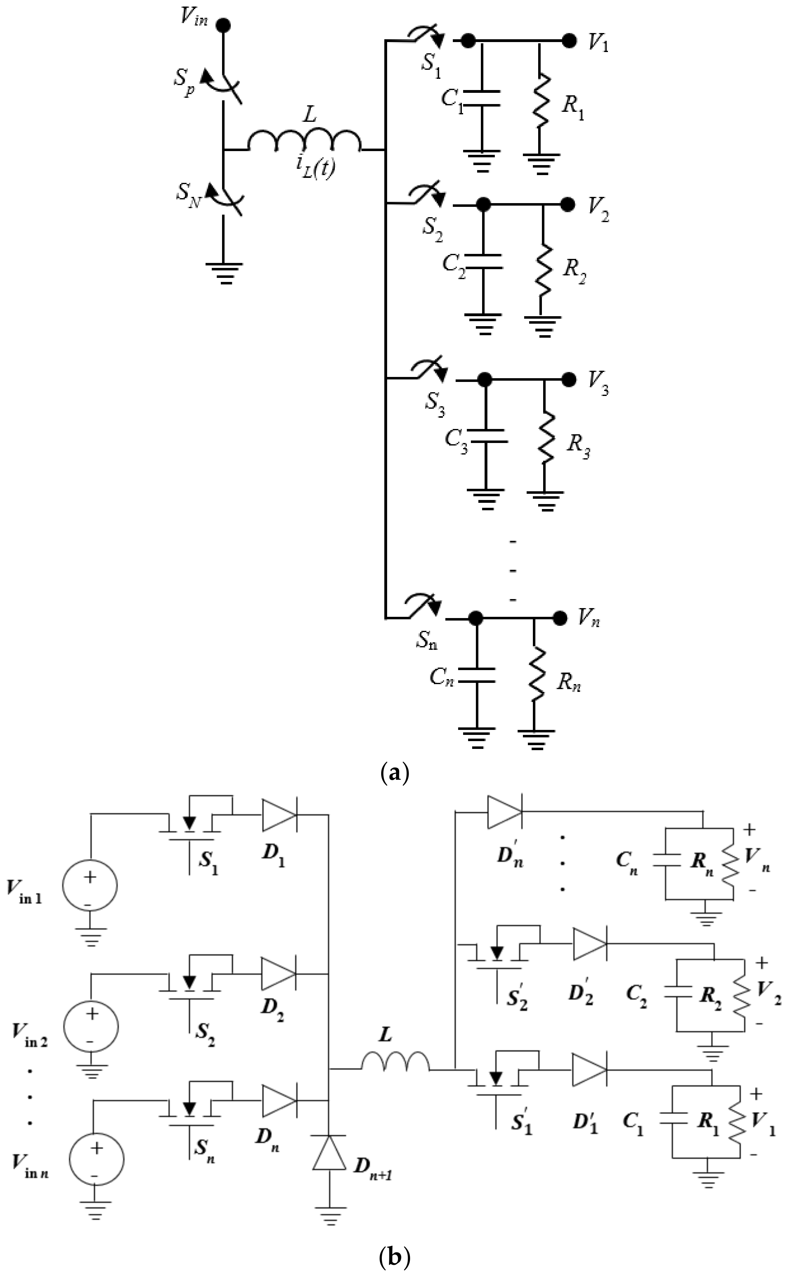
Electric vehicles, energy harvesting applications, and DC micro-grids are typical examples of MIMO system where the inputs can be from various sources and the loads will have different voltage/current specifications. MIMO converters are cost effective solutions and can be operated in DCM or CCM modes. In DCM, the limitation is with the maximum inductor current and thereby high-power applications are not possible. In reference [
10], the topology is introduced to interface the multiple output dc-dc converters with diode clamped inverter but the detailed analysis on control strategies is not present. The analysis on the design of a multivariable controller for MIMO system is introduced in [
11]. But the outputs are connected in a series manner and there is no generalized mathematical model for ‘
n’ number of outputs. A linearized small signal ac model is developed for two outputs in which the outputs are connected in series configuration [
11]. The above model has to include
n + 2 number of variables for the design of controllers. Therefore, a new topology is developed in which the outputs are connected independently and share lesser number of switches.
To eliminate the complexity in designing controller for higher number of outputs, linear, non-linear and intelligent controllers separately in multi loop mode are proposed [
12]. Naturally, multivariable controllers are suited for the SIMO and MIMO converters [
13]. Multivariable control, which reduces the number of controllers used in the system, appears to be a promising technology for the targeted space restricted applications.
The suitability of multivariable control for the SIMO and MIMO systems with Evolutionary Algorithms can be found in [
14] which uses a Artificial Bee Colony algorithm with variable population size. Its focus is mainly on the convergence of the algorithm for a Multivariable PID controller applied in a Distillation Column Systems, a 2 × 2 multivariate process with strong interactions between the inputs and outputs. Particle Swarm Optimization-based multivariable PID controller performance [
15] is found to be better than the Ziegler Nicholas method for a MIMO process. A Twin Rotor System where LQR whose weighted matrix elements are found by a Bacterial Foraging Algorithm is shown to be better than a manually calculated/found weighting matrix [
16]. In reference [
17], a randomized algorithm is presented for the design of an optimal PID controller for MIMO systems such that the closed loop poles are placed at desired locations to obtain the desired performance specifications. Therefore, simplicity and availability of global optimization techniques to search for best parameters and design procedure using the model of the system are the compelling reasons for studying multivariable PID and optimal LQR for the SIMO and MIMO systems. Ninety percent of the controllers used are PID controllers which is most discussed, analyzed and tested with flexibility and robustness for most of the applications. Optimal LQR controller for MIMO systems are extensively studied in the literature and the superiority of the controller over other controllers are well documented [
18].
In this paper, the simplified small signal mathematical models of SIMO and MIMO converters including on-state resistance of the switches are developed for n number of outputs. From these models, small signal models of the converter for any number of outputs can be obtained. These models also used to obtain the control inputs to output voltages and input voltages to output voltages transfer functions of both SIMO and MIMO dc-dc converters for any number of outputs. Here multivariable PID and optimal LQR controllers are developed for SIDO and DIDO converters. The parameters of these controllers are obtained with the help of GA based optimization tool using developed small signal models of the converter and reduction in the coupling between the outputs are done. Gershgorin bands drawn for the converters before and after adding the controller serve as a tool to show the amount of coupling between the outputs. The designed controllers are validated by using DT 9834® Data Acquisition Module. From both the simulated and hardware results, it is revealed that LQR performs well for both the systems.
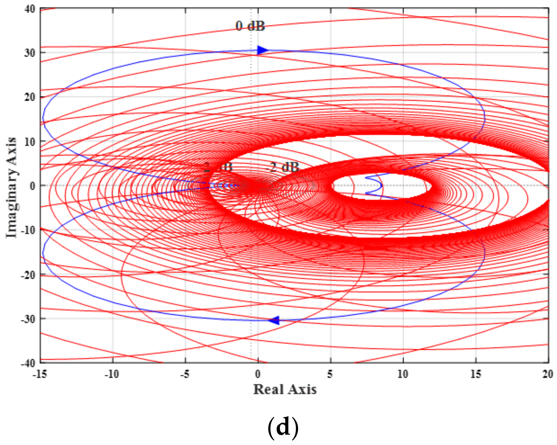
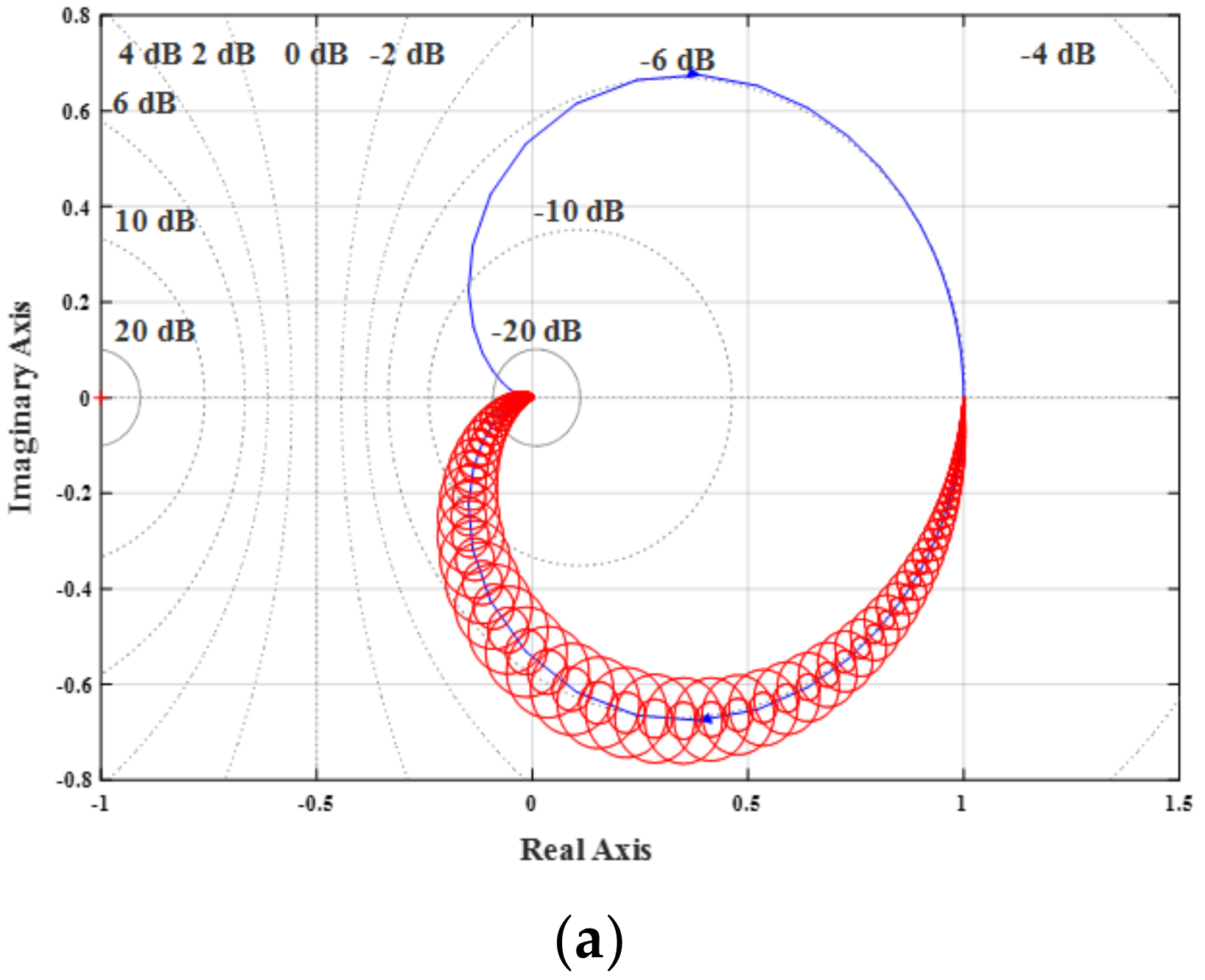
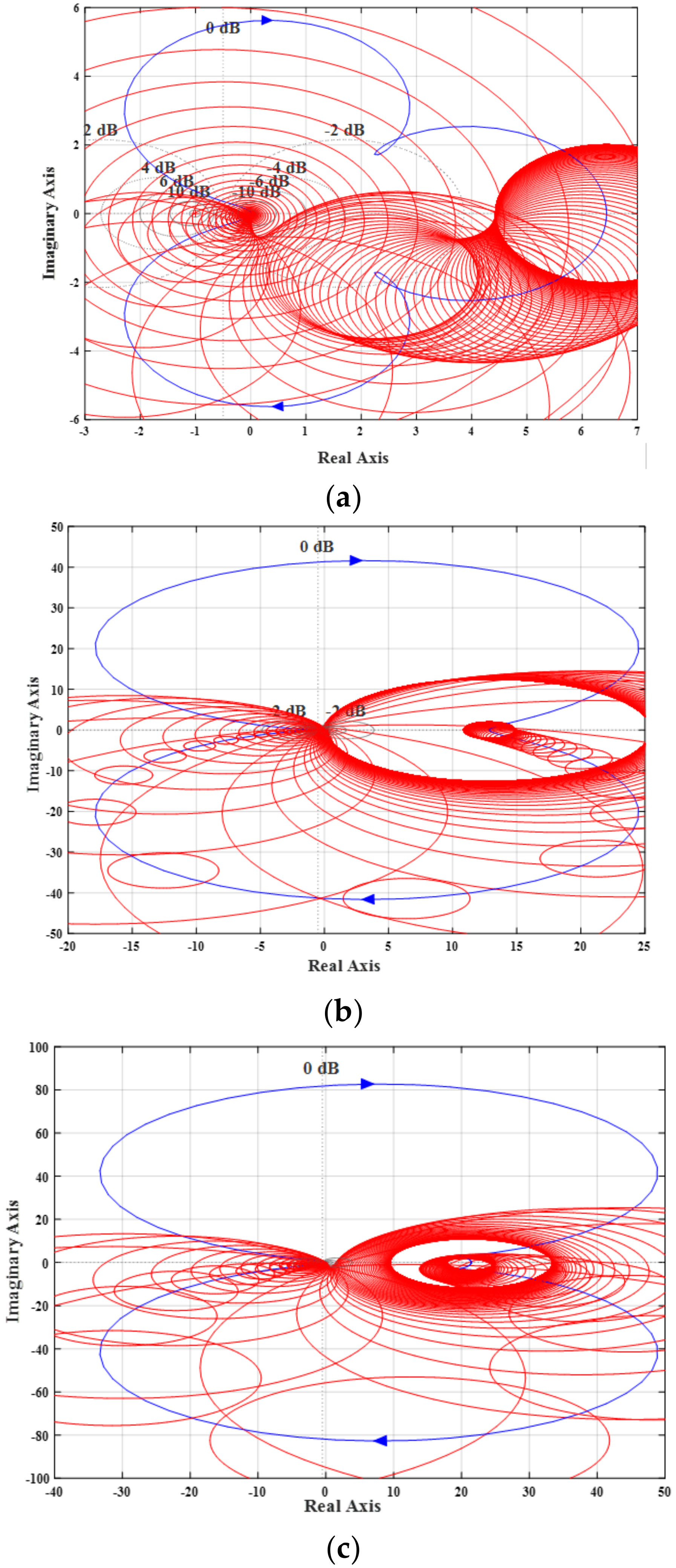
3. Study on Coupling and Stability
Gershgorin and Relative Gain Array (RGA) are two techniques to identify the coupling between the outputs and control inputs. Gershgorin circle is drawn at each point of the Nyquist plot of the diagonal elements
gii(
s) with the following radius
or
where
n is number of inputs and outputs to check for coupling where the coupling denotes the presence of the cross regulation. The set of circles drawn with above radius enclosing the locus of
gii(
ω) is called as Gershgorin bands. Gershgorin theorem reveals that the bands catch the unions of the Nyquist diagram and moreover helps to say that there will be as many Nyquist diagrams trapped in a region as many Gershgorin bands are there. The stability of the system is identified by counting the number of endings made by the bands around the point (−1, 0). If the bands are thin and exclude the origin then it is found that the system is diagonally dominant which is diagonalized as a de-coupled system [
22]. Such Gershgorin bands are drawn for
g11(
s) and
g22(
s) of SIDO and DIDO converters and shown in
Figure 4.
It is found that the bands are enclosing the origin as the system is not diagonal dominance, that is, it’s a coupled system and hence a controller is required to make the system as decoupled. Moreover, RGA, denoted as ⋏ is used as a parameter to measure the inputs and outputs interactions. RGA for both the systems are given in Equations (20) and (21):
From Equations (20) and (21), it is found that both the matrices are not diagonal which indicates that the output one gets varied due to change in both the control inputs.
5. Genetic Algorithms for Finding Parameters of Multivariable PID and LQR Controllers
Genetic Algorithm (GA) is an optimization tool which mimics natural evolution in finding the best solution. It is useful when the search space is large and unknown with local minima’s [
23]. It starts with a set of solutions (population) represented as bit strings or rational numbers and by processes such as crossover, mutation and selection evolves to a better solution. In this paper, the population is rational numbers and the tuning of GA process is done for fast convergence as per the steps followed in [
24]. SIMO and MIMO are non-linear systems where tuning of controller parameters becomes extremely difficult when the number of inputs and/or outputs increases. They have mutual interferences which have to be nullified and tuning of controller parameters has to decouple the same. In these systems, GA is used to find cyclic matrix of multivariable PID and weighting matrix of optimal LQR controllers. These matrices are multimodal in nature with many dimensions [
24] and this is where conventional optimization techniques fail whereas global optimization algorithms such as GA accommodate these constraints [
25,
26]. In addition, GA are computationally simple and have inherent parallelism. Successful applications are further seen related to multivariable PID and optimal LQR for MIMO process in [
27,
28,
29].
The objective function can be either Integral Square Error (ISE), Integral Absolute Error (IAE), Integrated Time Absolute Error (ITAE) or a combination of all and has to be minimized. The objective function is the sum of various parameters related to time response such as Rise Time, Settling Time, Overshoot, Peak Time and Undershoot [
30]. The parameters used to study the performance analysis of the controllers are Overshoot, Undershoot, Settling Time, Ripples and Cross Regulation. Overshoot, Undershoot and Ripples relate to the quality of the response whereas Settling Time measures the speed of the response. In SIMO and MIMO converters the main parameter to consider is the Cross Regulation which is change of desired level in an output due to disturbance in other outputs or inputs. Each parameter has to be given a weight (
Wn) since some parameters values are relatively very high and dominate the convergence and weights are found out by trial and error method. Another method is running the GA with few dominant parameters and then stopping the GA and continuing it again with all parameters from the population until it is stopped:
Equation (22) gives the objective function taken for this problem in which the overshoot_2 (which is cross regulation) is taken as the dominant factor.
7. Design Algorithm
Let
λ1,
λ2 …
λn+p be the desired poles. The desired characteristic polynomial is:
where
and
Equating the Equations (30) and (31), the parameters of the PID controller can be obtained. The (
n +
p)th order state model of the closed loop system is then given by:
The design procedure is summarized as follows:
- (1)
The system description (, , ) and the desired pole positions λ1, λ2 … λn + p are obtained from the mathematical model.
- (2)
Genetic Algorithm-based optimization is used to obtain the value of Ξ matrix.
- (3)
Develop a coding procedure to find the control signal Λ.
- (4)
Check the response of the system for a unit step input.
- (5)
If desired objectives are not obtained, tuning of GA is performed again to obtain the new value of Ξ either by changing the values of closed loop poles or by k matrix.
The
matrix found for SIDO is given by the Equation (34):
The corresponding
Kp,
Ki and
Kd values obtained are given in Equations (34)–(36), respectively:
The Multivariable PID controller is able to make the closed loop poles to lie at the following locations: P1 = (−1500 + 1000i), P2 = (−1500 − 1000i), P3 = (−1000 + 200i), P4 = (−1000 − 200i) and P5 = (−500).
Similarly, the
matrix found for DIDO is given by the Equation (38):
The corresponding
Kp,
Ki and
Kd values derived from the
Q matrix are given in Equations (39)–(41):
Similarly, the closed loop poles obtained after adding multivariable PID controller are given below: P1 = (−500 + 2171.5i), P2 = (−500 − 2171.5i), P3 = (−335.9 + 571.1i), P4 = (−335.9 − 571.1i) and P5 = (−806.3).
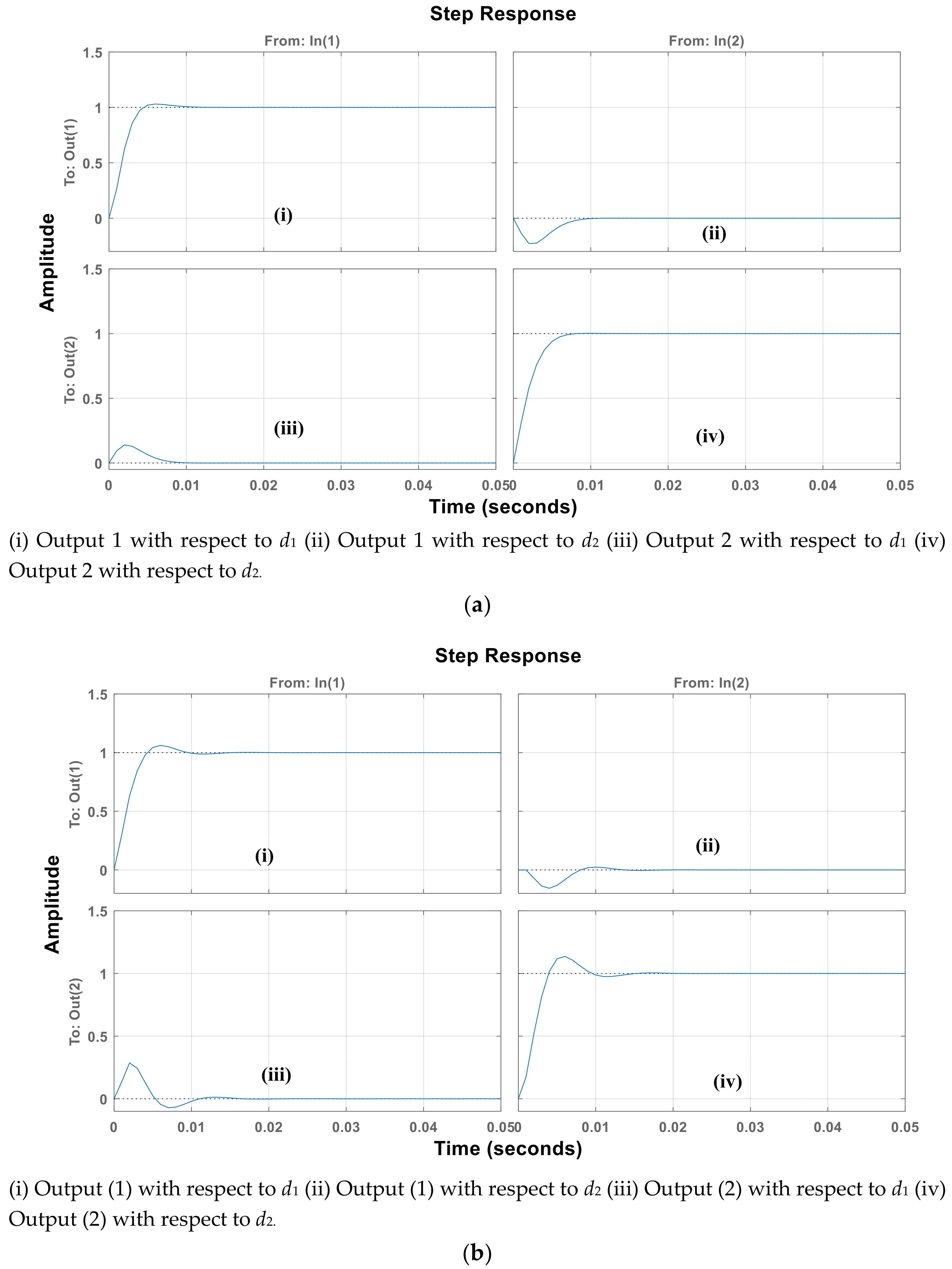
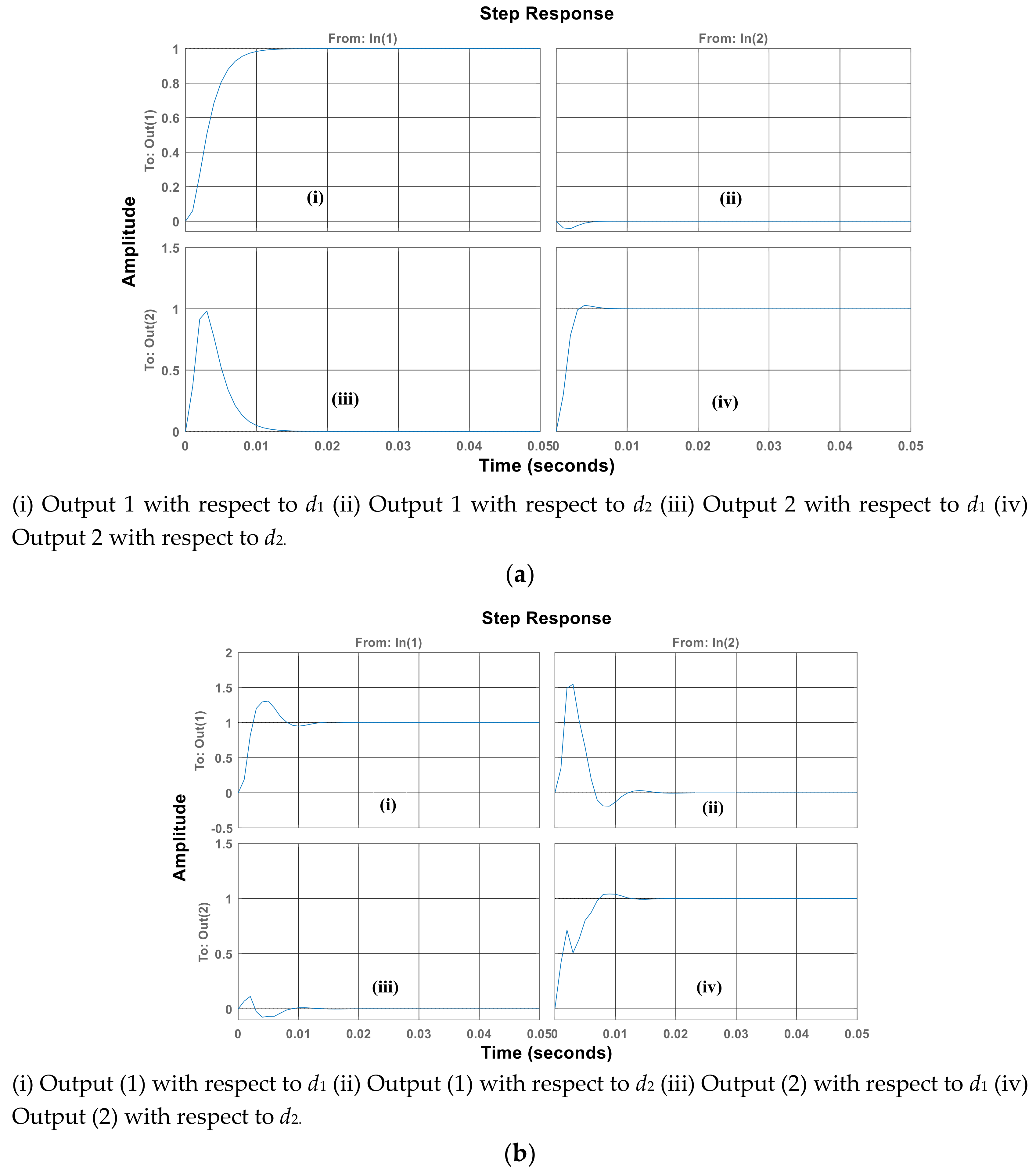
The response of the unit step function for the controllers taken into study using MATLAB
® m-file coding is shown in
Figure 7a,b for SIDO and DIDO, respectively.
Figure 7a,b reveal that the system has become decoupled one due to the addition of multivariable PID controller.
Figure 7a (i) and (iv) and
Figure 7b (i) and (iv) show that both the output voltages
V1 and
V2 obey only for their respective control inputs
d1 and
d2 respectively.
Figure 7a (ii) and (iii) and
Figure 7b (ii) and (iii) reveal that the output voltages
V1 and
V2 do not respond to the control inputs
d2 and
d1 respectively and produce zero outputs as the system has become decoupled one. The converters and the multivariable PID controller are developed using discrete components available in MATLAB SIMULINK
®. The results are shown in
Figure 8 for SIDO converter and in
Figure 9 for DIDO converter.
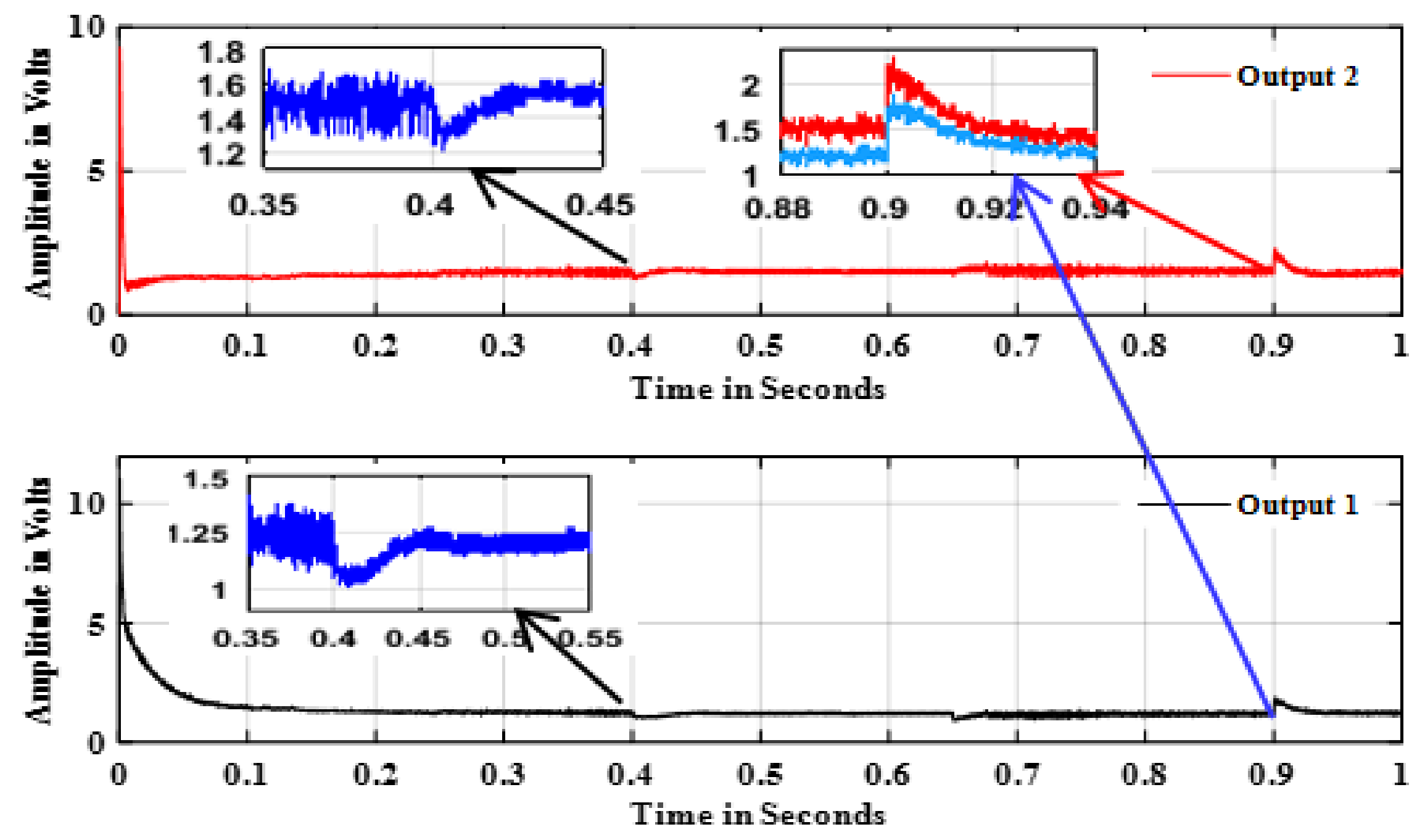
Load disturbance is given at
t = 0.4 s in output 2 by increasing the current from 0.5 A to 1.05 A and the output 2 takes 0.03 s to come back to the value of 1.5 volts. The output 1 has undershoot and takes 0.05 s to come back to the same value. Load disturbance is given at
t = 0.65 s in output 1 by increasing the current from 0.3 A to 0.65 A and the output 2 has overshoot and comes back to the same value with the time period of 0.03 s. The output 1 has undershoot and comes back to the same value in 0.03 s. The supply voltage is increased to 15 V from 12 V and both the outputs have overshoot of increase in 1 V and they settle within 0.03 s. Thus, from
Figure 8, it is evident that the cross regulation is minimized. Good dynamic response (except peak overshoot) is obtained from the multivariable PID controller.
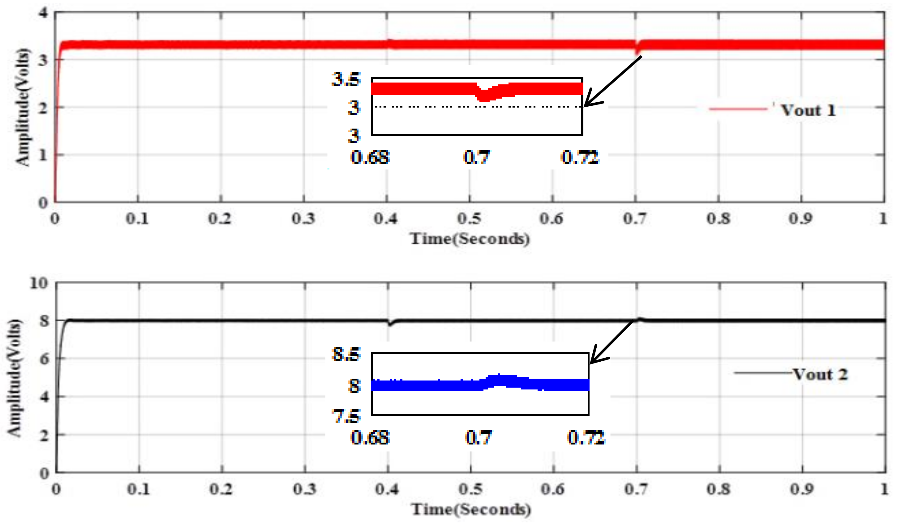
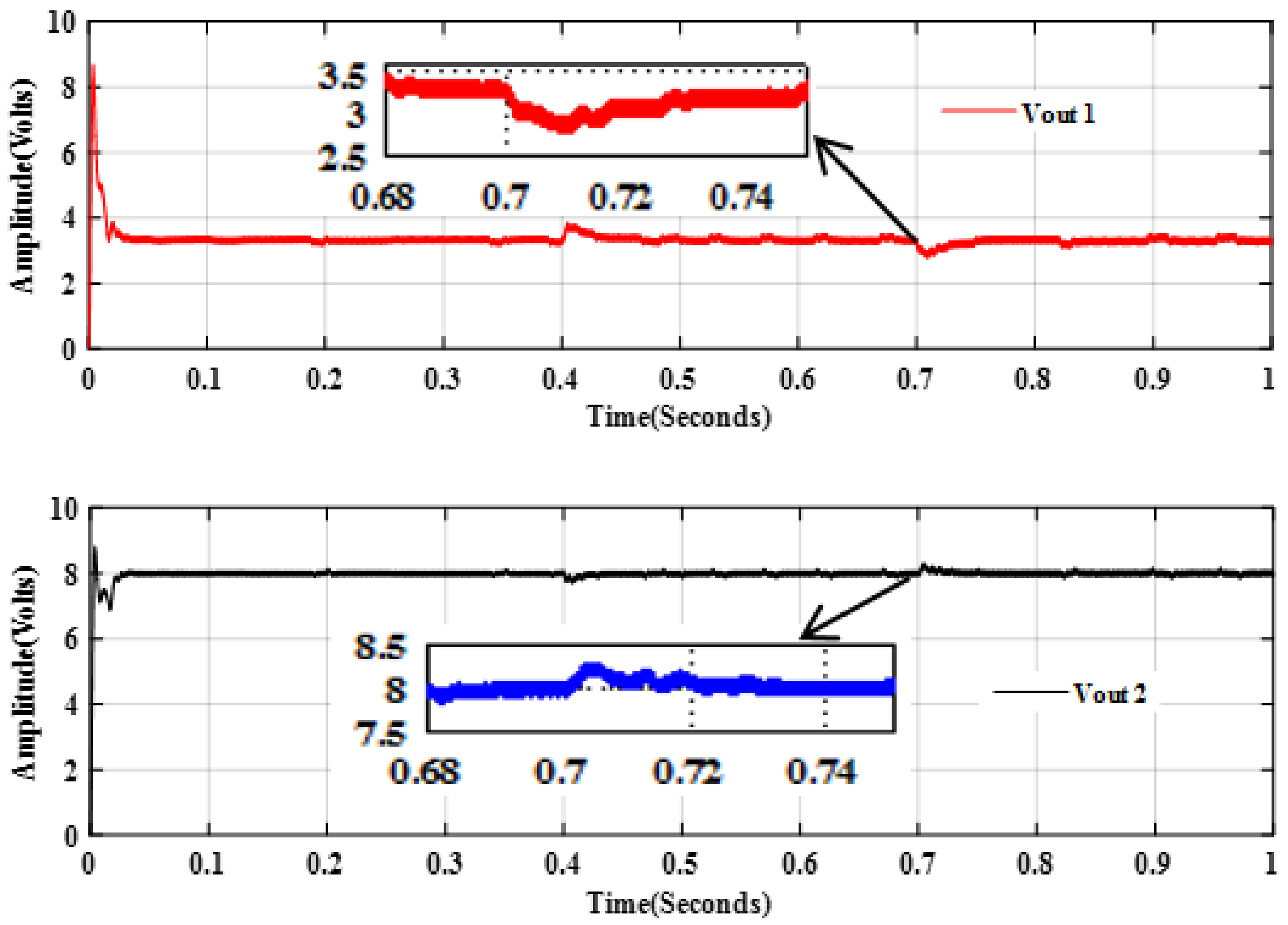
Similarly, for DIDO converters, load disturbance is given at t = 0.4 s in output 2 by increasing the current from 2 A to 2.5 A and the output 1 takes 0.017 s to come back to the value of 3.3 Volts. The output 2 has undershoot and takes 0.032 s to come back to the value of 8 V. Load disturbance is given at t = 0.7 s in output 1 by increasing the current from 2 A to 2.5 A and the output 2 takes 0.02 s to return to the value of 8 V. The output 1 has undershoot and takes 0.03 s to return to the same value.
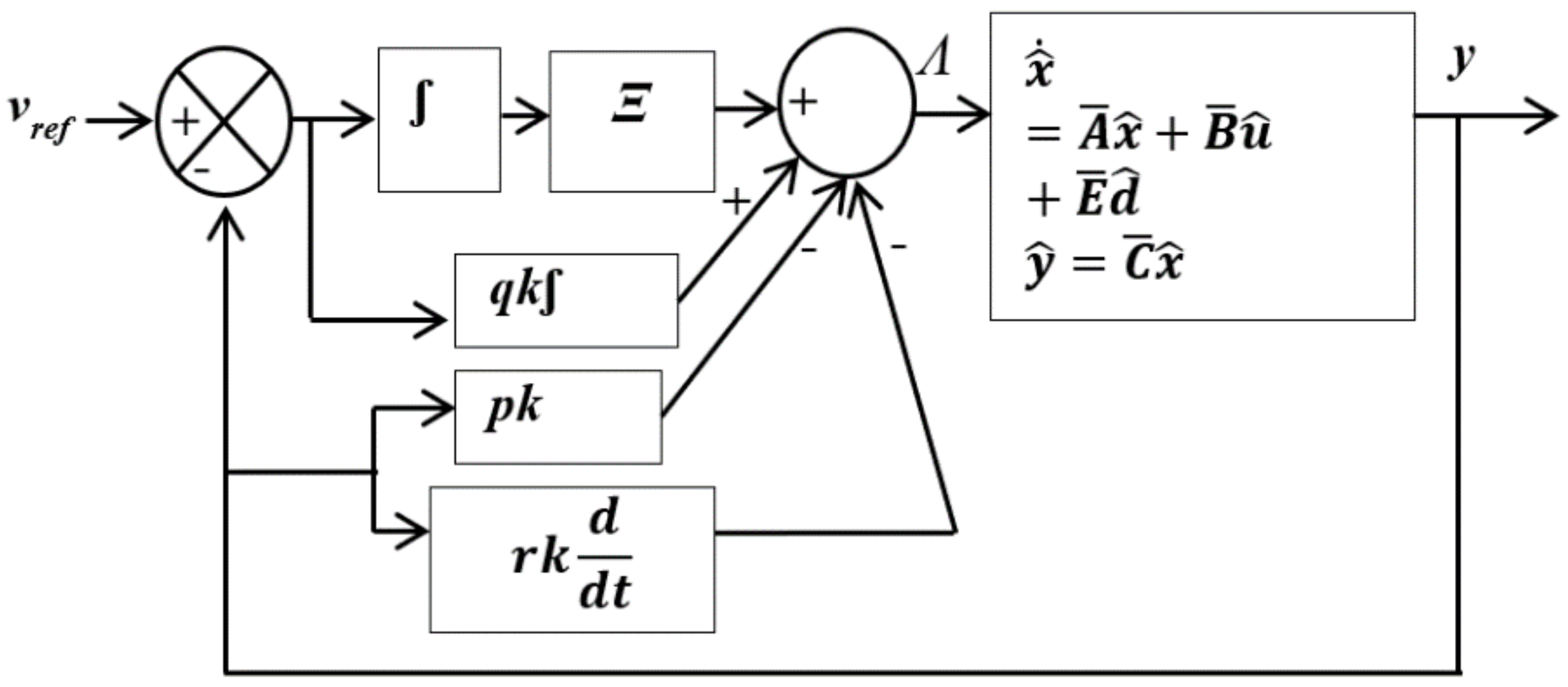
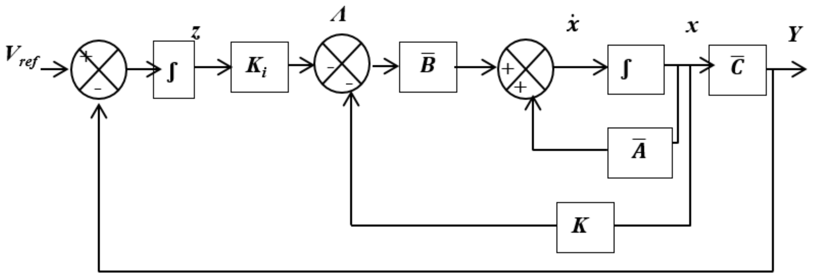
Optimal LQR Controller
Figure 10 shows the block diagram representation of the closed loop system with LQR controller, where the control signal is:
where
k is the feedback gain matrix of order
d ×
p and
ki is the integral matrix of order
n ×
d. The state space model of the closed loop system is given as:
The design procedure can be summarized as follows:
The augmented system matrices are entered and their controllability and observability are checked.
The values of Q and R are obtained using GA based optimization technique.
The value of Ki is assigned based on the knowledge from PID Controller
Algorithm is developed to find the values of the state feedback gain matrix, which is in the order of p × n and check the response for a unit step input.
If desired objectives are not met, tuning of GA is performed.
The
K matrix found for SIDO and is given by the Equation (46):
The corresponding
Ki value used to derive
K matrix and given as Equation (47):
Similarly, the
K matrix found is for DIDO and given by the Equation (48):
The corresponding
Ki value used
Q matrix and given as Equation (49):
The response of the unit step function for the controllers taken into study using MATLAB
® m-file coding is shown in
Figure 11a,b for SIDO and DIDO, respectively.
Figure 11a,b reveal that both the output voltages obey only for their respective control inputs due to the addition of Optimal LQR controller and the outputs are zero due to other inputs. The converters and the optimal LQR controller are developed using discrete components available in MATLAB SIMULINK
®. The results are shown in
Figure 12 for the SIDO converter and in
Figure 13 for the DIDO converter.
The SIDO system performance for load disturbances is given in
Figure 12. Load disturbance is given at
t = 0.4 s in output 2 by increasing the current from 0.5 A to 1.05 A and the output 2 takes 0.01 s to revert to the value of 1.5 V. Output 1 has the undershoot and takes 0.01 s to revert to the same value of 1.2 V. Load disturbance is given at
t = 0.65 s in output 1 by increasing the current from 0.3 A to 0.6 A and the output 2 has overshoot and comes back to the same value with the time period of 0.005 s. Output 1 has undershoot and comes back to the same value in 0.02 s. The supply voltage is increased to 15 V from 12 V and both the outputs have overshoot increase of 0. 1 V and they settle within 0.003 s.
The DIDO system performance for load disturbances is given in
Figure 13. Load disturbance is given at
t = 0.4 s in output 2 when the current is increased from 2 A to 2.5 A and the output 1 has overshoot and takes 0.007 s to come back to the value of 3.3 Volts. The output 2 has undershoot and takes 0.003 s to come back to the value of 8 V. Load disturbance is injected at
t = 0.7 s in output 1 when the current is increased from 2 A to 2.5 A and the output 1 has undershoot and it takes 0.01 s to come back to the value of 3.3 Volts. The output 2 has overshoot and takes 0.005 s to return to the same value.
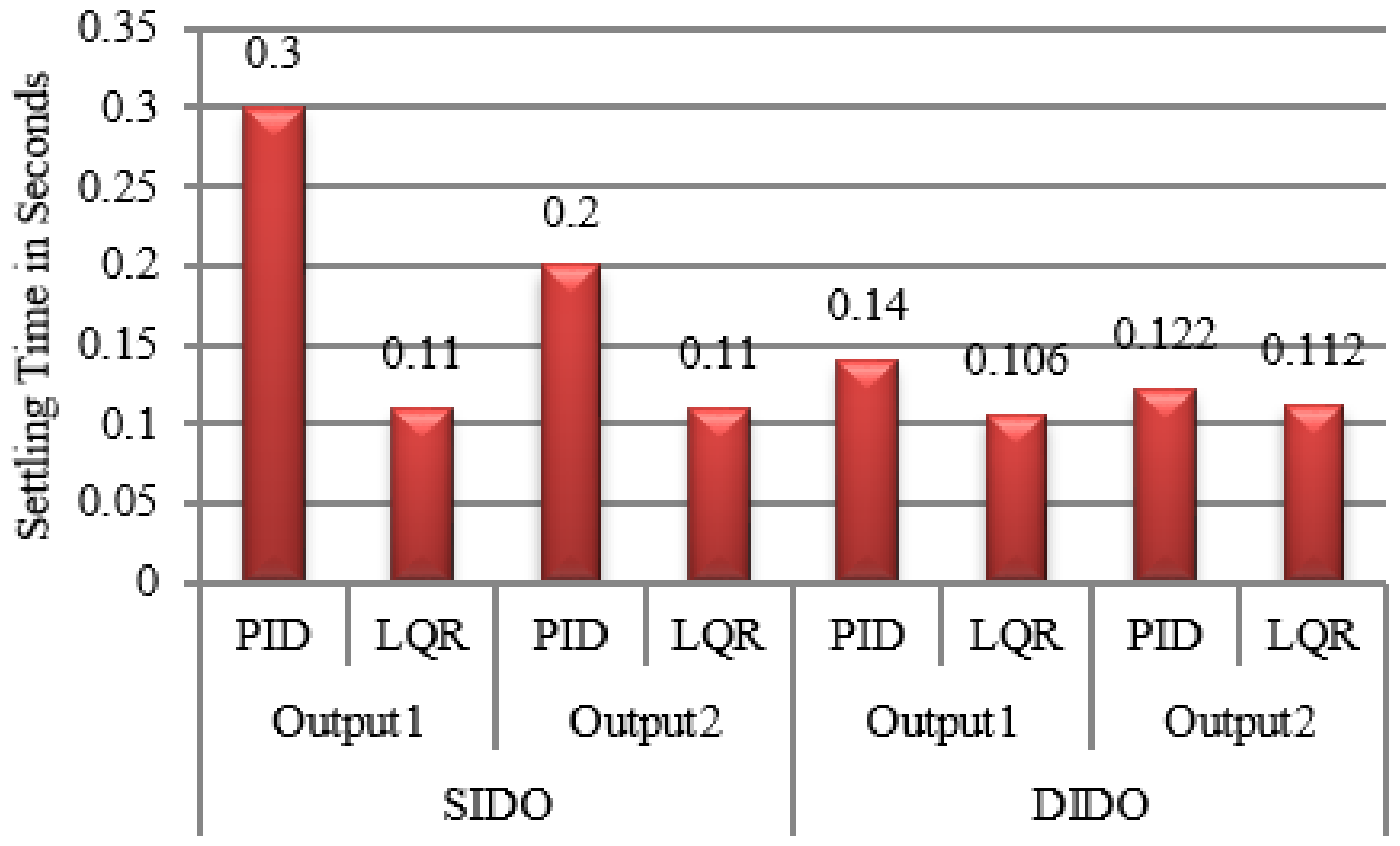
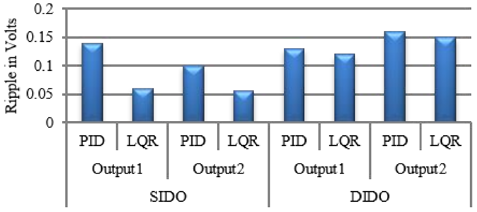
8. Performance Comparison
Performance comparison of Multivariable PID and Optimal LQR controllers for SIDO and DIDO are done in terms of Settling Time, Ripples and Cross Regulation.
Table 3 clearly indicates the amount of cross regulation in output 2 when load disturbance is given at output 1 and proves that LQR controller performs well for both the converters.
Figure 14 and
Figure 15 show the bar graph which indicates the settling time and ripple of both the converters respectively when both multivariable PID and LQR controllers are used at the operating point.
The graph clearly says that settling time is comparatively less when LQR controller is used at the desired operating point.
From
Figure 15, it is clearly found that the ripples are low for LQR.
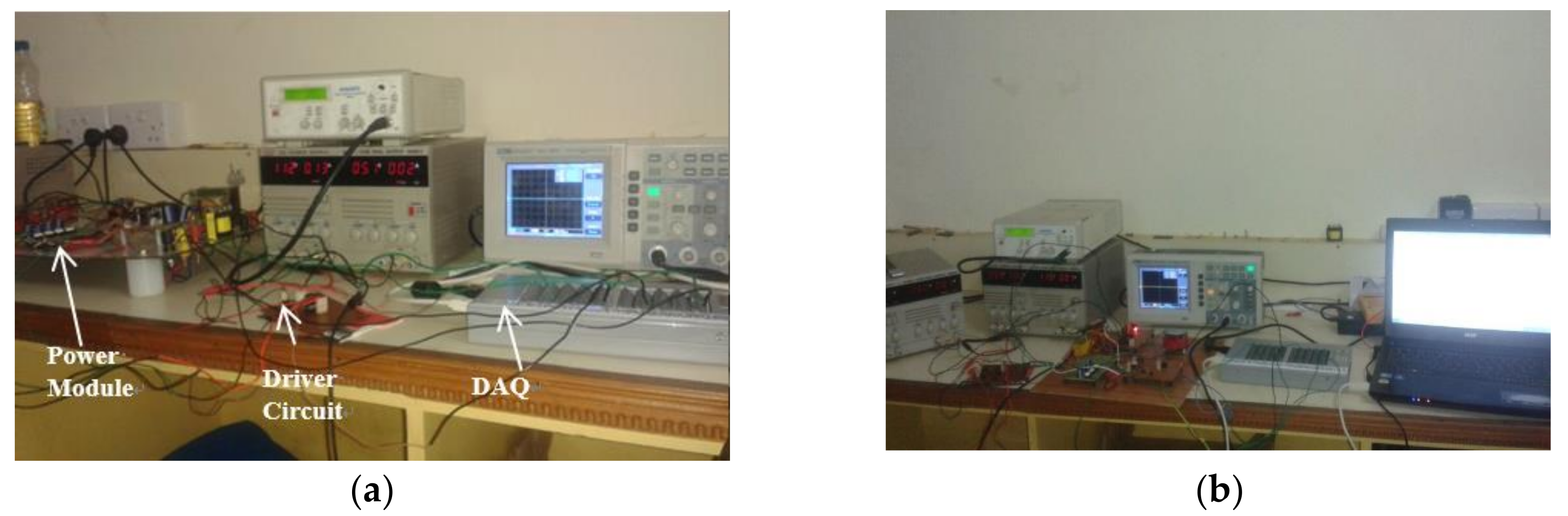
Table 3 clearly indicates that the cross regulation between the outputs is reduced for LQR controller. In terms of peak overshoot, the output voltages have less amount of peak overshoot when LQR controller is used. As the LQR controller performs well for both the converters in terms of settling time, ripple and cross regulation, the simulated results are validated with the help of DAQ module.
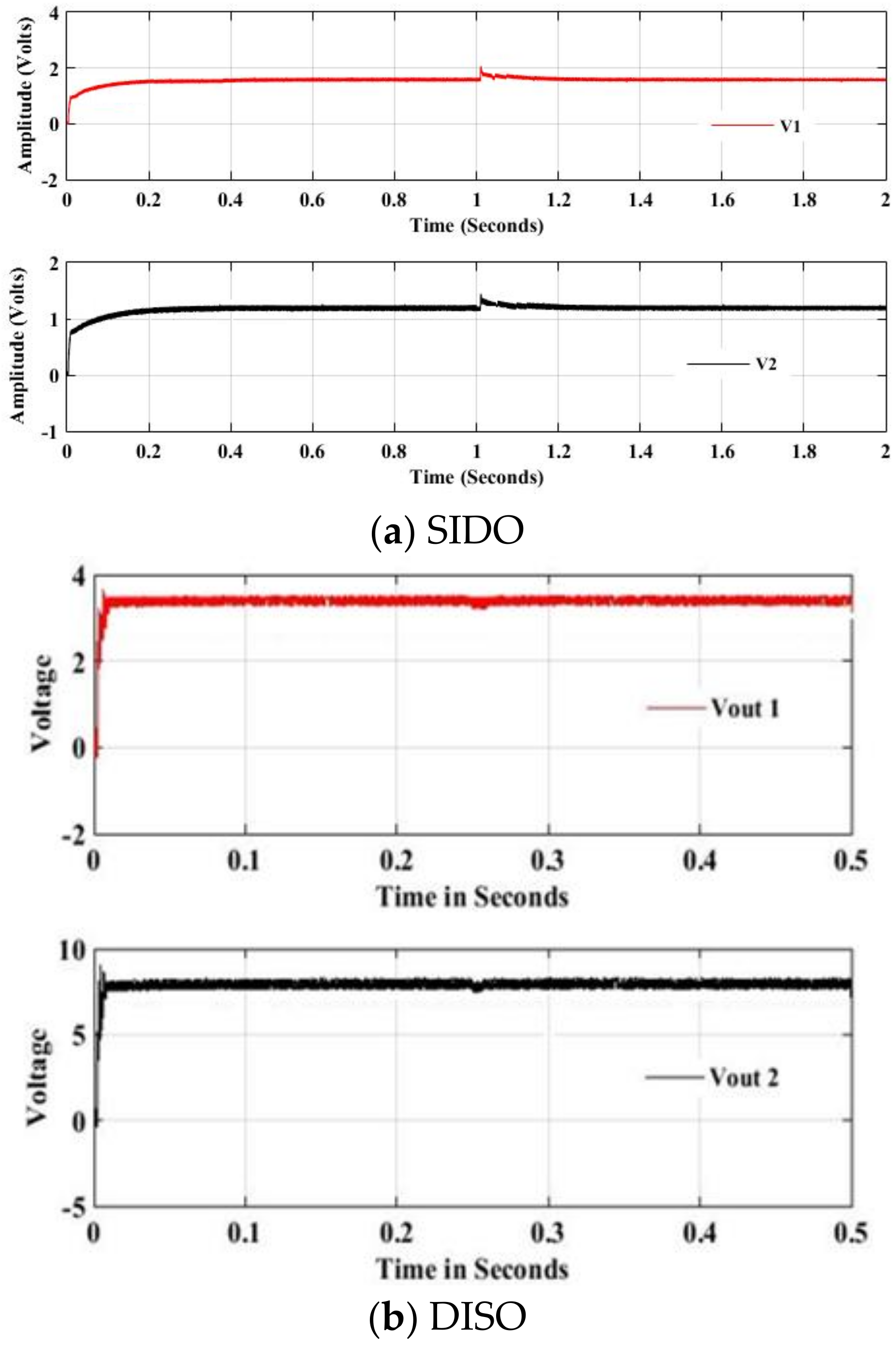
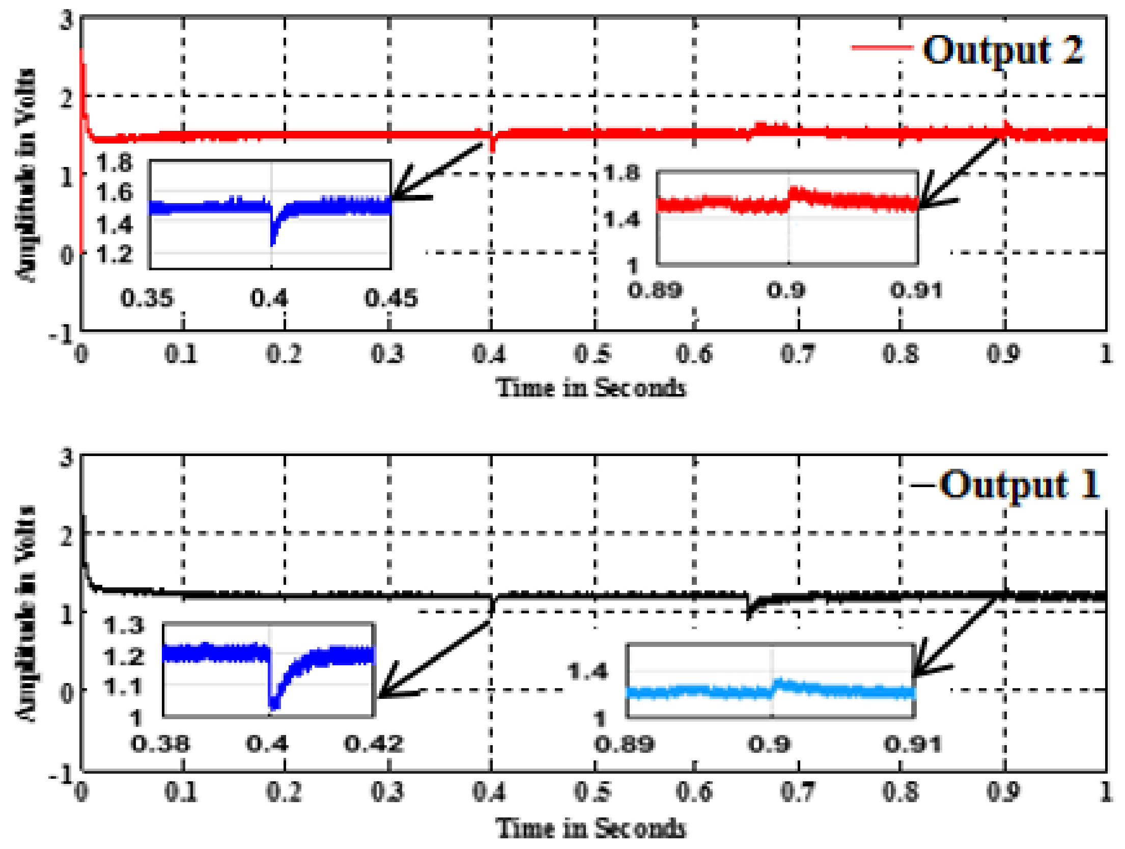
Figure 16a,b show the validation of the simulated results with the prototype model of the converters using DAQ module.
Figure 16a clearly shows that the output voltages have very good transient responses and minimal cross regulation of 0.1 V increase at output 2 when load disturbance is given at
t = 1 s in output 1 and comes back to the operating point within a time period of fewer than 5 milliseconds. The
Figure 16b reveals that the simulation results of the DIDO converter with LQR controller in
Figure 13 is validated.
Figure 17 shows the Gershgorin bands of the transfer function matrix with LQR optimal controllers.
It is found that the system is diagonal dominance as the bands have become narrower and moreover the system has become stable at all frequencies. Again, RGA is used as a parameter to measure the inputs and outputs interactions. RGA for both the systems is given in Equation (50):
As the RGA matrix for both the systems is diagonal, the system has become decoupled due to the addition of a controller. This implies that the cross regulation is minimized using LQR controller.


