Partial Discharge Analysis under High-Frequency, Fast-Rise Square Wave Voltages in Silicone Gel: A Modeling Approach


Abstract
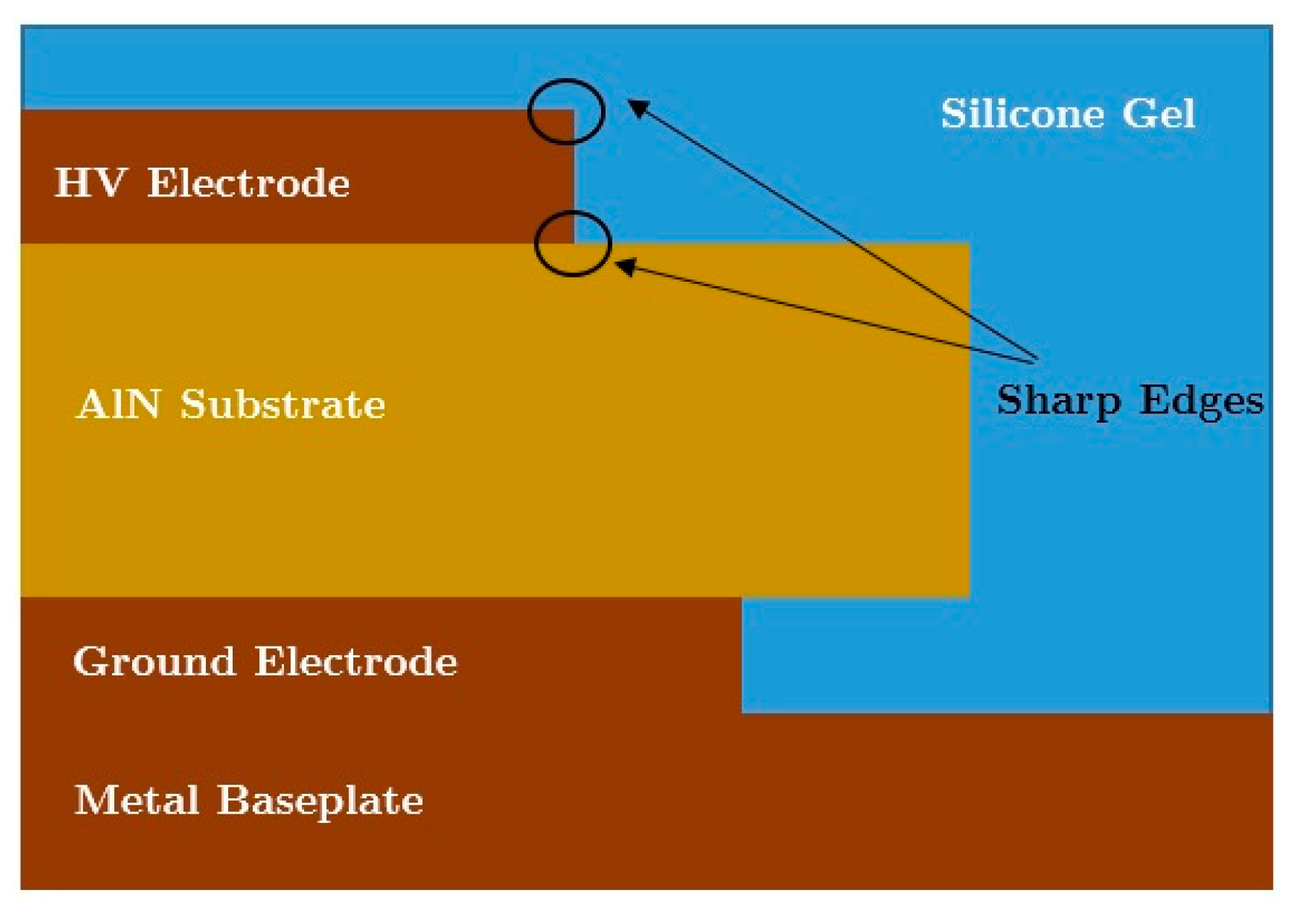
:1. Introduction
2. PD Initiation and Propagation
2.1. Streamer Inception Criterion
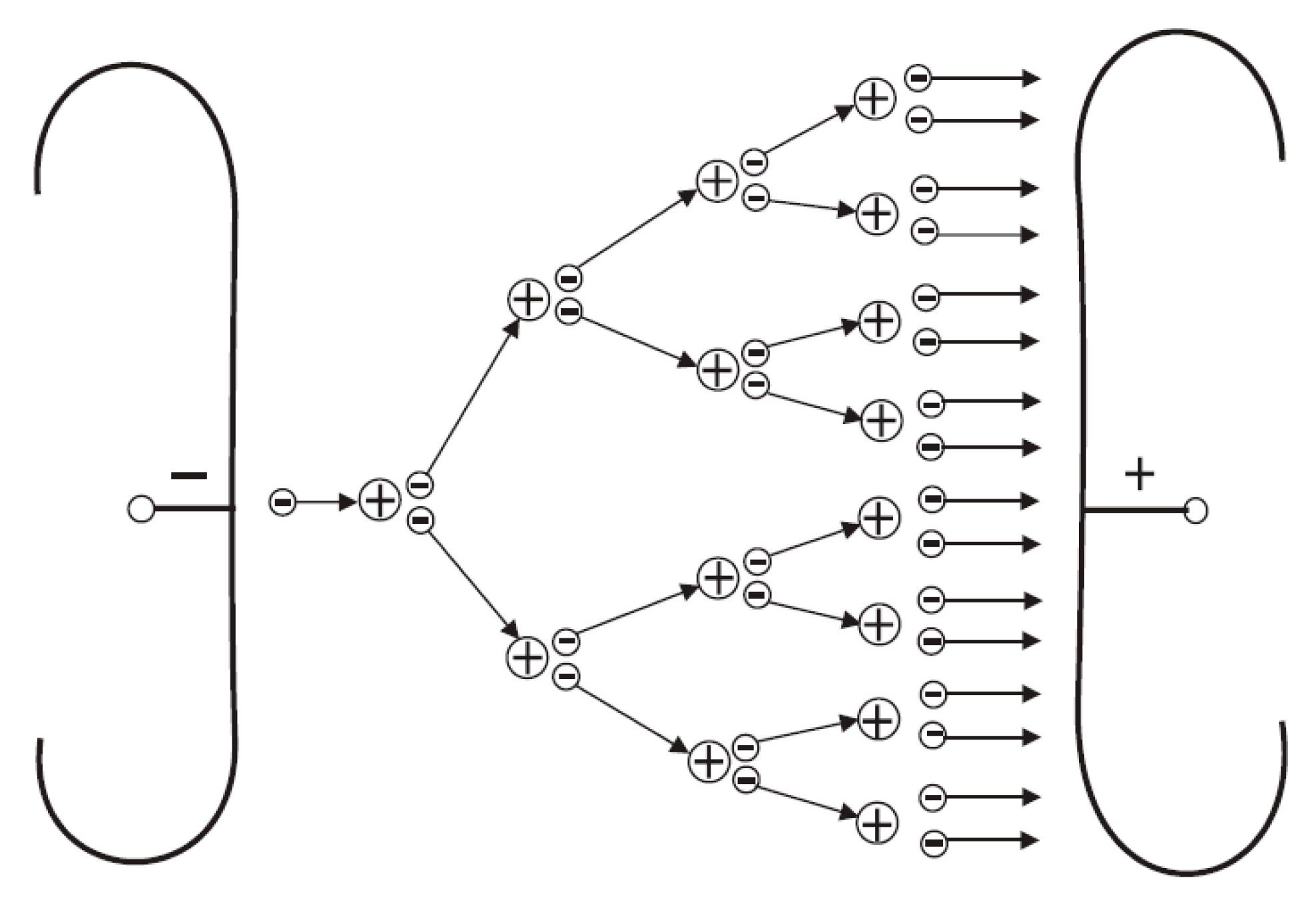
2.2. Initial Free-Electron
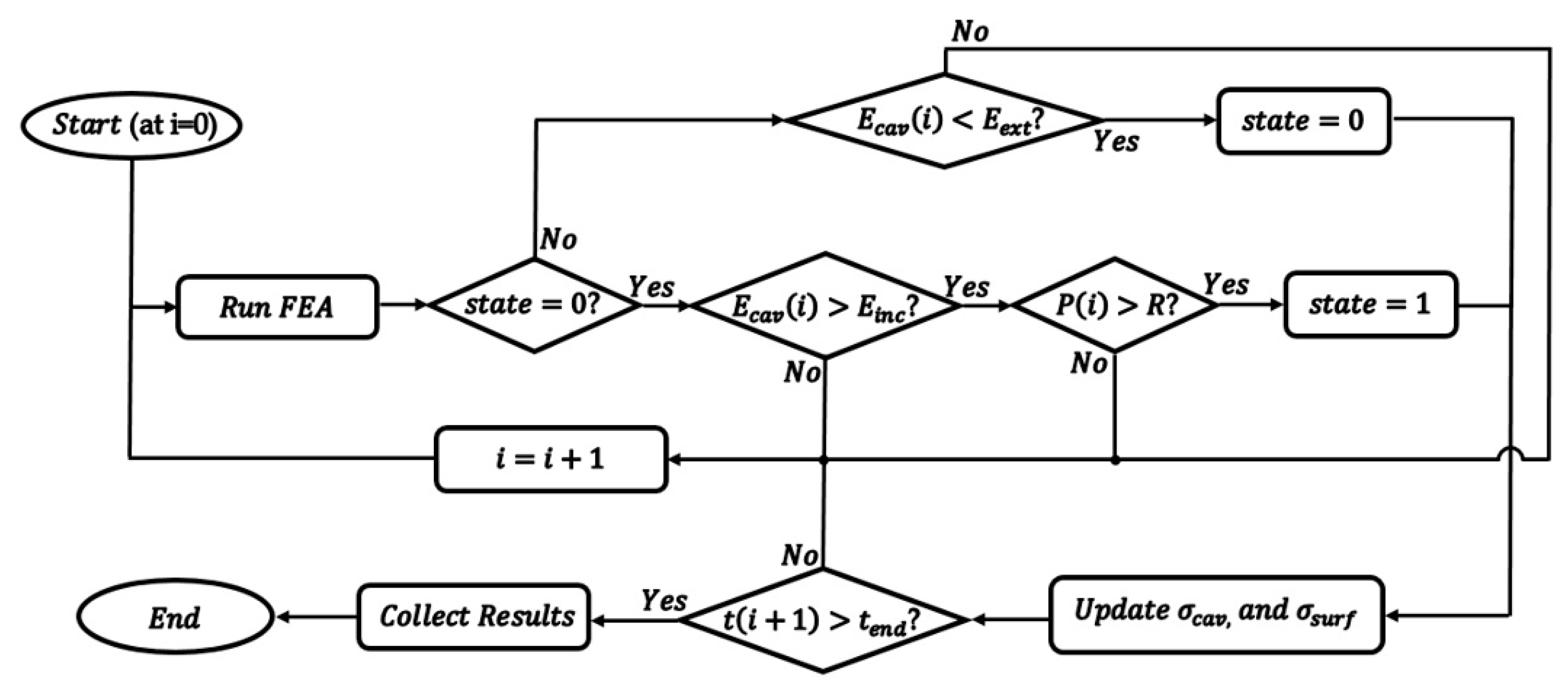
3. Modeling of the PD Process
4. Results and Key Challenges
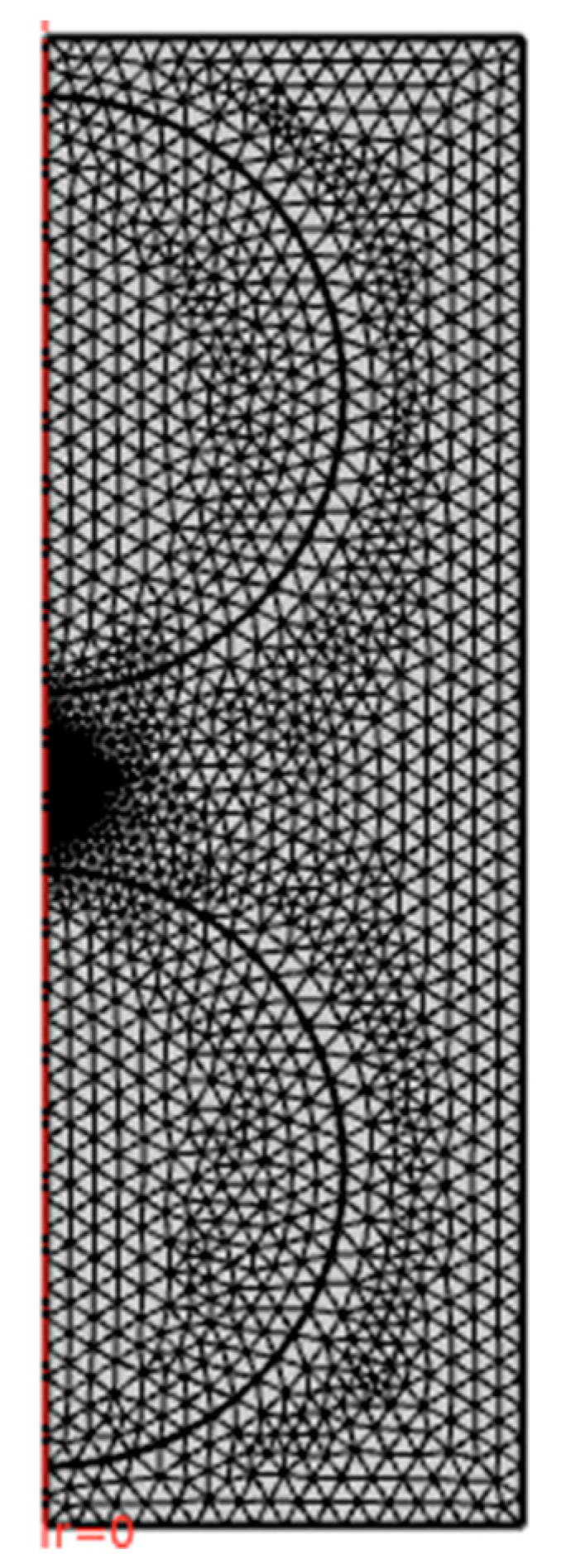
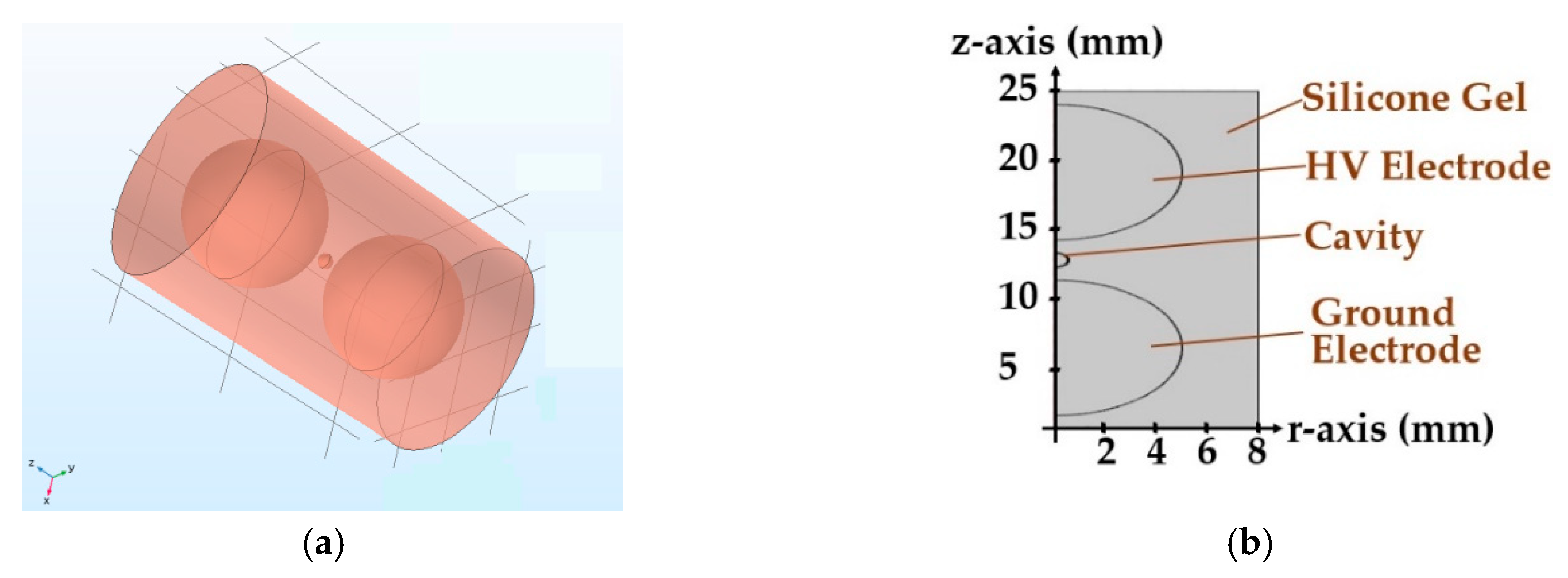
4.1. Case Study
4.2. Results
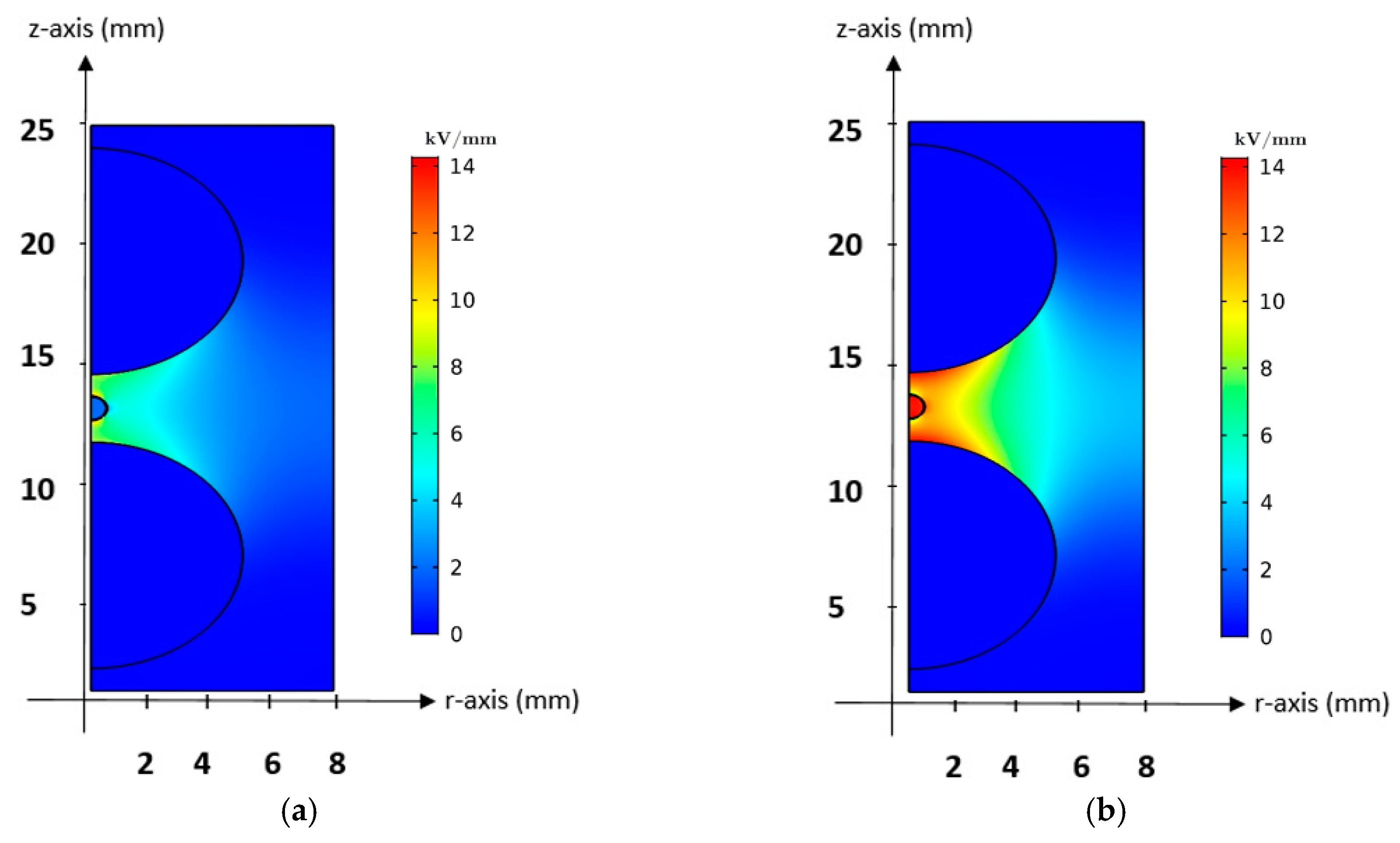
4.2.1. Field Distribution before and after PD
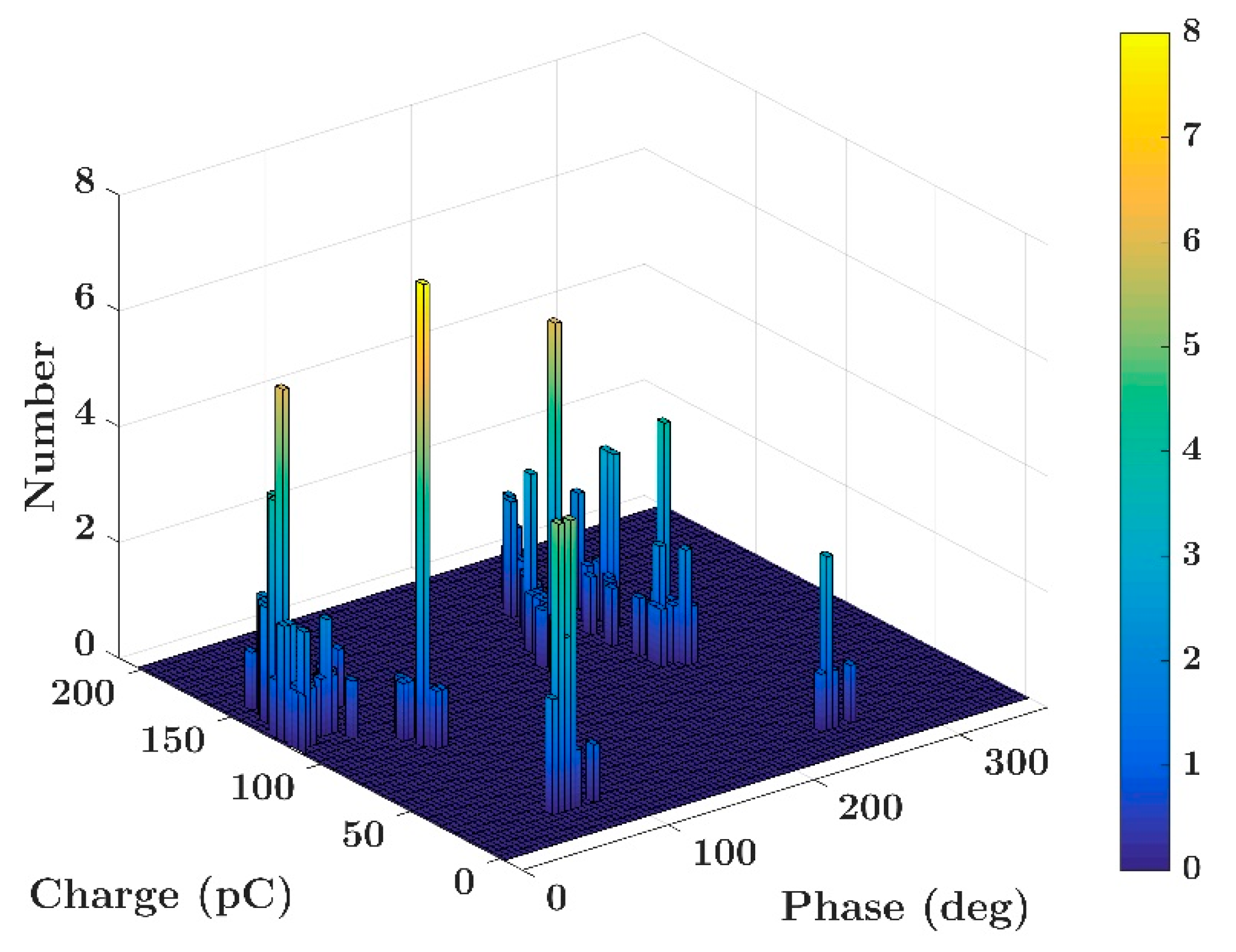
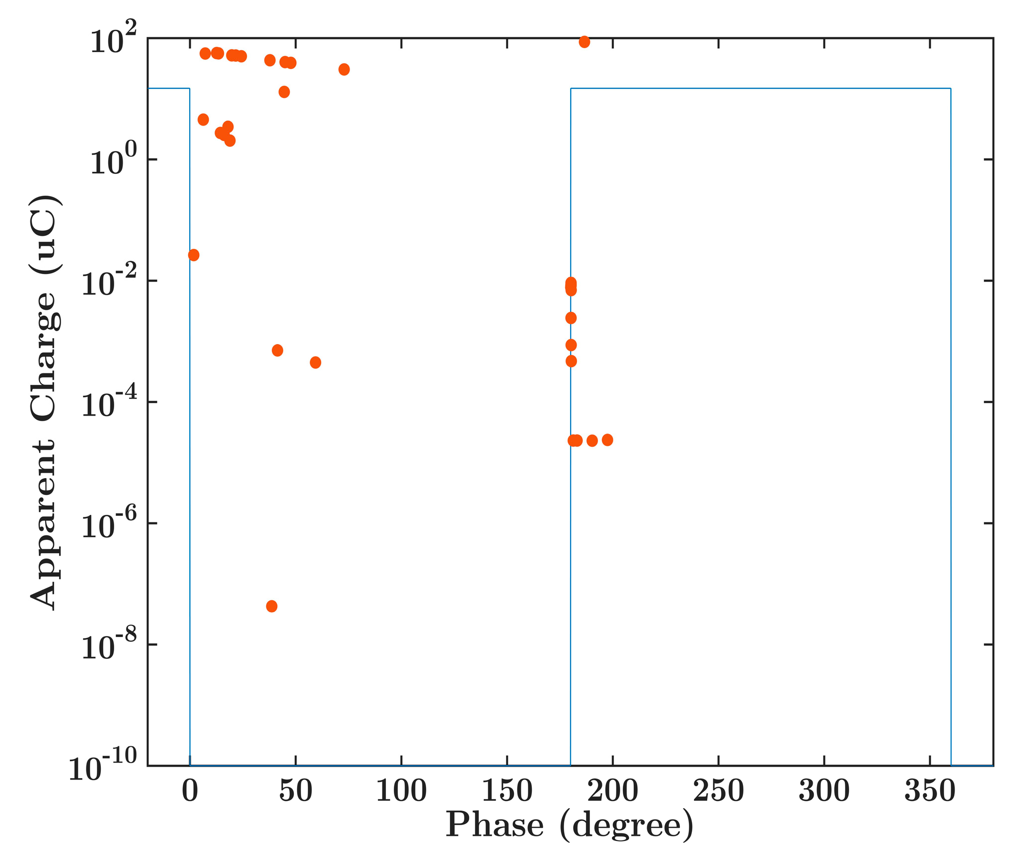
4.2.2. Discharge Pulses over Time for 20 Cycles
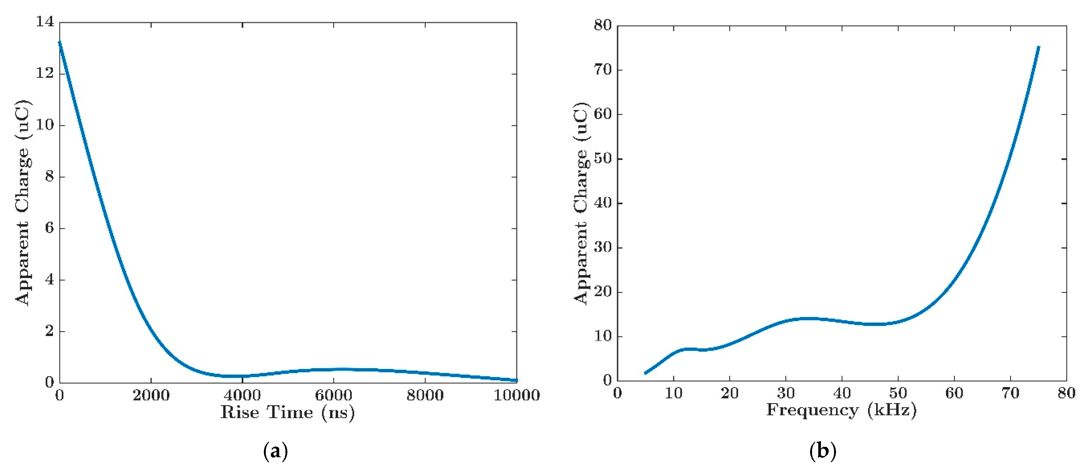
4.2.3. Rise-Time and Frequency Impact
4.3. Key Challenges
4.3.1. Estimation of Model Parameters
4.3.2. Convergence Problem
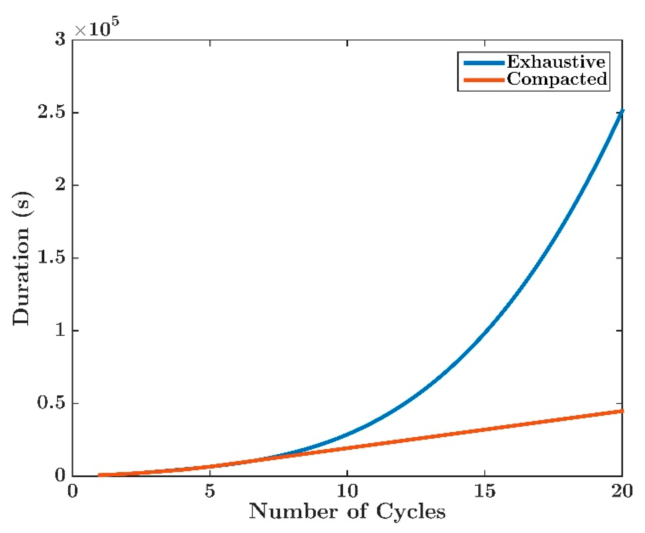
4.3.3. Burden of Calculation
5. Conclusions
Author Contributions
Funding
Conflicts of Interest
References
- Passmore, B.; O’Neal, C. High-Voltage SiC Power Modules for 10–25 kV Applications. Power Electron. Europe Mag. 2016, 1, 22–24. [Google Scholar]
- Ghassemi, M. PD Measurements, Failure Analysis, and Control in High-Power IGBT Modules. High Volt. 2018, 3, 170–178. [Google Scholar] [CrossRef]
- Ghassemi, M. Electrical Insulation Weaknesses in Wide Bandgap Devices. In Simulation and Modelling of Electrical Insulation Weaknesses in Electrical Equipment; Albarracin, R., Ed.; IntechOpen: London, UK, 2018; pp. 129–149. [Google Scholar]
- Ghassemi, M. Accelerated Insulation Aging Due to Fast, Repetitive Voltages: A Review Identifying Challenges and Future Research Needs. IEEE Trans. Dielectr. Electr. Insul. 2019, 26, 1558–1568. [Google Scholar] [CrossRef]
- Mancinelli, P.; Cavallini, A.; Dodd, S.J.; Chalashkanov, N.M.; Dissado, L.A. Analysis of Electrical Tree Inception in Silicone Gels. IEEE Trans. Dielectr. Electr. Insul. 2017, 24, 3974–3984. [Google Scholar] [CrossRef]
- Madonia, A.; Romano, P.; Hammarström, T.; Gubanski, S.M.; Viola, F.; Imburgia, A. PD characteristics at square shaped voltages applying two different detecting techniques. In Proceedings of the IEEE Conference on Electrical Insulation and Dielectric Phenomena (CEIDP), Toronto, ON, Canada, 16–19 October 2016; pp. 247–250. [Google Scholar]
- Hammarström, T.J.Å. Partial Discharge Characteristics at Ultra-Short Voltage Rise Times. IEEE Trans. Dielectr. Electr. Insul. 2018, 25, 2241–2249. [Google Scholar] [CrossRef]
- Dodd, S.J.; Salvatierra, L.; Dissado, L.A.; Mola, E. Electrical trees in silicone gel: A combination of liquid and solid behaviour patterns. In Proceedings of the IEEE Conference on Electrical Insulation and Dielectric Phenomena (CEIDP), Shenzhen, China, 20–23 October 2016; pp. 1018–1021. [Google Scholar]
- Sato, M.; Kumada, A.; Hidaka, K.; Yamashiro, K.; Hayase, Y.; Takano, T. Degradation process of silicone-gel by internal surface discharges. In Proceedings of the IEEE International Conference on Dielectric Liquids (ICDL), Bled, Slovenia, 29 June–3 July 2014; pp. 1–4. [Google Scholar]
- Wang, N.; Cotton, I.; Robertson, J.; Follmann, S.; Evans, K.; Newcombe, D. Partial Discharge Control in a Power Electronic Module Using High Permittivity Non-Linear Dielectrics. IEEE Trans. Dielectr. Electr. Insul. 2010, 17, 1319–1326. [Google Scholar] [CrossRef]
- Niemeyer, L. A Generalized Approach to Partial Discharge Modeling. IEEE Trans. Dielectr. Electr. Insul. 1995, 2, 510–528. [Google Scholar] [CrossRef]
- Ghassemi, M. Geometrical techniques for electric field control in (ultra) wide bandgap power electronics modules. In Proceedings of the IEEE Electrical Insulation Conference (EIC), San Antonio, TX, USA, 17–20 June 2018; pp. 589–592. [Google Scholar]
- Tousi, M.M.; Ghassemi, M. Electric field control by nonlinear field dependent conductivity dielectrics characterization for high voltage power module packaging. In Proceedings of the IEEE International Workshop on Integrated Power Packaging (IWIPP), Toulouse, France, 24–26 April 2019; pp. 54–58. [Google Scholar]
- Tousi, M.M.; Ghassemi, M. Nonlinear field dependent conductivity materials for electric field control within next-generation wide bandgap power electronics modules. In Proceedings of the 2019 IEEE Electrical Insulation Conference (EIC), Calgary, AB, Canada, 16–19 June 2019; pp. 63–66. [Google Scholar]
- Tousi, M.M.; Ghassemi, M. Electrical insulation packaging for a 20 kV high density wide bandgap power module. In Proceedings of the IEEE Energy Conversion Congress & Exposition (ECCE), Baltimore, MD, USA, 29 September–3 October 2019; pp. 4162–4166. [Google Scholar]
- Tousi, M.M.; Ghassemi, M. Nonlinear resistive electric field grading in high-voltage, high-power wide bandgap power module packaging. In Proceedings of the IEEE Energy Conversion Congress & Exposition (ECCE), Baltimore, MD, USA, 29 September–3 October 2019; pp. 7124–7129. [Google Scholar]
- Tousi, M.M.; Ghassemi, M. The effect of type of voltage (sinusoidal and square waveform) and the frequency on the performance of nonlinear field-dependent conductivity coatings for electric field control in power electronic modules. In Proceedings of the IEEE Conference on Electrical Insulation and Dielectric Phenomena (CEIDP), Richland, DC, USA, 20–23 October 2019; pp. 601–604. [Google Scholar]
- Tousi, M.M.; Ghassemi, M. Combined Geometrical Techniques and Applying Nonlinear Field Dependent Conductivity Layers to Address the High Electric Field Stress Issue in High Voltage High-Density Wide Bandgap Power Modules. IEEE Trans. Dielectr. Electr. Insul. 2019, in press. [Google Scholar]
- Tousi, M.M.; Ghassemi, M. Characterization of Nonlinear Field Dependent Conductivity Layer Coupled with Protruding Substrate to Address High Electric Field Issue within High Voltage High-Density Wide Bandgap Power Modules. IEEE J. Emerg. Sel. Top. Power Electron. 2019, in press. [Google Scholar] [CrossRef]
- Whitehead, S. Dielectric Breakdown in Solids; Clarendon Press: Oxford, UK, 1951. [Google Scholar]
- Crichton, G.C.; Karlsson, P.W.; Pedersen, A. Partial Discharges in Ellipsoidal and Spheroidal Voids. IEEE Trans. Electr. Insul. 1989, 24, 335–342. [Google Scholar] [CrossRef]
- Pedersen, A.; Crichton, G.C.; McAllister, I.W. The Theory and Measurement of Partial Discharge Transients. IEEE Trans. Electr. Insul. 1991, 26, 487–497. [Google Scholar] [CrossRef]
- Pedersen, A.; Crichton, G.C.; McAllister, I.W. The Functional Relation Between Partial Discharges and Induced Charge. IEEE Trans. Dielectr. Electr. Insul. 1995, 2, 535–543. [Google Scholar] [CrossRef]
- Gutfleisch, F.; Niemeyer, L. Measurement and Simulation of PD in Epoxy Voids. IEEE Trans. Dielectr. Electr. Insul. 1995, 2, 729–743. [Google Scholar] [CrossRef]
- Achillides, Z.; Danikas, M.G.; Kyriakides, E. Partial Discharge Modeling and Induced Charge Concept: Comments and Criticism of Pedersen’s Model and Associated Measured Transients. IEEE Trans. Dielectr. Electr. Insul. 2017, 24, 1118–1122. [Google Scholar] [CrossRef]
- Achillides, Z.; Kyriakides, E.; Georghiou, G.E. Partial Discharge Modeling: An Improved Capacitive Model and Associated Transients along Medium Voltage Distribution Cables. IEEE Trans. Dielectr. Electr. Insul. 2013, 20, 770–781. [Google Scholar] [CrossRef]
- Finis, G.; Claudi, A. On the Dielectric Breakdown Behavior of Silicone Gel Under Various Stress Conditions. IEEE Trans. Dielectr. Electr. Insul. 2007, 14, 487–494. [Google Scholar] [CrossRef]
- Schifani, R.; Candela, R.; Romano, P. On PD Mechanisms at High Temperature in Voids Included in an Epoxy Resin. IEEE Trans. Dielectr. Electr. Insul. 2001, 8, 589–597. [Google Scholar] [CrossRef]
- Illias, H.; Chen, G.; Lewin, P.L. Partial Discharge Behavior Within a Spherical Cavity in a Solid Dielectric Material as a Function of Frequency and Amplitude of the Applied Voltage. IEEE Trans. Dielectr. Electr. Insul. 2011, 18, 432–443. [Google Scholar] [CrossRef]
- Forssen, C. Partial Discharges in Cylindrical Cavities at Variable Frequency of the Applied Voltage. Licentiate’s Thesis, KTH Royal Institute of Technology, Stockholm, Sweden, 2005. [Google Scholar]
- Borghei, M.; Ghassemi, M. Finite element modeling of partial discharge activity within a spherical cavity in a solid dielectric material under fast, repetitive voltage pulses. In Proceedings of the IEEE Electrical Insulation Conference (EIC), Calgary, AB, Canada, 16–19 June 2019; pp. 34–37. [Google Scholar]
- Borghei, M.; Ghassemi, M. Partial discharge finite element analysis under fast, repetitive voltage pulses. In Proceedings of the IEEE Electric Ship Technologies Symposium (ESTS), Arlington, VA, USA, 13–19 August 2019; pp. 324–328. [Google Scholar]
- Borghei, M.; Ghassemi, M.; Rodriguez-Serna, J.M.; Albarracin Sanchez, R. Finite Element Analysis and Induced Charge Concept Methods for Internal Partial Discharge Modeling: A Comparison. IEEE Trans. Dielectr. Electr. Insul. 2019, in press. [Google Scholar]
- Wang, P.; Cavallini, A.; Montanari, G.C. The Influence of Repetitive Square Wave Voltage Parameters on Enameled Wire Endurance. IEEE Trans. Dielectr. Electr. Insul. 2014, 21, 1276–1284. [Google Scholar] [CrossRef]
- Ebke, T.; Khaddour, A.; Peier, D. Degradation of silicone gel by partial discharges due to different defects. In Proceedings of the International Conference on Dielectric Materials, Measurements and Applications, Edinburgh, UK, 17–21 September 2000; pp. 202–207. [Google Scholar]
- Chung, J.; Hulbert, G.M. A Time Integration Algorithm for Structural Dynamics with Improved Numerical Dissipation: The Generalized-α Method. J. Appl. Mech. 1993, 60, 371–375. [Google Scholar] [CrossRef]


| Symbol | Parameter | Value |
|---|---|---|
| Geometrical | ||
| cavity diameter | ||
| electrode radius | ||
| distance between electrodes | ||
| Silicone gel relative permittivity | ||
| conductivity | ||
| Applied Voltage voltage peak magnitude | ||
| frequency | ||
| rise-time | ||
| duty cycle |
| Symbol | Value |
|---|---|
| Quantity | Value |
|---|---|
| Maximum element size | |
| Minimum element size | |
| Maximum element growth rate | |
| Curvature factor | |
| Resolution of narrow regions | |
| Maximum element size |
| Quantity | Value |
|---|---|
| Number of PDs per cycle | 1.9866 |
| Mean duration of PD | |
| Mean true charge | |
| Mean apparent charge | |
| Maximum true charge | |
| Maximum apparent charge |
© 2019 by the authors. Licensee MDPI, Basel, Switzerland. This article is an open access article distributed under the terms and conditions of the Creative Commons Attribution (CC BY) license (http://creativecommons.org/licenses/by/4.0/).
Share and Cite
Borghei, M.; Ghassemi, M. Partial Discharge Analysis under High-Frequency, Fast-Rise Square Wave Voltages in Silicone Gel: A Modeling Approach. Energies 2019, 12, 4543. https://doi.org/10.3390/en12234543
Borghei M, Ghassemi M. Partial Discharge Analysis under High-Frequency, Fast-Rise Square Wave Voltages in Silicone Gel: A Modeling Approach. Energies. 2019; 12(23):4543. https://doi.org/10.3390/en12234543
Chicago/Turabian StyleBorghei, Moein, and Mona Ghassemi. 2019. "Partial Discharge Analysis under High-Frequency, Fast-Rise Square Wave Voltages in Silicone Gel: A Modeling Approach" Energies 12, no. 23: 4543. https://doi.org/10.3390/en12234543
APA StyleBorghei, M., & Ghassemi, M. (2019). Partial Discharge Analysis under High-Frequency, Fast-Rise Square Wave Voltages in Silicone Gel: A Modeling Approach. Energies, 12(23), 4543. https://doi.org/10.3390/en12234543