Article

Sliding Mode Based Control of Dual Boost Inverter for Grid Connection

by
Diana Lopez-Caiza
1,*,†,
Freddy Flores-Bahamonde
1,†,
Samir Kouro
1,†,
Victor Santana
2,†,
Nicolás Müller
1,† and
Andrii Chub
3,†
1
Electronics Engineering Department, Universidad Técnica Federico Santa María, Valparaíso 2390123, Chile
2
Advanced Center for Electrical and Electronic Engineering, Valparaíso 2390212, Chile
3
Department of Electrical Power Engineering and Mechatronics, Tallinn University of Technology, 19086 Tallinn, Estonia
*
Author to whom correspondence should be addressed.
These authors contributed equally to this work.
Energies 2019, 12(22), 4241; https://doi.org/10.3390/en12224241
Submission received: 27 September 2019 / Revised: 30 October 2019 / Accepted: 4 November 2019 / Published: 7 November 2019
(This article belongs to the Special Issue Sliding Mode Control of Power Converters in Renewable Energy Systems)

Abstract

:
Single-stage voltage step-up inverters, such as the Dual Boost Inverter (DBI), have a large operating range imposed by the high step-up voltage ratio, which together with the converter of non-linearities, makes them a challenge to control. This is particularly the case for grid-connected applications, where several cascaded and independent control loops are necessary for each converter of the DBI. This paper presents a global current control method based on a combination of a linear proportional resonant controller and a non-linear sliding mode controller that simplifies the controller design and implementation. The proposed control method is validated using a grid-connected laboratory prototype. Experimental results show the correct performance of the controller and compliance with power quality standards.

Graphical Abstract

1. Introduction

Two-stage power converters are generally used for connecting low-voltage DC sources, such as photovoltaic modules, batteries, fuel cells, and super-capacitors, to AC grids. The input voltage is boosted beyond the peak voltage of the grid by the first stage, a DC–DC converter, which is then converted to AC by the second stage, the grid–tie inverter [1]. However, the efficiency of a two-stage conversion system, particularly when a high step-up voltage DC–DC stage is required, is the main disadvantage of such configuration. The size, cost, and reliability are also factors to take into account in two-stage conversion systems. In this context, single-stage power converters have been proposed to improve the overall efficiency, by reducing the numbers of elements in the system. One of these topologies is the Dual Boost Inverter (DBI) originally introduced in [2].
The DBI consists of two bidirectional DC–DC boost converters, connected in parallel at the DC input and differential mode at the AC output. To obtain a sinusoidal output voltage, each DC–DC boost converter generates a sinusoidal output (with opposite phase between each other), relative to a substantial DC-bias (equal for both converters) which is canceled through the differential connection, leaving only the AC component at the output. Thus, each converter works around an operating point (the DC-bias) but with a large variable output voltage range (the AC component). Additionally, the product between the control and state variables, present in the averaged model of the DC–DC boost converter, shows the high non-linearity of the system [3]. Consequently, the main challenge of DBI is in design of a control system.
From the introduction of the DBI, several control techniques have been proposed in the literature, which can be classified into two main groups of control strategies: independent and global. In the first group, each boost converter is controlled individually to generate its respective sinusoidal output voltage employing linear and non-linear methods. In most cases, a cascaded linear control scheme is used, with a slower outer control loop for the capacitor voltage, and a faster (higher bandwidth) control loop for inductor current. Examples of this control strategy can be found in [4,5,6], where proportional-integral (PI) controllers are employed in both loops. However, PI controllers can lead to steady-state errors and phase shifts when used to control sinusoidal signals. For this reason, proportional resonant (PR) controllers have been proposed in [7,8], as an alternative to overcome these issues. One common condition for these control strategies is to ensure that the minimum DC-bias is composed of the input DC voltage and half of the amplitude of the output AC voltage to achieve the proper operation of each DC–DC converter.
Also, some non-linear techniques can be found in the group of independent control strategies. Among them: sliding mode control, with a switching surface composed by the error in the voltage of the capacitor and the inductor current is presented in [9]; a dynamic linearizing modulator used to control the capacitor voltage is presented in [10]; the differential flatness propriety, as shown in [11], where the individual control of the output voltage is indirectly accomplished through the regulation of energy stored in each boost converter; and finite control set model predictive control, where a non-linear discrete model of the DBI is used to predict and optimize the behavior of each converter, as introduced in [12].
In contrast, in the global control strategy group, the differential output AC voltage of the DBI is considered to be the main control objective. This type of control was introduced for the first time in [3], where a cascaded control diagram based on the sliding mode approach is applied to achieve the sinusoidal output voltage. The external control loop regulates the output voltage error of the inverter using a PI controller. The inner control loop corresponds to a switching surface, synthesized from the difference between the current of the inductors and the external controller output. One advantage of this strategy is the reduction of control loops, which leads to a decrease in the number of required sensors. An extended analysis of the equilibrium point for this control strategy is presented in [13], where the DC component of the capacitor voltages is automatically adjusted to the two-fold of the input voltage.
In most cases, the control strategies have been tested for passive loads (R and R L loads). Although good performances under perturbations have been achieved, the grid connection has not been thoroughly analyzed. This is mainly because it is difficult to find a relationship between the output current and the control variables of the inverter. Nevertheless, experimental validations of grid-connected DBIs can be found in [7,8]. In both cases, the cascaded linear strategy is used to control individually each boost converter, including an additional control loop based on active and reactive power. Therefore, five control loops are necessary to connect the DBI to the grid, making the design and implementation of the control system a complex process. This is particularly an issue for the DBI, which is intended for low power applications, such as grid-connected photovoltaic microinverters, for which low cost control platform are usually used. Other high performance contributions regarding DC–DC converter control have been successfully proposed such as Robust Time-Delay Control for a boost converter [14], as well as adaptive SMC [15], and higher order SMC techniques [16]. However, these have only been proposed for DC–DC converters (not for a DBI with the generation of an AC waveform), and while their extension to current control for DBI may be interesting, they are inherently more complex to implement and require high-end control platforms.
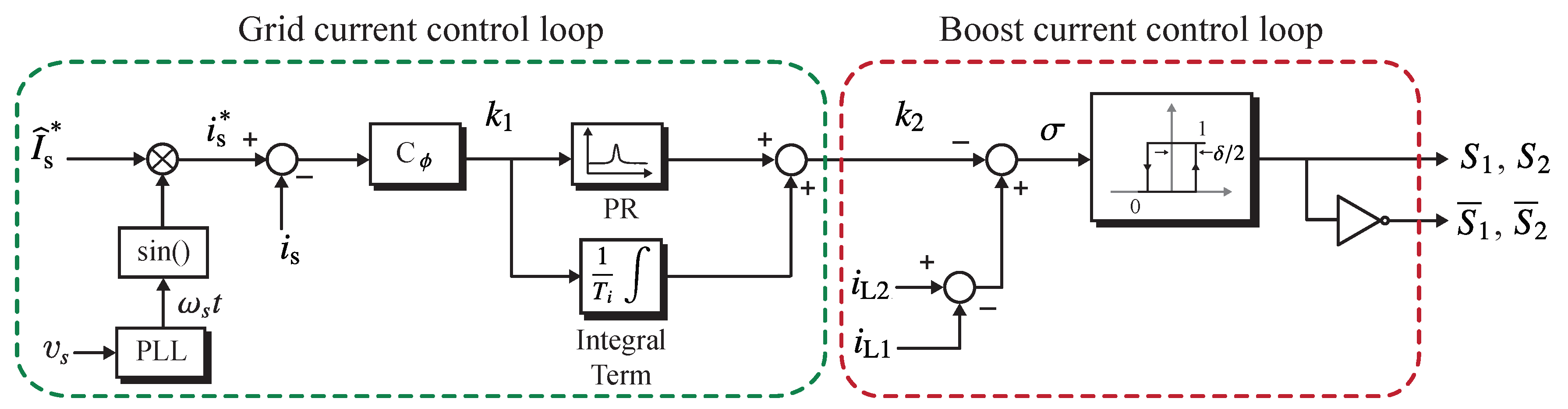
The main contributions of this work are the development of a simple and low computational control system based on SMC with only two control loops. One external linear control loop that regulates the grid current through a PR controller, and an internal non-linear control loop that is composed of a switching surface to control the difference between the current of the DBI inductors. This is feasible due to the symmetry of the DBI allowing the control of both DC–DC converters as a single system by means of a unique control signal, based on an extension of the theoretical derivation of the SMC presented in [13]. However, in this paper the system model and controller derivation has been modified to control the output current instead of voltage. Furthermore, this paper is the first time this principle has been applied to a grid-connected system, with an AC current output, and evaluated experimentally. In addition, experimental performance under grid perturbations and dynamic behavior of the current controller are included. The proposed control system can perform in such circumstances while complying with IEEE standard 1547. The DC-bias achieved by the proposed method is double the input voltage, which is lower than the DC-bias required by traditional methods [4,5,6,7,8], which impacts the size of the capacitors and blocking voltage of the devices.
This paper is organized as follows, a detailed description of the DBI topology is presented in Section 2, the control strategy proposed in this work is introduced in Section 3, the experimental validation and main results of the grid-connected DBI are presented in Section 4, and Section 5 presents the main accomplishments and conclusions of this work.

2. Topology Description

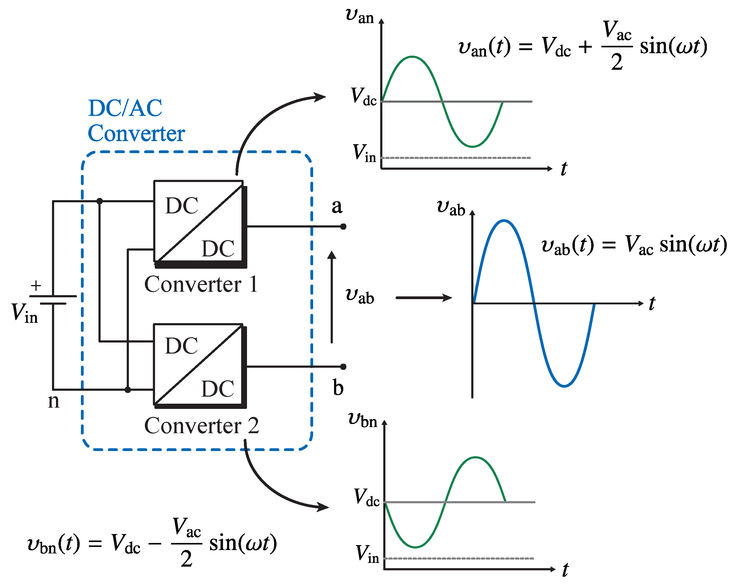
The concept of a generic step-up voltage single-stage differential inverter is shown in Figure 1. The inverter is composed of two bidirectional DC–DC converters, which share the same input source, while their output voltages are connected in differential mode. Each DC–DC converter generates a sinusoidal output voltage with a DC-bias ( V dc ), as shown below
υ an ( t ) = V dc + υ ac ( t ) 2
υ bn ( t ) = V dc υ ac ( t ) 2
The AC component of the output signal of each converter is in the opposite phase regarding the other converter. Thus, considering the same DC component for both converters, the output voltage of the inverter is given by
υ ab ( t ) = υ an ( t ) υ bn ( t ) = V ac · sin ( ω t )
where V ac is the amplitude of the output voltage of the inverter. By generating opposite phase AC signals, the total converter output voltage doubles the individual converter AC amplitude. Therefore, this configuration can achieve a high step-up voltage ratio conversion, one provided by the DC–DC converter boost ratio and one that doubles voltage due to the differential connection. Please note that the DBI fulfills two functions with a single-stage conversion: voltage step-up the DC to AC conversion, to accomplish the grid connection.
In the literature, several bidirectional DC–DC converters have been used, e.g., flyback [17,18], cuk [19,20], and boost [2,3,4,5,6,7,
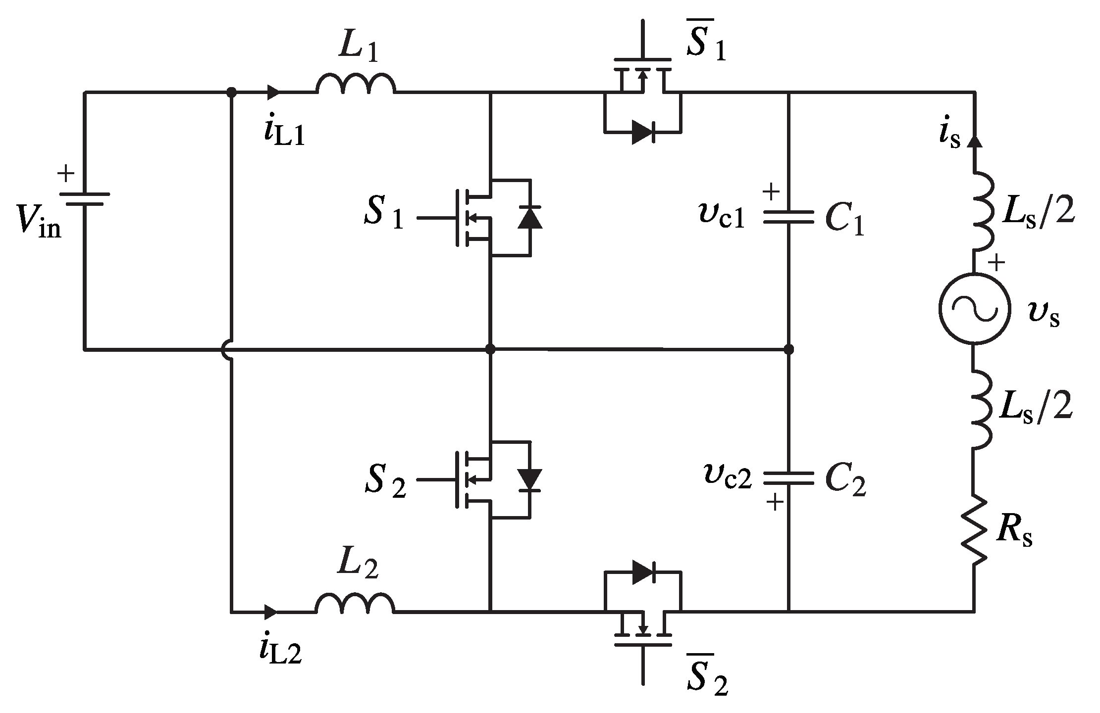
8]. The latter topology, also known as Dual Boost Inverter (DBI), is the one under analysis in this work. The power circuit of the DBI consists of two bidirectional DC–DC boost converters as shown in 
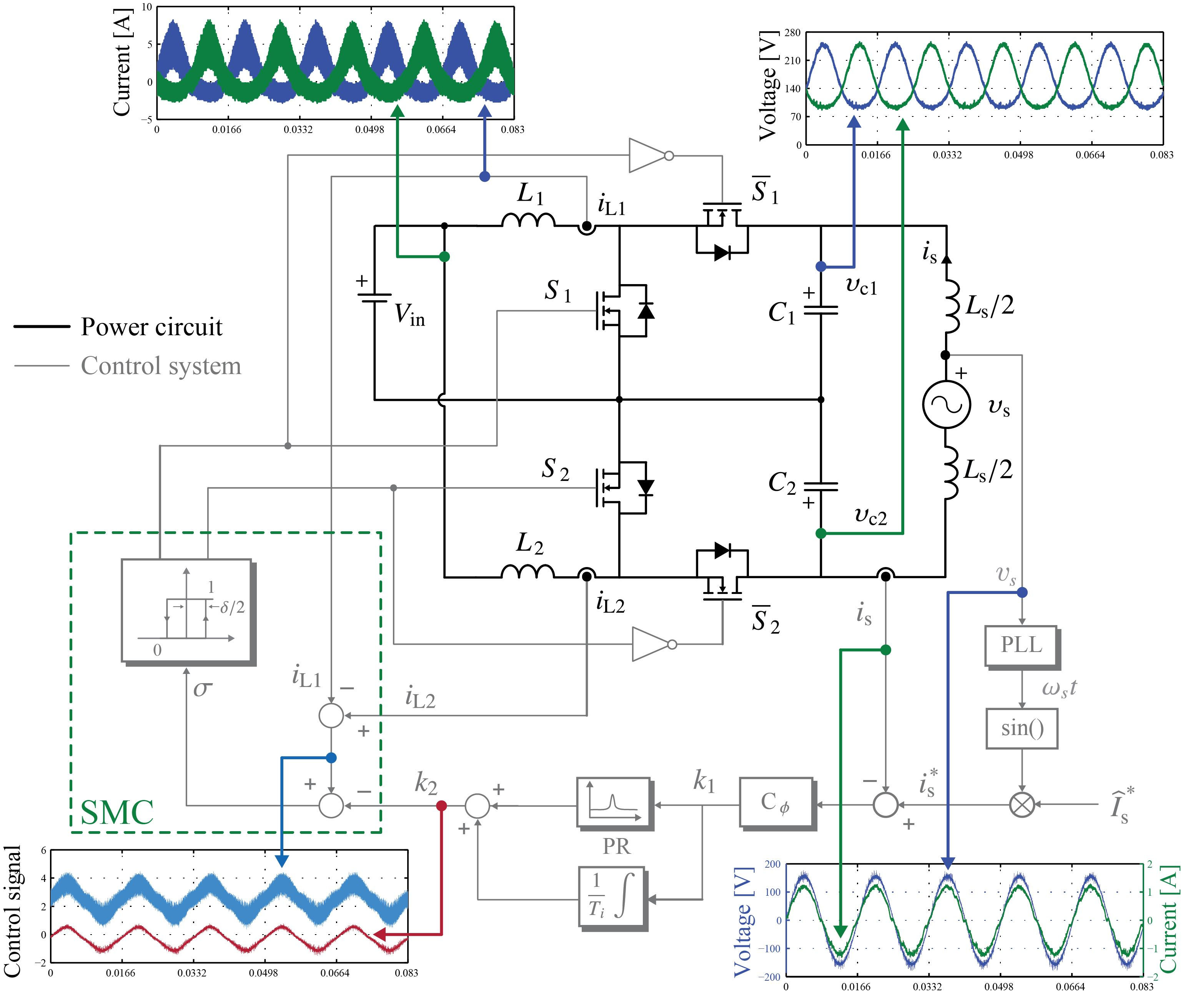
Figure 2 for a grid-connected application. Please note that the outputs of the two DC–DC converters are connected to the grid through a symmetrically divided inductive filter L s . The grid resistance R s is shown for modeling purposes.
To obtain a single averaged switched model of the whole system, two complementary control signals are considered to be in [13], defining the global operation of the system. This idea signifies the difference regarding other works, where the model of the inverter is obtained for each boost converter. Considering the signals u ( t ) = S 1 and 1 u ( t ) = S 2 , the averaged switched model of the DBI is described by
L 1 d i L 1 ( t ) d t = V in υ c 1 ( t ) · ( 1 u ( t ) )
L 2 d i L 2 ( t ) d t = V in υ c 2 ( t ) · u ( t )
C 1 d υ c 1 ( t ) d t = ( 1 u ( t ) ) · i L 1 ( t ) + i s ( t )
C 2 d υ c 2 ( t ) d t = u ( t ) · i L 2 ( t ) i s ( t )
where i L 1 and i L 2 are the currents through the inductors L 1 and L 2 , i s is the grid current, υ c 1 and υ c 2 are the voltage of the capacitors, V in is the input voltage, u ( t ) and 1 u ( t ) are the duty cycles, and S 1 and S 2 are the switching signals.
The product between the state variables and control input (bilinear term) in Equations (4)–(
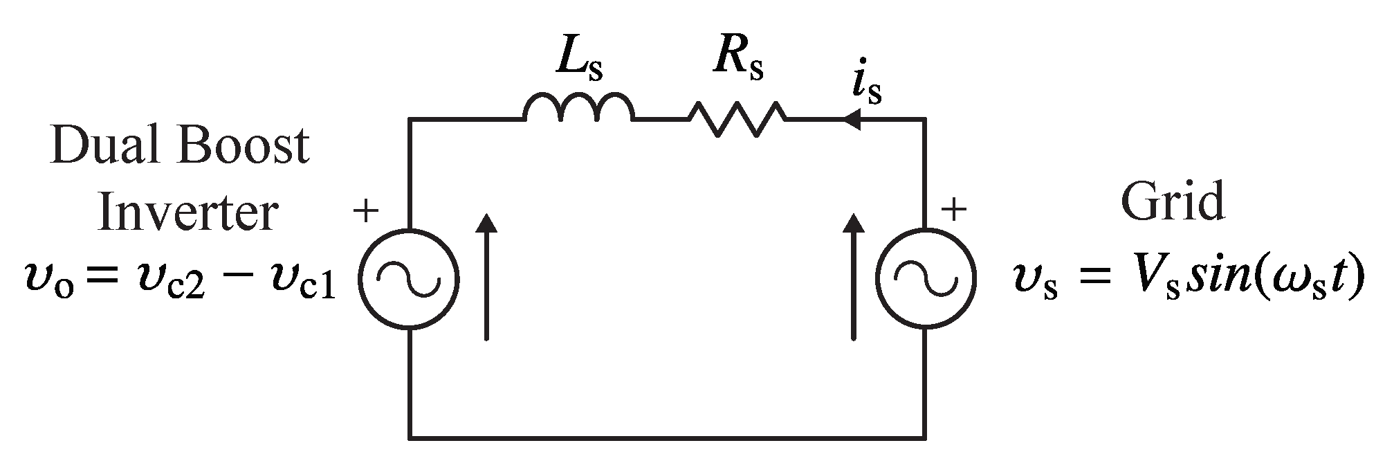
7) shows that the non-linearity of the inverter model is preserved. Moreover, the DBI is integrated to the grid through an inductive filter L s ( R s represents the resistance of the inductive filter and grid), as shown in the equivalent circuit of Figure 3, and the voltage equation can be obtained by
L s d i s ( t ) d t = υ o ( t ) i s ( t ) R s υ s ( t )

3. Control Strategy

The proposed control of the DBI is shown in Figure 4, which consists of cascaded control loops. The fast non-linear inner control loop, based on sliding mode control, regulates the difference of the current in the inductors of DC–DC boost converters, while the linear and slower outer control loop, manages through a PR the current injected to the grid.

3.1. Inner Current Control Loop

To control the output current of the DBI, the sliding mode approach is proposed in the present work for the non-linear inner control loop, due to its inherent properties guaranteeing stability and robustness against variation of parameters with high regulation dynamics, as shown in [21,22]. The analysis here developed has its foundation in the state variables behavior of the dual boost inverter under the presence of a sinusoidal reference introduced in [13]. However, this was solved in [13] for a voltage control loop with a linear load, which cannot be directly extended for a current control for grid-connected applications. This adds a new state variable to the system defined in Equation (8). Thus, it is necessary to adapt the SMC law to fulfill this new control objective. To accomplish this, the analysis is based on the Filippov’s method [23] and its corresponding equivalent control approach.

3.1.1. Sliding Surface Selection

Considering that the output voltage of the inverter is obtained from subtracting the voltage of the capacitors ( υ c 1 and υ c 2 ), and that the capacitor voltage control is related to the inductor current, it is possible to establish that the difference between the current of the inductors controls indirectly the output voltage of the dual boost inverter [3]. Therefore, the sliding surface ( σ ( t ) ) can be defined by
σ ( t ) = k 2 ( t ) + i L 2 ( t ) i L 1 ( t )
where k 2 is the output of external control loop.
Please note that by considering the current derivatives of Equations (4) and (5), the sliding surface can be rewritten as
σ ( t ) = k 2 ( t ) + t 0 t V in L 2 υ c 2 ( t ) L 2 · u ( t ) d t t 0 t V in L 1 υ c 1 ( t ) L 1 · 1 u ( t ) d t

3.1.2. Equivalent Control

In other to guarantee that the sliding mode is maintained on the selected surface, it is necessary to find the equivalent control ( u eq ) through the invariance condition given by
d σ d t σ = 0 u = u eq = 0
Hence, the derivative of the sliding surface evaluated in σ = 0 and u = u eq is
d σ d t = d k 2 ( t ) d t + V in L 2 υ c 2 ( t ) L 2 · u eq ( t ) V in L 1 + υ c 1 ( t ) L 1 · 1 u eq ( t ) = 0
From (12) and due to the symmetry of the inverter ( L = L 1 = L 2 ), the equivalent control is defined as
u eq ( t ) = d k 2 ( t ) d t + υ c 1 ( t ) L L υ c 1 ( t ) + υ c 2 ( t )

3.1.3. Existence Condition

With the expression of equivalent control in Equation (13), the next step is to prove the existence condition, which can be determined by
σ ( x , t ) · d σ ( x , t ) d t < 0
Thus, the derivative of the surface is replaced in Equation (14), expressing the existence condition as
σ d k 2 ( t ) d t + V in L υ c 2 ( t ) L · u ( t ) V in L + υ c 1 ( t ) L · 1 u ( t ) < 0
To establish a relationship between u ( t ) and u eq ( t ) , the expression u eq ( t ) + u eq ( t ) = 0 is added in Equation (15), resulting in
σ d k 2 ( t ) d t + V in L υ c 2 ( t ) L · u ( t ) u eq ( t ) + u eq ( t ) = 0 V in L + υ c 1 ( t ) L · 1 u ( t ) u eq ( t ) + u eq ( t ) = 0 < 0
It is possible to reduce (16) by considering Equation (12), which leads to
σ υ c 1 t + υ c 2 t L · u t + u eq ( t ) < 0
Finally, evaluating (17), and considering that v c 1 > 0 , v c 2 > 0 and L > 0 , it can be determined that if the switching surface is positive, the term ( u ( t ) + u eq ( t ) ) should be negative to accomplish the existence condition, which implies u = u + = 1 . Otherwise, if the switching surface is negative, the term ( u ( t ) + u eq ( t ) ) should be positive and the action control takes the minimum value ( u = u = 0 ), which can be expressed as
σ > 0 and u > u eq u = u + = 1 σ < 0 and u < u eq u = u = 0
The control action defined by Equation (18) leads to the state trajectory to slide on the switching surface and eventually reach the intersection of the switching surface and the equilibrium point converging in a finite time, as demonstrated in [13].

3.2. Outer Current Loop

The main goal of this loop is to regulate the grid current of the DBI. The angle of i s * is obtained from a PLL, which is used to reconstruct a sinusoidal waveform enabling synchronization with the grid [24,25]. The amplitude for the current reference will be considered to be a given value, provided externally to fulfill purposes of the application. Since the current reference is sinusoidal, a proportional resonant controller is used, which is tuned to the grid angular frequency ω s .

3.2.1. Linearization

To design the controller of the outer loop, it is necessary to find the transfer function between the grid current i s and the output of the external control loop k 2 . The equivalent control approach (Equation (13)) is used to introduce the variable k 2 in the averaged switched model of the inverter. Therefore, the equivalent control of u eq ( t ) and its complement ( 1 u eq ( t ) ) are redefined as
u eq ( t ) = υ c 1 ( t ) υ c 1 ( t ) + υ c 2 ( t ) L υ c 1 ( t ) + υ c 2 ( t ) · d k 2 ( t ) d t
1 u eq ( t ) = υ c 2 ( t ) υ c 1 ( t ) + υ c 2 ( t ) + L υ c 1 ( t ) + υ c 2 ( t ) · d k 2 ( t ) d t
The control signals u ( t ) and 1 u ( t ) are substituted by the equivalent control u eq ( t ) and 1 u eq ( t ) in Equations (4)–(7), where it is possible to identify that the derivative of current through L 1 presents the same behavior of the derivative of i L 2 . For this reason, i L 1 was omitted and the state variables of the non-linear model are defined by
x ˙ ( t ) = f x ( t ) + B u ( t ) y ( t ) = C x ( t )
where
f ( x ) = f 1 f 2 f 3 f 4 = x 1 ˙ x 2 ˙ x 3 ˙ x 4 ˙ = d i L 2 ( t ) d t d υ c 1 ( t ) d t d υ c 2 ( t ) d t d i s ( t ) d t y = i s = x 4 u = k 2
Taking into account that σ ( t ) = 0 , the current through inductor L 1 can be obtained as,
i L 1 ( t ) = i L 2 ( t ) k 2 ( t )
Considering (23), υ o = υ c 2 υ c 1 , and that the value of the capacitors are the same C 1 = C 2 = C , the linear model of the system can be expressed as
x ˙ = x 1 ˙ x 2 ˙ x 3 ˙ x 4 ˙ = 0 1 4 L 1 4 L 0 1 2 C 0 0 1 C 1 2 C 0 0 1 C 0 1 L s 1 L s R s L s A · x 1 x 2 x 3 x 4 + 0 1 2 C 0 0 B · u + 1 L 0 0 0 E · p
y = 0 0 0 1 C · x 1 x 2 x 3 x 4
Please note that the same equilibrium point shown in [13] was used in this analysis, which is defined as [ x 10 , x 20 , x 30 , x 40 , k 20 ] = [ 0 , 2 · V in , 2 · V in , 0 , 0 ] .
Considering the equations in Laplace domain, the transfer function can be defined as
G ( s ) = y ( s ) u ( s ) = C · s I A 1 · B
Replacing the matrices and performing some algebraic operations, the relation between the grid current i s and k 2 can be derived as
G ( s ) = y ( s ) u ( s ) = i s ( s ) k 2 ( s ) = 1 2 C L s · 1 s 2 + R s L s s + 2 C L s
Please note that the transfer function is of second order and depends only on the capacitor value, the grid filter, and the grid resistance.

3.2.2. Outer Control Design

The plant G ( s ) is critically stable because it presents a complex conjugate pole pair in the left half-plane close to the imaginary axis. To better illustrate this issue, the frequency response of the plant is shown in Figure 5a, where a significant resonant peak located at 1 kHz can be appreciated. To compensate this peak, to assure a zero steady-state error at 60 Hz (grid frequency) and to regulate the grid current of the inverter, a PR controller is used. The transfer function of the PR controller in the Laplace domain is given by
C PR ( s ) = k p + 2 k i ω c s s 2 + 2 ω c s + ω o 2
where k p is the proportional gain, k i is the resonant gain, ω c is the cut-off frequency, and ω o is the fundamental frequency. Please note that to deal with the sensitivity issue of the ideal PR controller, a bandwidth around the resonant frequency of the controller is added through the cut-off frequency, obtaining a non-ideal PR controller with finite gain [26]. The parameters applied to calculate the PR controller are shown in Table 1.
The closed-loop Bode diagram of the system ( T 1 ) is shown in Figure 5b. Although a finite gain at grid frequency is introduced to obtain a zero-state error in the tracking of the grid current reference, a sufficient degree of the relative stability is not achieved, since the phase margin is equal to zero [27]. Therefore, a phase compensator C ϕ is included to increase the phase margin. The transfer function of this compensator is given by
C ϕ ( s ) = k · s + a s + b
This compensator is composed of a pole and a zero to incorporate phase in the system [28]. As a result, the effect of the cascaded phase compensator is shown in the bode diagram of closed-loop T 2 ( s ) of Figure 5b, where a phase margin of 31.1° is achieved. The parameters of the phase compensator are shown in Table 1.
In addition, to avoid an offset in the grid current of the inverter, due to the fact that in a practical implementation both dc–dc converters will not be exactly the same, an integration term is incorporated in the control scheme, as shown in Figure 4, to force the steady-state error to zero at ω = 0 .

4. Experimental Results

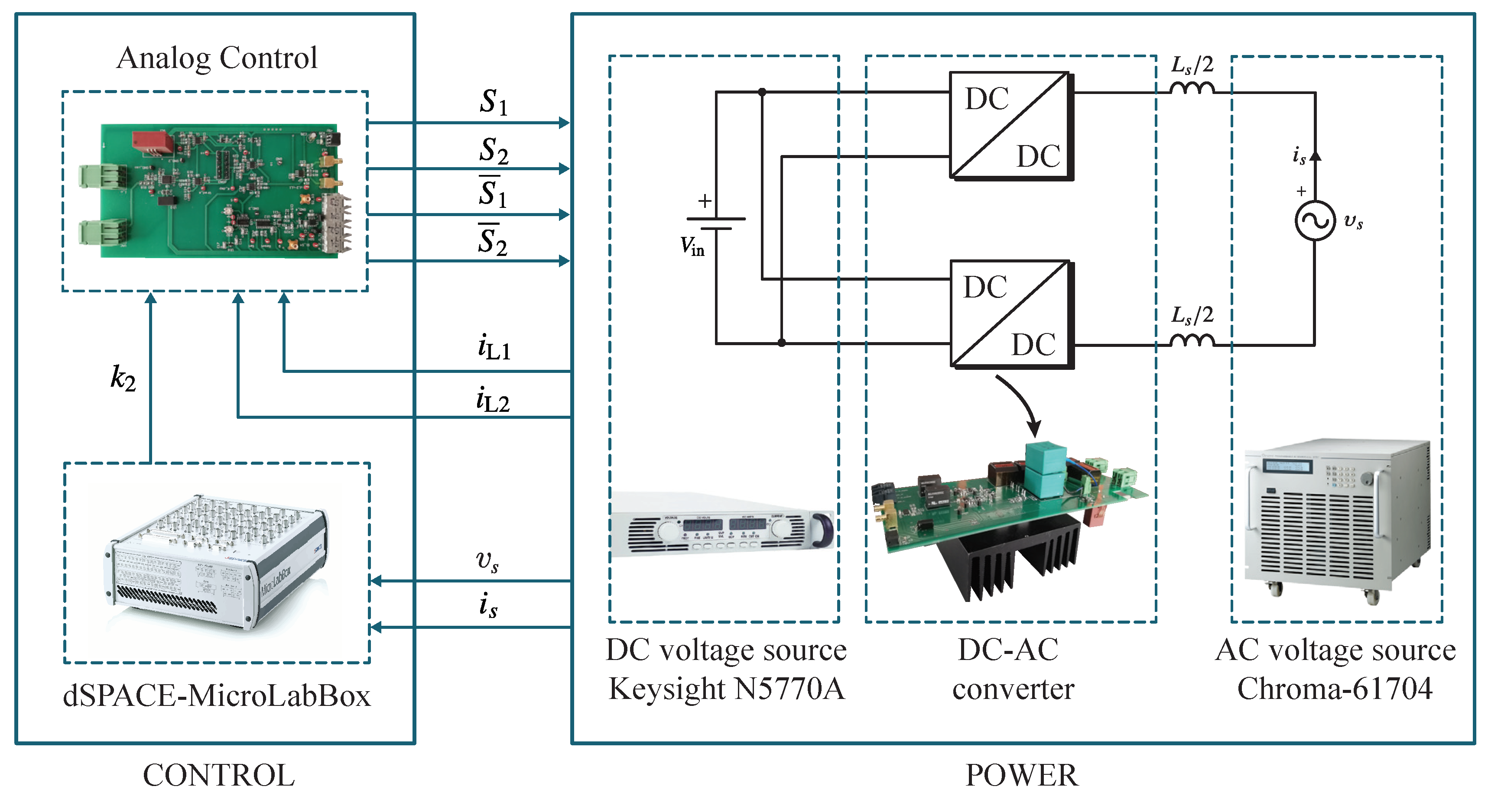
The proposed control for the DBI is validated using the experimental setup shown in Figure 6. The experimental prototype is composed of the power and control parts. In the power part, two dc–dc boost converters have been connected in differential mode, the differential output is connected to the grid through a line filter. The nominal parameters of the setup are summarized in Table 1.
Conventional control systems for power converters are implemented using digital platforms such as DSP and FPGA, due to their fast computational times. On the other hand, sliding mode control is commonly implemented with analog circuits because a hysteresis comparator is used to achieve a finite switching frequency. In this work, a hybrid implementation is proposed taking the advantages of both types of implementation. The phase compensator and PR controller are implemented in a DSpace MicroLabBox platform using Matlab/Simulink, while an analog circuit contains the sliding mode inner control loop, which controls the current in the boost converters. 
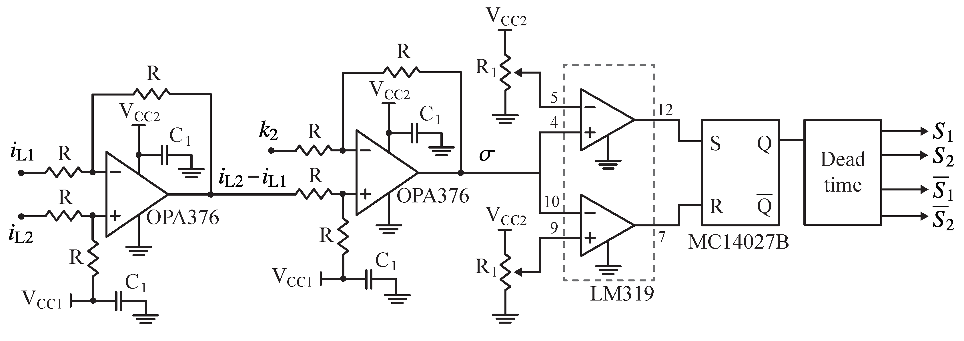
Figure 7 shows the schematic diagram of the analog implementation of the sliding mode controller, where two operational amplifiers are used to generate the switching surface, while the hysteresis is achieved through a comparator LM319 and a J-K Flip-Flop (MC14027B integrated circuit). The hysteresis boundaries given by voltage signals are regulated through variable resistors.
To show the operation of the proposed control, the behavior of the converter is tested when it is connected to the grid. For this purpose, the input has been emulated using a dc voltage source (Keysight N5770A) operating at 70 Vdc, while the grid has been emulated using an AC source (Chroma 61704) operating at 110 Vac,rms/60 Hz . The experimental results are shown in Figure 8.
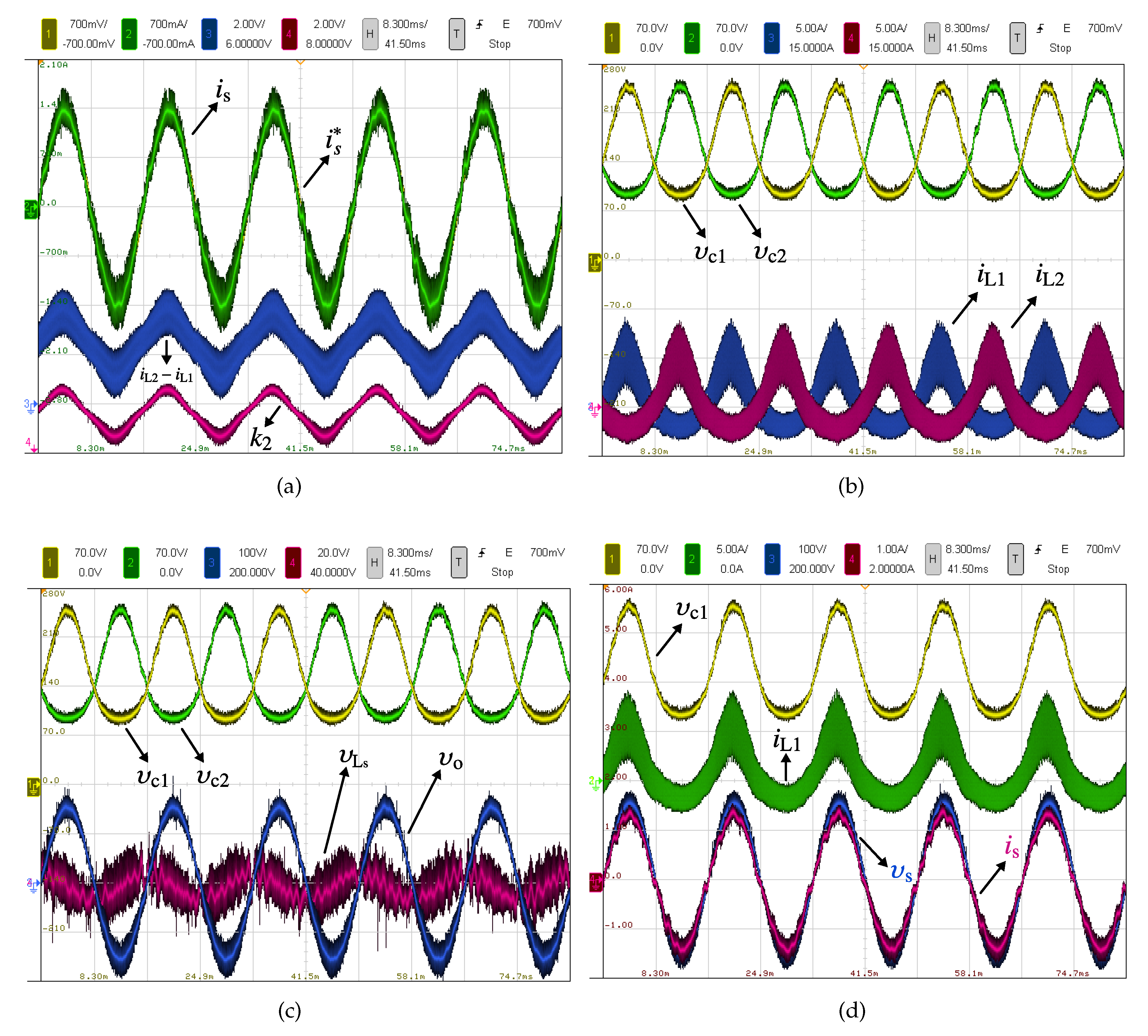
The grid current reference i s * and measured current i s of the DBI are presented in Figure 8a, where it is possible to verify that accurate tracking of the current reference is achieved by the PR controller. The angle of the reference was extracted from the grid voltage υ s , which is shown in Figure 8d. The output of this external control loop k 2 is the reference for the difference between the inductor currents, which can be seen in Figure 8a.
Figure 8b shows the voltage of the capacitors and currents in the inductors, which are balanced despite not being directly controlled. Please note that the magnitudes of the dc and AC components of the output voltages and inductor currents of each dc–dc converter are the same. In the case of the voltages, the dc component of the capacitor voltage is 140 V, which is the double of the input voltage ( V in ). The maximum value of the amplitude of AC component is around 110 V, and the phases of these voltages are shifted by 180°.
From Figure 8c it can be seen that the output voltage of the inverter is sinusoidal, despite the voltage of each capacitor is not purely sinusoidal. Additionally, the condition of proper operation of the inverter ( υ o > υ s ) is fulfilled, because the output voltage of the inverter is around 111 Vac,rms, which is higher than the grid voltage (110 Vac,rms) .
Figure 8d presents the grid current ( i s ) and voltage ( v s ), together with the output voltage and current through the inductance of one of the dc–dc converters. The grid current is very close to a sinusoidal waveform and is always in phase with the grid voltage to ensure the power factor close to unity.
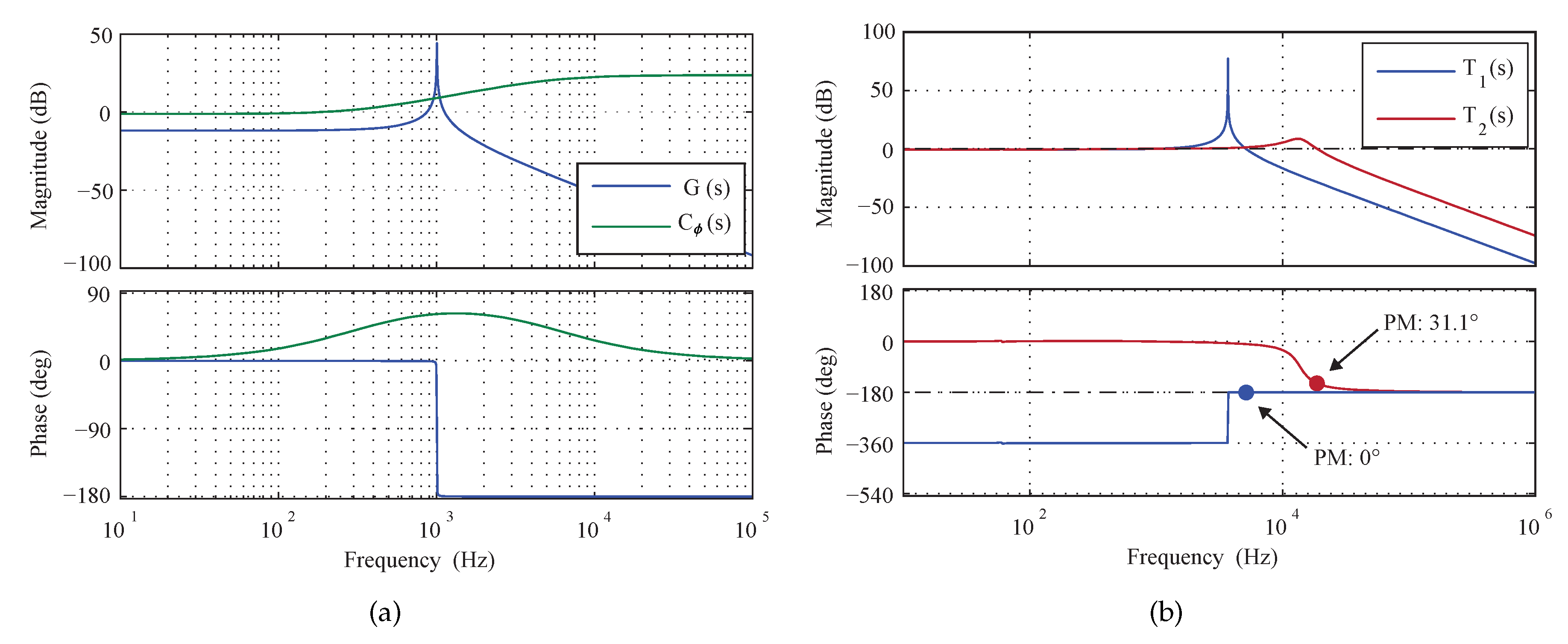
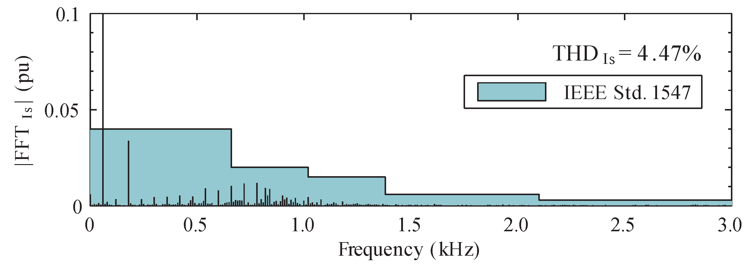
The spectrum and total harmonic distortion (THD) of the grid current in the steady state were obtained to analyze the power quality. These results are presented together with the limits of the IEEE standard 1547 in Figure 9. Note how the harmonics present in the grid current comply with the standard. The total harmonic distortion obtained for the grid current is 4.47%. This is a very good result, considering this is the first iteration of a laboratory prototype (stray inductances and other circuit components have not been optimized), and a simple inductive filter was used for grid connection. The harmonic content could be improved further with higher order filters (such as L C or L C L ), typically used in such applications.
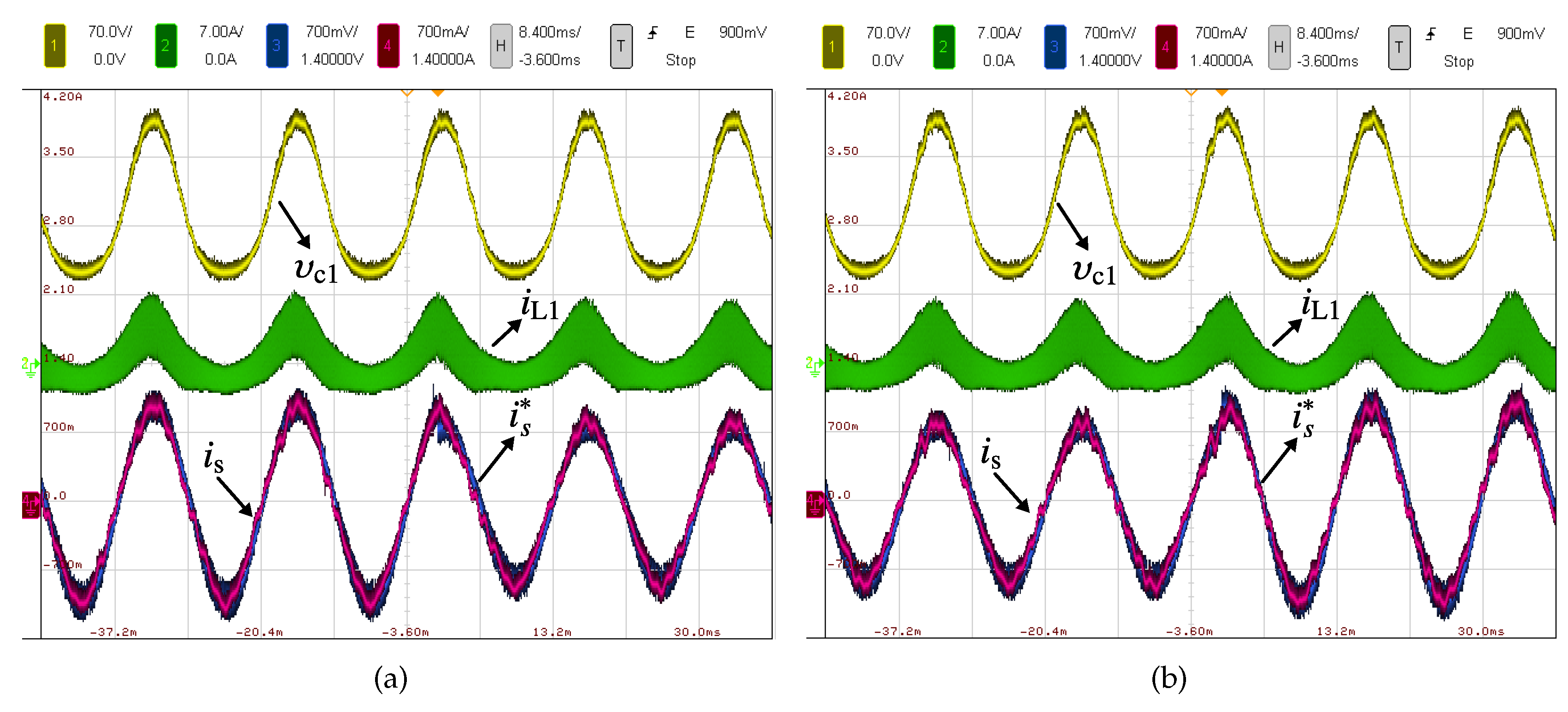
Two tests were performed to evaluate the dynamic performance of the proposed control method. The first test consists of a step-down and a step-up in the output (grid) current reference ( i s * ) to assess the tracking performance. The second test consists on applying a voltage dip in the grid voltage ( v s ) to assess the performance under system perturbations. Figure 10a shows the experimental results associated with the step-down (1.0 to 0.8 A) in the grid current reference, while Figure 10b presents the results obtained for the step-up (0.8 to 1.0 A) in the grid current reference. As illustrated by both figures, a fast dynamic behavior is achieved by the proposed control method, where the tracking of the grid current reference is promptly accomplished. As a result, the grid current variations are reflected in the amplitude of the current through the inductors i L 1 (and i L 2 ); however the voltage of the capacitor υ c 1 (and υ c 2 ) in both cases is kept constant. Both step changes were introduced at the peak value of the current reference, to evaluate the most demanding dynamic scenario for the controller.
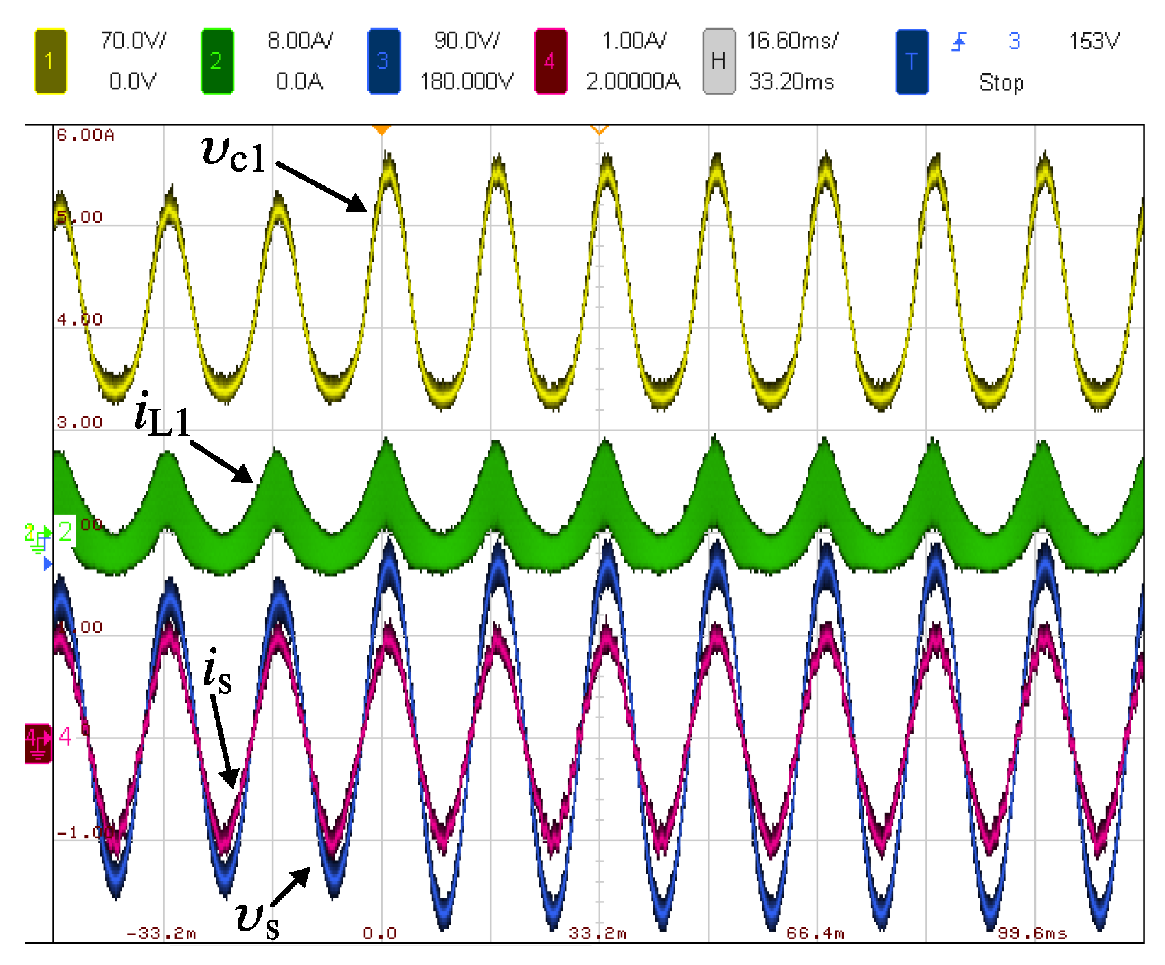
For the second dynamic test, shown in in Figure 11, a voltage dip of 20% was introduced in the grid voltage (only the transition from voltage dip to nominal voltage is shown). The grid voltage amplitude transitions from 88 to 110 Vac,rms. This generates an increase of the AC component in the voltage of both output capacitors ( υ c 1 and υ c 2 ), while the grid current ( i s ) remains controlled without reflecting any change caused by this perturbation, highlighting the robustness of the proposed control method. However, since the inductor current i L 1 (and i L 2 ) depends on the difference between the input voltage v in and the voltage in each output capacitor, a small variation is experienced by i L 1 and i L 2 . Please note that during this test the output (grid) current reference was kept constant.

5. Conclusions

In this paper, a global sliding mode current control scheme for a grid-connected DBI is presented. Two control loops compose the proposed method: the linear PR outer control loop regulates the output current of the inverter (grid current), while the non-linear sliding mode inner control loop regulates the difference between the current of the inductors of the DBI, which allows control of the output voltages of the capacitors indirectly. Hence, fewer control loops are obtained compared to previous control schemes presented for the grid-connected DBI, because the inverter plus grid connection is analyzed globally.
Experimental results show the performance of the proposed control method for a grid-connected DBI. Both reference tracking and power quality show good performance despite using only an inductive filter for grid connection. Hence more sophisticated filters, such as L C or L C L , commonly used in grid-connected applications, could further improve the power quality. In addition, the dc component in the capacitor voltages is double the input voltage, which allows reducing the elevation ratio of the converters, the blocking voltage of the devices, and the capacitor size, compared to traditional methods used for this topology with voltage control loops.
The proposed control method was also tested under dynamic conditions in the current reference and under grid voltage perturbations, achieving good performance in both cases.

Author Contributions

D.L.-C. conceived, designed and performed the experimental evaluations and wrote the original draft; F.F.-B. and S.K. provided practical insight, resources, and supervision and reviewed the manuscript; V.S. was part of the team to design and develop the experimental prototype; N.M. and A.C. reviewed the manuscript and provided practical insight.

Funding

The authors acknowledge the financial support provided by FONDECYT 1191532, AC3E (CONICYT/BASAL/FB0008), SERC Chile (CONICYT/FONDAP/15110019), and CONICYT-PFCHA/Doctorado Nacional/2018-21181781.

Conflicts of Interest

The authors declare no conflict of interest.

References

  1. Kouro, S.; Leon, J.I.; Vinnikov, D.; Franquelo, L.G. Grid-Connected Photovoltaic Systems: An Overview of Recent Research and Emerging PV Converter Technology. IEEE Ind. Electron. Mag. 2015, 9, 47–61. [Google Scholar] [CrossRef]
  2. Caceres, R.; Barbi, I. A boost DC-AC converter: Operation, analysis, control and experimentation. In Proceedings of the 21st Annual Conference on IEEE Industrial Electronics (IECON ’95), Orlando, FL, USA, 6–10 November 1995; Volume 1, pp. 546–551. [Google Scholar] [CrossRef]
  3. Cortes, D.; Vazquez, N.; Alvarez-Gallegos, J. Dynamical Sliding-Mode Control of the Boost Inverter. IEEE Trans. Ind. Electron. 2009, 56, 3467–3476. [Google Scholar] [CrossRef]
  4. Jang, M.; Agelidis, V.G. A Minimum Power-Processing-Stage Fuel-Cell Energy System Based on a Boost-Inverter with a Bidirectional Backup Battery Storage. IEEE Trans. Power Electron. 2011, 26, 1568–1577. [Google Scholar] [CrossRef]
  5. Sanchis, P.; Ursaea, A.; Gubia, E.; Marroyo, L. Boost DC-AC inverter: A new control strategy. IEEE Trans. Power Electron. 2005, 20, 343–353. [Google Scholar] [CrossRef]
  6. Zhu, G.; Tan, S.; Chen, Y.; Tse, C.K. Mitigation of Low-Frequency Current Ripple in Fuel-Cell Inverter Systems through Waveform Control. IEEE Trans. Power Electron. 2013, 28, 779–792. [Google Scholar] [CrossRef]
  7. Jang, M.; Ciobotaru, M.; Agelidis, V.G. A Single-Phase Grid-Connected Fuel Cell System Based on a Boost-Inverter. IEEE Trans. Power Electron. 2013, 28, 279–288. [Google Scholar] [CrossRef]
  8. Abeywardana, D.B.W.; Hredzak, B.; Agelidis, V.G. A Rule-Based Controller to Mitigate DC-Side Second-Order Harmonic Current in a Single-Phase Boost Inverter. IEEE Trans. Power Electron. 2016, 31, 1665–1679. [Google Scholar] [CrossRef]
  9. Caceres, R.O.; Barbi, I. A boost DC-AC converter: Analysis, design, and experimentation. IEEE Trans. Power Electron. 1999, 14, 134–141. [Google Scholar] [CrossRef]
  10. Jha, K.; Mishra, S.; Joshi, A. High-Quality Sine Wave Generation Using a Differential Boost Inverter at Higher Operating Frequency. IEEE Trans. Ind. Appl. 2015, 51, 373–384. [Google Scholar] [CrossRef]
  11. Renaudineau, H.; Lopez, D.; Flores-Bahamonde, F.; Kouro, S. Flatness-based control of a boost inverter for PV microinverter application. In Proceedings of the 2017 IEEE 8th International Symposium on Power Electronics for Distributed Generation Systems (PEDG), Florianopolis, Brazil, 17–20 April 2017; pp. 1–6. [Google Scholar] [CrossRef]
  12. Lopez, D.; Flores-Bahamonde, F.; Kouro, S.; Perez, M.A.; Llor, A.; Martínez-Salamero, L. Predictive control of a single-stage boost DC-AC photovoltaic microinverter. In Proceedings of the IECON 2016, 42nd Annual Conference of the IEEE Industrial Electronics Society, Florence, Italy, 23–26 October 2016; pp. 6746–6751. [Google Scholar] [CrossRef]
  13. Flores-Bahamonde, F.; Valderrama-Blavi, H.; Bosque-Moncusi, J.M.; García, G.; Martínez-Salamero, L. Using the sliding-mode control approach for analysis and design of the boost inverter. IET Power Electron. 2016, 9, 1625–1634. [Google Scholar] [CrossRef]
  14. Wang, Y.; Yu, D.; Kim, Y. Robust Time-Delay Control for the DC–DC Boost Converter. IEEE Trans. Ind. Electron. 2014, 61, 4829–4837. [Google Scholar] [CrossRef]
  15. Pandey, S.K.; Patil, S.L.; Phadke, S.B. Comment on “PWM-Based Adaptive Sliding-Mode Control for Boost DC–DC Converters” [Aug 13 3291-3294]. IEEE Trans. Ind. Electron. 2018, 65, 5078–5080. [Google Scholar] [CrossRef]
  16. Ma, R.; Wu, Y.; Breaz, E.; Huangfu, Y.; Briois, P.; Gao, F. High-order Sliding Mode Control of DC-DC Converter for PEM Fuel Cell Applications. In Proceedings of the 2018 IEEE Industry Applications Society Annual Meeting (IAS), Portland, OR, USA, 23–27 September 2018; pp. 1–7. [Google Scholar]
  17. Liu, Y.; Huang, M.; Sun, J.; Zha, X. Active power decoupling method for isolated micro-inverters. In Proceedings of the 2014 International Power Electronics and Application Conference and Exposition, Shanghai, China, 5–8 November 2014; pp. 1222–1225. [Google Scholar] [CrossRef]
  18. Kjær, S.B.; Blaabjerg, F. A novel single-stage inverter for the AC-module with reduced low-frequency ripple penetration. In Proceedings of the Epe’2003, Toulouse, France, 2–4 September 2003. [Google Scholar]
  19. Mazumder, S.K.; Mehrnami, S. A low-device-count single-stage direct-power-conversion solar microinverter for microgrid. In Proceedings of the 2012 3rd IEEE International Symposium on Power Electronics for Distributed Generation Systems (PEDG), Aalborg, Denmark, 25–28 June 2012; pp. 725–730. [Google Scholar] [CrossRef]
  20. Mehrnami, S.; Mazumder, S.K. Discontinuous Modulation Scheme for a Differential-Mode Ćuk Inverter. IEEE Trans. Power Electron. 2015, 30, 1242–1254. [Google Scholar] [CrossRef]
  21. Skvarenina, T.L. The Power Electronics Handbook; CRC Press: Boca Raton, FL, USA, 2002. [Google Scholar]
  22. Vecchio, C. Sliding Mode Control: Theoretical Developments and Applications to Uncertain Mechanical Systems. Ph.D. Thesis, The University of Pavia, Pavia, Italy, 2008. [Google Scholar]
  23. Arscott, F.; Filippov, A. Differential Equations with Discontinuous Righthand Sides: Control Systems; Mathematics and Its Applications; Springer: Dordrecht, The Netherlands, 1988. [Google Scholar]
  24. Teodorescu, R.; Liserre, M.; Rodriguez, P. Grid Converters for Photovoltaic and Wind Power Systems; John Wiley & Sons: Hoboken, NJ, USA, 2011; Volume 29. [Google Scholar]
  25. Rodríguez, P.; Luna, A.; Muñoz-Aguilar, R.S.; Etxeberria-Otadui, I.; Teodorescu, R.; Blaabjerg, F. A Stationary Reference Frame Grid Synchronization System for Three-Phase Grid-Connected Power Converters Under Adverse Grid Conditions. IEEE Trans. Power Electron. 2012, 27, 99–112. [Google Scholar] [CrossRef]
  26. Teodorescu, R.; Blaabjerg, F.; Liserre, M.; Loh, P.C. Proportional-resonant controllers and filters for grid-connected voltage-source converters. IEE Proc. Electr. Power Appl. 2006, 153, 750–762. [Google Scholar] [CrossRef] [Green Version]
  27. Kazimierczuk, M. Pulse-Width Modulated DC-DC Power Converters; Wiley: Hoboken, NJ, USA, 2008. [Google Scholar]
  28. Corradini, L.; Maksimovic, D.; Mattavelli, P.; Zane, R. Digital Control of High-Frequency Switched-Mode Power Converters; IEEE Press Series on Power Engineering; Wiley: Hoboken, NJ, USA, 2015. [Google Scholar]
Figure 1. The generic concept of a single-stage step-up differential mode inverter.
Energies 12 04241 g001
Figure 2. Dual boost inverter topology.
Energies 12 04241 g002
Figure 3. Equivalent model of the DBI with grid connection.
Energies 12 04241 g003
Figure 4. The cascaded control scheme of the grid-connected DBI, with external PR controller and internal sliding mode controller.
Energies 12 04241 g004
Figure 5. Bode diagrams: (a) plant and phase compensator, (b) closed-loop without and with the phase compensator.
Energies 12 04241 g005
Figure 6. Experimental diagram of dual boost inverter.
Energies 12 04241 g006
Figure 7. Analog circuit for control stage, where R = 20 kΩ, R1 = 10 kΩ, V C C 1 = 2.5 V, V C C 2 = 5 V, and C 1 = 0.1 µF.
Energies 12 04241 g007
Figure 8. Experimental results with grid connection and input voltage of 70 V: (a) reference and measurement of grid current, difference of the inductor currents and output of outer control loop ( k 2 ), (b) voltage of the capacitors ( υ c 1 , υ c 2 ) and current through the inductors ( i L 1 , i L 2 ), (c) voltage of the capacitors ( υ c 1 , υ c 2 ), voltage of the line filter, output voltage ( υ o ) and (d) υ c 1 , i L 1 , grid voltage and current.
Energies 12 04241 g008
Figure 9. Grid current spectrum with 70 V of input voltage.
Energies 12 04241 g009
Figure 10. Experimental results under variations in the output current reference (voltage of the capacitor C 1 ( υ c 1 ), current through the inductor L 1 ( i L 1 ), reference ( i s * ) and measurement ( i s ) of grid current): (a) Step-down in the output current reference, and (b) Step-up in the output current reference.
Energies 12 04241 g010
Figure 11. Experimental dynamic performance under grid perturbation (from 20% voltage dip to nominal voltage): voltage of the capacitor C 1 ( υ c 1 ), current through the inductor L 1 ( i L 1 ), measurement of grid current ( i s ), and grid voltage ( υ s ).
Energies 12 04241 g011
Table 1. Main parameters of the experimental setup.
SymbolParameterExperimental Value
Grid Parameters
υ s Grid voltage110 [ V rms ]
f s Grid frequency60 [Hz]
L s Grid filter inductance10 [mH]
Converter Parameters
V in Input voltage70 [V]
L 1 , L 2 Inverter inductors55 [µH]
C 1 , C 2 Inverter capacitors5 [µF]
Control Parameters
kGain of C ϕ 1
k p Proportional gain of PR50
k i Resonant gain of PR700
ω c Cut-off frequency of PR5 [rad/s]
aZero of phase compensator2000
bPole of phase compensator35,000

